EP2429005A2 - Method for manufacturing a mono-crystalline silicon solar cell and etching method thereof - Google Patents
Method for manufacturing a mono-crystalline silicon solar cell and etching method thereof Download PDFInfo
- Publication number
- EP2429005A2 EP2429005A2 EP11180978A EP11180978A EP2429005A2 EP 2429005 A2 EP2429005 A2 EP 2429005A2 EP 11180978 A EP11180978 A EP 11180978A EP 11180978 A EP11180978 A EP 11180978A EP 2429005 A2 EP2429005 A2 EP 2429005A2
- Authority
- EP
- European Patent Office
- Prior art keywords
- compound
- crystalline silicon
- mono
- ions
- alkaline solution
- Prior art date
- Legal status (The legal status is an assumption and is not a legal conclusion. Google has not performed a legal analysis and makes no representation as to the accuracy of the status listed.)
- Withdrawn
Links
- 229910021421 monocrystalline silicon Inorganic materials 0.000 title claims abstract description 65
- 238000005530 etching Methods 0.000 title claims abstract description 60
- 238000000034 method Methods 0.000 title claims abstract description 40
- 238000004519 manufacturing process Methods 0.000 title claims abstract description 27
- SQGYOTSLMSWVJD-UHFFFAOYSA-N silver(1+) nitrate Chemical compound [Ag+].[O-]N(=O)=O SQGYOTSLMSWVJD-UHFFFAOYSA-N 0.000 claims description 87
- -1 alcohol compound Chemical class 0.000 claims description 64
- 239000012670 alkaline solution Substances 0.000 claims description 61
- 150000001875 compounds Chemical class 0.000 claims description 57
- KWYUFKZDYYNOTN-UHFFFAOYSA-M Potassium hydroxide Chemical compound [OH-].[K+] KWYUFKZDYYNOTN-UHFFFAOYSA-M 0.000 claims description 48
- 150000002500 ions Chemical class 0.000 claims description 31
- 239000000654 additive Substances 0.000 claims description 26
- 230000000996 additive effect Effects 0.000 claims description 26
- 229910052709 silver Inorganic materials 0.000 claims description 26
- 239000004332 silver Substances 0.000 claims description 26
- KFZMGEQAYNKOFK-UHFFFAOYSA-N Isopropanol Chemical compound CC(C)O KFZMGEQAYNKOFK-UHFFFAOYSA-N 0.000 claims description 24
- HEMHJVSKTPXQMS-UHFFFAOYSA-M Sodium hydroxide Chemical compound [OH-].[Na+] HEMHJVSKTPXQMS-UHFFFAOYSA-M 0.000 claims description 24
- 229940100890 silver compound Drugs 0.000 claims description 19
- 150000003379 silver compounds Chemical class 0.000 claims description 19
- 229910000510 noble metal Inorganic materials 0.000 claims description 17
- 229910000367 silver sulfate Inorganic materials 0.000 claims description 11
- 239000010931 gold Substances 0.000 claims description 10
- KDLHZDBZIXYQEI-UHFFFAOYSA-N palladium Substances [Pd] KDLHZDBZIXYQEI-UHFFFAOYSA-N 0.000 claims description 10
- BASFCYQUMIYNBI-UHFFFAOYSA-N platinum Substances [Pt] BASFCYQUMIYNBI-UHFFFAOYSA-N 0.000 claims description 10
- 229910052737 gold Inorganic materials 0.000 claims description 8
- 229910052763 palladium Inorganic materials 0.000 claims description 8
- 229910052697 platinum Inorganic materials 0.000 claims description 8
- 239000012535 impurity Substances 0.000 claims description 7
- LFQSCWFLJHTTHZ-UHFFFAOYSA-N Ethanol Chemical compound CCO LFQSCWFLJHTTHZ-UHFFFAOYSA-N 0.000 claims description 5
- 230000003667 anti-reflective effect Effects 0.000 claims description 5
- 229910021419 crystalline silicon Inorganic materials 0.000 claims description 5
- 239000005360 phosphosilicate glass Substances 0.000 claims description 5
- BDERNNFJNOPAEC-UHFFFAOYSA-N propan-1-ol Chemical compound CCCO BDERNNFJNOPAEC-UHFFFAOYSA-N 0.000 claims description 2
- GGCZERPQGJTIQP-UHFFFAOYSA-N sodium;9,10-dioxoanthracene-2-sulfonic acid Chemical compound [Na+].C1=CC=C2C(=O)C3=CC(S(=O)(=O)O)=CC=C3C(=O)C2=C1 GGCZERPQGJTIQP-UHFFFAOYSA-N 0.000 claims 2
- 150000007522 mineralic acids Chemical class 0.000 claims 1
- 150000007524 organic acids Chemical class 0.000 claims 1
- XUIMIQQOPSSXEZ-UHFFFAOYSA-N Silicon Chemical compound [Si] XUIMIQQOPSSXEZ-UHFFFAOYSA-N 0.000 abstract description 10
- 229910052710 silicon Inorganic materials 0.000 abstract description 10
- 239000010703 silicon Substances 0.000 abstract description 10
- BQCADISMDOOEFD-UHFFFAOYSA-N Silver Chemical compound [Ag] BQCADISMDOOEFD-UHFFFAOYSA-N 0.000 abstract description 3
- 229910021645 metal ion Inorganic materials 0.000 abstract 2
- 230000003197 catalytic effect Effects 0.000 abstract 1
- 235000012431 wafers Nutrition 0.000 description 28
- 238000001039 wet etching Methods 0.000 description 14
- XLYOFNOQVPJJNP-UHFFFAOYSA-N water Substances O XLYOFNOQVPJJNP-UHFFFAOYSA-N 0.000 description 8
- 230000015572 biosynthetic process Effects 0.000 description 6
- 229910000108 silver(I,III) oxide Inorganic materials 0.000 description 6
- 238000009792 diffusion process Methods 0.000 description 5
- 238000002955 isolation Methods 0.000 description 5
- 239000002244 precipitate Substances 0.000 description 5
- 239000000243 solution Substances 0.000 description 5
- 230000003071 parasitic effect Effects 0.000 description 4
- OAICVXFJPJFONN-UHFFFAOYSA-N Phosphorus Chemical compound [P] OAICVXFJPJFONN-UHFFFAOYSA-N 0.000 description 3
- 230000008901 benefit Effects 0.000 description 3
- 238000000608 laser ablation Methods 0.000 description 3
- 239000000203 mixture Substances 0.000 description 3
- 239000011574 phosphorus Substances 0.000 description 3
- 229910052698 phosphorus Inorganic materials 0.000 description 3
- KRHYYFGTRYWZRS-UHFFFAOYSA-N Fluorane Chemical compound F KRHYYFGTRYWZRS-UHFFFAOYSA-N 0.000 description 2
- GRYLNZFGIOXLOG-UHFFFAOYSA-N Nitric acid Chemical compound O[N+]([O-])=O GRYLNZFGIOXLOG-UHFFFAOYSA-N 0.000 description 2
- 239000002253 acid Substances 0.000 description 2
- 239000003929 acidic solution Substances 0.000 description 2
- 239000006227 byproduct Substances 0.000 description 2
- 230000007423 decrease Effects 0.000 description 2
- 238000010586 diagram Methods 0.000 description 2
- 238000012986 modification Methods 0.000 description 2
- 230000004048 modification Effects 0.000 description 2
- 229910017604 nitric acid Inorganic materials 0.000 description 2
- XHXFXVLFKHQFAL-UHFFFAOYSA-N phosphoryl trichloride Chemical compound ClP(Cl)(Cl)=O XHXFXVLFKHQFAL-UHFFFAOYSA-N 0.000 description 2
- 229910021420 polycrystalline silicon Inorganic materials 0.000 description 2
- 229910017988 AgVO3 Inorganic materials 0.000 description 1
- 229910019213 POCl3 Inorganic materials 0.000 description 1
- 229910021607 Silver chloride Inorganic materials 0.000 description 1
- 230000002378 acidificating effect Effects 0.000 description 1
- 150000001298 alcohols Chemical class 0.000 description 1
- 239000007864 aqueous solution Substances 0.000 description 1
- WIKQEUJFZPCFNJ-UHFFFAOYSA-N carbonic acid;silver Chemical compound [Ag].[Ag].OC(O)=O WIKQEUJFZPCFNJ-UHFFFAOYSA-N 0.000 description 1
- 239000011248 coating agent Substances 0.000 description 1
- 238000000576 coating method Methods 0.000 description 1
- 230000008878 coupling Effects 0.000 description 1
- 238000010168 coupling process Methods 0.000 description 1
- 238000005859 coupling reaction Methods 0.000 description 1
- 239000007788 liquid Substances 0.000 description 1
- 239000000463 material Substances 0.000 description 1
- 238000007639 printing Methods 0.000 description 1
- 230000009467 reduction Effects 0.000 description 1
- 238000002310 reflectometry Methods 0.000 description 1
- ADZWSOLPGZMUMY-UHFFFAOYSA-M silver bromide Chemical compound [Ag]Br ADZWSOLPGZMUMY-UHFFFAOYSA-M 0.000 description 1
- LKZMBDSASOBTPN-UHFFFAOYSA-L silver carbonate Substances [Ag].[O-]C([O-])=O LKZMBDSASOBTPN-UHFFFAOYSA-L 0.000 description 1
- LFAGQMCIGQNPJG-UHFFFAOYSA-N silver cyanide Chemical compound [Ag+].N#[C-] LFAGQMCIGQNPJG-UHFFFAOYSA-N 0.000 description 1
- HKZLPVFGJNLROG-UHFFFAOYSA-M silver monochloride Chemical compound [Cl-].[Ag+] HKZLPVFGJNLROG-UHFFFAOYSA-M 0.000 description 1
- KQTXIZHBFFWWFW-UHFFFAOYSA-L silver(I) carbonate Inorganic materials [Ag]OC(=O)O[Ag] KQTXIZHBFFWWFW-UHFFFAOYSA-L 0.000 description 1
- 238000005507 spraying Methods 0.000 description 1
- 239000000126 substance Substances 0.000 description 1
- 239000010409 thin film Substances 0.000 description 1
Images


Classifications
-
- H—ELECTRICITY
- H01—ELECTRIC ELEMENTS
- H01L—SEMICONDUCTOR DEVICES NOT COVERED BY CLASS H10
- H01L31/00—Semiconductor devices sensitive to infrared radiation, light, electromagnetic radiation of shorter wavelength or corpuscular radiation and specially adapted either for the conversion of the energy of such radiation into electrical energy or for the control of electrical energy by such radiation; Processes or apparatus specially adapted for the manufacture or treatment thereof or of parts thereof; Details thereof
- H01L31/02—Details
- H01L31/0236—Special surface textures
- H01L31/02363—Special surface textures of the semiconductor body itself, e.g. textured active layers
-
- H—ELECTRICITY
- H01—ELECTRIC ELEMENTS
- H01L—SEMICONDUCTOR DEVICES NOT COVERED BY CLASS H10
- H01L31/00—Semiconductor devices sensitive to infrared radiation, light, electromagnetic radiation of shorter wavelength or corpuscular radiation and specially adapted either for the conversion of the energy of such radiation into electrical energy or for the control of electrical energy by such radiation; Processes or apparatus specially adapted for the manufacture or treatment thereof or of parts thereof; Details thereof
- H01L31/18—Processes or apparatus specially adapted for the manufacture or treatment of these devices or of parts thereof
- H01L31/1804—Processes or apparatus specially adapted for the manufacture or treatment of these devices or of parts thereof comprising only elements of Group IV of the Periodic System
-
- Y—GENERAL TAGGING OF NEW TECHNOLOGICAL DEVELOPMENTS; GENERAL TAGGING OF CROSS-SECTIONAL TECHNOLOGIES SPANNING OVER SEVERAL SECTIONS OF THE IPC; TECHNICAL SUBJECTS COVERED BY FORMER USPC CROSS-REFERENCE ART COLLECTIONS [XRACs] AND DIGESTS
- Y02—TECHNOLOGIES OR APPLICATIONS FOR MITIGATION OR ADAPTATION AGAINST CLIMATE CHANGE
- Y02E—REDUCTION OF GREENHOUSE GAS [GHG] EMISSIONS, RELATED TO ENERGY GENERATION, TRANSMISSION OR DISTRIBUTION
- Y02E10/00—Energy generation through renewable energy sources
- Y02E10/50—Photovoltaic [PV] energy
- Y02E10/547—Monocrystalline silicon PV cells
-
- Y—GENERAL TAGGING OF NEW TECHNOLOGICAL DEVELOPMENTS; GENERAL TAGGING OF CROSS-SECTIONAL TECHNOLOGIES SPANNING OVER SEVERAL SECTIONS OF THE IPC; TECHNICAL SUBJECTS COVERED BY FORMER USPC CROSS-REFERENCE ART COLLECTIONS [XRACs] AND DIGESTS
- Y02—TECHNOLOGIES OR APPLICATIONS FOR MITIGATION OR ADAPTATION AGAINST CLIMATE CHANGE
- Y02P—CLIMATE CHANGE MITIGATION TECHNOLOGIES IN THE PRODUCTION OR PROCESSING OF GOODS
- Y02P70/00—Climate change mitigation technologies in the production process for final industrial or consumer products
- Y02P70/50—Manufacturing or production processes characterised by the final manufactured product
Abstract
Description
- The present invention relates to a novel method for manufacturing a mono-crystalline or a quasi-mono-crystalline silicon solar cell and a wet etching method thereof. It relates in particular to a method for manufacturing a mono-crystalline or a quasi-mono-crystalline silicon solar cell and a wet etching method thereof which can increase the production rate.
- Solar cells are the devices that convert light energy into electrical energy, and they may be categorized as the thin-film solar cells and the crystalline solar cells. Major materials presently used for crystalline solar cells in the market include silicon, and the crystalline silicon solar cells can be further sorted into mono-crystalline silicon solar cells, quasi-mono-crystalline silicon solar cells and multi-crystalline silicon solar cells. A quasi-mono-crystalline silicon wafer refers to a silicon wafer containing a mono-crystalline phase and many multi-crystalline phases, with the majority of the wafer being in a mono-crystalline phase. For simplicity in the following paragraphs, the word "mono-crystalline" may refer to both mono-crystalline and quasi-mono-crystalline as well.
- A manufacturing process of p-type crystalline silicon solar cells includes a surface texturization (texture etching) step, a phosphorus diffusion step, a step for removing a surface oxide layer, a step for forming an anti-reflective layer, a step for forming electrodes, a laser-ablation edge isolation step. Another manufacturing process thereof includes a surface texturization (texture etching) step, a phosphorus diffusion step, a wet etching edge isolation step, a step for removing a surface oxide layer, a step for forming an anti-reflective layer, a step for forming electrodes.
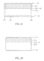
- In the surface texturization step, a surface of a silicon wafer is wet etched by using acidic or alkaline solution. The acidic solution suitable for etching multi-crystalline silicon solar cells typically contains a mixture of hydrofluoric acid and nitric acid, and the alkaline solution suitable for etching mono-crystalline silicon solar cells typically contains a mixture of sodium hydroxide or potassium hydroxide, and at least a kind of alcohol. However, for the mono-crystalline silicon wafers, the wet etching time is usually 20 minutes to 30 minutes for the surface texturization step according to prior art alkaline etching techniques. The silicon etching rate in the alkaline solution can be further increased to improve production throughput.
- In an embodiment, an object of the invention is to provide a method for manufacturing a mono-crystalline silicon solar cell and a wet etching method thereof which increase the production rate of mono-crystalline silicon solar cells. In another embodiment, another object of the invention is to provide a method for manufacturing a mono-crystalline silicon solar cell and a wet etching method thereof which increase the silicon etching rate of the alkaline etching solution.
- According to an embodiment of the invention, a wet etching method applied in a method for manufacturing a mono-crystalline silicon solar cell is provided. The wet etching method comprises a step of etching at least a surface of a mono-crystalline silicon wafer by using an alkaline solution. The alkaline solution contains an alkaline compound containing at least one compound selected from a group consisting of sodium hydroxide and potassium hydroxide, an alcohol compound, and a compound for releasing in the alkaline solution noble metal ions containing at least one ion selected from a group consisting of gold ions, silver ions, platinum ions, and palladium ions.
- According to an embodiment of the invention, a method for manufacturing a mono-crystalline silicon solar cell is provided. The method comprises: etching at least a surface of a first-type mono-crystalline silicon wafer by using an alkaline solution; doping second-type impurities into the first-type mono-crystalline silicon wafer, so as to form a first-type area, a second-type area, and a junction between the first-type area and the second-type area; processing the edges of the first-type mono-crystalline silicon wafer so that there is substantially no short circuit between the edges of the first-type area and the second-type area; etching the surfaces of the mono-crystalline silicon wafer to remove a phosphosilicate glass (PSG) structure on the surfaces; forming an anti-reflective layer on the first-type mono-crystalline silicon wafer; and forming an electrode structure on the first-type mono-crystalline silicon wafer so that the first-type area and the second-type area form a current loop via an external electrical load. The alkaline solution contains an alkaline compound containing at least one compound selected from a group consisting sodium hydroxide and potassium hydroxide, an alcohol compound, and a compound for releasing in the alkaline solution noble metal ions containing at least one ion selected from a group consisting of gold ions, silver ions, platinum ions, and palladium ions.
- In an embodiment of the invention, the noble metal ions may be gold ions, silver ions, platinum ions, palladium ions or the combination thereof. When the noble metal ions is silver ions, the compound for releasing silver ions in the alkaline solution may contain at least one compound selected from a group consisting of AgClO4 and AgNO3. In one embodiment, the compound for releasing silver ions in the alkaline solution may contain at least one compound selected from a group consisting of AgClO3, AgC2H3O2, AgMnO4 and Ag2SO4.
- In an embodiment, the alkaline compound is the potassium hydroxide, and the additive amount of the potassium hydroxide is approximately 1% to 4% by weight. The alcohol compound is an isopropanol (Isopropyl alcohol, abbreviated as IPA), and the additive amount of the isopropanol is approximately 2% to 6% by volume. When the compound for releasing silver ions in the alkaline solution contains at least one compound selected from a group consisting of AgClO4 and AgNO3, the additive amount of the silver compounds is approximately 1 ppm to 100 ppm by weight. When the compound for releasing silver ions in the alkaline solution contains at least one compound selected from a group consisting of AgClO3, AgC2H302, AgMnO4 and Ag2SO4, the additive amount of the silver compounds is approximately 30 ppm to 5000 ppm by weight.
- According to an embodiment of the present invention, since the alkaline solution contains the ions of the above-mentioned four predetermined noble metals, which catalyze the silicon etching by the alkaline compound, and the etching rate in the etching step is effectively increased. As a result, it takes less time to manufacture a mono-crystalline silicon solar cell, and then the productivity of mono-crystalline silicon solar cells is increased.
- Other objectives, features and advantages of the present invention will be further understood from the further technological features disclosed by the embodiments of the present invention wherein there are shown and described preferred embodiments of this invention, simply by way of illustration of modes best suited to carry out the invention.
- The structure and the technical means adopted by the present invention to achieve the above and other objects can be best understood by referring to the following detailed description of the preferred embodiments and the accompanying drawings, wherein:
-
FIGS. 1A~1G respectively show a schematic cross-section diagram of each step of a method for manufacturing a mono-crystalline silicon solar cell according to an embodiment of the present invention. -
FIGS. 2A~2B show a flowchart of a method for manufacturing a mono-crystalline silicon solar cell according to an embodiment of the present invention. - In the following detailed description of the preferred embodiments, reference is made to the accompanying drawings which form a part hereof, and in which is shown by way of illustrating specific embodiments in which the invention may be practiced. In this regard, directional terminology is used with reference to the orientation of the Figure(s) being described. The components of the present invention can be positioned in a number of different orientations. As such, the directional terminology is used for purposes of illustration and is in no way limiting the scope of the present invention. On the other hand, the drawings are only schematic and the sizes of components may be exaggerated for clarity. It is to be understood that other embodiments may be employed and structural changes may be made without departing from the scope of the present invention. Also, it is to be understood that the phraseology and terminology used herein are for the purpose of description and should not be regarded as limiting. The use of "including," "comprising," or "having" and variations thereof herein is meant to encompass the items listed thereafter and equivalents thereof as well as additional items. Unless limited otherwise, the terms "connected," and variations thereof herein are used broadly and encompass direct and indirect connections, couplings, and mountings. Similarly, "adjacent to" and variations thereof herein are used broadly and encompass directly and indirectly "adjacent to". Therefore, the description of "A" component "adjacent to" "B" component herein may contain the situations that "A" component is directly "adjacent to" "B" component or one or more additional components is between "A" component and "B" component. Accordingly, the drawings and descriptions will be regarded as illustrative in nature and not as restrictive.
-
FIGS. 1A~1G respectively show a schematic cross-section diagram of each step of a method for manufacturing a mono-crystalline silicon solar cell according to an embodiment of the present invention.FIGS. 2A~2B show a flowchart of a method for manufacturing a mono-crystalline silicon solar cell according to an embodiment of the present invention. As shown inFIGS. 1A~1G andFIGS. 2A-2B , the method for manufacturing a mono-crystalline silicon solar cell comprises the following steps. - Step S01: start.
- As shown in
FIG. 1A , step S02: mono-crystalline silicon wafer 110 havingfirst surface 113 andsecond surface 114 is provided. In this embodiment, mono-crystalline silicon wafer 110 may be a p-type mono-crystalline silicon wafer. - As shown in
FIG. 1B , step S04 as a etching step: at least one offirst surface 113 andsecond surface 114 of p-type mono-crystalline silicon wafer 110 is etched by using an alkaline solution having predetermined noble metal ions (such as Ag ions, Au ions, Pt ions and Pd ions that can increase the etching rate), so that the at least one offirst surface 113 andsecond surface 114 of p-type mono-crystalline silicon wafer 110 is textured. This surface texture can lower the reflectivity of incident sunlight and/or remove the saw damage generated during manufacture of p-type mono-crystalline silicon wafer 110. In this embodiment, the alkaline solution may be an aqueous solution containing sodium hydroxide, potassium hydroxide or the combination thereof. Since the predetermined noble metal ions such as Ag ions, Au ions, Pt ions and Pd ions are further added into the alkaline solution, the etching in the etching step is effectively catalyzed and the etching rate increased. As a result, it takes less time to manufacture mono-crystalline siliconsolar cell 100, and then the production throughput of mono-crystalline siliconsolar cells 100 is increased. - The above-mentioned predetermined noble metal ions may be gold ions, silver ions, platinum ions, palladium ions or the combination thereof, preferably the silver ions.
- In one embodiment, the alkaline solution may contain an alkaline compound, an alcohol compound, and a compound for releasing the predetermined noble metal ions in the alkaline solution. In one embodiment, the alkaline compound contains sodium hydroxide, potassium hydroxide or the combination thereof. The alcohol compound may include ethanol, propanol, isopropanol ((Isopropyl alcohol, abbreviated as IPA), or alcohols having higher molecular weight. When the alkaline solution contains silver ions, the compound for releasing silver ions in the alkaline solution may be at least one compound selected from a group consisting of AgClO4 and AgNO3. In one embodiment, the compound for releasing silver ions in the alkaline solution may be at least one compound selected from a group consisting of AgClO3, AgC2H3O2, AgMnO4 and Ag2SO4. Note that the invention is not limited to the compound for releasing silver ions in the alkaline solution, and the person having ordinary skill in the art can choose proper compounds on the basis of the above description so as to make the alkaline solution containing gold ions, silver ions, platinum ions, palladium ions or the combination thereof.
- As shown in
FIG. 1C , step S06 as a p-n junction formation step: n-type impurities are doped into p-type mono-crystalline silicon wafer 110 fromfirst surface 113 so thatp-n junction 116 is formed. In one embodiment, n-type impurities are doped into p-type mono-crystalline silicon wafer 110 to form a n-type impurity diffusion area by using thermal diffusion (in a furnace), printing, coating or spraying, so that p-type mono-crystalline silicon wafer 110 has n-type area 111, p-type area 112 andp-n junction 116 between n-type area 111 and p-type area 112. The n-type impurities may be phosphorus impurities which are doped into p-type mono-crystalline silicon wafer 110 in a furnace by using POCl3 at a temperature of approximately 800°C to 820°C. In addition, if step S06 is performed in a furnace by using thermal diffusion, n-typeparasitic structure 115 is also formed at the side surface andsecond surface 114 of p-type mono-crystalline silicon wafer 110. - As shown in
FIG. 1D , step S08 as a edge isolation step: the edges of p-type mono-crystalline silicon wafer 110 are processed so that there is substantially no short circuit between the edges of n-type area 111 and p-type area 112. In one embodiment, the edge isolation step is performed by using wet etching after the p-n junction formation step and before the below-mentioned step for removing a surface oxide layer. Specifically, n-typeparasitic structure 115 at the side surface andsecond surface 114 of p-type mono-crystalline silicon wafer 110 is removed by using a mixture of HNO3 acid and HF acid, so that mono-crystalline siliconsolar cell 100 has no current passing through n-typeparasitic structure 115 and then has no short circuit on the edges. In one embodiment, the edge isolation step is performed by using laser ablation after the below-mentioned electrode formation step (step S 14). Specifically, a separating groove for separating the edges of n-type area 111 and p-type area 112 is formed by laser ablation so that mono-crystalline siliconsolar cell 100 has no current passing through n-typeparasitic structure 115 and then has no short circuit on the edges. - As shown in
FIG. 1E ,step S 10 as a step for removing a surface oxide layer:first surface 113 andsecond surface 114 of p-type mono-crystalline silicon wafer 110 is etched to remove a phosphosilicate glass (PSG) structure (not shown) formed onfirst surface 113 andsecond surface 114 in step S06. - As shown in
FIG. 1F , step S 12: ananti-reflective layer 120 is formed onfirst surface 113 of p-type mono-crystalline silicon wafer 110. - As shown in
FIG. 1G , step S14:electrode structure 130 is formed through which n-type area 111, p-type area 112, an external load (not shown) can form a current loop, so that mono-crystalline siliconsolar cell 100 according to an embodiment of the present invention is completed. Specifically,electrode structure 130 includesfirst electrode 131 andsecond electrode 132, andfirst electrode 131 andsecond electrode 132 are electrically coupled to each other via the external load so that n-type area 111, p-type area 112, the external load (not shown) can form a current loop. - Step S99: end.
- In the examples according to the present invention, the alkaline solution respectively contains about 1% to about 4% by weight of potassium hydroxide, about 2% to about 6% by volume of isopropanol. In addition, about 1ppm to about 100ppm by weight of AgNO3 is added into the alkaline solution. The alkaline solution is kept at a temperature between 75°C and 80°C in the wet etching step. Compared to a conventional example where the alkaline solution does not contain silver compound ionized in the solution, the wet etching rate in the etching step for surface texturization is effectively increased by 1 time to 2 times or more when about 1ppm to 100ppm of AgNO3 (by weight) is added into the alkaline solution.
- Even the alkaline solution containing silver compound ionized in the solution (or alkaline solution containing silver ions) is used in the example where the alkaline solution does not contain alcohol compound, the etching rate may also be increased. Please refer to the following examples. The alkaline solution respectively contains about 1% to about 4% by weight of potassium hydroxide. In addition, about 1ppm to 100ppm by weight of AgNO3 is added into the alkaline solution. The alkaline solution is kept at a temperature between 75°C and 80°C in the etching step. Compared to a conventional example where the alkaline solution does not contain silver compound ionized in the solution, the wet etching rate in the etching step for silicon surface etching is effectively increased by 1 time to 1.5 times or more when about 1ppm to 100ppm by weight of AgNO3 is added into the alkaline solution.
- As above stated, the experimental results show that the wet etching rate is effectively increased if the alkaline solution containing silver ions is used in the wet etching step for surface texturization or for surface etching. When the additive amount of AgNO3 exceeds 10 ppm by weight, the formation of suspended matter or precipitate of black AgO can be clearly observed in the alkaline solution. Therefore it is understood that the concentration of silver ions in the alkaline solution under the above-mentioned condition is less than 10 ppm by weight, because some of the Ag ions turn into AgO precipitates. Likewise, the formation of suspended matter or precipitate of black AgO can also be observed in the alkaline solution containing different additive amounts of AgNO3. From the observation of black AgO precipitate by-product in the solution, it can be easily concluded that the amount of silver ions (number of Ag ions) in the alkaline solution is less than the amount of AgNO3 (number of Ag atoms in AgNO3) added into the liquid.
- The etching rate increases with the increasing additive amount of AgNO3 in the example where the additive amount is relatively small, for example under 30ppm by weight for a certain alkaline compound concentration. According to the experimental result of an example, when compared to the etching rate in a conventional example where the alkaline solution does not contain AgNO3, the etching rate doubles after about 50ppm AgNO3 (by weight) is added into the alkaline solution.
- Since the cost of silver is quite high, and even so for the other three above-mentioned noble metals, too high an additive amount of AgNO3 may significantly increase the manufacturing cost. In addition, the experimental results show that if the additive amount of AgNO3 is excessive, for example when it exceeds 100 ppm (by weight) for certain alkaline compound concentration, the silicon etching rate decreases (from maximum) and the formation of suspended matter or precipitate by-product of black AgO will be also excessive. As a result, the quality of the surface texturization deteriorates, and the etching rate suffers. To avoid the above problems, the additive amount of AgNO3 may be kept below 100 ppm by weight in a preferred embodiment. In consideration of both the alkaline etching rate and the quality of the surface texturization, it is preferably that the additive amount of AgNO3 is between 10 ppm to 80 ppm by weight (under certain alkaline compound concentration and temperature).
- There are many kinds of compounds for releasing silver ions in the alkaline solution, for example, AgC2H3O2, AgN3, AgBrO3, AgBr, Ag2CO3, AgClO3, AgCl, AgClO, Ag2CrO4, AgCN, Ag2Cr2O7, AgF, AgNO3, Ag2C2O4, Ag2O, AgCl04, AgMnO4, Ag2SO4, AgVO3. However, these sliver compounds respectively have different water solubility. In order to obtain better etching quality and etching result and cost reduction, the compound for releasing silver ions in the alkaline solution may contain at least one compound selected from a group consisting of AgClO4, AgNO3, AgClO3, Ag2SO4, AgC2H3O2, AgMnO4 and Ag2SO4 in an example where the alkaline solution contains silver ions. Table 1 below provides information on the variation of water solubility of different silver compounds at a temperature of about 20° C, under 1 atm pressure, where the unit of water solubility is in g/100g H2O.
Table 1 Formula of Substance solubility in g/100g H2O AgC2H302 1.05 AgMnO4 0.9 Ag2SO4 0.8 AgClO3 15.3 AgNO3 216 AgClO4 525 - The compound selected from a group consisting of AgClO4 and AgNO3 has solubility in water larger than that of the compound selected from a group consisting of AgClO3, AgC2H3O2, AgMnO4 and Ag2SO4. Therefore, using the compound selected from a group consisting of AgClO4 and AgNO3 can be more economical. AgC2H3O2, AgMnO4 and Ag2SO4 respectively have a water solubility at a temperature of about 20° C less than one percent of the water solubility of AgNO3. As a result, in order to effectively increase the etching rate, the additive amount of the compound selected from a group consisting of AgClO3, AgC2H3O2, AgMnO4 and Ag2SO4 may be adjusted to 30ppm to 5000ppm by weight. In contrast, the additive amount of the compound selected from a group consisting of AgClO4 and AgNO3 may be merely adjusted to 1ppm to 100ppm by weight to effectively increase the etching rate.
- Another silver compound AgF in the alkaline solution may affect to the surface texturization of a mono-crystalline silicon wafer, it decreases the silicon etching rate. Consequently, AgF is not an effective and useful compound in the etching step in this invention. In addition, since AgClO3 has a water solubility at a temperature of about 20° C less than one twentieth of the water solubility of AgNO3, its additive amount should be increased in a proper proportion (by about 10 times to 20 times) to effectively catalyze and increase the etching rate.
- According to an embodiment of the present invention, since the alkaline solution contains the ions of the above-mentioned four predetermined noble metals, the etching rate in the etching step is effectively catalyzed and increased. As a result, it takes less time to manufacture a mono-crystalline silicon solar cell, and then the productivity of mono-crystalline silicon solar cells is increased.
- The aforementioned description of the preferred embodiment in this invention has been presented for purposes of illustration and description. It is not intended to be exhaustive or to limit the invention to the precise form or to exemplary embodiments disclosed. Accordingly, the aforementioned description should be regarded as illustrative rather than restrictive. Obviously, many modifications and variations will be apparent to practitioners skilled in this art. The embodiments are chosen and described in order to best explain the principles of the invention and its best mode for practical application, thereby to enable persons skilled in the art to understand the invention for various embodiments and with various modifications as are suited to the particular use or implementation contemplated. It is intended that the scope of the invention be defined by the claims appended hereto and their equivalents in which all terms are meant in their broadest reasonable sense unless otherwise indicated. Therefore, the term "the invention", "the present invention" or the like is not necessary limited the claim scope to a specific embodiment, and the reference to particularly preferred exemplary embodiments of the invention does not imply a limitation on the invention, and no such limitation is to be inferred. The invention is limited only by the spirit and scope of the appended claims. The abstract of the disclosure is provided to comply with the rules requiring an abstract, which will allow a searcher to quickly ascertain the subject matter of the technical disclosure of any patent issued from this disclosure. It is submitted with the understanding that it will not be used to interpret or limit the scope or meaning of the claims. Any advantages and benefits described may not apply to all embodiments of the invention. It should be appreciated that variations may be made in the embodiments described by persons skilled in the art without departing from the scope of the present invention as defined by the following claims. Moreover, no element and component in the present disclosure is intended to be dedicated to the public regardless of whether the element or component is explicitly recited in the following claims.
Claims (15)
- An etching method applied in a method for manufacturing a mono-crystalline silicon solar cell comprising:etching at least a surface of a mono-crystalline silicon wafer by using an alkaline solution,wherein the alkaline solution contains:an alkaline compound containing at least one compound selected from a group consisting sodium hydroxide and potassium hydroxide,an alcohol compound, anda compound for releasing in the alkaline solution noble metal ions containing at least one ion selected from a group consisting of gold ions, silver ions, platinum ions, and palladium ions.
- The etching method according to claim 1, wherein the alcohol compound containing at least one compound selected from a group consisting of ethanol, propanol, and isopropanol.
- The etching method according to claim 1, wherein the compound for releasing in the alkaline solution noble metal ions is a silver compound.
- The etching method according to claim 3, wherein the silver compound is a silver salt of an inorganic acid or a silver salt of an organic acid.
- The etching method according to claim 3, wherein
the silver compound contains at least one compound selected from a group consisting of AgClO3, AgC2H3O2, AgMnO4 and Ag2SO4, and
the additive amount of the silver compound is approximately 30ppm to 5000ppm by weight. - The etching method according to claim 3, wherein the silver compound containing at least one compound selected from a group consisting of AgNO3 and AgClO4.
- The etching method according to claim 6, wherein the additive amount of the silver compound is approximately 1ppm to 100ppm by weight.
- The etching method according to claim 6, wherein
the alkaline compound is the potassium hydroxide, and the additive amount of the potassium hydroxide is approximately 1% to 4% by weight,
the alcohol compound is an isopropanol, the additive amount of the isopropanol is approximately 2% to 6% by volume,
the additive amount of the silver compound is approximately 1 ppm to 100ppm by weight. - A method for manufacturing a mono-crystalline silicon solar cell comprising:etching at least a surface of a first-type mono-crystalline silicon wafer by using
an alkaline solution, wherein the alkaline solution contains:an alkaline compound containing at least one compound selected from a group consisting sodium hydroxide and potassium hydroxide,an alcohol compound, anda compound for releasing in the alkaline solution noble metal ions containing at least one ion selected from a group consisting of gold ions, silver ions, platinum ions, and palladium ions;doping second-type impurities into the first-type mono-crystalline silicon wafer, so as to form a first-type area, a second-type area, and a junction between the first-type area and the second-type area;processing the edges of the first-type mono-crystalline silicon wafer so that there is substantially no short circuit between the edges of the first-type area and the second-type area;etching the at least a surface of the mono-crystalline silicon wafer to removing a phosphosilicate glass structure on the at least a surface;forming an anti-reflective layer on the first-type mono-crystalline silicon wafer; andforming an electrode structure on the first-type mono-crystalline silicon wafer so that the first-type area and the second-type area form a current loop via an external load. - The method according to claim 9, wherein the compound for releasing in the alkaline solution noble metal ions is a silver compound.
- The method according to claim 10, wherein the silver compound contains at least one compound selected from a group consisting of AgNO3 and AgClO4.
- The method according to claim 11, wherein
the alkaline compound is the potassium hydroxide, and the additive amount of the potassium hydroxide is approximately 1% to 4% by weight,
the alcohol compound is an isopropanol, the additive amount of the isopropanol is approximately 2% to 6% by volume,
the additive amount of the silver compound is approximately 1 ppm to 100ppm by weight. - An etching method applied in a method for manufacturing a crystalline silicon solar cell comprising:etching at least a surface of a crystalline silicon wafer by using an alkaline solution,wherein the crystalline silicon wafer is selected from a group consisting of mono-crystalline silicon wafer and quasi-mono-crystalline silicon wafer, andthe alkaline solution contains:an alkaline compound containing at least one compound selected from a group consisting sodium hydroxide and potassium hydroxide,an alcohol compound, anda compound for releasing in the alkaline solution noble metal ions containing at least one ion selected from a group consisting of gold ions, silver ions, platinum ions, and palladium ions.
- The etching method according to claim 13, wherein the compound for releasing in the alkaline solution noble metal ions is a silver compound selected from a group consisting of AgNO3, AgClO4 and AgClO3.
- The method according to claim 13, wherein
the additive amount of the alkaline compound is approximately 1% to 4% by weight,
the additive amount of the alcohol compound is approximately 0.5% to 10% by volume,
the additive amount of the silver compound is approximately 1ppm to 1500ppm by weight.
Applications Claiming Priority (1)
| Application Number | Priority Date | Filing Date | Title |
|---|---|---|---|
| TW099130966A TWI447925B (en) | 2010-09-14 | 2010-09-14 | Method for manufacturing monocrystalline silicon solar cells and etching step of the method for manufacturing the same |
Publications (2)
| Publication Number | Publication Date |
|---|---|
| EP2429005A2 true EP2429005A2 (en) | 2012-03-14 |
| EP2429005A3 EP2429005A3 (en) | 2013-04-24 |
Family
ID=44582663
Family Applications (1)
| Application Number | Title | Priority Date | Filing Date |
|---|---|---|---|
| EP11180978.6A Withdrawn EP2429005A3 (en) | 2010-09-14 | 2011-09-12 | Method for manufacturing a mono-crystalline silicon solar cell and etching method thereof |
Country Status (3)
| Country | Link |
|---|---|
| EP (1) | EP2429005A3 (en) |
| CN (1) | CN102403214B (en) |
| TW (1) | TWI447925B (en) |
Cited By (6)
| Publication number | Priority date | Publication date | Assignee | Title |
|---|---|---|---|---|
| CN103236473A (en) * | 2013-05-09 | 2013-08-07 | 湖南红太阳光电科技有限公司 | Back polishing process for manufacturing back passivated solar battery |
| WO2015179425A3 (en) * | 2014-05-20 | 2016-03-17 | Alpha Metals, Inc. | Jettable inks for solar cell and semiconductor fabrication |
| CN105810762A (en) * | 2016-05-23 | 2016-07-27 | 协鑫集成科技股份有限公司 | Crystal silicon wafer nanometer textured surface structure and preparation method therefor |
| CN107221581A (en) * | 2017-07-14 | 2017-09-29 | 无锡琨圣科技有限公司 | A kind of black silicon etching cleaning machine and its technique |
| CN108219071A (en) * | 2018-01-19 | 2018-06-29 | 温岭汉德高分子科技有限公司 | A kind of chondroitin sulfate of fine-hair maring using monocrystalline silicon slice-poly-(Vinyl pyrrolidone-vinylpyridine)The preparation method of copolymer |
| WO2019223805A1 (en) * | 2018-05-25 | 2019-11-28 | Rct Solutions Gmbh | Method and apparatus for surface texturing of semiconductor substrate |
Families Citing this family (4)
| Publication number | Priority date | Publication date | Assignee | Title |
|---|---|---|---|---|
| CN102925984A (en) * | 2012-11-14 | 2013-02-13 | 东方电气集团(宜兴)迈吉太阳能科技有限公司 | Texturing solution for monocrystal silicon wafers and preparation method thereof |
| CN103426736A (en) * | 2013-06-30 | 2013-12-04 | 北京工业大学 | Laser chemical order controllable preparation method of monocrystalline silicon inverted pyramid suede |
| CN105097067B (en) * | 2014-05-15 | 2017-11-14 | 三星Sdi株式会社 | For forming the composition of solar cel electrode and the electrode using its preparation |
| CN108666243A (en) * | 2018-05-09 | 2018-10-16 | 永嘉利为新能源有限公司 | A kind of etching method of single crystal battery piece |
Family Cites Families (6)
| Publication number | Priority date | Publication date | Assignee | Title |
|---|---|---|---|---|
| TW593765B (en) * | 2001-07-23 | 2004-06-21 | Sony Corp | Etching method and etching liquid |
| US8119438B2 (en) * | 2007-10-24 | 2012-02-21 | Mitsubishi Electric Corporation | Method of manufacturing solar cell |
| WO2010032933A2 (en) * | 2008-09-16 | 2010-03-25 | Lg Electronics Inc. | Solar cell and texturing method thereof |
| DE102008056086A1 (en) * | 2008-11-06 | 2010-05-12 | Gp Solar Gmbh | An additive for alkaline etching solutions, in particular for texture etching solutions and process for its preparation |
| JP5341544B2 (en) * | 2009-02-09 | 2013-11-13 | 戸田工業株式会社 | Transparent conductive substrate, transparent conductive substrate for dye-sensitized solar cell, and method for producing transparent conductive substrate |
| WO2011056948A2 (en) * | 2009-11-05 | 2011-05-12 | Advanced Technology Materials, Inc. | Methods of texturing surfaces for controlled reflection |
-
2010
- 2010-09-14 TW TW099130966A patent/TWI447925B/en not_active IP Right Cessation
-
2011
- 2011-09-09 CN CN201110267103.0A patent/CN102403214B/en not_active Expired - Fee Related
- 2011-09-12 EP EP11180978.6A patent/EP2429005A3/en not_active Withdrawn
Non-Patent Citations (1)
| Title |
|---|
| None |
Cited By (11)
| Publication number | Priority date | Publication date | Assignee | Title |
|---|---|---|---|---|
| CN103236473A (en) * | 2013-05-09 | 2013-08-07 | 湖南红太阳光电科技有限公司 | Back polishing process for manufacturing back passivated solar battery |
| WO2015179425A3 (en) * | 2014-05-20 | 2016-03-17 | Alpha Metals, Inc. | Jettable inks for solar cell and semiconductor fabrication |
| KR20170008291A (en) * | 2014-05-20 | 2017-01-23 | 알파 메탈즈, 인코포레이티드 | Jettable inks for solar cell and semiconductor fabrication |
| JP2017526159A (en) * | 2014-05-20 | 2017-09-07 | アルファ・アセンブリー・ソリューションズ・インコーポレイテッドAlpha Assembly Solutions Inc. | Injectable ink for solar cell and semiconductor manufacturing |
| US10465295B2 (en) | 2014-05-20 | 2019-11-05 | Alpha Assembly Solutions Inc. | Jettable inks for solar cell and semiconductor fabrication |
| CN105810762A (en) * | 2016-05-23 | 2016-07-27 | 协鑫集成科技股份有限公司 | Crystal silicon wafer nanometer textured surface structure and preparation method therefor |
| CN107221581A (en) * | 2017-07-14 | 2017-09-29 | 无锡琨圣科技有限公司 | A kind of black silicon etching cleaning machine and its technique |
| CN107221581B (en) * | 2017-07-14 | 2018-12-18 | 无锡琨圣科技有限公司 | A kind of black silicon etching cleaning machine and its technique |
| CN108219071A (en) * | 2018-01-19 | 2018-06-29 | 温岭汉德高分子科技有限公司 | A kind of chondroitin sulfate of fine-hair maring using monocrystalline silicon slice-poly-(Vinyl pyrrolidone-vinylpyridine)The preparation method of copolymer |
| CN108219071B (en) * | 2018-01-19 | 2020-03-10 | 温岭汉德高分子科技有限公司 | Preparation method of chondroitin sulfate-poly (vinylpyrrolidone-vinylpyridine) copolymer for texturing monocrystalline silicon wafers |
| WO2019223805A1 (en) * | 2018-05-25 | 2019-11-28 | Rct Solutions Gmbh | Method and apparatus for surface texturing of semiconductor substrate |
Also Published As
| Publication number | Publication date |
|---|---|
| CN102403214B (en) | 2014-09-10 |
| TWI447925B (en) | 2014-08-01 |
| EP2429005A3 (en) | 2013-04-24 |
| TW201212265A (en) | 2012-03-16 |
| CN102403214A (en) | 2012-04-04 |
Similar Documents
| Publication | Publication Date | Title |
|---|---|---|
| EP2429005A2 (en) | Method for manufacturing a mono-crystalline silicon solar cell and etching method thereof | |
| KR102247785B1 (en) | Solar cell, method for manufacturing solar cell, and solar cell module | |
| EP2583315B1 (en) | Method for producing photovoltaic solar cell with selective emitter | |
| KR101513911B1 (en) | Method for manufacturing wafer for solar cell, method for manufacturing solar cell, and method for manufacturing solar cell module | |
| TWI589009B (en) | Method for producing solar cell and solar cell | |
| EP1936698A1 (en) | Process for manufacturing photovoltaic cells | |
| KR102401087B1 (en) | Metallization of Solar Cells with Differentiated P-type and N-type Region Architectures | |
| JP2006516830A (en) | Improved photovoltaic cell and its manufacture | |
| US8895348B2 (en) | Methods of forming a high efficiency solar cell with a localized back surface field | |
| EP2514799A1 (en) | Improved polycrystalline texturing composition and method | |
| KR101873563B1 (en) | Solar cell manufacturing method | |
| US9685581B2 (en) | Manufacturing method of solar cell | |
| CN103247715A (en) | Solar cell and method of manufacturing the same | |
| JP5527417B2 (en) | Solar cell and manufacturing method thereof | |
| TW201135827A (en) | Method for single side texturing | |
| JP6144778B2 (en) | Manufacturing method of solar cell | |
| KR101528864B1 (en) | Solar cell wafer and method for manufacturing same | |
| CN110444637B (en) | Solar cell and manufacturing method thereof | |
| JP2005136081A (en) | Method for manufacturing solar cell | |
| JP2011035101A (en) | Solar cell and manufacturing method thereof | |
| EP2597685A2 (en) | Photovoltaic device and method of manufacturing the same | |
| JP4434455B2 (en) | Method for manufacturing solar battery cell | |
| TWI459575B (en) | Method for fabricating solar cell | |
| CN114784140B (en) | Topcon battery preparation method, topcon battery and winding-removing plating tank type cleaning machine | |
| NL2012212C2 (en) | Surface boron doped layer of crystalline silicon solar cell with improved surface passivation. |
Legal Events
| Date | Code | Title | Description |
|---|---|---|---|
| AK | Designated contracting states |
Kind code of ref document: A2 Designated state(s): AL AT BE BG CH CY CZ DE DK EE ES FI FR GB GR HR HU IE IS IT LI LT LU LV MC MK MT NL NO PL PT RO RS SE SI SK SM TR |
|
| AX | Request for extension of the european patent |
Extension state: BA ME |
|
| PUAI | Public reference made under article 153(3) epc to a published international application that has entered the european phase |
Free format text: ORIGINAL CODE: 0009012 |
|
| PUAL | Search report despatched |
Free format text: ORIGINAL CODE: 0009013 |
|
| AK | Designated contracting states |
Kind code of ref document: A3 Designated state(s): AL AT BE BG CH CY CZ DE DK EE ES FI FR GB GR HR HU IE IS IT LI LT LU LV MC MK MT NL NO PL PT RO RS SE SI SK SM TR |
|
| AX | Request for extension of the european patent |
Extension state: BA ME |
|
| RIC1 | Information provided on ipc code assigned before grant |
Ipc: H01L 21/02 20060101ALI20130320BHEP Ipc: H01L 31/0236 20060101ALI20130320BHEP Ipc: H01L 31/18 20060101AFI20130320BHEP Ipc: H01L 21/306 20060101ALI20130320BHEP |
|
| STAA | Information on the status of an ep patent application or granted ep patent |
Free format text: STATUS: THE APPLICATION IS DEEMED TO BE WITHDRAWN |
|
| 18D | Application deemed to be withdrawn |
Effective date: 20131025 |