EP2426745A2 - Wavelength conversion configuration for a light emitting device - Google Patents
Wavelength conversion configuration for a light emitting device Download PDFInfo
- Publication number
- EP2426745A2 EP2426745A2 EP11156159A EP11156159A EP2426745A2 EP 2426745 A2 EP2426745 A2 EP 2426745A2 EP 11156159 A EP11156159 A EP 11156159A EP 11156159 A EP11156159 A EP 11156159A EP 2426745 A2 EP2426745 A2 EP 2426745A2
- Authority
- EP
- European Patent Office
- Prior art keywords
- fluorescent layer
- light emitting
- group elements
- diameter
- phosphor
- Prior art date
- Legal status (The legal status is an assumption and is not a legal conclusion. Google has not performed a legal analysis and makes no representation as to the accuracy of the status listed.)
- Granted
Links
Images


Classifications
-
- C—CHEMISTRY; METALLURGY
- C09—DYES; PAINTS; POLISHES; NATURAL RESINS; ADHESIVES; COMPOSITIONS NOT OTHERWISE PROVIDED FOR; APPLICATIONS OF MATERIALS NOT OTHERWISE PROVIDED FOR
- C09K—MATERIALS FOR MISCELLANEOUS APPLICATIONS, NOT PROVIDED FOR ELSEWHERE
- C09K11/00—Luminescent materials, e.g. electroluminescent or chemiluminescent
- C09K11/08—Luminescent materials, e.g. electroluminescent or chemiluminescent containing inorganic luminescent materials
- C09K11/77—Luminescent materials, e.g. electroluminescent or chemiluminescent containing inorganic luminescent materials containing rare earth metals
- C09K11/7728—Luminescent materials, e.g. electroluminescent or chemiluminescent containing inorganic luminescent materials containing rare earth metals containing europium
-
- C—CHEMISTRY; METALLURGY
- C09—DYES; PAINTS; POLISHES; NATURAL RESINS; ADHESIVES; COMPOSITIONS NOT OTHERWISE PROVIDED FOR; APPLICATIONS OF MATERIALS NOT OTHERWISE PROVIDED FOR
- C09K—MATERIALS FOR MISCELLANEOUS APPLICATIONS, NOT PROVIDED FOR ELSEWHERE
- C09K11/00—Luminescent materials, e.g. electroluminescent or chemiluminescent
- C09K11/08—Luminescent materials, e.g. electroluminescent or chemiluminescent containing inorganic luminescent materials
- C09K11/77—Luminescent materials, e.g. electroluminescent or chemiluminescent containing inorganic luminescent materials containing rare earth metals
- C09K11/7728—Luminescent materials, e.g. electroluminescent or chemiluminescent containing inorganic luminescent materials containing rare earth metals containing europium
- C09K11/77348—Silicon Aluminium Nitrides or Silicon Aluminium Oxynitrides
-
- H—ELECTRICITY
- H10—SEMICONDUCTOR DEVICES; ELECTRIC SOLID-STATE DEVICES NOT OTHERWISE PROVIDED FOR
- H10H—INORGANIC LIGHT-EMITTING SEMICONDUCTOR DEVICES HAVING POTENTIAL BARRIERS
- H10H20/00—Individual inorganic light-emitting semiconductor devices having potential barriers, e.g. light-emitting diodes [LED]
- H10H20/80—Constructional details
- H10H20/85—Packages
- H10H20/851—Wavelength conversion means
-
- H—ELECTRICITY
- H10—SEMICONDUCTOR DEVICES; ELECTRIC SOLID-STATE DEVICES NOT OTHERWISE PROVIDED FOR
- H10H—INORGANIC LIGHT-EMITTING SEMICONDUCTOR DEVICES HAVING POTENTIAL BARRIERS
- H10H20/00—Individual inorganic light-emitting semiconductor devices having potential barriers, e.g. light-emitting diodes [LED]
- H10H20/80—Constructional details
- H10H20/85—Packages
- H10H20/851—Wavelength conversion means
- H10H20/8511—Wavelength conversion means characterised by their material, e.g. binder
- H10H20/8512—Wavelength conversion materials
- H10H20/8513—Wavelength conversion materials having two or more wavelength conversion materials
-
- H—ELECTRICITY
- H10—SEMICONDUCTOR DEVICES; ELECTRIC SOLID-STATE DEVICES NOT OTHERWISE PROVIDED FOR
- H10H—INORGANIC LIGHT-EMITTING SEMICONDUCTOR DEVICES HAVING POTENTIAL BARRIERS
- H10H20/00—Individual inorganic light-emitting semiconductor devices having potential barriers, e.g. light-emitting diodes [LED]
- H10H20/80—Constructional details
- H10H20/85—Packages
- H10H20/851—Wavelength conversion means
- H10H20/8514—Wavelength conversion means characterised by their shape, e.g. plate or foil
-
- H—ELECTRICITY
- H10—SEMICONDUCTOR DEVICES; ELECTRIC SOLID-STATE DEVICES NOT OTHERWISE PROVIDED FOR
- H10H—INORGANIC LIGHT-EMITTING SEMICONDUCTOR DEVICES HAVING POTENTIAL BARRIERS
- H10H20/00—Individual inorganic light-emitting semiconductor devices having potential barriers, e.g. light-emitting diodes [LED]
- H10H20/80—Constructional details
- H10H20/85—Packages
- H10H20/852—Encapsulations
- H10H20/854—Encapsulations characterised by their material, e.g. epoxy or silicone resins
-
- H—ELECTRICITY
- H10—SEMICONDUCTOR DEVICES; ELECTRIC SOLID-STATE DEVICES NOT OTHERWISE PROVIDED FOR
- H10W—GENERIC PACKAGES, INTERCONNECTIONS, CONNECTORS OR OTHER CONSTRUCTIONAL DETAILS OF DEVICES COVERED BY CLASS H10
- H10W72/00—Interconnections or connectors in packages
- H10W72/50—Bond wires
- H10W72/551—Materials of bond wires
- H10W72/552—Materials of bond wires comprising metals or metalloids, e.g. silver
- H10W72/5522—Materials of bond wires comprising metals or metalloids, e.g. silver comprising gold [Au]
Definitions
- Embodiments described herein relate generally to a light emitting device.
- LED white-color Light Emitting Device
- a yellow phosphor such as YAG:Ce
- blue LED to emit white-color light by single chip.
- the LED emits red, green, or blue light in monochromatic form, and it is necessary that plural LEDs emitting monochrome wavelengths are driven in order to emit the white-color light or intermediate-color light.
- the combination of the light emitting diode and the phosphor removes the trouble to obtain the white-color light with a simple structure.
- An. LED lamp in which the light emitting diode is used is applied to various display devices of a mobile device, a PC peripheral device, an OA device, various switches, a light source for backlight, and a display board.
- LED lamps there is a strong demand for high efficiency. Additionally, there is a demand for high color rendering in general-purpose lighting applications, and there is a demand for high color gamut in LCD TV backlight applications.
- High efficiency of the phosphor is required for the purpose of the high efficiency of the LED lamp, and a white-color light source in which a phosphor emitting blue excitation light, a phosphor excited by blue light to emit green light, and a phosphor excited by blue light to emit red light are combined is preferable to the high color rendering and the high color gamut.
- the high-power LED generates heat by drive, and generally the phosphor is heated up to about 100 to about 200°C.
- the temperature rise is generated, generally emission intensity of the phosphor is degraded to generate so-called thermal quenching. Therefore, unfortunately the luminous efficiency is degraded particularly in a high-temperature range, that is, a high-current range.
- FIG. 1 is a schematic sectional view illustrating a light emitting device according to a first embodiment
- FIG. 2 is a view illustrating an absorptance of a red phosphor of the first embodiment
- FIG. 3 is a view illustrating function of the light emitting device of the first embodiment
- FIG. 4 is a view illustrating a luminous flux loss of the light emitting device of the first embodiment
- FIG. 5 is a schematic sectional view illustrating a light emitting device according to a second embodiment.
- FIG. 6 is a wiring diagram of a white-color light emitting module of Examples.
- a light emitting device includes a board; a light emitting element mounted on a principal surface of the board, the light emitting element emitting light having a wavelength of 250 nm to 500 nm; a red fluorescent layer formed on the light emitting elements, the red fluorescent layer including a red phosphor expressed by equation (1), an outer circumference of the red fluorescent layer having a semicircular shape with a diameter r in a section perpendicular to the principal surface; M 1 - x ⁇ 1 ⁇ Eu x ⁇ 1 a ⁇ Si b ⁇ AlO c ⁇ N d (In the equation (1), M is an element that is selected from IA group elements, IIA group elements, IIIA group elements, IIIB group elements except Al (Aliminum) , rare-earth elements, and IVB group elements, and xl, a, b, c, and d satisfy the following relationship: 0 ⁇ x ⁇ 1 ⁇ 1 , 0.60 ⁇ a ⁇ 0.95 ,
- the red phosphor means a phosphor that emits light ranging from an orange color to a red color (hereinafter also collectively referred to as red color), that is, light having a peak at the wavelength of 580 to 700 nm, which is longer than the excitation light, when the phosphor is excited by the light having the wavelength of 250 nm to 500 nm, that is, the near-ultraviolet light or the blue light.
- red color a phosphor that emits light ranging from an orange color to a red color (hereinafter also collectively referred to as red color), that is, light having a peak at the wavelength of 580 to 700 nm, which is longer than the excitation light, when the phosphor is excited by the light having the wavelength of 250 nm to 500 nm, that is, the near-ultraviolet light or the blue light.
- the green phosphor means a phosphor that emits light ranging from a blue-green color to a yellow-green color (hereinafter also collectively referred to as green color), that is, light having a peak at the wavelength of 490 to 550 nm, which is longer than the excitation light, when the phosphor is excited by light having the wavelength of 250 nit, to 500 nm, that is, the near-ultraviolet light or the blue light.
- green color a phosphor that emits light ranging from a blue-green color to a yellow-green color (hereinafter also collectively referred to as green color), that is, light having a peak at the wavelength of 490 to 550 nm, which is longer than the excitation light, when the phosphor is excited by light having the wavelength of 250 nit, to 500 nm, that is, the near-ultraviolet light or the blue light.
- the "white-color light” means a concept including a light bulb color, a warm white color, a white color, a day white light, and a day light color, in which pieces of light having different wavelengths used generally in the lighting device are mixed.
- a light emitting device includes the board that includes the principal surface on which the light emitting element is mounted; the light emitting element that is mounted on the principal surface to emit the light having the wavelength of 250 nm to 500 nm; the red fluorescent layer that is formed on the light emitting element to include the red phosphor expressed by the equation.
- M is an element that is selected from IA group elements, 1.1A group elements, IIIA group elements, IIIB group elements except Al(Aliminum), rare-earth elements, and IVB group elements, xl, a, b, c, and d satisfy the following relationship.
- the sialon phosphor having the composition expressed by the equation (1) is a red phosphor (R).
- the red phosphor (R) emits the light ranging from the orange color to the red color, that is, the light having the peak at the wavelength of 580 to 700 nm, which is longer than the excitation light, when the red phosphor (R) is excited by the light having the wavelength of 250 nm to 500 nm, that is, the rear-ultraviolet light or the blue light.
- the red phosphor Because of the small thermal quenching, the red phosphor obtains the excellent luminous efficiency even in a high temperature region. At the same time, an excitation spectrum of the red phosphor becomes extensive from the near-ultravio.let light to the green light. Therefore, when the white-color light emitting device (white-coior LED) is formed by a combination of the red phosphor and the green phosphor, the red phosphor significantly reabsorbs the green light to possibly generate the degradation of the luminous efficiency or the color shift.
- the white-color light emitting device white-coior LED
- the transparent resin intermediate layer is provided between the red fluorescent layer and the green fluorescent layer, and the diameters of the red fluorescent layer and intermediate layer are restricted. Therefore, the reabsorption of the green light by the sialon red phosphor is suppressed to implement the white-color light emitting device, in which the luminous efficiency is increased and the color shift is suppressed.
- FIG. 1 is a schematic sectional view illustrating the light emitting device of the first embodiment.
- a light emitting device 10 is a white-color LED that emits the white-color light.
- the light emitting device 10 includes a board 12 that includes the principal surface on which the light emitting element is mounted.
- the board 12 is made of a highly-reflective material.
- the principal surface means a plane in an upper surface of the board.
- the blue LED chip that is a light emitting element 14 is mounted on the principal surface of the board 12, and the light emitting element 14 emits the light having the wavelength of 250 nm to 500 nm.
- the blue LED chip is connected to wiring (not illustrated) through a gold wire 16. Driving currents are supplied to the blue LED chip from the outside through the wiring, whereby the blue LED chip emits the blue light for excitation.
- a hemispherical element sealing transparent layer 18 made of a transparent resin is provided on the light emitting element 14.
- a silicone resin is used as the transparent resin.
- a red fluorescent layer 20 is formed such that the element sealing transparent layer 18 is covered therewith.
- the outer circumference of the red fluorescent layer 20 is formed into the semicircular shape having the diameter r in the section perpendicular to the principal surface.
- the red fluorescent layer 20 includes the red phosphor having a composition expressed by the equation (1) .
- M is an element that is selected from IA group elements, IIA group elements, IIIA group elements, IIIB group elements except Al, rare-earth elements, and IVB group elements.
- x1 a, b, c, and d satisfy the following relationship. 0 ⁇ x ⁇ 1 ⁇ 1 , 0.60 ⁇ a ⁇ 0.95 , 2.0 ⁇ b ⁇ 3.9 , 0.04 ⁇ c ⁇ 0.6 , 4 ⁇ d ⁇ 5.7 ⁇
- the element M is strontium (Sr).
- the red fluorescent layer 20 is formed while the red phosphor is dispersed in a transparent silicone resin.
- the red fluorescent layer 20 absorbs the blue light emitted from the blue LED and converts the blue light into the red light.
- a transparent resin intermediate layer 22 is formed on the red fluorescent layer 20.
- the outer circumference of the intermediate layer 22 is formed into the semicircular shape having the diameter D in the section perpendicular to the principal surface of the board 12.
- a silicone resin is used as the transparent resin.
- a green fluorescent layer 24 including the green phosphor is formed such that the intermediate layer 22 is covered therewith, and the outer circumference of the green fluorescent layer 24 is formed into the semicircular shape in the section perpendicular to the principal surface. The reabsorption by the red fluorescent layer 20 is suppressed by providing the intermediate layer 22.
- the green fluorescent layer 24 is formed while the green phosphor is dispersed in the transparent silicone resin.
- the green fluorescent layer 24 absorbs the blue light emitted from the blue LED and converts the blue light into the green light.
- An outer surface transparent layer (outer surface layer) 26 made of, for example, the transparent silicone resin, is formed such that the green fluorescent layer 24 is covered herewith.
- the green fluorescent layer 26 has a function of suppressing total reflection of the pieces of light, which are emitted from the light emitting element 14, the red fluorescent layer 20, and the green fluorescent layer 24, at an interface with an atmosphere.
- the light emitting device 10 includes the red fluorescent layer 20, intermediate transparent layer 22 made of transparent resin, and green fluorescent layer 24, which are stacked into the hemispherical shape on the light emitting element 14.
- the light emitting device 10 emits the white-color light having the high emission intensity and high coloring homogeneity by forming the fluorescent layers into the hemispherical shape.
- the red fluorescent layer 20 and the intermediate layer 22 are permitted to deviate from the perfect hemispherical shape due to factors on the production, for example.
- the diameter r or the diameter D may be computed by averaging a diameter in a direction perpendicular to the principal surface of the board 12 and a diameter in a direction parallel to the principal surface of the board 12.
- FIG. 2 is a view illustrating normalized emission intensity of the sialon red phosphor having the composition expressed by the equation (1).
- a horizontal axis indicates a wavelength of excitation light
- a vertical axis indicates the normalized emission intensity at a monitoring wavelength of 602 nm.
- An absorptance of 87% at the wavelength of 457 nm is determined from an emission property evaluation when the excitation is performed by the blue LED having the peak wavelength of 457 nm.
- the absorptance of 68% of the green light at the wavelength of 525 nm is determined by a proportional distribution from the absorptance of 87% and the property of FIG. 2 .
- an absorptance of the green light by the red phosphor of the first embodiment is representatively discussed by the value of 0.68.
- a luminous flux loss caused by the reabsorption of the green light by the red fluorescent layer 20 is desirably set to 5% or less from the viewpoint of the property of the light emitting device.
- the relationship required for the diameter r outside the red fluorescent layer 20 and the diameter D outside the intermediate layer 22 will be derived in order to satisfy the condition that the luminous flux loss is 5% or less.
- FIG. 3 is an explanatory view of action of the light emitting device of the first embodiment.
- the green light emitted from a position A in the green fluorescent layer 24 spread all around as illustrated in FIG. 3 .
- a luminous flux in a range conceptually indicated by two arrows and a dotted-line ellipsoid that is, a luminous f1 ax in a range where the red fluorescent layer is seen from the position A becomes a luminous flux that is possibly absorbed by the red fluorescent layer 20.
- a ratio L 2/ I ll of a luminous flux L 2 (the luminous flux that is possibly absorbed by the red fluorescent layer 20) reaching the outer surface of the red fluorescent layer 20 to a total luminous flux L 1 from the green fluorescent layer 24 is expressed by the following equation (4).
- ⁇ ⁇ 1 - 1 - 1 - r / D 2 - 1 / 2
- FIG. 4 is a graph illustrating the luminous flux loss of the light emitting device of the first embodiment.
- the horizontal axis indicates D/r
- the vertical axis indicates the luminous flux loss y computed from the equation (4) .
- D/r is not lower than 2.0 and more desirably D/r is not lower than 2.2. Therefore, desirably the following equation (6) is satisfied.
- D/r is not lower than 2.0, a tendency to saturate the luminous flux loss becomes preferably prominent.
- the silicone resin that is the typical transparent resin has a transmittance of 90% in a range of the near-ultraviolet light to the blue light with respect to a resin plate having a thickness of 2000 ⁇ m. That is, the absorptance is 10%.
- a the thickness (D-r) of the intermediate layer 22 satisfy the following equation (7) in order to suppress the luminous flux loss, caused by the absorption of the excitation light or the phosphor emission in the intermediate layer 22, to 5% or less.
- the thickness (D-r) of the intermediate layer 22 is 500 ⁇ m or less, more desirably the thickness (D-r) is 200 ⁇ m or less.
- the diameter r outside the red fluorescent layer 20 and the diameter D outside the intermediate layer 22 satisfies the following equation (2) :from the equation (6) and the equation (7) in order that the absorption losses by the red fluorescent layer 20 and the intermediate layer 22 is suppress to the practically-required value of 5% or less.
- the first embodiment implements the light emitting device in which the reabsorption of the green light by the red fluorescent layeris suppressed exert the excellent luminous efficiency while the red phosphor having the small thermal quenching is used.
- the green phosphor has the composition expressed by the following equation (3) .
- M is an element that is selected from IA group elements, IIA group elements, IIIA group elements, IIIB group elements except Al, rare-earth elements, and IVB group elements.
- x2, y, z, u, and w satisfy the following relationship. 0 ⁇ x ⁇ 2 ⁇ 1 , - 0.1 ⁇ y ⁇ 0.15 , - 1 ⁇ z ⁇ 1 , - 1 ⁇ u - w ⁇ 1.5 )
- the sialon phosphor having the composition expressed by the equation (3) is a green phosphor ( G) .
- the green phosphor (G) emits the light ranging from the blue-green color to the yellow-green color, that is, the light having the peak at the wavelength of 490 to 580 nm, which is longer than the excitation light, when the green phosphor (G) is excitedbythelight having the wavelength of 250 nm to 500 nm, that is, the near-ultraviolet light or the blue light.
- the green phosphor (G) has the small thermal quenching to realize the excellent luminous efficiency particularly in a high temperature region. Accordingly the high-efficiency light emitting device having the better thermal quenching property can be implemented.
- the element M' is strontium (Sr).
- the blue LED is used in the light emitting element of the first embodiment.
- a near-ultraviolet LED is used in a light emitting element according to a second embodiment, and the light emitting device of the second embodiment includes a blue fluorescent layer. Therefore, the descriptions of the contents overlapped with those of the first embodiment are omitted.
- FIG. 5 is a schematic sectional view illustrating the light emitting device of the second embodiment.
- a light emitting device 20 is a white-color LED that emits the white-color light.
- the light emitting element 14 is the near-ultraviolet LED that emits near-ultraviolet light.
- a blue fluorescent layer 28 is further formed between the green fluorescent layer 24 and the outer surface transparent layer 26.
- the blue fluorescent layer 28 is formed while a blue phosphors is dispersed in a transparency silicone resin.
- the blue fluorescent layer 28 absorbs the near-ultraviolet light emitted from the near-ultraviolet LED and converts the near-ultraviolet light into blue light.
- a semiconductor light emitting element that emits the near-ultraviolet light or the blue light may be used as the light emitting element that emits the excitation light used in the light emitting device.
- a gallium nitride compound semi conductor can be used as the LED.
- the intermediate layer is directly formed on the red fluorescent layer by way of example.
- a yellow fluorescent layer including a yellow phosphor may be formed between the red fluorescent layer and the intermediate layer.
- the element sealing transparent layer and the outer surface transparent layer It is desirable to form the element sealing transparent layer and the outer surface transparent layer. However, it is not always necessary to form the element sealing transparent layer and the outer surface transparent layer. One of or both the element sealing transparent layer and the outer surface transparent layer may be omitted.
- binder resin can be used as the binder resin that constitutes the base material of the sealing resin as long as the binder resin is substantially transparent in the neighborhood of the peak wavelength of the light emitting element (excitation element) and the wavelength range longer than the peak wavelength of the light emitting element.
- the binder resin include a silicone resin, an epoxy resin, a polydimethylcyclohexan derivative having an epoxy group, an oxetane resin, an acrylic resin, a cycloolefin resin, a urea resin, a fluorine resin, and a polyimide resin.
- FIG. 6 is a wiring diagram of a white-color light emitting module of Examples.
- the light emitting devices 10 of the first embodiment illustrated in FIG. 1 were connected so as to become a 4-by-4 array illustrated in FIG. 6 , and an anode electrode 60 and a cathode electrode 62 were formed.
- sialon phosphors having compositions of TABLE 1 were applied to the red phosphor, and the sialon phosphors were expressed, by a composition formula of the following equation (8).
- sialon phosphors having compositions of TABLE 2 were applied to the green phosphor, and the sialon phosphors were expressed by a composition formula of the following equation (9) .
- the diameter r outside the red fluorescent layer was set to 105 ⁇ m, and the diameter D outside the intermediate layer was set to 410 ⁇ m.
- the diameter r and the diameter D satisfy the equation (2).
- the white-color light emitting module was driven at 20 mA, and the luminous efficiency was evaluated by the total luminous flux using the integrating sphere. TABLE 3 illustrates the result.
- Example 1 0.10 0.858 3.34 0.350 4.92 622
- Example 2 0.11 0.935 3.41 0.418 5.18 631
- Example 3 0.15 0.911 3.70 0.272 5.63 642
- Example 4 0.08 0.680 2.54 0.332 4.29 616
- Example 5 0.09 0.680 2.54 0.332 4.29 616
- Example 1 0.10 -0.08 0.11 -0.04 1.43 524
- Example 2 0.08 -0.06 0.13 0.22 0.06 518
- Example 4 0.07 -0.07 -0.23 -0.03 0.79 511
- Example 5 0.08 -0.06 -0.15 0.11 -0.11 516
- the white-color light emitting modules were produced and evaluated similarly to Examples 1 to 5 except that the green fluorescent layer was directly formed on the red fluorescent layer while the intermediate layer was not formed.
- TABLE 3 illustrates the result.
- the white-color light emitting modules were produced and evaluated similarly to Examples 1 to 5 except that the diameter D outside the intermediate layer was set to 2150 ⁇ m. TABLE 3 illustrates the result.
- the diameter r and the diameter D do not satisfy the equation (2).
- the white-color light emitting modules were produced and evaluated similarly to Examples 1 to 5 except that an Eu activated alkaline earth orthosilicate phosphor was used as the green phosphor, the diameter r outside the red fluorescent layer was set to 120 ⁇ m, and the diameter D outside the intermediate layer was set to 505 ⁇ m. TABLE 4 illustrates the result.
- the white-color light emitting modules were produced and evaluated similarly to Examples 6 to 10 except that the green fluorescent layer was directly formed on the red fluorescent layer while the intermediate layer was not formed.
- TABLE 4 illustrates the result.
- the white-color light emitting modules were produced and evaluated similarly to Examples 6 to 10 except that the diameter D outside the intermediate layer was set to 2150 ⁇ m. TABLE 4 illustrates the result.
- the diameter r and the diameter D do not satisfy the equation (2).
- the light emitting devices 20 of the second embodiment illustrated in FIG. 5 in which the near-ultraviolet LEDs were used as the light emitting element, were connected so as to become a 4-by-4 array illustrated in FIG. 6 , and the anode electrode 60 and the cathode electrode 62 were formed.
- sialon phosphors having compositions of TABLE 1 were applied to the red phosphor, and the sialon phosphors were expressed by the composition formula of the following equation (8).
- sialon phosphors having compositions of TABLE 2 were applied to the green phosphor, and the sialon phosphors were expressed by the composition formula of the following equation (9).
- the diameter r outside the red fluorescent layer was set to 95 ⁇ m, and the diameter D outside intermediate layer was set to 320 ⁇ m.
- the diameter r and the diameter D satisfy the equation (2) .
- the white-color light emitting module was driven at 20 mA, and the luminous efficiency was evaluated by the total luminous flux using the integrating sphere. TABLE 5 illustrates the result.
- the white-color light emitting modules were produced and evaluated similarly to Examples 11 to 15 except that the green fluorescent layer was directly formed on the red fluorescent layer while the intermediate layer was not formed. TABLE 5 illustrates the result.
- the white-color light emitting modules were produced and evaluated similarly to Examples 11 to 15 except that the diameter D outside the intermediate layer was set to 1850 ⁇ m. TABLE 5 illustrates the result.
- the diameter r and the diameter D do not satisfy the equation (2) .
- the white-color light emitting modules were produced and evaluated similarly to Examples 11 to 15 except that the Eu activated alkaline earth orthosilicate phosphor was used as the green phosphor, the diameter r outside the red fluorescent layer was set to 130 ⁇ m,and the diameter D outside the intermediate layer was set to 450 ⁇ m. TABLE 6 illustrates the result.
- the white-color light emitting modules were produced and evaluated similarly to Examples 16 to 20 except that the green fluorescent layer was directly formed on the red fluorescent layer while the intermediate layer was not formed. TABLE 6 illustrates the result.
- the white-color light emitting modules were produced and evaluated similarly to Examples 16 to 20 except that the diameter D outsi ⁇ e the intermediate layer was set to 2150 ⁇ m. TABLE 6 illustrates the result.
Landscapes
- Chemical & Material Sciences (AREA)
- Inorganic Chemistry (AREA)
- Engineering & Computer Science (AREA)
- Materials Engineering (AREA)
- Organic Chemistry (AREA)
- Luminescent Compositions (AREA)
- Led Device Packages (AREA)
Abstract

(In the equation (1), M is an element that is selected from IA group elements, IIA group elements, IIIA group elements, IIIB group elements except Al (Aliminum) , rare-earth elements, and IVB group elements),
an intermediate layer formed on the red fluorescent layer, being made of transparent resin, having a semicircular shape with a diameter D; and a green fluorescent layer formed on the intermediate layer, including a green phosphor, having a semicircular shape. A relationship between the diameter r and the diameter D satisfies equation (2):

Description
- This application is based upon and claims the benefit of priority from Javanese Patent Application No.
2010-199983, filed on September 7, 2010 - Embodiments described herein relate generally to a light emitting device.
- Recently, attention focuses on a so-called white-color Light Emitting Device (LED) in which a yellow phosphor such as YAG:Ce is combined with a blue LED to emit white-color light by single chip. Conventionally, the LED emits red, green, or blue light in monochromatic form, and it is necessary that plural LEDs emitting monochrome wavelengths are driven in order to emit the white-color light or intermediate-color light. However, currently, the combination of the light emitting diode and the phosphor removes the trouble to obtain the white-color light with a simple structure.
- An. LED lamp in which the light emitting diode is used is applied to various display devices of a mobile device, a PC peripheral device, an OA device, various switches, a light source for backlight, and a display board. In the LED lamps, there is a strong demand for high efficiency. Additionally, there is a demand for high color rendering in general-purpose lighting applications, and there is a demand for high color gamut in LCD TV backlight applications. High efficiency of the phosphor is required for the purpose of the high efficiency of the LED lamp, and a white-color light source in which a phosphor emitting blue excitation light, a phosphor excited by blue light to emit green light, and a phosphor excited by blue light to emit red light are combined is preferable to the high color rendering and the high color gamut.
- The high-power LED generates heat by drive, and generally the phosphor is heated up to about 100 to about 200°C. When the temperature rise is generated, generally emission intensity of the phosphor is degraded to generate so-called thermal quenching. Therefore, unfortunately the luminous efficiency is degraded particularly in a high-temperature range, that is, a high-current range.
- Additionally, when plural phosphors are used, unfortunately the luminous efficiency is degraded by reabsorption between phosphors.
-
FIG. 1 is a schematic sectional view illustrating a light emitting device according to a first embodiment; -
FIG. 2 is a view illustrating an absorptance of a red phosphor of the first embodiment; -
FIG. 3 is a view illustrating function of the light emitting device of the first embodiment; -
FIG. 4 is a view illustrating a luminous flux loss of the light emitting device of the first embodiment; -
FIG. 5 is a schematic sectional view illustrating a light emitting device according to a second embodiment; and -
FIG. 6 is a wiring diagram of a white-color light emitting module of Examples. - A light emitting device according to one embodiment includes a board; a light emitting element mounted on a principal surface of the board, the light emitting element emitting light having a wavelength of 250 nm to 500 nm; a red fluorescent layer formed on the light emitting elements, the red fluorescent layer including a red phosphor expressed by equation (1), an outer circumference of the red fluorescent layer having a semicircular shape with a diameter r in a section perpendicular to the principal surface;

(In the equation (1), M is an element that is selected from IA group elements, IIA group elements, IIIA group elements, IIIB group elements except Al (Aliminum) , rare-earth elements, and IVB group elements, and xl, a, b, c, and d satisfy the following relationship: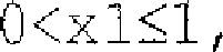




an intermediate layer formed on the red fluorescent layer, the intermediate layer being made of transparent resin, an outer circumference of the intermediate layer having a semicircular shape with a diameter D in a section perpendicular to the principal surface; and a green fluorescent layer formed on the intermediate layer, the green fluorescent layer including a green phosphor, an outer circumference of the green fluorescent layer having a semicircular shape in a section perpendicular to the principal surface. A relationship between the diameter r and the diameter D satisfies equation (2):
- Embodiments will be described below with reference to the drawings.
- As used herein, the red phosphor means a phosphor that emits light ranging from an orange color to a red color (hereinafter also collectively referred to as red color), that is, light having a peak at the wavelength of 580 to 700 nm, which is longer than the excitation light, when the phosphor is excited by the light having the wavelength of 250 nm to 500 nm, that is, the near-ultraviolet light or the blue light.
- As used herein, the green phosphor means a phosphor that emits light ranging from a blue-green color to a yellow-green color (hereinafter also collectively referred to as green color), that is, light having a peak at the wavelength of 490 to 550 nm, which is longer than the excitation light, when the phosphor is excited by light having the wavelength of 250 nit, to 500 nm, that is, the near-ultraviolet light or the blue light.
- As used herein, the "white-color light" means a concept including a light bulb color, a warm white color, a white color, a day white light, and a day light color, in which pieces of light having different wavelengths used generally in the lighting device are mixed.
- A light emitting device according to a first embodiment includes the board that includes the principal surface on which the light emitting element is mounted; the light emitting element that is mounted on the principal surface to emit the light having the wavelength of 250 nm to 500 nm; the red fluorescent layer that is formed on the light emitting element to include the red phosphor expressed by the equation. (1), the outer circumference being formed into the semicircular shape having the diameter r in the section perpendicular to the principal surface;

(In the equation (1), M is an element that is selected from IA group elements, 1.1A group elements, IIIA group elements, IIIB group elements except Al(Aliminum), rare-earth elements, and IVB group elements, xl, a, b, c, and d satisfy the following relationship.


the transparent resin intermediate layer that is formed on the red fluorescent layer, the outer circumference being formed into the semicircular shape having the diameter D in the section perpendicular to the principal surface; and the green fluorescent layer that is formed on the intermediate layer to include the green phosphor, the outer circumference being formed into the semicircular shape in the section perpendicular to the principal surface. A relationship between the diameter r and the diameter D satisfies equation (2).
- The sialon phosphor having the composition expressed by the equation (1) is a red phosphor (R). The red phosphor (R) emits the light ranging from the orange color to the red color, that is, the light having the peak at the wavelength of 580 to 700 nm, which is longer than the excitation light, when the red phosphor (R) is excited by the light having the wavelength of 250 nm to 500 nm, that is, the rear-ultraviolet light or the blue light.
- Because of the small thermal quenching, the red phosphor obtains the excellent luminous efficiency even in a high temperature region. At the same time, an excitation spectrum of the red phosphor becomes extensive from the near-ultravio.let light to the green light. Therefore, when the white-color light emitting device (white-coior LED) is formed by a combination of the red phosphor and the green phosphor, the red phosphor significantly reabsorbs the green light to possibly generate the degradation of the luminous efficiency or the color shift.
- In the light emitting device of the first embodiment, the transparent resin intermediate layer is provided between the red fluorescent layer and the green fluorescent layer, and the diameters of the red fluorescent layer and intermediate layer are restricted. Therefore, the reabsorption of the green light by the sialon red phosphor is suppressed to implement the white-color light emitting device, in which the luminous efficiency is increased and the color shift is suppressed.
-
FIG. 1 is a schematic sectional view illustrating the light emitting device of the first embodiment. Alight emitting device 10 is a white-color LED that emits the white-color light. Thelight emitting device 10 includes aboard 12 that includes the principal surface on which the light emitting element is mounted. For example, theboard 12 is made of a highly-reflective material. The principal surface means a plane in an upper surface of the board. - For example, the blue LED chip that is a
light emitting element 14 is mounted on the principal surface of theboard 12, and thelight emitting element 14 emits the light having the wavelength of 250 nm to 500 nm. For example, the blue LED chip is connected to wiring (not illustrated) through agold wire 16. Driving currents are supplied to the blue LED chip from the outside through the wiring, whereby the blue LED chip emits the blue light for excitation. - A hemispherical element sealing
transparent layer 18 made of a transparent resin is provided on thelight emitting element 14. For example, a silicone resin is used as the transparent resin. - A red
fluorescent layer 20 is formed such that the element sealingtransparent layer 18 is covered therewith. The outer circumference of the redfluorescent layer 20 is formed into the semicircular shape having the diameter r in the section perpendicular to the principal surface. The redfluorescent layer 20 includes the red phosphor having a composition expressed by the equation (1) .
(In the equation (1), M is an element that is selected from IA group elements, IIA group elements, IIIA group elements, IIIB group elements except Al, rare-earth elements, and IVB group elements. x1 a, b, c, and d satisfy the following relationship.


- Desirably, the element M is strontium (Sr).
- For example, the
red fluorescent layer 20 is formed while the red phosphor is dispersed in a transparent silicone resin. Thered fluorescent layer 20 absorbs the blue light emitted from the blue LED and converts the blue light into the red light. - J A transparent resin
intermediate layer 22 is formed on thered fluorescent layer 20. The outer circumference of theintermediate layer 22 is formed into the semicircular shape having the diameter D in the section perpendicular to the principal surface of theboard 12. For example, a silicone resin is used as the transparent resin. - A
green fluorescent layer 24 including the green phosphor is formed such that theintermediate layer 22 is covered therewith, and the outer circumference of thegreen fluorescent layer 24 is formed into the semicircular shape in the section perpendicular to the principal surface. The reabsorption by thered fluorescent layer 20 is suppressed by providing theintermediate layer 22. - For example, the
green fluorescent layer 24 is formed while the green phosphor is dispersed in the transparent silicone resin. Thegreen fluorescent layer 24 absorbs the blue light emitted from the blue LED and converts the blue light into the green light. - An outer surface transparent layer (outer surface layer) 26 made of, for example, the transparent silicone resin, is formed such that the
green fluorescent layer 24 is covered herewith. Thegreen fluorescent layer 26 has a function of suppressing total reflection of the pieces of light, which are emitted from thelight emitting element 14, thered fluorescent layer 20, and thegreen fluorescent layer 24, at an interface with an atmosphere. - Thus, the
light emitting device 10 includes thered fluorescent layer 20, intermediatetransparent layer 22 made of transparent resin, andgreen fluorescent layer 24, which are stacked into the hemispherical shape on thelight emitting element 14. Thelight emitting device 10 emits the white-color light having the high emission intensity and high coloring homogeneity by forming the fluorescent layers into the hemispherical shape. - The relationship between the diameter r outside the
red fluorescent layer 20 and the diameter D outside theintermediate layer 22 satisfies the following equation (2).
- The
red fluorescent layer 20 and theintermediate layer 22 are permitted to deviate from the perfect hemispherical shape due to factors on the production, for example. In such cases, the diameter r or the diameter D may be computed by averaging a diameter in a direction perpendicular to the principal surface of theboard 12 and a diameter in a direction parallel to the principal surface of theboard 12. - Next, function of the
light emitting device 10 will be described. -
FIG. 2 is a view illustrating normalized emission intensity of the sialon red phosphor having the composition expressed by the equation (1). InFIG. 2 , a horizontal axis indicates a wavelength of excitation light, and a vertical axis indicates the normalized emission intensity at a monitoring wavelength of 602 nm. - An absorptance of 87% at the wavelength of 457 nm is determined from an emission property evaluation when the excitation is performed by the blue LED having the peak wavelength of 457 nm. The absorptance of 68% of the green light at the wavelength of 525 nm is determined by a proportional distribution from the absorptance of 87% and the property of
FIG. 2 . Hereinafter an absorptance of the green light by the red phosphor of the first embodiment is representatively discussed by the value of 0.68. - Practically a luminous flux loss caused by the reabsorption of the green light by the
red fluorescent layer 20 is desirably set to 5% or less from the viewpoint of the property of the light emitting device. The relationship required for the diameter r outside thered fluorescent layer 20 and the diameter D outside theintermediate layer 22 will be derived in order to satisfy the condition that the luminous flux loss is 5% or less. -
FIG. 3 is an explanatory view of action of the light emitting device of the first embodiment. For example, the green light emitted from a position A in thegreen fluorescent layer 24 spread all around as illustrated inFIG. 3 . InFIG. 2 , a luminous flux in a range conceptually indicated by two arrows and a dotted-line ellipsoid, that is, a luminous f1 ax in a range where the red fluorescent layer is seen from the position A becomes a luminous flux that is possibly absorbed by thered fluorescent layer 20. - A ratio L2/Ill of a luminous flux L2 (the luminous flux that is possibly absorbed by the red fluorescent layer 20) reaching the outer surface of the
red fluorescent layer 20 to a total luminous flux L1 from thegreen fluorescent layer 24 is expressed by the following equation (4).
- A luminous flux loss y generated by the reabsorption of the green light by the
red fluorescent layer 20 is expressed by a product of the absorptance β (=0.68) of the green light by the red phosphor, the ration L2/L1, and a luminous factor differences (=0.63) between the green light (wavelength of 525 nm) and the red light (wavelength of 600 nm). That is, the luminous flux loss y is expressed by the following equation (5) .
-
FIG. 4 is a graph illustrating the luminous flux loss of the light emitting device of the first embodiment. InFIG. 4 , the horizontal axis indicates D/r, and the vertical axis indicates the luminous flux loss y computed from the equation (4) . At this pint, computation is performed using β=0.68 and δ=0. 63. - As is clear from
FIG. 4 , in order to obtain the luminous flux loss y of 5% or loss, desirably D/r is not lower than 2.0 and more desirably D/r is not lower than 2.2. Therefore, desirably the following equation (6) is satisfied. When D/r is not lower than 2.0, a tendency to saturate the luminous flux loss becomes preferably prominent.
- However, when the
intermediate layer 22 is excessively thickened, the luminous flux loss caused by the absorption by theintermediate layer 22 becomes obvious to possibly lose the effect that the diameters of thered fluorescent layer 20 andintermediate layer 22 are restricted. The silicone resin that is the typical transparent resin has a transmittance of 90% in a range of the near-ultraviolet light to the blue light with respect to a resin plate having a thickness of 2000 µm. That is, the absorptance is 10%. - It is necessary that a the thickness (D-r) of the
intermediate layer 22 satisfy the following equation (7) in order to suppress the luminous flux loss, caused by the absorption of the excitation light or the phosphor emission in theintermediate layer 22, to 5% or less.
- In order to suppress the effect of the
intermediate layer 22, desirably the thickness (D-r) of theintermediate layer 22 is 500 µm or less, more desirably the thickness (D-r) is 200 µm or less. - Accordingly, in the light emitting device, it is necessary that the diameter r outside the
red fluorescent layer 20 and the diameter D outside theintermediate layer 22 satisfies the following equation (2) :from the equation (6) and the equation (7) in order that the absorption losses by thered fluorescent layer 20 and theintermediate layer 22 is suppress to the practically-required value of 5% or less.
- Therefore, the first embodiment implements the light emitting device in which the reabsorption of the green light by the red fluorescent layeris suppressed exert the excellent luminous efficiency while the red phosphor having the small thermal quenching is used.
- In the light emitting device of the first embodiment, desirably the green phosphor has the composition expressed by the following equation (3) .

(In the equation (3), M' is an element that is selected from IA group elements, IIA group elements, IIIA group elements, IIIB group elements except Al, rare-earth elements, and IVB group elements. x2, y, z, u, and w satisfy the following relationship.


- The sialon phosphor having the composition expressed by the equation (3) is a green phosphor ( G) . The green phosphor (G) emits the light ranging from the blue-green color to the yellow-green color, that is, the light having the peak at the wavelength of 490 to 580 nm, which is longer than the excitation light, when the green phosphor (G) is excitedbythelight having the wavelength of 250 nm to 500 nm, that is, the near-ultraviolet light or the blue light.
- The green phosphor (G) has the small thermal quenching to realize the excellent luminous efficiency particularly in a high temperature region. Accordingly the high-efficiency light emitting device having the better thermal quenching property can be implemented.
- Desirably, the element M' is strontium (Sr).
- The blue LED is used in the light emitting element of the first embodiment. On the other hand, a near-ultraviolet LED is used in a light emitting element according to a second embodiment, and the light emitting device of the second embodiment includes a blue fluorescent layer. Therefore, the descriptions of the contents overlapped with those of the first embodiment are omitted.
-
FIG. 5 is a schematic sectional view illustrating the light emitting device of the second embodiment. Alight emitting device 20 is a white-color LED that emits the white-color light. In thelight emitting device 20, thelight emitting element 14 is the near-ultraviolet LED that emits near-ultraviolet light. Ablue fluorescent layer 28 is further formed between thegreen fluorescent layer 24 and the outer surfacetransparent layer 26. - For example, the
blue fluorescent layer 28 is formed while a blue phosphors is dispersed in a transparency silicone resin. Theblue fluorescent layer 28 absorbs the near-ultraviolet light emitted from the near-ultraviolet LED and converts the near-ultraviolet light into blue light. - Other configurations of the second embodiment are similar to those of the first embodiment. In the light emitting device of the second embodiment, similar to the first embodiment, the reabsorption of the green light by the red fluorescent layer is suppressed exert the excellent luminous efficiency while the red phosphor having the small thermal quenching is used.
- While certain embodiments have been described, these embodiments have been presented by way of example only, and are not intended to limit the scope of the inventions. Indeed, the light emitting device described herein may be embodied in a variety of other forms; furthermore, various omissions, substitutions and changes in the form of the devices and methods described herein may be made without departing from the spirit of the inventions. The accompanying claims and their equivalents are intended to cover such forms or modifications as would fall within the scope and spirit of the inventions.
- For example, a semiconductor light emitting element that emits the near-ultraviolet light or the blue light may be used as the light emitting element that emits the excitation light used in the light emitting device. For example, a gallium nitride compound semi conductor can be used as the LED.
- In the embodiments, the intermediate layer is directly formed on the red fluorescent layer by way of example. Alternatively, for example, a yellow fluorescent layer including a yellow phosphor may be formed between the red fluorescent layer and the intermediate layer.
- It is desirable to form the element sealing transparent layer and the outer surface transparent layer. However, it is not always necessary to form the element sealing transparent layer and the outer surface transparent layer. One of or both the element sealing transparent layer and the outer surface transparent layer may be omitted.
- Any binder resin can be used as the binder resin that constitutes the base material of the sealing resin as long as the binder resin is substantially transparent in the neighborhood of the peak wavelength of the light emitting element (excitation element) and the wavelength range longer than the peak wavelength of the light emitting element. Generally examples of the binder resin include a silicone resin, an epoxy resin, a polydimethylcyclohexan derivative having an epoxy group, an oxetane resin, an acrylic resin, a cycloolefin resin, a urea resin, a fluorine resin, and a polyimide resin.
-
FIG. 6 is a wiring diagram of a white-color light emitting module of Examples. Thelight emitting devices 10 of the first embodiment illustrated inFIG. 1 were connected so as to become a 4-by-4 array illustrated inFIG. 6 , and ananode electrode 60 and acathode electrode 62 were formed. - The sialon phosphors having compositions of TABLE 1 were applied to the red phosphor, and the sialon phosphors were expressed, by a composition formula of the following equation (8).

- The sialon phosphors having compositions of TABLE 2 were applied to the green phosphor, and the sialon phosphors were expressed by a composition formula of the following equation (9) .

- The diameter r outside the red fluorescent layer was set to 105 µm, and the diameter D outside the intermediate layer was set to 410 µm. The diameter r and the diameter D satisfy the equation (2).

- The white-color light emitting module was driven at 20 mA, and the luminous efficiency was evaluated by the total luminous flux using the integrating sphere. TABLE 3 illustrates the result.
-
[TABLE 1] x1 a b c d Peak wavelength
(nm)Example 1 0.10 0.858 3.34 0.350 4.92 622 Example 2 0.11 0.935 3.41 0.418 5.18 631 Example 3 0.15 0.911 3.70 0.272 5.63 642 Example 4 0.08 0.680 2.54 0.332 4.29 616 Example 5 0.09 0.680 2.54 0.332 4.29 616 -
[TABLE 2] x2 y z u w Peak wavelength
(nm)Example 1 0.10 -0.08 0.11 -0.04 1.43 524 Example 2 0.08 -0.06 0.13 0.22 0.06 518 Example 0.10 -0.08 -0.03 -0.06 0.09 520 Example 4 0.07 -0.07 -0.23 -0.03 0.79 511 Example 5 0.08 -0.06 -0.15 0.11 -0.11 516 - The white-color light emitting modules were produced and evaluated similarly to Examples 1 to 5 except that the green fluorescent layer was directly formed on the red fluorescent layer while the intermediate layer was not formed. TABLE 3 illustrates the result.
- The white-color light emitting modules were produced and evaluated similarly to Examples 1 to 5 except that the diameter D outside the intermediate layer was set to 2150 µm. TABLE 3 illustrates the result. The diameter r and the diameter D do not satisfy the equation (2).

-
[TABLE 3] Luminous efficiency
Examples
Comparative examplesLuminous efficiency
(1m/W)Examples 1-5 52∾54 Comparative examples 1-5 48∾50 Comparative examples 6-10 46∾48 - As is clear from TABLE 3, it is confirmed that the luminous efficiency is improved in Examples 1 to 5.
- The white-color light emitting modules were produced and evaluated similarly to Examples 1 to 5 except that an Eu activated alkaline earth orthosilicate phosphor was used as the green phosphor, the diameter r outside the red fluorescent layer was set to 120 µm, and the diameter D outside the intermediate layer was set to 505 µm. TABLE 4 illustrates the result. The diameter r and the diameter D satisfy the equation (2).

- The white-color light emitting modules were produced and evaluated similarly to Examples 6 to 10 except that the green fluorescent layer was directly formed on the red fluorescent layer while the intermediate layer was not formed. TABLE 4 illustrates the result.
- The white-color light emitting modules were produced and evaluated similarly to Examples 6 to 10 except that the diameter D outside the intermediate layer was set to 2150 µm. TABLE 4 illustrates the result. The diameter r and the diameter D do not satisfy the equation (2).

-
[TABLE 4] Luminous efficiency
(1m/W)Examples 6-10 54∼56 Comparative examples 11-15 51∾53 Comparative examples 16-20 48∾50 - As is clear from TABLE 4, it is confirmed that the luminous efficiency is improved in Examples 6 to 10.
- The
light emitting devices 20 of the second embodiment illustrated inFIG. 5 , in which the near-ultraviolet LEDs were used as the light emitting element, were connected so as to become a 4-by-4 array illustrated inFIG. 6 , and theanode electrode 60 and thecathode electrode 62 were formed. - The sialon phosphors having compositions of TABLE 1 were applied to the red phosphor, and the sialon phosphors were expressed by the composition formula of the following equation (8).

- The sialon phosphors having compositions of TABLE 2 were applied to the green phosphor, and the sialon phosphors were expressed by the composition formula of the following equation (9).

- (Sr, Ca, Ba) 10 (PO4) 6Cl2: EU24 was used as the blue phosphor.
- The diameter r outside the red fluorescent layer was set to 95 µm, and the diameter D outside intermediate layer was set to 320 µm. The diameter r and the diameter D satisfy the equation (2) .

- Similarly to Examples 1 to 5, the white-color light emitting module was driven at 20 mA, and the luminous efficiency was evaluated by the total luminous flux using the integrating sphere. TABLE 5 illustrates the result.
- The white-color light emitting modules were produced and evaluated similarly to Examples 11 to 15 except that the green fluorescent layer was directly formed on the red fluorescent layer while the intermediate layer was not formed. TABLE 5 illustrates the result.
- The white-color light emitting modules were produced and evaluated similarly to Examples 11 to 15 except that the diameter D outside the intermediate layer was set to 1850 µm. TABLE 5 illustrates the result. The diameter r and the diameter D do not satisfy the equation (2) .

-
[TABLE 5 ] Luminous efficiency
(1m/W)Examples 11-15 47∾49 Comparative examples 21-25 42∾44 Comparative examples 26-30 39∾41 - As is clear from TABLE 5, it is confirmed that the luminous efficiency is improved in Examples 11 to 15.
- The white-color light emitting modules were produced and evaluated similarly to Examples 11 to 15 except that the Eu activated alkaline earth orthosilicate phosphor was used as the green phosphor, the diameter r outside the red fluorescent layer was set to 130 µm,and the diameter D outside the intermediate layer was set to 450 µm. TABLE 6 illustrates the result. The diameter r and the diameter D satisfy the equation (2).

- The white-color light emitting modules were produced and evaluated similarly to Examples 16 to 20 except that the green fluorescent layer was directly formed on the red fluorescent layer while the intermediate layer was not formed. TABLE 6 illustrates the result.
- The white-color light emitting modules were produced and evaluated similarly to Examples 16 to 20 except that the diameter D outsiαe the intermediate layer was set to 2150 µm. TABLE 6 illustrates the result. The diameter r and the diameter D do not satisfy the equation (2).

-
[TABLE 6] Luminous efficiency
(1 m/W)Examples 16-20 47∾49 Comparative examples 31-35 41∾43 Comparative examples 36-40 37∾39 - As is clear from TABLE 6, it is confirmed that the luminous efficiency is improved in Examples 16 to 20.
Claims (9)
- A light emitting device comprising:a board;a light emitting element mounted on a principal surface of the board, the light emitting element emitting light having a wavelength of 250 nm to 500 nm;a red fluorescent layer formed on the light emitting element, the red fluorescent layer including a red phosphor expressed by equation (1), an outer circumference of the red fluorescent layer having a semicircular shape with a diameter r in a section perpendicular to the principal surface;

(In the equation (1) , M is an element that is selected from IA group elements, IIA group elements, IIIA group elements, IIIB group elements except Al (Aliminum), rare-earth elements, and IVB group elements, and x1, a, b, c, and d satisfy the following relationship:


 an intermediate layer formed on the red fluorescent layer, the intermediate layer being made of transparent resin, an outer circumference of the intermediate layer having a semicircular shape with a diameter D in a section perpendicular to the principal surface; anda green fluorescent layer formed on the intermediate layer, the green fluorescent layer including a green phosphor, an outer circumference of the green fluorescent layer having a semicircular shape in a section perpendicular to the principal surface,wherein a relationship between the diameter r and the diameter D satisfies equation (2):
- The device according to claim 1, wherein the green phosphor has a compsition expressed by equation (3):

(In the equation (3), M' is an element that is selected from IA group elements, IIA group elements, IIIA group elements, IIIB group elements except Al(Aliminum), rare-earth elements, and IVB group elements, and x2, y, z, u, and w satisfy the following relationship:


- The device according to claim 1, wherein the green phosphor is an Eu activated alkaline earth orthosilicate phosphor.
- The device according to claim 1, wherein the light emitting element is a blue LED.
- The device according to claim 1, wherein the transparent resin is a silicone resin.
- The device according to claim 1, wherein the element M is a strontium (Sr).
- The device according to claim 2, wherein the element M' is a strontium (Sr).
- The device according to claim 1, further comprising an outer surface layer made of a transparent resin, the outer surface layer being formed on the green fluorescent layer.
- The device according to claim 1, further comprising a yellow fluorescent layer including a yellow phosphor, the yellow fluorescent layer being formed between the red fluorescent layer and the intermediate layer.
Applications Claiming Priority (1)
| Application Number | Priority Date | Filing Date | Title |
|---|---|---|---|
| JP2010199983 | 2010-09-07 |
Publications (3)
| Publication Number | Publication Date |
|---|---|
| EP2426745A2 true EP2426745A2 (en) | 2012-03-07 |
| EP2426745A3 EP2426745A3 (en) | 2014-04-30 |
| EP2426745B1 EP2426745B1 (en) | 2019-10-30 |
Family
ID=45442722
Family Applications (1)
| Application Number | Title | Priority Date | Filing Date |
|---|---|---|---|
| EP11156159.3A Active EP2426745B1 (en) | 2010-09-07 | 2011-02-28 | Wavelength conversion configuration for a light emitting device |
Country Status (5)
| Country | Link |
|---|---|
| US (1) | US8436527B2 (en) |
| EP (1) | EP2426745B1 (en) |
| KR (1) | KR101408508B1 (en) |
| CN (1) | CN102403438B (en) |
| TW (1) | TWI492419B (en) |
Cited By (3)
| Publication number | Priority date | Publication date | Assignee | Title |
|---|---|---|---|---|
| EP2787055A1 (en) * | 2013-04-03 | 2014-10-08 | Kabushiki Kaisha Toshiba | Light emitting device |
| EP2843299A1 (en) * | 2013-09-03 | 2015-03-04 | Panasonic Corporation | Light source device |
| CN109020558A (en) * | 2018-09-07 | 2018-12-18 | 安徽理工大学 | A kind of high-power warm white solid-state lighting SiAlON fluorescent transparent ceramics and preparation method thereof |
Families Citing this family (15)
| Publication number | Priority date | Publication date | Assignee | Title |
|---|---|---|---|---|
| JP5592602B2 (en) * | 2008-07-31 | 2014-09-17 | 株式会社東芝 | Phosphor and light emitting device using the same |
| JP4929413B2 (en) * | 2010-09-07 | 2012-05-09 | 株式会社東芝 | Light emitting device |
| US8414795B2 (en) * | 2010-09-09 | 2013-04-09 | Kabushiki Kaisha Toshiba | Red light-emitting fluorescent substance and light-emitting device employing the same |
| JP5185421B2 (en) * | 2010-09-09 | 2013-04-17 | 株式会社東芝 | Red light emitting phosphor and light emitting device using the same |
| WO2012123841A1 (en) * | 2011-03-16 | 2012-09-20 | Koninklijke Philips Electronics N.V. | A lighting device, a lamp and a luminaire |
| EP3078903B1 (en) * | 2011-09-08 | 2018-04-11 | LG Innotek Co., Ltd. | Lighting module |
| US9365766B2 (en) * | 2011-10-13 | 2016-06-14 | Intematix Corporation | Wavelength conversion component having photo-luminescence material embedded into a hermetic material for remote wavelength conversion |
| JP5893888B2 (en) * | 2011-10-13 | 2016-03-23 | シチズン電子株式会社 | Semiconductor light emitting device |
| WO2015056525A1 (en) * | 2013-10-18 | 2015-04-23 | シャープ株式会社 | Light-emitting device |
| JP2015211202A (en) * | 2014-04-30 | 2015-11-24 | 株式会社東芝 | Light emitting device |
| JP6428089B2 (en) * | 2014-09-24 | 2018-11-28 | 日亜化学工業株式会社 | Light emitting device |
| US10784416B2 (en) * | 2016-03-24 | 2020-09-22 | Sharp Kabushiki Kaisha | Light source device and light emitting device |
| CN105911766A (en) * | 2016-06-16 | 2016-08-31 | 青岛海信电器股份有限公司 | Quantum dot light-emitting device, backlight module and liquid crystal display device |
| US10203547B2 (en) | 2016-06-16 | 2019-02-12 | Hisense Electric Co., Ltd. | Quantum dot light emitting device, backlight module, and liquid crystal display device |
| CN108417701B (en) * | 2018-01-24 | 2020-04-03 | 厦门信达光电物联科技研究院有限公司 | Preparation method of white light LED healthy light source |
Citations (1)
| Publication number | Priority date | Publication date | Assignee | Title |
|---|---|---|---|---|
| JP2010199983A (en) | 2009-02-25 | 2010-09-09 | Fuji Xerox Co Ltd | Image processor, image reader and image forming apparatus |
Family Cites Families (13)
| Publication number | Priority date | Publication date | Assignee | Title |
|---|---|---|---|---|
| JP3614776B2 (en) * | 2000-12-19 | 2005-01-26 | シャープ株式会社 | Chip component type LED and its manufacturing method |
| US7452737B2 (en) * | 2004-11-15 | 2008-11-18 | Philips Lumileds Lighting Company, Llc | Molded lens over LED die |
| WO2007105631A1 (en) | 2006-03-10 | 2007-09-20 | Kabushiki Kaisha Toshiba | Phosphor and light-emitting device |
| JP2007273562A (en) | 2006-03-30 | 2007-10-18 | Toshiba Corp | Semiconductor light emitting device |
| JP5044329B2 (en) | 2007-08-31 | 2012-10-10 | 株式会社東芝 | Light emitting device |
| KR101156898B1 (en) * | 2007-09-21 | 2012-06-21 | 도시바 마테리알 가부시키가이샤 | White light-emitting lamp for illumination and illuminating device using the same |
| BRPI0913195A2 (en) * | 2008-05-30 | 2016-01-12 | Sharp Kk | light emitting device, surface light source, liquid crystal display device and method for manufacturing light emitting device |
| JP5592602B2 (en) | 2008-07-31 | 2014-09-17 | 株式会社東芝 | Phosphor and light emitting device using the same |
| JP5243883B2 (en) * | 2008-08-06 | 2013-07-24 | パナソニック株式会社 | Light emitting device and lighting apparatus |
| JP4881358B2 (en) | 2008-08-28 | 2012-02-22 | 株式会社東芝 | Light emitting device |
| JP4869317B2 (en) | 2008-10-29 | 2012-02-08 | 株式会社東芝 | Red phosphor and light emitting device using the same |
| JP5226774B2 (en) * | 2009-07-27 | 2013-07-03 | 株式会社東芝 | Light emitting device |
| EP2428543B1 (en) * | 2010-09-08 | 2013-05-08 | Kabushiki Kaisha Toshiba | Light emitting device |
-
2011
- 2011-02-24 US US13/034,137 patent/US8436527B2/en not_active Expired - Fee Related
- 2011-02-25 KR KR1020110017218A patent/KR101408508B1/en not_active Expired - Fee Related
- 2011-02-28 EP EP11156159.3A patent/EP2426745B1/en active Active
- 2011-03-03 CN CN201110050912.6A patent/CN102403438B/en not_active Expired - Fee Related
- 2011-03-03 TW TW100107161A patent/TWI492419B/en not_active IP Right Cessation
Patent Citations (1)
| Publication number | Priority date | Publication date | Assignee | Title |
|---|---|---|---|---|
| JP2010199983A (en) | 2009-02-25 | 2010-09-09 | Fuji Xerox Co Ltd | Image processor, image reader and image forming apparatus |
Cited By (7)
| Publication number | Priority date | Publication date | Assignee | Title |
|---|---|---|---|---|
| EP2787055A1 (en) * | 2013-04-03 | 2014-10-08 | Kabushiki Kaisha Toshiba | Light emitting device |
| CN104103743A (en) * | 2013-04-03 | 2014-10-15 | 株式会社东芝 | Light emitting device |
| US9190582B2 (en) | 2013-04-03 | 2015-11-17 | Kabushiki Kaisha Toshiba | Light emitting device |
| EP2843299A1 (en) * | 2013-09-03 | 2015-03-04 | Panasonic Corporation | Light source device |
| US9142733B2 (en) | 2013-09-03 | 2015-09-22 | Panasonic Intellectual Property Management Co., Ltd. | Light source device including a high energy light source and a wavelength conversion member, illuminating device comprising the same, and vehicle |
| CN109020558A (en) * | 2018-09-07 | 2018-12-18 | 安徽理工大学 | A kind of high-power warm white solid-state lighting SiAlON fluorescent transparent ceramics and preparation method thereof |
| CN109020558B (en) * | 2018-09-07 | 2021-11-12 | 安徽理工大学 | SiAlON fluorescent transparent ceramic for high-power warm white light solid-state lighting and preparation method thereof |
Also Published As
| Publication number | Publication date |
|---|---|
| US20120056527A1 (en) | 2012-03-08 |
| KR20120025367A (en) | 2012-03-15 |
| TW201212293A (en) | 2012-03-16 |
| EP2426745A3 (en) | 2014-04-30 |
| US8436527B2 (en) | 2013-05-07 |
| TWI492419B (en) | 2015-07-11 |
| CN102403438B (en) | 2014-09-10 |
| EP2426745B1 (en) | 2019-10-30 |
| CN102403438A (en) | 2012-04-04 |
| KR101408508B1 (en) | 2014-06-17 |
Similar Documents
| Publication | Publication Date | Title |
|---|---|---|
| EP2426745B1 (en) | Wavelength conversion configuration for a light emitting device | |
| EP2428543B1 (en) | Light emitting device | |
| JP3223302U (en) | LED light emitting device | |
| KR100549906B1 (en) | Light emitting device | |
| CN103069582B (en) | Systems and methods for selectively pumping LEDs with multiple phosphors | |
| US8414145B2 (en) | Light emitting device | |
| US8921878B2 (en) | Light emitting device | |
| US8299701B2 (en) | Lighting device having illumination, backlighting and display applications | |
| US8471277B2 (en) | Light emitting device | |
| JP2010080935A (en) | Semiconductor light emitting device, backlight source using the same, backlight source system, display, and electronic apparatus | |
| EP2975100B1 (en) | Yellow light emitting phosphor and light emitting device package using the same | |
| JP2005093985A (en) | Method of producing white light by secondary excitation method and its white light emitting device | |
| WO2006135005A1 (en) | Light emitting device | |
| US8546824B2 (en) | Light emitting device | |
| JP2008546196A (en) | Lighting system with luminescent material to compensate for color shortage | |
| US10150912B2 (en) | Red phosphor, white light emitting apparatus, display apparatus, and lighting apparatus | |
| JP5066786B2 (en) | Nitride phosphor and light emitting device using the same | |
| US7999274B2 (en) | White light emitting device | |
| JP2018533210A (en) | Optoelectronic components, background lighting for displays, and methods of manufacturing optoelectronic components | |
| JP5868929B2 (en) | Phosphor composition and light emitting device package including the same | |
| US20120057338A1 (en) | Light emitting device | |
| WO2020066839A1 (en) | Warm-color complex phosphor, wavelength conversion body, and light emitting device | |
| KR102035169B1 (en) | Phosphor compositions | |
| KR200400564Y1 (en) | White light emitting device | |
| EP1726631A1 (en) | White light emitting device |
Legal Events
| Date | Code | Title | Description |
|---|---|---|---|
| 17P | Request for examination filed |
Effective date: 20110228 |
|
| AK | Designated contracting states |
Kind code of ref document: A2 Designated state(s): AL AT BE BG CH CY CZ DE DK EE ES FI FR GB GR HR HU IE IS IT LI LT LU LV MC MK MT NL NO PL PT RO RS SE SI SK SM TR |
|
| AX | Request for extension of the european patent |
Extension state: BA ME |
|
| PUAI | Public reference made under article 153(3) epc to a published international application that has entered the european phase |
Free format text: ORIGINAL CODE: 0009012 |
|
| PUAL | Search report despatched |
Free format text: ORIGINAL CODE: 0009013 |
|
| AK | Designated contracting states |
Kind code of ref document: A3 Designated state(s): AL AT BE BG CH CY CZ DE DK EE ES FI FR GB GR HR HU IE IS IT LI LT LU LV MC MK MT NL NO PL PT RO RS SE SI SK SM TR |
|
| AX | Request for extension of the european patent |
Extension state: BA ME |
|
| RIC1 | Information provided on ipc code assigned before grant |
Ipc: C09K 11/55 20060101ALI20140327BHEP Ipc: H05B 33/14 20060101ALI20140327BHEP Ipc: C09K 11/08 20060101AFI20140327BHEP Ipc: C09K 11/77 20060101ALI20140327BHEP Ipc: H01L 25/075 20060101ALN20140327BHEP Ipc: H01L 33/56 20100101ALN20140327BHEP Ipc: H01L 33/50 20100101ALI20140327BHEP |
|
| RAP1 | Party data changed (applicant data changed or rights of an application transferred) |
Owner name: ALPAD CORPORATION |
|
| GRAP | Despatch of communication of intention to grant a patent |
Free format text: ORIGINAL CODE: EPIDOSNIGR1 |
|
| STAA | Information on the status of an ep patent application or granted ep patent |
Free format text: STATUS: GRANT OF PATENT IS INTENDED |
|
| INTG | Intention to grant announced |
Effective date: 20190403 |
|
| GRAJ | Information related to disapproval of communication of intention to grant by the applicant or resumption of examination proceedings by the epo deleted |
Free format text: ORIGINAL CODE: EPIDOSDIGR1 |
|
| STAA | Information on the status of an ep patent application or granted ep patent |
Free format text: STATUS: REQUEST FOR EXAMINATION WAS MADE |
|
| INTC | Intention to grant announced (deleted) | ||
| GRAR | Information related to intention to grant a patent recorded |
Free format text: ORIGINAL CODE: EPIDOSNIGR71 |
|
| GRAS | Grant fee paid |
Free format text: ORIGINAL CODE: EPIDOSNIGR3 |
|
| STAA | Information on the status of an ep patent application or granted ep patent |
Free format text: STATUS: GRANT OF PATENT IS INTENDED |
|
| GRAA | (expected) grant |
Free format text: ORIGINAL CODE: 0009210 |
|
| STAA | Information on the status of an ep patent application or granted ep patent |
Free format text: STATUS: THE PATENT HAS BEEN GRANTED |
|
| AK | Designated contracting states |
Kind code of ref document: B1 Designated state(s): AL AT BE BG CH CY CZ DE DK EE ES FI FR GB GR HR HU IE IS IT LI LT LU LV MC MK MT NL NO PL PT RO RS SE SI SK SM TR |
|
| INTG | Intention to grant announced |
Effective date: 20190920 |
|
| REG | Reference to a national code |
Ref country code: GB Ref legal event code: FG4D |
|
| REG | Reference to a national code |
Ref country code: CH Ref legal event code: EP |
|
| REG | Reference to a national code |
Ref country code: AT Ref legal event code: REF Ref document number: 1196125 Country of ref document: AT Kind code of ref document: T Effective date: 20191115 |
|
| REG | Reference to a national code |
Ref country code: DE Ref legal event code: R096 Ref document number: 602011063007 Country of ref document: DE |
|
| REG | Reference to a national code |
Ref country code: IE Ref legal event code: FG4D |
|
| REG | Reference to a national code |
Ref country code: LT Ref legal event code: MG4D |
|
| PG25 | Lapsed in a contracting state [announced via postgrant information from national office to epo] |
Ref country code: PT Free format text: LAPSE BECAUSE OF FAILURE TO SUBMIT A TRANSLATION OF THE DESCRIPTION OR TO PAY THE FEE WITHIN THE PRESCRIBED TIME-LIMIT Effective date: 20200302 Ref country code: NO Free format text: LAPSE BECAUSE OF FAILURE TO SUBMIT A TRANSLATION OF THE DESCRIPTION OR TO PAY THE FEE WITHIN THE PRESCRIBED TIME-LIMIT Effective date: 20200130 Ref country code: FI Free format text: LAPSE BECAUSE OF FAILURE TO SUBMIT A TRANSLATION OF THE DESCRIPTION OR TO PAY THE FEE WITHIN THE PRESCRIBED TIME-LIMIT Effective date: 20191030 Ref country code: BG Free format text: LAPSE BECAUSE OF FAILURE TO SUBMIT A TRANSLATION OF THE DESCRIPTION OR TO PAY THE FEE WITHIN THE PRESCRIBED TIME-LIMIT Effective date: 20200130 Ref country code: LV Free format text: LAPSE BECAUSE OF FAILURE TO SUBMIT A TRANSLATION OF THE DESCRIPTION OR TO PAY THE FEE WITHIN THE PRESCRIBED TIME-LIMIT Effective date: 20191030 Ref country code: SE Free format text: LAPSE BECAUSE OF FAILURE TO SUBMIT A TRANSLATION OF THE DESCRIPTION OR TO PAY THE FEE WITHIN THE PRESCRIBED TIME-LIMIT Effective date: 20191030 Ref country code: NL Free format text: LAPSE BECAUSE OF FAILURE TO SUBMIT A TRANSLATION OF THE DESCRIPTION OR TO PAY THE FEE WITHIN THE PRESCRIBED TIME-LIMIT Effective date: 20191030 Ref country code: PL Free format text: LAPSE BECAUSE OF FAILURE TO SUBMIT A TRANSLATION OF THE DESCRIPTION OR TO PAY THE FEE WITHIN THE PRESCRIBED TIME-LIMIT Effective date: 20191030 Ref country code: GR Free format text: LAPSE BECAUSE OF FAILURE TO SUBMIT A TRANSLATION OF THE DESCRIPTION OR TO PAY THE FEE WITHIN THE PRESCRIBED TIME-LIMIT Effective date: 20200131 Ref country code: ES Free format text: LAPSE BECAUSE OF FAILURE TO SUBMIT A TRANSLATION OF THE DESCRIPTION OR TO PAY THE FEE WITHIN THE PRESCRIBED TIME-LIMIT Effective date: 20191030 Ref country code: LT Free format text: LAPSE BECAUSE OF FAILURE TO SUBMIT A TRANSLATION OF THE DESCRIPTION OR TO PAY THE FEE WITHIN THE PRESCRIBED TIME-LIMIT Effective date: 20191030 |
|
| REG | Reference to a national code |
Ref country code: NL Ref legal event code: MP Effective date: 20191030 |
|
| PG25 | Lapsed in a contracting state [announced via postgrant information from national office to epo] |
Ref country code: HR Free format text: LAPSE BECAUSE OF FAILURE TO SUBMIT A TRANSLATION OF THE DESCRIPTION OR TO PAY THE FEE WITHIN THE PRESCRIBED TIME-LIMIT Effective date: 20191030 Ref country code: IS Free format text: LAPSE BECAUSE OF FAILURE TO SUBMIT A TRANSLATION OF THE DESCRIPTION OR TO PAY THE FEE WITHIN THE PRESCRIBED TIME-LIMIT Effective date: 20200229 Ref country code: RS Free format text: LAPSE BECAUSE OF FAILURE TO SUBMIT A TRANSLATION OF THE DESCRIPTION OR TO PAY THE FEE WITHIN THE PRESCRIBED TIME-LIMIT Effective date: 20191030 |
|
| PG25 | Lapsed in a contracting state [announced via postgrant information from national office to epo] |
Ref country code: AL Free format text: LAPSE BECAUSE OF FAILURE TO SUBMIT A TRANSLATION OF THE DESCRIPTION OR TO PAY THE FEE WITHIN THE PRESCRIBED TIME-LIMIT Effective date: 20191030 |
|
| PG25 | Lapsed in a contracting state [announced via postgrant information from national office to epo] |
Ref country code: DK Free format text: LAPSE BECAUSE OF FAILURE TO SUBMIT A TRANSLATION OF THE DESCRIPTION OR TO PAY THE FEE WITHIN THE PRESCRIBED TIME-LIMIT Effective date: 20191030 Ref country code: EE Free format text: LAPSE BECAUSE OF FAILURE TO SUBMIT A TRANSLATION OF THE DESCRIPTION OR TO PAY THE FEE WITHIN THE PRESCRIBED TIME-LIMIT Effective date: 20191030 Ref country code: CZ Free format text: LAPSE BECAUSE OF FAILURE TO SUBMIT A TRANSLATION OF THE DESCRIPTION OR TO PAY THE FEE WITHIN THE PRESCRIBED TIME-LIMIT Effective date: 20191030 Ref country code: RO Free format text: LAPSE BECAUSE OF FAILURE TO SUBMIT A TRANSLATION OF THE DESCRIPTION OR TO PAY THE FEE WITHIN THE PRESCRIBED TIME-LIMIT Effective date: 20191030 |
|
| REG | Reference to a national code |
Ref country code: DE Ref legal event code: R097 Ref document number: 602011063007 Country of ref document: DE |
|
| REG | Reference to a national code |
Ref country code: AT Ref legal event code: MK05 Ref document number: 1196125 Country of ref document: AT Kind code of ref document: T Effective date: 20191030 |
|
| PG25 | Lapsed in a contracting state [announced via postgrant information from national office to epo] |
Ref country code: SM Free format text: LAPSE BECAUSE OF FAILURE TO SUBMIT A TRANSLATION OF THE DESCRIPTION OR TO PAY THE FEE WITHIN THE PRESCRIBED TIME-LIMIT Effective date: 20191030 Ref country code: IT Free format text: LAPSE BECAUSE OF FAILURE TO SUBMIT A TRANSLATION OF THE DESCRIPTION OR TO PAY THE FEE WITHIN THE PRESCRIBED TIME-LIMIT Effective date: 20191030 Ref country code: SK Free format text: LAPSE BECAUSE OF FAILURE TO SUBMIT A TRANSLATION OF THE DESCRIPTION OR TO PAY THE FEE WITHIN THE PRESCRIBED TIME-LIMIT Effective date: 20191030 |
|
| PLBE | No opposition filed within time limit |
Free format text: ORIGINAL CODE: 0009261 |
|
| STAA | Information on the status of an ep patent application or granted ep patent |
Free format text: STATUS: NO OPPOSITION FILED WITHIN TIME LIMIT |
|
| REG | Reference to a national code |
Ref country code: CH Ref legal event code: PL |
|
| 26N | No opposition filed |
Effective date: 20200731 |
|
| REG | Reference to a national code |
Ref country code: BE Ref legal event code: MM Effective date: 20200229 |
|
| PG25 | Lapsed in a contracting state [announced via postgrant information from national office to epo] |
Ref country code: LU Free format text: LAPSE BECAUSE OF NON-PAYMENT OF DUE FEES Effective date: 20200228 Ref country code: MC Free format text: LAPSE BECAUSE OF FAILURE TO SUBMIT A TRANSLATION OF THE DESCRIPTION OR TO PAY THE FEE WITHIN THE PRESCRIBED TIME-LIMIT Effective date: 20191030 |
|
| PG25 | Lapsed in a contracting state [announced via postgrant information from national office to epo] |
Ref country code: CH Free format text: LAPSE BECAUSE OF NON-PAYMENT OF DUE FEES Effective date: 20200229 Ref country code: LI Free format text: LAPSE BECAUSE OF NON-PAYMENT OF DUE FEES Effective date: 20200229 Ref country code: AT Free format text: LAPSE BECAUSE OF FAILURE TO SUBMIT A TRANSLATION OF THE DESCRIPTION OR TO PAY THE FEE WITHIN THE PRESCRIBED TIME-LIMIT Effective date: 20191030 Ref country code: SI Free format text: LAPSE BECAUSE OF FAILURE TO SUBMIT A TRANSLATION OF THE DESCRIPTION OR TO PAY THE FEE WITHIN THE PRESCRIBED TIME-LIMIT Effective date: 20191030 |
|
| PG25 | Lapsed in a contracting state [announced via postgrant information from national office to epo] |
Ref country code: IE Free format text: LAPSE BECAUSE OF NON-PAYMENT OF DUE FEES Effective date: 20200228 |
|
| PG25 | Lapsed in a contracting state [announced via postgrant information from national office to epo] |
Ref country code: BE Free format text: LAPSE BECAUSE OF NON-PAYMENT OF DUE FEES Effective date: 20200229 |
|
| PG25 | Lapsed in a contracting state [announced via postgrant information from national office to epo] |
Ref country code: TR Free format text: LAPSE BECAUSE OF FAILURE TO SUBMIT A TRANSLATION OF THE DESCRIPTION OR TO PAY THE FEE WITHIN THE PRESCRIBED TIME-LIMIT Effective date: 20191030 Ref country code: MT Free format text: LAPSE BECAUSE OF FAILURE TO SUBMIT A TRANSLATION OF THE DESCRIPTION OR TO PAY THE FEE WITHIN THE PRESCRIBED TIME-LIMIT Effective date: 20191030 Ref country code: CY Free format text: LAPSE BECAUSE OF FAILURE TO SUBMIT A TRANSLATION OF THE DESCRIPTION OR TO PAY THE FEE WITHIN THE PRESCRIBED TIME-LIMIT Effective date: 20191030 |
|
| PG25 | Lapsed in a contracting state [announced via postgrant information from national office to epo] |
Ref country code: MK Free format text: LAPSE BECAUSE OF FAILURE TO SUBMIT A TRANSLATION OF THE DESCRIPTION OR TO PAY THE FEE WITHIN THE PRESCRIBED TIME-LIMIT Effective date: 20191030 |
|
| PGFP | Annual fee paid to national office [announced via postgrant information from national office to epo] |
Ref country code: FR Payment date: 20230110 Year of fee payment: 13 |
|
| PGFP | Annual fee paid to national office [announced via postgrant information from national office to epo] |
Ref country code: GB Payment date: 20230105 Year of fee payment: 13 Ref country code: DE Payment date: 20221230 Year of fee payment: 13 |
|
| REG | Reference to a national code |
Ref country code: DE Ref legal event code: R119 Ref document number: 602011063007 Country of ref document: DE |
|
| GBPC | Gb: european patent ceased through non-payment of renewal fee |
Effective date: 20240228 |
|
| PG25 | Lapsed in a contracting state [announced via postgrant information from national office to epo] |
Ref country code: DE Free format text: LAPSE BECAUSE OF NON-PAYMENT OF DUE FEES Effective date: 20240903 |
|
| PG25 | Lapsed in a contracting state [announced via postgrant information from national office to epo] |
Ref country code: GB Free format text: LAPSE BECAUSE OF NON-PAYMENT OF DUE FEES Effective date: 20240228 |
|
| PG25 | Lapsed in a contracting state [announced via postgrant information from national office to epo] |
Ref country code: FR Free format text: LAPSE BECAUSE OF NON-PAYMENT OF DUE FEES Effective date: 20240229 |
|
| PG25 | Lapsed in a contracting state [announced via postgrant information from national office to epo] |
Ref country code: GB Free format text: LAPSE BECAUSE OF NON-PAYMENT OF DUE FEES Effective date: 20240228 Ref country code: FR Free format text: LAPSE BECAUSE OF NON-PAYMENT OF DUE FEES Effective date: 20240229 Ref country code: DE Free format text: LAPSE BECAUSE OF NON-PAYMENT OF DUE FEES Effective date: 20240903 |