EP2426699B1 - Growth of multi-layer group III-nitride buffers on large-area silicon substrates and other substrates - Google Patents
Growth of multi-layer group III-nitride buffers on large-area silicon substrates and other substrates Download PDFInfo
- Publication number
- EP2426699B1 EP2426699B1 EP11178555.6A EP11178555A EP2426699B1 EP 2426699 B1 EP2426699 B1 EP 2426699B1 EP 11178555 A EP11178555 A EP 11178555A EP 2426699 B1 EP2426699 B1 EP 2426699B1
- Authority
- EP
- European Patent Office
- Prior art keywords
- layer
- epitaxial
- regions
- nitride
- group iii
- Prior art date
- Legal status (The legal status is an assumption and is not a legal conclusion. Google has not performed a legal analysis and makes no representation as to the accuracy of the status listed.)
- Active
Links
- 239000000872 buffer Substances 0.000 title claims description 67
- 239000000758 substrate Substances 0.000 title claims description 48
- XUIMIQQOPSSXEZ-UHFFFAOYSA-N Silicon Chemical compound [Si] XUIMIQQOPSSXEZ-UHFFFAOYSA-N 0.000 title description 17
- 229910052710 silicon Inorganic materials 0.000 title description 17
- 239000010703 silicon Substances 0.000 title description 17
- 239000004065 semiconductor Substances 0.000 claims description 49
- 238000000034 method Methods 0.000 claims description 33
- 238000005530 etching Methods 0.000 claims description 16
- 238000000151 deposition Methods 0.000 claims description 8
- 239000003989 dielectric material Substances 0.000 claims description 5
- 239000000463 material Substances 0.000 description 21
- JMASRVWKEDWRBT-UHFFFAOYSA-N Gallium nitride Chemical compound [Ga]#N JMASRVWKEDWRBT-UHFFFAOYSA-N 0.000 description 19
- 229910002601 GaN Inorganic materials 0.000 description 17
- 235000012431 wafers Nutrition 0.000 description 15
- 230000006911 nucleation Effects 0.000 description 9
- 238000010899 nucleation Methods 0.000 description 9
- VYPSYNLAJGMNEJ-UHFFFAOYSA-N Silicium dioxide Chemical compound O=[Si]=O VYPSYNLAJGMNEJ-UHFFFAOYSA-N 0.000 description 6
- 230000015556 catabolic process Effects 0.000 description 6
- 238000001451 molecular beam epitaxy Methods 0.000 description 6
- 238000005336 cracking Methods 0.000 description 5
- 238000004519 manufacturing process Methods 0.000 description 5
- IJGRMHOSHXDMSA-UHFFFAOYSA-N Atomic nitrogen Chemical compound N#N IJGRMHOSHXDMSA-UHFFFAOYSA-N 0.000 description 4
- 230000008021 deposition Effects 0.000 description 4
- 229910052751 metal Inorganic materials 0.000 description 4
- 239000002184 metal Substances 0.000 description 4
- 230000015572 biosynthetic process Effects 0.000 description 3
- 238000002955 isolation Methods 0.000 description 3
- 230000009467 reduction Effects 0.000 description 3
- 239000000377 silicon dioxide Substances 0.000 description 3
- AUCDRFABNLOFRE-UHFFFAOYSA-N alumane;indium Chemical compound [AlH3].[In] AUCDRFABNLOFRE-UHFFFAOYSA-N 0.000 description 2
- 230000007547 defect Effects 0.000 description 2
- 230000005669 field effect Effects 0.000 description 2
- 239000007943 implant Substances 0.000 description 2
- 229910052738 indium Inorganic materials 0.000 description 2
- APFVFJFRJDLVQX-UHFFFAOYSA-N indium atom Chemical compound [In] APFVFJFRJDLVQX-UHFFFAOYSA-N 0.000 description 2
- 150000004767 nitrides Chemical class 0.000 description 2
- 229910052757 nitrogen Inorganic materials 0.000 description 2
- 238000000059 patterning Methods 0.000 description 2
- 229910052594 sapphire Inorganic materials 0.000 description 2
- 239000010980 sapphire Substances 0.000 description 2
- HBMJWWWQQXIZIP-UHFFFAOYSA-N silicon carbide Chemical compound [Si+]#[C-] HBMJWWWQQXIZIP-UHFFFAOYSA-N 0.000 description 2
- 229910010271 silicon carbide Inorganic materials 0.000 description 2
- PIGFYZPCRLYGLF-UHFFFAOYSA-N Aluminum nitride Chemical compound [Al]#N PIGFYZPCRLYGLF-UHFFFAOYSA-N 0.000 description 1
- GYHNNYVSQQEPJS-UHFFFAOYSA-N Gallium Chemical compound [Ga] GYHNNYVSQQEPJS-UHFFFAOYSA-N 0.000 description 1
- 230000002411 adverse Effects 0.000 description 1
- 229910052782 aluminium Inorganic materials 0.000 description 1
- XAGFODPZIPBFFR-UHFFFAOYSA-N aluminium Chemical compound [Al] XAGFODPZIPBFFR-UHFFFAOYSA-N 0.000 description 1
- RNQKDQAVIXDKAG-UHFFFAOYSA-N aluminum gallium Chemical compound [Al].[Ga] RNQKDQAVIXDKAG-UHFFFAOYSA-N 0.000 description 1
- NWAIGJYBQQYSPW-UHFFFAOYSA-N azanylidyneindigane Chemical compound [In]#N NWAIGJYBQQYSPW-UHFFFAOYSA-N 0.000 description 1
- 238000005229 chemical vapour deposition Methods 0.000 description 1
- 238000004891 communication Methods 0.000 description 1
- 150000001875 compounds Chemical class 0.000 description 1
- 239000004020 conductor Substances 0.000 description 1
- 238000007796 conventional method Methods 0.000 description 1
- PMHQVHHXPFUNSP-UHFFFAOYSA-M copper(1+);methylsulfanylmethane;bromide Chemical compound Br[Cu].CSC PMHQVHHXPFUNSP-UHFFFAOYSA-M 0.000 description 1
- 230000008878 coupling Effects 0.000 description 1
- 238000010168 coupling process Methods 0.000 description 1
- 238000005859 coupling reaction Methods 0.000 description 1
- 230000001419 dependent effect Effects 0.000 description 1
- 239000002019 doping agent Substances 0.000 description 1
- 229910052733 gallium Inorganic materials 0.000 description 1
- 238000005468 ion implantation Methods 0.000 description 1
- 229910044991 metal oxide Inorganic materials 0.000 description 1
- 150000004706 metal oxides Chemical class 0.000 description 1
- 235000012239 silicon dioxide Nutrition 0.000 description 1
- 239000000126 substance Substances 0.000 description 1
Images


Classifications
-
- H—ELECTRICITY
- H01—ELECTRIC ELEMENTS
- H01L—SEMICONDUCTOR DEVICES NOT COVERED BY CLASS H10
- H01L21/00—Processes or apparatus adapted for the manufacture or treatment of semiconductor or solid state devices or of parts thereof
- H01L21/02—Manufacture or treatment of semiconductor devices or of parts thereof
- H01L21/02104—Forming layers
- H01L21/02365—Forming inorganic semiconducting materials on a substrate
- H01L21/02367—Substrates
- H01L21/0237—Materials
-
- H—ELECTRICITY
- H01—ELECTRIC ELEMENTS
- H01L—SEMICONDUCTOR DEVICES NOT COVERED BY CLASS H10
- H01L21/00—Processes or apparatus adapted for the manufacture or treatment of semiconductor or solid state devices or of parts thereof
- H01L21/70—Manufacture or treatment of devices consisting of a plurality of solid state components formed in or on a common substrate or of parts thereof; Manufacture of integrated circuit devices or of parts thereof
- H01L21/71—Manufacture of specific parts of devices defined in group H01L21/70
- H01L21/76—Making of isolation regions between components
- H01L21/762—Dielectric regions, e.g. EPIC dielectric isolation, LOCOS; Trench refilling techniques, SOI technology, use of channel stoppers
-
- H—ELECTRICITY
- H01—ELECTRIC ELEMENTS
- H01L—SEMICONDUCTOR DEVICES NOT COVERED BY CLASS H10
- H01L21/00—Processes or apparatus adapted for the manufacture or treatment of semiconductor or solid state devices or of parts thereof
- H01L21/02—Manufacture or treatment of semiconductor devices or of parts thereof
- H01L21/02104—Forming layers
- H01L21/02365—Forming inorganic semiconducting materials on a substrate
- H01L21/02367—Substrates
- H01L21/0237—Materials
- H01L21/02373—Group 14 semiconducting materials
- H01L21/02381—Silicon, silicon germanium, germanium
-
- H—ELECTRICITY
- H01—ELECTRIC ELEMENTS
- H01L—SEMICONDUCTOR DEVICES NOT COVERED BY CLASS H10
- H01L21/00—Processes or apparatus adapted for the manufacture or treatment of semiconductor or solid state devices or of parts thereof
- H01L21/02—Manufacture or treatment of semiconductor devices or of parts thereof
- H01L21/02104—Forming layers
- H01L21/02365—Forming inorganic semiconducting materials on a substrate
- H01L21/02436—Intermediate layers between substrates and deposited layers
- H01L21/02439—Materials
- H01L21/02455—Group 13/15 materials
- H01L21/02458—Nitrides
-
- H—ELECTRICITY
- H01—ELECTRIC ELEMENTS
- H01L—SEMICONDUCTOR DEVICES NOT COVERED BY CLASS H10
- H01L21/00—Processes or apparatus adapted for the manufacture or treatment of semiconductor or solid state devices or of parts thereof
- H01L21/02—Manufacture or treatment of semiconductor devices or of parts thereof
- H01L21/02104—Forming layers
- H01L21/02365—Forming inorganic semiconducting materials on a substrate
- H01L21/02436—Intermediate layers between substrates and deposited layers
- H01L21/02494—Structure
- H01L21/02496—Layer structure
- H01L21/02502—Layer structure consisting of two layers
-
- H—ELECTRICITY
- H01—ELECTRIC ELEMENTS
- H01L—SEMICONDUCTOR DEVICES NOT COVERED BY CLASS H10
- H01L21/00—Processes or apparatus adapted for the manufacture or treatment of semiconductor or solid state devices or of parts thereof
- H01L21/02—Manufacture or treatment of semiconductor devices or of parts thereof
- H01L21/02104—Forming layers
- H01L21/02365—Forming inorganic semiconducting materials on a substrate
- H01L21/02518—Deposited layers
- H01L21/02521—Materials
- H01L21/02538—Group 13/15 materials
- H01L21/0254—Nitrides
-
- H—ELECTRICITY
- H01—ELECTRIC ELEMENTS
- H01L—SEMICONDUCTOR DEVICES NOT COVERED BY CLASS H10
- H01L21/00—Processes or apparatus adapted for the manufacture or treatment of semiconductor or solid state devices or of parts thereof
- H01L21/02—Manufacture or treatment of semiconductor devices or of parts thereof
- H01L21/02104—Forming layers
- H01L21/02365—Forming inorganic semiconducting materials on a substrate
- H01L21/02612—Formation types
- H01L21/02617—Deposition types
- H01L21/02636—Selective deposition, e.g. simultaneous growth of mono- and non-monocrystalline semiconductor materials
- H01L21/02639—Preparation of substrate for selective deposition
-
- H—ELECTRICITY
- H01—ELECTRIC ELEMENTS
- H01L—SEMICONDUCTOR DEVICES NOT COVERED BY CLASS H10
- H01L21/00—Processes or apparatus adapted for the manufacture or treatment of semiconductor or solid state devices or of parts thereof
- H01L21/70—Manufacture or treatment of devices consisting of a plurality of solid state components formed in or on a common substrate or of parts thereof; Manufacture of integrated circuit devices or of parts thereof
- H01L21/71—Manufacture of specific parts of devices defined in group H01L21/70
- H01L21/76—Making of isolation regions between components
- H01L21/7605—Making of isolation regions between components between components manufactured in an active substrate comprising AIII BV compounds
-
- H—ELECTRICITY
- H01—ELECTRIC ELEMENTS
- H01L—SEMICONDUCTOR DEVICES NOT COVERED BY CLASS H10
- H01L29/00—Semiconductor devices adapted for rectifying, amplifying, oscillating or switching, or capacitors or resistors with at least one potential-jump barrier or surface barrier, e.g. PN junction depletion layer or carrier concentration layer; Details of semiconductor bodies or of electrodes thereof ; Multistep manufacturing processes therefor
- H01L29/02—Semiconductor bodies ; Multistep manufacturing processes therefor
- H01L29/06—Semiconductor bodies ; Multistep manufacturing processes therefor characterised by their shape; characterised by the shapes, relative sizes, or dispositions of the semiconductor regions ; characterised by the concentration or distribution of impurities within semiconductor regions
- H01L29/0603—Semiconductor bodies ; Multistep manufacturing processes therefor characterised by their shape; characterised by the shapes, relative sizes, or dispositions of the semiconductor regions ; characterised by the concentration or distribution of impurities within semiconductor regions characterised by particular constructional design considerations, e.g. for preventing surface leakage, for controlling electric field concentration or for internal isolations regions
- H01L29/0642—Isolation within the component, i.e. internal isolation
- H01L29/0649—Dielectric regions, e.g. SiO2 regions, air gaps
-
- H—ELECTRICITY
- H01—ELECTRIC ELEMENTS
- H01L—SEMICONDUCTOR DEVICES NOT COVERED BY CLASS H10
- H01L29/00—Semiconductor devices adapted for rectifying, amplifying, oscillating or switching, or capacitors or resistors with at least one potential-jump barrier or surface barrier, e.g. PN junction depletion layer or carrier concentration layer; Details of semiconductor bodies or of electrodes thereof ; Multistep manufacturing processes therefor
- H01L29/02—Semiconductor bodies ; Multistep manufacturing processes therefor
- H01L29/06—Semiconductor bodies ; Multistep manufacturing processes therefor characterised by their shape; characterised by the shapes, relative sizes, or dispositions of the semiconductor regions ; characterised by the concentration or distribution of impurities within semiconductor regions
- H01L29/10—Semiconductor bodies ; Multistep manufacturing processes therefor characterised by their shape; characterised by the shapes, relative sizes, or dispositions of the semiconductor regions ; characterised by the concentration or distribution of impurities within semiconductor regions with semiconductor regions connected to an electrode not carrying current to be rectified, amplified or switched and such electrode being part of a semiconductor device which comprises three or more electrodes
- H01L29/107—Substrate region of field-effect devices
- H01L29/1075—Substrate region of field-effect devices of field-effect transistors
-
- H—ELECTRICITY
- H01—ELECTRIC ELEMENTS
- H01L—SEMICONDUCTOR DEVICES NOT COVERED BY CLASS H10
- H01L29/00—Semiconductor devices adapted for rectifying, amplifying, oscillating or switching, or capacitors or resistors with at least one potential-jump barrier or surface barrier, e.g. PN junction depletion layer or carrier concentration layer; Details of semiconductor bodies or of electrodes thereof ; Multistep manufacturing processes therefor
- H01L29/02—Semiconductor bodies ; Multistep manufacturing processes therefor
- H01L29/12—Semiconductor bodies ; Multistep manufacturing processes therefor characterised by the materials of which they are formed
- H01L29/20—Semiconductor bodies ; Multistep manufacturing processes therefor characterised by the materials of which they are formed including, apart from doping materials or other impurities, only AIIIBV compounds
- H01L29/2003—Nitride compounds
-
- H—ELECTRICITY
- H01—ELECTRIC ELEMENTS
- H01L—SEMICONDUCTOR DEVICES NOT COVERED BY CLASS H10
- H01L29/00—Semiconductor devices adapted for rectifying, amplifying, oscillating or switching, or capacitors or resistors with at least one potential-jump barrier or surface barrier, e.g. PN junction depletion layer or carrier concentration layer; Details of semiconductor bodies or of electrodes thereof ; Multistep manufacturing processes therefor
- H01L29/02—Semiconductor bodies ; Multistep manufacturing processes therefor
- H01L29/12—Semiconductor bodies ; Multistep manufacturing processes therefor characterised by the materials of which they are formed
- H01L29/20—Semiconductor bodies ; Multistep manufacturing processes therefor characterised by the materials of which they are formed including, apart from doping materials or other impurities, only AIIIBV compounds
- H01L29/201—Semiconductor bodies ; Multistep manufacturing processes therefor characterised by the materials of which they are formed including, apart from doping materials or other impurities, only AIIIBV compounds including two or more compounds, e.g. alloys
- H01L29/205—Semiconductor bodies ; Multistep manufacturing processes therefor characterised by the materials of which they are formed including, apart from doping materials or other impurities, only AIIIBV compounds including two or more compounds, e.g. alloys in different semiconductor regions, e.g. heterojunctions
-
- H—ELECTRICITY
- H01—ELECTRIC ELEMENTS
- H01L—SEMICONDUCTOR DEVICES NOT COVERED BY CLASS H10
- H01L29/00—Semiconductor devices adapted for rectifying, amplifying, oscillating or switching, or capacitors or resistors with at least one potential-jump barrier or surface barrier, e.g. PN junction depletion layer or carrier concentration layer; Details of semiconductor bodies or of electrodes thereof ; Multistep manufacturing processes therefor
- H01L29/66—Types of semiconductor device ; Multistep manufacturing processes therefor
- H01L29/66007—Multistep manufacturing processes
- H01L29/66075—Multistep manufacturing processes of devices having semiconductor bodies comprising group 14 or group 13/15 materials
- H01L29/66227—Multistep manufacturing processes of devices having semiconductor bodies comprising group 14 or group 13/15 materials the devices being controllable only by the electric current supplied or the electric potential applied, to an electrode which does not carry the current to be rectified, amplified or switched, e.g. three-terminal devices
- H01L29/66409—Unipolar field-effect transistors
- H01L29/66446—Unipolar field-effect transistors with an active layer made of a group 13/15 material, e.g. group 13/15 velocity modulation transistor [VMT], group 13/15 negative resistance FET [NERFET]
- H01L29/66462—Unipolar field-effect transistors with an active layer made of a group 13/15 material, e.g. group 13/15 velocity modulation transistor [VMT], group 13/15 negative resistance FET [NERFET] with a heterojunction interface channel or gate, e.g. HFET, HIGFET, SISFET, HJFET, HEMT
-
- H—ELECTRICITY
- H01—ELECTRIC ELEMENTS
- H01L—SEMICONDUCTOR DEVICES NOT COVERED BY CLASS H10
- H01L29/00—Semiconductor devices adapted for rectifying, amplifying, oscillating or switching, or capacitors or resistors with at least one potential-jump barrier or surface barrier, e.g. PN junction depletion layer or carrier concentration layer; Details of semiconductor bodies or of electrodes thereof ; Multistep manufacturing processes therefor
- H01L29/66—Types of semiconductor device ; Multistep manufacturing processes therefor
- H01L29/68—Types of semiconductor device ; Multistep manufacturing processes therefor controllable by only the electric current supplied, or only the electric potential applied, to an electrode which does not carry the current to be rectified, amplified or switched
- H01L29/76—Unipolar devices, e.g. field effect transistors
- H01L29/772—Field effect transistors
- H01L29/778—Field effect transistors with two-dimensional charge carrier gas channel, e.g. HEMT ; with two-dimensional charge-carrier layer formed at a heterojunction interface
- H01L29/7786—Field effect transistors with two-dimensional charge carrier gas channel, e.g. HEMT ; with two-dimensional charge-carrier layer formed at a heterojunction interface with direct single heterostructure, i.e. with wide bandgap layer formed on top of active layer, e.g. direct single heterostructure MIS-like HEMT
- H01L29/7787—Field effect transistors with two-dimensional charge carrier gas channel, e.g. HEMT ; with two-dimensional charge-carrier layer formed at a heterojunction interface with direct single heterostructure, i.e. with wide bandgap layer formed on top of active layer, e.g. direct single heterostructure MIS-like HEMT with wide bandgap charge-carrier supplying layer, e.g. direct single heterostructure MODFET
-
- H—ELECTRICITY
- H01—ELECTRIC ELEMENTS
- H01L—SEMICONDUCTOR DEVICES NOT COVERED BY CLASS H10
- H01L23/00—Details of semiconductor or other solid state devices
- H01L23/48—Arrangements for conducting electric current to or from the solid state body in operation, e.g. leads, terminal arrangements ; Selection of materials therefor
- H01L23/482—Arrangements for conducting electric current to or from the solid state body in operation, e.g. leads, terminal arrangements ; Selection of materials therefor consisting of lead-in layers inseparably applied to the semiconductor body
- H01L23/485—Arrangements for conducting electric current to or from the solid state body in operation, e.g. leads, terminal arrangements ; Selection of materials therefor consisting of lead-in layers inseparably applied to the semiconductor body consisting of layered constructions comprising conductive layers and insulating layers, e.g. planar contacts
-
- H—ELECTRICITY
- H01—ELECTRIC ELEMENTS
- H01L—SEMICONDUCTOR DEVICES NOT COVERED BY CLASS H10
- H01L27/00—Devices consisting of a plurality of semiconductor or other solid-state components formed in or on a common substrate
- H01L27/02—Devices consisting of a plurality of semiconductor or other solid-state components formed in or on a common substrate including semiconductor components specially adapted for rectifying, oscillating, amplifying or switching and having at least one potential-jump barrier or surface barrier; including integrated passive circuit elements with at least one potential-jump barrier or surface barrier
- H01L27/04—Devices consisting of a plurality of semiconductor or other solid-state components formed in or on a common substrate including semiconductor components specially adapted for rectifying, oscillating, amplifying or switching and having at least one potential-jump barrier or surface barrier; including integrated passive circuit elements with at least one potential-jump barrier or surface barrier the substrate being a semiconductor body
- H01L27/06—Devices consisting of a plurality of semiconductor or other solid-state components formed in or on a common substrate including semiconductor components specially adapted for rectifying, oscillating, amplifying or switching and having at least one potential-jump barrier or surface barrier; including integrated passive circuit elements with at least one potential-jump barrier or surface barrier the substrate being a semiconductor body including a plurality of individual components in a non-repetitive configuration
- H01L27/0605—Devices consisting of a plurality of semiconductor or other solid-state components formed in or on a common substrate including semiconductor components specially adapted for rectifying, oscillating, amplifying or switching and having at least one potential-jump barrier or surface barrier; including integrated passive circuit elements with at least one potential-jump barrier or surface barrier the substrate being a semiconductor body including a plurality of individual components in a non-repetitive configuration integrated circuits made of compound material, e.g. AIIIBV
-
- H—ELECTRICITY
- H01—ELECTRIC ELEMENTS
- H01L—SEMICONDUCTOR DEVICES NOT COVERED BY CLASS H10
- H01L27/00—Devices consisting of a plurality of semiconductor or other solid-state components formed in or on a common substrate
- H01L27/02—Devices consisting of a plurality of semiconductor or other solid-state components formed in or on a common substrate including semiconductor components specially adapted for rectifying, oscillating, amplifying or switching and having at least one potential-jump barrier or surface barrier; including integrated passive circuit elements with at least one potential-jump barrier or surface barrier
- H01L27/04—Devices consisting of a plurality of semiconductor or other solid-state components formed in or on a common substrate including semiconductor components specially adapted for rectifying, oscillating, amplifying or switching and having at least one potential-jump barrier or surface barrier; including integrated passive circuit elements with at least one potential-jump barrier or surface barrier the substrate being a semiconductor body
- H01L27/08—Devices consisting of a plurality of semiconductor or other solid-state components formed in or on a common substrate including semiconductor components specially adapted for rectifying, oscillating, amplifying or switching and having at least one potential-jump barrier or surface barrier; including integrated passive circuit elements with at least one potential-jump barrier or surface barrier the substrate being a semiconductor body including only semiconductor components of a single kind
- H01L27/085—Devices consisting of a plurality of semiconductor or other solid-state components formed in or on a common substrate including semiconductor components specially adapted for rectifying, oscillating, amplifying or switching and having at least one potential-jump barrier or surface barrier; including integrated passive circuit elements with at least one potential-jump barrier or surface barrier the substrate being a semiconductor body including only semiconductor components of a single kind including field-effect components only
- H01L27/088—Devices consisting of a plurality of semiconductor or other solid-state components formed in or on a common substrate including semiconductor components specially adapted for rectifying, oscillating, amplifying or switching and having at least one potential-jump barrier or surface barrier; including integrated passive circuit elements with at least one potential-jump barrier or surface barrier the substrate being a semiconductor body including only semiconductor components of a single kind including field-effect components only the components being field-effect transistors with insulated gate
-
- H—ELECTRICITY
- H01—ELECTRIC ELEMENTS
- H01L—SEMICONDUCTOR DEVICES NOT COVERED BY CLASS H10
- H01L2924/00—Indexing scheme for arrangements or methods for connecting or disconnecting semiconductor or solid-state bodies as covered by H01L24/00
- H01L2924/0001—Technical content checked by a classifier
- H01L2924/0002—Not covered by any one of groups H01L24/00, H01L24/00 and H01L2224/00
Definitions
- This disclosure is generally directed to integrated circuits. More specifically, this disclosure is directed to the growth of multi-layer Group III-nitride buffers on large-area silicon substrates and other substrates.
- Gallium nitride and other "Group III-nitrides" can be used in manufacturing high-speed or high-power integrated circuit devices.
- Gallium nitride is often desirable because it can withstand high operating temperatures and can provide high breakdown voltages compared to standard silicon devices.
- Gallium nitride can also typically provide good high-frequency performance and provide lower on resistances.
- gallium nitride epitaxial layers are often formed over silicon-based substrates, such as ⁇ 111> silicon wafers.
- silicon-based substrates such as ⁇ 111> silicon wafers.
- a gallium nitride epitaxial layer can contract about twice as fast when cooled compared to an underlying silicon substrate. This causes tensile stress in the gallium nitride epitaxial layer, which can lead to wafer bowing and produce cracks in the epitaxial layer.
- the inability to form thick high-quality gallium nitride layers can reduce the breakdown voltage of field effect transistors (FETs), high electron mobility transistors (HEMTs), or other devices formed using the gallium nitride layers. Also, the production of circuits on larger substrates is typically desired since the same processing steps can be used to fabricate a larger number of circuits on the substrates, resulting in a production cost reduction per circuit. The inability to form thick high-quality gallium nitride layers over larger substrates can limit or eliminate these cost reductions, resulting in higher-cost circuits. In addition, wafer bowing and epitaxial layer cracking can actually limit the manufacturability of certain gallium nitride-based circuits.
- a method for forming substantially continuous layers of group III nitride semiconductor material with low defect densities is disclosed in International Publication WO 2009/015350A1 .
- Islands of gallium nitride are formed on a semiconductor substrate in two consecutive steps, and voids are provided between neighboring islands to serve as localized weakened zones within the structure so that the structure may be separated by applying an external force.
- a group III nitride semiconductor structure and fabrication method in which isolated buffer layers are separated by mask material on a semiconductor substrate is disclosed in EP 1280190A1 .
- United States Patent Application US 2005/0124143A1 discloses a method in which small defects in a gallium nitride layer are widened to form enlarged cavities, which are then subsequently filled with another epitaxial layer of gallium nitride.
- a semiconductor structure in which a plurality of stacked layers, comprising a buffer layer, are formed on a semiconductor substrate and are interspersed by insulating layers is disclosed in United States Patent Application US 2003/008746A1 .
- FIGURES 1 through 6 discussed below, and the various embodiments describe the principles of the present invention.
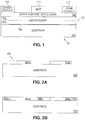
- FIGURE 1 illustrates a portion of an example semiconductor structure 100 having a multi-layer Group III-nitride buffer which was manufactured according to the claimed invention.
- the semiconductor structure 100 includes a substrate 102.
- the substrate 102 represents any suitable semiconductor substrate that supports or carries other components of the semiconductor structure 100.
- the substrate 102 could, for example, represent a silicon, sapphire, or silicon carbide substrate.
- the substrate 102 could represent a large-area substrate, such as a ⁇ 111> silicon wafer with a diameter of at least six inches.
- a nucleation layer 104 is formed over the substrate 102.
- the nucleation layer 104 could be formed from any suitable material(s), such as aluminum nitride.
- a buffer layer 106 is formed over the nucleation layer 104.
- the buffer layer 106 typically represents a layer used to help isolate other components in the semiconductor structure 100 from the substrate 102 and to provide a good starting surface (with minimized dislocations) for one or more Group III-nitride devices being formed.
- the buffer layer 106 could be formed from any suitable material(s), such as a Group III-nitride.
- a "Group III-nitride” refers to a compound formed using nitrogen and at least one Group III element.
- Example Group III elements include indium, gallium, and aluminum.
- Example Group III-nitrides include gallium nitride (GaN), aluminum gallium nitride (AlGaN), indium aluminum nitride (InAIN), indium aluminum gallium nitride (InAlGaN), aluminum nitride (AlN), indium nitride (InN), and indium gallium nitride (InGaN).
- the buffer layer 106 could be formed in any suitable manner, such as by using a metal-organic chemical vapor deposition (MOCVD) or Molecular Beam Epitaxy (MBE) technique. Note that the formation of the buffer layer 106 can be facilitated by the nucleation layer 104. However, the buffer layer 106 could be formed in a way that does not require the nucleation layer 104, and the layer 104 can be omitted.
- MOCVD metal-organic chemical vapor deposition
- MBE Molecular Beam Epitaxy
- At least one Group III-nitride device layer 108 is formed over the buffer layer 106.
- the Group III-nitride device layer 108 is used to form a portion of at least one semiconductor device, such as a gallium nitride-based field effect transistor (FET) or high electron mobility transistor (HEMT).
- the Group III-nitride device layer 108 could include any other or additional integrated circuit component(s).
- the Group III-nitride device layer 108 could be formed from any suitable Group III-nitride material(s).
- the Group III-nitride device layer 108 could also be formed in any suitable manner, such as during the same operation (like MOCVD or MBE) that is used to form the buffer layer 106.
- a "device layer” denotes all or a portion of a layer in which at least part of a semiconductor device is formed.
- a device layer could be formed as an individual layer or as part of another layer (such as an epitaxial layer).
- the formation of at least one Group III-nitride device could then be completed using the Group III-nitride device layer(s) 108.
- an upper portion of the buffer layer 106 or a portion of the device layer 108 could be doped with one or more dopants to create a source, a drain, or other transistor regions.
- One or more metal or other conductive layers could be patterned and etched to form source and drain contacts 110-112. Active regions in the structure could be isolated from one another, such as by mesa etching or ion-implantation.
- a gate 114 could be formed by etching, dielectric deposition, and deposition of metal or other conductive material. Connections to other devices or circuit elements could be made using the contacts 110-112 and the gate 114.
- the buffer layer 106 is fabricated as a multi-layer structure.
- a first portion 106a of the buffer layer 106 (such as a first Group III-nitride epitaxial layer) can be formed over the substrate 102.
- the first portion 106a of the buffer layer 106 can be processed, such as by etching the first portion 106a to form isolated epitaxial regions, which helps to relieve stress on the first portion 106a of the buffer layer 106.
- a second portion 106b of the buffer layer 106 (such as a second Group III-nitride epitaxial layer) is formed over the first portion 106a of the buffer layer 106, and the second portion 106b of the buffer layer 106 can be processed. If desired, one or more additional portions of the buffer layer 106 can be formed at this point.
- each epitaxial layer forming the buffer layer 106 could be between 1 ⁇ m and 3 ⁇ m in thickness (for six-inch and eight-inch diameter ⁇ 111> silicon substrates), providing a total thickness of up to 6 ⁇ m.
- each epitaxial layer forming the buffer layer 106 could have a thickness at or below its "cracking" thickness, which refers to the minimum thickness at which cracks appear in the epitaxial layer due to stresses from thermal expansion coefficient mismatches, wafer bowing, or lattice mismatch.
- the Group III-nitride device(s) formed using the device layer 108 would have a higher breakdown voltage compared to conventional Group III-nitride devices.
- larger silicon wafers or other substrates 102 could be used to fabricate multiple Group III-nitride devices, providing cost reduction per device fabricated.
- Various techniques for forming the multi-layer Group III-nitride buffer layer 106 are described below. Note that the different portions or layers in the buffer layer 106 could have the same thickness or different thicknesses, and the different portions or layers in the buffer layer 106 could be formed from the same material(s) or from different material(s).
- FIGURE 1 illustrates one example of a semiconductor structure 100 having a multi-layer Group III-nitride buffer
- any other materials and processes could be used to form various layers or other structures of the semiconductor structure 100.
- the sizes and shapes of the components in FIGURE 1 and the arrangements of those components in FIGURE 1 are for illustration only.
- FIGURES 2A through 2D illustrate a portion of a first example technique 200 for forming a semiconductor structure having a multi-layer Group III-nitride buffer according to the invention.
- a substrate 202 is fabricated or provided.
- the substrate 202 could represent any suitable semiconductor substrate, such as a silicon wafer having a diameter of six inches or more. Note that any other suitable substrate could be used, such as a silicon carbide or sapphire wafer or a smaller silicon wafer.
- Epitaxial regions 204a-204b are formed over the substrate 202.
- the epitaxial regions 204a-204b could be formed from any suitable material(s), such as one or more Group III-nitrides.
- the epitaxial regions 204a-204b could also have any suitable thickness, such as 1 ⁇ m-3 ⁇ m (which can typically be formed over larger substrates, like six-inch and eight-inch diameter ⁇ 111> silicon substrates, without cracking).
- the epitaxial regions 204a-204b could further be formed using any suitable technique(s), such as by using MOCVD, MBE, or other technique to form an epitaxial layer that is patterned and etched.
- the epitaxial layer could be formed using a nucleation layer (not shown) over the substrate 202.
- the epitaxial regions 204a-204b could represent areas of the epitaxial layer where semiconductor devices are to be formed.
- the removed portions of the epitaxial layer (around and between the epitaxial regions 204a-204b) could represent non-active areas of the epitaxial layer where no semiconductor devices are to be formed.
- dielectric regions 206a-206c are formed between and around the epitaxial regions 204a-204b.
- the dielectric regions 206a-206c help to electrically isolate the epitaxial regions 204a-204b
- the dielectric regions 206a-206c could be formed from any suitable material(s), such as silicon dioxide (SiO 2 ).
- the dielectric regions 206a-206c could be formed in any suitable manner, such as by forming a dielectric layer over and between the epitaxial regions 204a-204b and then performing a chemical mechanical polish (CMP) operation. This removes the dielectric layer above the epitaxial regions 204a-204b and planarizes the epitaxial regions 204a-204b and the dielectric regions 206a-206c.
- CMP chemical mechanical polish
- epitaxial regions 208a-208b are formed over the structure.
- the epitaxial regions 208a-208b could be formed from any suitable material(s), such as one or more Group III-nitrides.
- the epitaxial regions 208a-208b could also have any suitable thickness, such as 1 ⁇ m-3 ⁇ m.
- the epitaxial regions 208a-208b could further be formed using any suitable technique(s), such as selective deposition or growth using MOCVD or MBE.
- the selective deposition or growth means the epitaxial regions 208a-208b are generally formed over the exposed epitaxial regions 204a-204b, so the epitaxial regions 208a-208b are effectively self-aligned with the epitaxial regions 204a-204b.
- Some amorphous or other material can be deposited or grown on the dielectric regions 206a-206c during the selective operation, but this material can be removed or allowed to remain if it does not adversely affect operation of semiconductor devices being formed.
- dielectric regions 210a-210c are formed between and around the epitaxial regions 208a-208b, which helps to electrically isolate the epitaxial regions 208a-208b.
- the dielectric regions 210a-210c could be formed from any suitable material(s), such as SiO 2 .
- the dielectric regions 210a-210c could be formed in any suitable manner, such as by depositing a dielectric layer over and between the epitaxial regions 208a-208b and then performing a CMP operation. This removes the dielectric layer above the epitaxial regions 208a-208b and planarizes the epitaxial regions 208a-208b and the dielectric regions 210a-210c.
- the epitaxial regions 204a and 208a form a buffer layer 209a over which at least one transistor device or other integrated circuit device can be fabricated (assuming a device layer is formed over the region 208a).
- the epitaxial regions 204b and 208b form a buffer layer 209b over which at least one other transistor device or other integrated circuit device can be fabricated (assuming a device layer is formed over the region 208b).
- additional processing steps occur, such as the formation of Group III-nitride device layers and devices over the epitaxial regions 208a-208b. This is shown in FIGURES 3A and 3B .
- FIGURES 3A and 3B illustrate side and top views of the semiconductor structure formed in FIGURES 2A through 2D according to this disclosure.
- FIGURE 3A shows a side view 300 of the semiconductor structure
- FIGURE 3B shows a top view 350 of the semiconductor structure.
- inter-level dielectric (ILD) layer or other dielectric layer 302 is formed over the semiconductor structure of FIGURE 2D . This could occur after the Group III-nitride device layers and devices are formed over the semiconductor structure of FIGURE 2D .
- various structures 304 can be formed in the dielectric layer(s) 302.
- the dielectric layer 302 includes any suitable number of layers formed from any suitable dielectric material(s).
- the structures 304 could include any suitable structures for coupling to transistor devices or other devices, such as source, drain, and gate contacts, metal interconnects, and conductive plugs.
- conductive structures 306 can be formed over the dielectric layer 302 to provide electrical connection to external signal lines.
- the conductive structures 306 could be formed in any suitable manner using any suitable material(s), such as by depositing and etching a metal layer to form source and drain bond pads over each buffer 209a-209b. These components 304-306 could be fabricated in any suitable manner, such as by using conventional complimentary metal oxide semiconductor (CMOS) back-end manufacturing operations.
- CMOS complimentary metal oxide semiconductor
- a source contact 352 electrically contacts a source formed in the epitaxial region 208a.
- One or more conductive plugs 354 electrically couple the source contact 352 to a conductive interconnect 356, which is electrically coupled to another component (a source bond pad 306) by one or more conductive plugs 358.
- a drain contact 360 electrically contacts a drain formed on the epitaxial region 208a.
- One or more conductive plugs 362 electrically couple the drain contact 360 to a conductive interconnect 364, which is electrically coupled to another component (a drain bond pad 306) by one or more conductive plugs 366.
- a gate 368 is formed over the epitaxial region 208a. The gate 368 is in electrical contact with a gate bond pad 370.
- the bond pads could be electrically connected to other circuitry in a larger device.
- An isolation implant (such as one using nitrogen) can be performed outside of a region 372 of the structure to help avoid high voltages at the trench edges of the semiconductor device being formed in the epitaxial region 208a.
- Other techniques could be used to help isolate the semiconductor device being formed, such as by etching through the device layer and etching a portion of the buffer layer around the area where the semiconductor device is being formed.
- a source contact 374 electrically contacts a source formed on the epitaxial region 208b.
- One or more conductive plugs 376 electrically couple the source contact 374 to a conductive interconnect 378, which is electrically coupled to another component (a second source bond pad 306) by one or more conductive plugs 380.
- a drain contact 382 electrically contacts a drain formed on the epitaxial region 208b.
- One or more conductive plugs 384 electrically couple the drain contact 386 to a conductive interconnect 386, which is electrically coupled to another component (a second drain bond pad 306) by one or more conductive plugs 388.
- a gate 390 is formed over the epitaxial region 208b. The gate 390 is in electrical contact with a gate bond pad 392.
- the bond pads could be electrically connected to other circuitry in a larger device.
- An isolation implant can be performed outside of a region 394 of the structure to help avoid high voltages at the trench edges of the semiconductor device being formed in the epitaxial region 208b. Other isolation techniques could be used.
- Each of these components 352-394 could be formed from any suitable material(s) and using any suitable technique(s).
- transistor devices of differing sizes are formed using the buffers 209a-209b, although any number of devices could be fabricated in the same or similar manner and have any suitable size(s).
- the epitaxial regions 204a-204b and 208a-208b collectively form thicker buffers 209a-209b, such as buffers up to 6 ⁇ m or even more, without significant wafer bowing or cracking. Because the buffers 209a-209b are thicker, the transistor devices formed here could have significantly higher breakdown voltages. In addition, this could be achieved even using large semiconductor substrates, like six-inch or larger silicon wafers, which can provide significant cost savings.
- FIGURES 2A through 2D illustrate one example of a technique 200 for forming a semiconductor structure having a multi-layer Group III-nitride buffer and FIGURES 3A and 3B illustrate example views of the semiconductor structure
- various changes may be made to FIGURES 2A through 2D , 3A, and 3B .
- the relative sizes and shapes of the elements in the structure could be modified according to particular needs.
- additional components could be formed within the semiconductor structure, such as a nucleation layer or more than two epitaxial regions that are combined to form a single buffer.
- FIGURES 4A through 4C illustrate a second example technique 400 for forming a semiconductor structure having a multi-layer Group III-nitride buffer useful for understanding the invention.
- a substrate 402 is fabricated or provided. Any suitable semiconductor substrate could be used, such as a silicon wafer having a diameter of six inches or more.
- Epitaxial regions 404a-404b are formed over the substrate 402.
- the epitaxial regions 404a-404b could be formed from any suitable material(s), such as one or more Group III-nitrides.
- the epitaxial regions 404a-404b could also have any suitable thickness, such as 1 ⁇ m-3 ⁇ m.
- the epitaxial regions 404a-404b could further be formed using any suitable technique(s), such as by using MOCVD, MBE, or other technique to form an epitaxial layer that is patterned and etched.
- the epitaxial layer could be formed using a nucleation layer (not shown) formed over the substrate 402. Etching the epitaxial layer can help to relieve stress in the epitaxial layer 404.
- an epitaxial layer 406 is formed over the epitaxial regions 404a-404b and the substrate 402.
- the epitaxial layer 406 could be formed from any suitable material(s), such as one or more Group III-nitrides.
- the epitaxial layer 406 could also have any suitable thickness, such as 1 ⁇ m-3 ⁇ m.
- the epitaxial layer 406 could further be formed using any suitable technique(s), such as MOCVD or MBE.
- the epitaxial layer 406 could be etched to isolate epitaxial regions 406a-406b of the epitaxial layer 406 as shown in FIGURE 4C .
- the etching can also help to relieve stress in the epitaxial layer 406.
- the epitaxial regions 404a-404b and the epitaxial regions 406a-406b can form buffers 407a-407b.
- Transistor devices or other integrated circuit components can be formed in or over the buffers 407a-407b (assuming device layers are formed as part of or over the epitaxial regions 406a-406b).
- the combined thickness of the epitaxial regions 404a-404b and epitaxial regions 406a-406b can provide higher breakdown voltages for those devices because the combined thickness exceeds the maximum thickness possible by only a single growth.
- the epitaxial layer 406 is not grown very thick (such as 1 ⁇ m to 3 ⁇ m), it can be left unetched in order to reduce processing costs.
- FIGURES 5A through 5C illustrate a third example technique 500 for forming a semiconductor structure having a multi-layer Group III-nitride buffer according to this disclosure, which does not form part of the claimed invention.
- a semiconductor substrate 502 is fabricated or provided.
- Epitaxial regions 504a-504d are formed over the substrate 502.
- the epitaxial regions 504a-504d could be formed from any suitable material(s) and in any suitable manner.
- the epitaxial regions 504a-504d could be formed by etching a Group III-nitride epitaxial layer.
- the etching can form trenches 506 between the epitaxial regions 504a-504d, which can help to relieve stress on the epitaxial regions 504a-504d.
- the etching could occur as shown in FIGURE 5B , which shows the trenches 506 forming a grid pattern 508.
- an epitaxial layer 510 is formed in the trenches 506 and over the epitaxial regions 504a-504d and the substrate 502.
- the epitaxial layer 510 could be formed from any suitable material(s) and in any suitable manner. While not shown, the epitaxial layer 510 could be etched to isolate different regions of the epitaxial layer 510. The etching can also help to relieve stress on the epitaxial layer 510. Regardless of whether the epitaxial layer 510 is etched, transistor devices or other integrated circuit components can be formed in or over regions of the epitaxial layer 510 (assuming a device layer is formed as part of or over the epitaxial layer 510).
- the combined thickness of the epitaxial regions 502a-502d and the epitaxial layer 510 can provide higher breakdown voltages for those devices because the combined thickness exceeds the maximum thickness possible by only a single growth.
- FIGURES 4A through 5C illustrate two additional examples of techniques for forming a semiconductor structure having a multi-layer Group III-nitride buffer
- each element in the structures could be fabricated using any suitable material(s) and any suitable technique(s).
- the relative sizes and shapes of the elements in the structures could be modified according to particular needs.
- additional components could be formed within the semiconductor structures, such as nucleation layers or more than two epitaxial regions that are combined to form a single buffer.
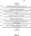
- FIGURE 6 illustrates an example method 600 for forming a semiconductor structure having a multi-layer Group III-nitride buffer according to the claimed invention.
- the method 600 is described with respect to the technique shown in FIGURES 2A through 2D .
- a first portion of a buffer is formed over a substrate at step 602, and the first portion of the buffer is processed at step 604.
- This could include, for example, forming the epitaxial regions 204a-204b over the substrate 202.
- this could include forming an epitaxial layer over the substrate 202, patterning a mask over what is to become epitaxial regions 204a and 204b, and etching the epitaxial layer in areas not protected by the mask to form the epitaxial regions 204a-204b.
- This could also include forming isolating dielectric regions 206a-206c around the epitaxial regions 204a-204b.
- first portion of the buffer a single epitaxial layer or multiple epitaxial layers could be used to form the first portion of the buffer.
- the layers may be identical or different, and each layer could be uniform or graded.
- Another technique for forming the first portion of the buffer with isolated regions is disclosed in U.S. Patent Application No. 12/577576 .
- a second portion of the buffer is formed over the first portion of the buffer at step 606, and the second portion of the buffer is processed at step 608.
- This could include, for example, forming the epitaxial regions 208a-208b over the epitaxial regions 204a-204b.
- this could include forming an epitaxial layer over the epitaxial regions 204a-204b, patterning a mask over what is to become epitaxial regions 208a and 208b, and etching the unmasked epitaxial layer to form the epitaxial regions 208a-208b.
- this could include selectively forming the epitaxial regions 208a-208b over the epitaxial regions 204a-204b.
- One or more Group III-nitride devices are formed over the buffer at step 610. This includes, for example, forming sources, drains, and other device structures in a device layer 108 formed over the epitaxial regions 208a-208b. Contacts and one or more dielectric layers are formed over the Group III-nitride device(s) at step 614. This could include, for example, forming source, drain, and gate contacts over the Group III-nitride device(s). This could also include forming an ILD layer or other dielectric layer 302 over the Group III-nitride device(s) and over the source, drain, and gate contacts. Interconnect structures are formed over the Group III-nitride device(s) at step 616. This could include, for example, forming conductive interconnects and conductive plugs to couple the source, drain, and gate contacts to bond pads or other structures.
- FIGURE 6 illustrates one example of a method 600 for forming a semiconductor structure having a multi-layer Group III-nitride buffer
- various changes may be made to FIGURE 6 .
- steps in FIGURE 6 could overlap, occur in parallel, occur in a different order, or occur multiple times.
- Couple and its derivatives refer to any direct or indirect communication between two or more components, whether or not those components are in physical contact with one another.
- the term “or” is inclusive, meaning and/or.
- phrases "associated with” and “associated therewith,” as well as derivatives thereof, may mean to include, be included within, interconnect with, contain, be contained within, connect to or with, couple to or with, be communicable with, cooperate with, interleave, juxtapose, be proximate to, be bound to or with, have, have a property of, have a relationship to or with, or the like.
Description
- This disclosure is generally directed to integrated circuits. More specifically, this disclosure is directed to the growth of multi-layer Group III-nitride buffers on large-area silicon substrates and other substrates.
- Gallium nitride (GaN) and other "Group III-nitrides" can be used in manufacturing high-speed or high-power integrated circuit devices. Gallium nitride is often desirable because it can withstand high operating temperatures and can provide high breakdown voltages compared to standard silicon devices. Gallium nitride can also typically provide good high-frequency performance and provide lower on resistances.
- Native gallium nitride substrates are not generally available. Instead, gallium nitride epitaxial layers are often formed over silicon-based substrates, such as <111> silicon wafers. However, it is often difficult to form thick high-quality gallium nitride epitaxial layers over large silicon substrates. This is due to a number of factors, including large thermal expansion coefficient mismatches and wafer bowing. More specifically, a gallium nitride epitaxial layer can contract about twice as fast when cooled compared to an underlying silicon substrate. This causes tensile stress in the gallium nitride epitaxial layer, which can lead to wafer bowing and produce cracks in the epitaxial layer. These problems are worse with larger substrates, such as silicon wafers with six-inch or larger diameters.
- The inability to form thick high-quality gallium nitride layers can reduce the breakdown voltage of field effect transistors (FETs), high electron mobility transistors (HEMTs), or other devices formed using the gallium nitride layers. Also, the production of circuits on larger substrates is typically desired since the same processing steps can be used to fabricate a larger number of circuits on the substrates, resulting in a production cost reduction per circuit. The inability to form thick high-quality gallium nitride layers over larger substrates can limit or eliminate these cost reductions, resulting in higher-cost circuits. In addition, wafer bowing and epitaxial layer cracking can actually limit the manufacturability of certain gallium nitride-based circuits.
- A method for forming substantially continuous layers of group III nitride semiconductor material with low defect densities is disclosed in International Publication
WO 2009/015350A1 . Islands of gallium nitride are formed on a semiconductor substrate in two consecutive steps, and voids are provided between neighboring islands to serve as localized weakened zones within the structure so that the structure may be separated by applying an external force. - A group III nitride semiconductor structure and fabrication method in which isolated buffer layers are separated by mask material on a semiconductor substrate is disclosed in
EP 1280190A1 . - United States Patent Application
US 2005/0124143A1 discloses a method in which small defects in a gallium nitride layer are widened to form enlarged cavities, which are then subsequently filled with another epitaxial layer of gallium nitride. - A semiconductor structure in which a plurality of stacked layers, comprising a buffer layer, are formed on a semiconductor substrate and are interspersed by insulating layers is disclosed in United States Patent Application
US 2003/008746A1 . - The present invention provides a method according to claim 1. Preferred embodiments of the invention are defined in dependent claims.
- For a more complete understanding of this disclosure and its features, reference is now made to the following description, taken in conjunction with the accompanying drawings, in which:
-
FIGURE 1 illustrates a portion of an example semiconductor structure having a multi-layer Group III-nitride buffer which was manufactured according to the invention; -
FIGURES 2A through 2D illustrate a portion of a first example technique for forming a semiconductor structure having a multi-layer Group III-nitride buffer according to the claimed invention; -
FIGURES 3A and 3B illustrate side and top views of the semiconductor structure formed inFIGURES 2A through 2D according to the claimed invention; -
FIGURES 4A through 4C illustrate a second example technique for forming a semiconductor structure having a multi-layer Group III-nitride buffer useful for understanding the invention; -
FIGURES 5A through 5C illustrate a third example technique for forming a semiconductor structure having a multi-layer Group III-nitride buffer useful for understanding the invention; and -
FIGURE 6 illustrates an example method for forming a semiconductor structure having a multi-layer Group III-nitride buffer according to the claimed invention. -
FIGURES 1 through 6 , discussed below, and the various embodiments describe the principles of the present invention. -
FIGURE 1 illustrates a portion of anexample semiconductor structure 100 having a multi-layer Group III-nitride buffer which was manufactured according to the claimed invention. As shown inFIGURE 1 , thesemiconductor structure 100 includes asubstrate 102. Thesubstrate 102 represents any suitable semiconductor substrate that supports or carries other components of thesemiconductor structure 100. Thesubstrate 102 could, for example, represent a silicon, sapphire, or silicon carbide substrate. In particular embodiments, thesubstrate 102 could represent a large-area substrate, such as a <111> silicon wafer with a diameter of at least six inches. Anucleation layer 104 is formed over thesubstrate 102. Thenucleation layer 104 could be formed from any suitable material(s), such as aluminum nitride. - A
buffer layer 106 is formed over thenucleation layer 104. Thebuffer layer 106 typically represents a layer used to help isolate other components in thesemiconductor structure 100 from thesubstrate 102 and to provide a good starting surface (with minimized dislocations) for one or more Group III-nitride devices being formed. Thebuffer layer 106 could be formed from any suitable material(s), such as a Group III-nitride. A "Group III-nitride" refers to a compound formed using nitrogen and at least one Group III element. Example Group III elements include indium, gallium, and aluminum. Example Group III-nitrides include gallium nitride (GaN), aluminum gallium nitride (AlGaN), indium aluminum nitride (InAIN), indium aluminum gallium nitride (InAlGaN), aluminum nitride (AlN), indium nitride (InN), and indium gallium nitride (InGaN). Thebuffer layer 106 could be formed in any suitable manner, such as by using a metal-organic chemical vapor deposition (MOCVD) or Molecular Beam Epitaxy (MBE) technique. Note that the formation of thebuffer layer 106 can be facilitated by thenucleation layer 104. However, thebuffer layer 106 could be formed in a way that does not require thenucleation layer 104, and thelayer 104 can be omitted. - At least one Group III-
nitride device layer 108 is formed over thebuffer layer 106. The Group III-nitride device layer 108 is used to form a portion of at least one semiconductor device, such as a gallium nitride-based field effect transistor (FET) or high electron mobility transistor (HEMT). The Group III-nitride device layer 108 could include any other or additional integrated circuit component(s). The Group III-nitride device layer 108 could be formed from any suitable Group III-nitride material(s). The Group III-nitride device layer 108 could also be formed in any suitable manner, such as during the same operation (like MOCVD or MBE) that is used to form thebuffer layer 106. In general, a "device layer" denotes all or a portion of a layer in which at least part of a semiconductor device is formed. A device layer could be formed as an individual layer or as part of another layer (such as an epitaxial layer). - The formation of at least one Group III-nitride device could then be completed using the Group III-nitride device layer(s) 108. For example, an upper portion of the
buffer layer 106 or a portion of thedevice layer 108 could be doped with one or more dopants to create a source, a drain, or other transistor regions. One or more metal or other conductive layers could be patterned and etched to form source and drain contacts 110-112. Active regions in the structure could be isolated from one another, such as by mesa etching or ion-implantation. Agate 114 could be formed by etching, dielectric deposition, and deposition of metal or other conductive material. Connections to other devices or circuit elements could be made using the contacts 110-112 and thegate 114. - In order to help increase the thickness of the
buffer layer 106, thebuffer layer 106 is fabricated as a multi-layer structure. Afirst portion 106a of the buffer layer 106 (such as a first Group III-nitride epitaxial layer) can be formed over thesubstrate 102. Thefirst portion 106a of thebuffer layer 106 can be processed, such as by etching thefirst portion 106a to form isolated epitaxial regions, which helps to relieve stress on thefirst portion 106a of thebuffer layer 106. Asecond portion 106b of the buffer layer 106 (such as a second Group III-nitride epitaxial layer) is formed over thefirst portion 106a of thebuffer layer 106, and thesecond portion 106b of thebuffer layer 106 can be processed. If desired, one or more additional portions of thebuffer layer 106 can be formed at this point. - These different portions could collectively form a
buffer layer 106 that is thicker than those obtained using the conventional techniques described above. For example, each epitaxial layer forming thebuffer layer 106 could be between 1µm and 3µm in thickness (for six-inch and eight-inch diameter <111> silicon substrates), providing a total thickness of up to 6µm. In general, each epitaxial layer forming thebuffer layer 106 could have a thickness at or below its "cracking" thickness, which refers to the minimum thickness at which cracks appear in the epitaxial layer due to stresses from thermal expansion coefficient mismatches, wafer bowing, or lattice mismatch. As a result of thethicker buffer layer 106, the Group III-nitride device(s) formed using thedevice layer 108 would have a higher breakdown voltage compared to conventional Group III-nitride devices. Moreover, larger silicon wafers orother substrates 102 could be used to fabricate multiple Group III-nitride devices, providing cost reduction per device fabricated. Various techniques for forming the multi-layer Group III-nitride buffer layer 106 are described below. Note that the different portions or layers in thebuffer layer 106 could have the same thickness or different thicknesses, and the different portions or layers in thebuffer layer 106 could be formed from the same material(s) or from different material(s). - Although
FIGURE 1 illustrates one example of asemiconductor structure 100 having a multi-layer Group III-nitride buffer, various changes may be made toFIGURE 1 . For example, any other materials and processes could be used to form various layers or other structures of thesemiconductor structure 100. Also, the sizes and shapes of the components inFIGURE 1 and the arrangements of those components inFIGURE 1 are for illustration only. -
FIGURES 2A through 2D illustrate a portion of afirst example technique 200 for forming a semiconductor structure having a multi-layer Group III-nitride buffer according to the invention. As shown inFIGURE 2A , asubstrate 202 is fabricated or provided. Thesubstrate 202 could represent any suitable semiconductor substrate, such as a silicon wafer having a diameter of six inches or more. Note that any other suitable substrate could be used, such as a silicon carbide or sapphire wafer or a smaller silicon wafer. -
Epitaxial regions 204a-204b are formed over thesubstrate 202. Theepitaxial regions 204a-204b could be formed from any suitable material(s), such as one or more Group III-nitrides. Theepitaxial regions 204a-204b could also have any suitable thickness, such as 1µm-3µm (which can typically be formed over larger substrates, like six-inch and eight-inch diameter <111> silicon substrates, without cracking). Theepitaxial regions 204a-204b could further be formed using any suitable technique(s), such as by using MOCVD, MBE, or other technique to form an epitaxial layer that is patterned and etched. The epitaxial layer could be formed using a nucleation layer (not shown) over thesubstrate 202. Theepitaxial regions 204a-204b could represent areas of the epitaxial layer where semiconductor devices are to be formed. The removed portions of the epitaxial layer (around and between theepitaxial regions 204a-204b) could represent non-active areas of the epitaxial layer where no semiconductor devices are to be formed. - As shown in
FIGURE 2B ,dielectric regions 206a-206c are formed between and around theepitaxial regions 204a-204b. Thedielectric regions 206a-206c help to electrically isolate theepitaxial regions 204a-204b, Thedielectric regions 206a-206c could be formed from any suitable material(s), such as silicon dioxide (SiO2). Also, thedielectric regions 206a-206c could be formed in any suitable manner, such as by forming a dielectric layer over and between theepitaxial regions 204a-204b and then performing a chemical mechanical polish (CMP) operation. This removes the dielectric layer above theepitaxial regions 204a-204b and planarizes theepitaxial regions 204a-204b and thedielectric regions 206a-206c. - As shown in
FIGURE 2C ,epitaxial regions 208a-208b are formed over the structure. Theepitaxial regions 208a-208b could be formed from any suitable material(s), such as one or more Group III-nitrides. Theepitaxial regions 208a-208b could also have any suitable thickness, such as 1µm-3µm. Theepitaxial regions 208a-208b could further be formed using any suitable technique(s), such as selective deposition or growth using MOCVD or MBE. The selective deposition or growth means theepitaxial regions 208a-208b are generally formed over the exposedepitaxial regions 204a-204b, so theepitaxial regions 208a-208b are effectively self-aligned with theepitaxial regions 204a-204b. Some amorphous or other material can be deposited or grown on thedielectric regions 206a-206c during the selective operation, but this material can be removed or allowed to remain if it does not adversely affect operation of semiconductor devices being formed. - As shown in
FIGURE 2D ,dielectric regions 210a-210c are formed between and around theepitaxial regions 208a-208b, which helps to electrically isolate theepitaxial regions 208a-208b. Thedielectric regions 210a-210c could be formed from any suitable material(s), such as SiO2. Also, thedielectric regions 210a-210c could be formed in any suitable manner, such as by depositing a dielectric layer over and between theepitaxial regions 208a-208b and then performing a CMP operation. This removes the dielectric layer above theepitaxial regions 208a-208b and planarizes theepitaxial regions 208a-208b and thedielectric regions 210a-210c. - The
epitaxial regions buffer layer 209a over which at least one transistor device or other integrated circuit device can be fabricated (assuming a device layer is formed over theregion 208a). Similarly, theepitaxial regions buffer layer 209b over which at least one other transistor device or other integrated circuit device can be fabricated (assuming a device layer is formed over theregion 208b). At this point, additional processing steps occur, such as the formation of Group III-nitride device layers and devices over theepitaxial regions 208a-208b. This is shown inFIGURES 3A and 3B . -
FIGURES 3A and 3B illustrate side and top views of the semiconductor structure formed inFIGURES 2A through 2D according to this disclosure. In particular,FIGURE 3A shows aside view 300 of the semiconductor structure, whileFIGURE 3B shows atop view 350 of the semiconductor structure. - As shown in
FIGURE 3A , at least one inter-level dielectric (ILD) layer or otherdielectric layer 302 is formed over the semiconductor structure ofFIGURE 2D . This could occur after the Group III-nitride device layers and devices are formed over the semiconductor structure ofFIGURE 2D . Also,various structures 304 can be formed in the dielectric layer(s) 302. Thedielectric layer 302 includes any suitable number of layers formed from any suitable dielectric material(s). Thestructures 304 could include any suitable structures for coupling to transistor devices or other devices, such as source, drain, and gate contacts, metal interconnects, and conductive plugs. In addition,conductive structures 306 can be formed over thedielectric layer 302 to provide electrical connection to external signal lines. Theconductive structures 306 could be formed in any suitable manner using any suitable material(s), such as by depositing and etching a metal layer to form source and drain bond pads over eachbuffer 209a-209b. These components 304-306 could be fabricated in any suitable manner, such as by using conventional complimentary metal oxide semiconductor (CMOS) back-end manufacturing operations. - In
FIGURE 3B , asource contact 352 electrically contacts a source formed in theepitaxial region 208a. One or moreconductive plugs 354 electrically couple thesource contact 352 to aconductive interconnect 356, which is electrically coupled to another component (a source bond pad 306) by one or moreconductive plugs 358. Similarly, adrain contact 360 electrically contacts a drain formed on theepitaxial region 208a. One or moreconductive plugs 362 electrically couple thedrain contact 360 to aconductive interconnect 364, which is electrically coupled to another component (a drain bond pad 306) by one or moreconductive plugs 366. Agate 368 is formed over theepitaxial region 208a. Thegate 368 is in electrical contact with agate bond pad 370. The bond pads could be electrically connected to other circuitry in a larger device. An isolation implant (such as one using nitrogen) can be performed outside of aregion 372 of the structure to help avoid high voltages at the trench edges of the semiconductor device being formed in theepitaxial region 208a. Other techniques could be used to help isolate the semiconductor device being formed, such as by etching through the device layer and etching a portion of the buffer layer around the area where the semiconductor device is being formed. - In a similar manner, a
source contact 374 electrically contacts a source formed on theepitaxial region 208b. One or moreconductive plugs 376 electrically couple thesource contact 374 to aconductive interconnect 378, which is electrically coupled to another component (a second source bond pad 306) by one or moreconductive plugs 380. Adrain contact 382 electrically contacts a drain formed on theepitaxial region 208b. One or moreconductive plugs 384 electrically couple thedrain contact 386 to aconductive interconnect 386, which is electrically coupled to another component (a second drain bond pad 306) by one or moreconductive plugs 388. Agate 390 is formed over theepitaxial region 208b. Thegate 390 is in electrical contact with agate bond pad 392. The bond pads could be electrically connected to other circuitry in a larger device. An isolation implant can be performed outside of aregion 394 of the structure to help avoid high voltages at the trench edges of the semiconductor device being formed in theepitaxial region 208b. Other isolation techniques could be used. - Each of these components 352-394 could be formed from any suitable material(s) and using any suitable technique(s). In this example, transistor devices of differing sizes are formed using the
buffers 209a-209b, although any number of devices could be fabricated in the same or similar manner and have any suitable size(s). Moreover, theepitaxial regions 204a-204b and 208a-208b collectively formthicker buffers 209a-209b, such as buffers up to 6µm or even more, without significant wafer bowing or cracking. Because thebuffers 209a-209b are thicker, the transistor devices formed here could have significantly higher breakdown voltages. In addition, this could be achieved even using large semiconductor substrates, like six-inch or larger silicon wafers, which can provide significant cost savings. - Although
FIGURES 2A through 2D illustrate one example of atechnique 200 for forming a semiconductor structure having a multi-layer Group III-nitride buffer andFIGURES 3A and 3B illustrate example views of the semiconductor structure, various changes may be made toFIGURES 2A through 2D ,3A, and 3B . The relative sizes and shapes of the elements in the structure could be modified according to particular needs. In addition, additional components could be formed within the semiconductor structure, such as a nucleation layer or more than two epitaxial regions that are combined to form a single buffer. -
FIGURES 4A through 4C illustrate asecond example technique 400 for forming a semiconductor structure having a multi-layer Group III-nitride buffer useful for understanding the invention. As shown inFIGURE 4A , asubstrate 402 is fabricated or provided. Any suitable semiconductor substrate could be used, such as a silicon wafer having a diameter of six inches or more.Epitaxial regions 404a-404b are formed over thesubstrate 402. Theepitaxial regions 404a-404b could be formed from any suitable material(s), such as one or more Group III-nitrides. Theepitaxial regions 404a-404b could also have any suitable thickness, such as 1µm-3µm. Theepitaxial regions 404a-404b could further be formed using any suitable technique(s), such as by using MOCVD, MBE, or other technique to form an epitaxial layer that is patterned and etched. The epitaxial layer could be formed using a nucleation layer (not shown) formed over thesubstrate 402. Etching the epitaxial layer can help to relieve stress in the epitaxial layer 404. - As shown in
FIGURE 4B , anepitaxial layer 406 is formed over theepitaxial regions 404a-404b and thesubstrate 402. Theepitaxial layer 406 could be formed from any suitable material(s), such as one or more Group III-nitrides. Theepitaxial layer 406 could also have any suitable thickness, such as 1µm-3µm. Theepitaxial layer 406 could further be formed using any suitable technique(s), such as MOCVD or MBE. - The
epitaxial layer 406 could be etched to isolateepitaxial regions 406a-406b of theepitaxial layer 406 as shown inFIGURE 4C . The etching can also help to relieve stress in theepitaxial layer 406. Theepitaxial regions 404a-404b and theepitaxial regions 406a-406b can formbuffers 407a-407b. Transistor devices or other integrated circuit components can be formed in or over thebuffers 407a-407b (assuming device layers are formed as part of or over theepitaxial regions 406a-406b). The combined thickness of theepitaxial regions 404a-404b andepitaxial regions 406a-406b can provide higher breakdown voltages for those devices because the combined thickness exceeds the maximum thickness possible by only a single growth. Alternatively, if theepitaxial layer 406 is not grown very thick (such as 1µm to 3µm), it can be left unetched in order to reduce processing costs. -
FIGURES 5A through 5C illustrate athird example technique 500 for forming a semiconductor structure having a multi-layer Group III-nitride buffer according to this disclosure, which does not form part of the claimed invention. As shown inFIGURE 5A , asemiconductor substrate 502 is fabricated or provided.Epitaxial regions 504a-504d are formed over thesubstrate 502. Theepitaxial regions 504a-504d could be formed from any suitable material(s) and in any suitable manner. For instance, theepitaxial regions 504a-504d could be formed by etching a Group III-nitride epitaxial layer. The etching can formtrenches 506 between theepitaxial regions 504a-504d, which can help to relieve stress on theepitaxial regions 504a-504d. The etching could occur as shown inFIGURE 5B , which shows thetrenches 506 forming agrid pattern 508. - As shown in
FIGURE 5C , anepitaxial layer 510 is formed in thetrenches 506 and over theepitaxial regions 504a-504d and thesubstrate 502. Theepitaxial layer 510 could be formed from any suitable material(s) and in any suitable manner. While not shown, theepitaxial layer 510 could be etched to isolate different regions of theepitaxial layer 510. The etching can also help to relieve stress on theepitaxial layer 510. Regardless of whether theepitaxial layer 510 is etched, transistor devices or other integrated circuit components can be formed in or over regions of the epitaxial layer 510 (assuming a device layer is formed as part of or over the epitaxial layer 510). The combined thickness of the epitaxial regions 502a-502d and theepitaxial layer 510 can provide higher breakdown voltages for those devices because the combined thickness exceeds the maximum thickness possible by only a single growth. - Although
FIGURES 4A through 5C illustrate two additional examples of techniques for forming a semiconductor structure having a multi-layer Group III-nitride buffer, various changes may be made toFIGURES 4A through 5C . For example, each element in the structures could be fabricated using any suitable material(s) and any suitable technique(s). Also, the relative sizes and shapes of the elements in the structures could be modified according to particular needs. In addition, additional components could be formed within the semiconductor structures, such as nucleation layers or more than two epitaxial regions that are combined to form a single buffer. -
FIGURE 6 illustrates anexample method 600 for forming a semiconductor structure having a multi-layer Group III-nitride buffer according to the claimed invention. For ease of explanation, themethod 600 is described with respect to the technique shown inFIGURES 2A through 2D . - As shown in
FIGURE 6 , a first portion of a buffer is formed over a substrate atstep 602, and the first portion of the buffer is processed atstep 604. This could include, for example, forming theepitaxial regions 204a-204b over thesubstrate 202. As a particular example, this could include forming an epitaxial layer over thesubstrate 202, patterning a mask over what is to becomeepitaxial regions epitaxial regions 204a-204b. This could also include forming isolatingdielectric regions 206a-206c around theepitaxial regions 204a-204b. Note that a single epitaxial layer or multiple epitaxial layers could be used to form the first portion of the buffer. The layers may be identical or different, and each layer could be uniform or graded. Another technique for forming the first portion of the buffer with isolated regions is disclosed inU.S. Patent Application No. 12/577576 . - A second portion of the buffer is formed over the first portion of the buffer at
step 606, and the second portion of the buffer is processed atstep 608. This could include, for example, forming theepitaxial regions 208a-208b over theepitaxial regions 204a-204b. As a particular example, this could include forming an epitaxial layer over theepitaxial regions 204a-204b, patterning a mask over what is to becomeepitaxial regions epitaxial regions 208a-208b. As another particular example, this could include selectively forming theepitaxial regions 208a-208b over theepitaxial regions 204a-204b. This could also include forming isolatingdielectric regions 210a-210c around theepitaxial regions 208a-208b. Theepitaxial regions 204a-204b and 208a-208b collectively form thicker buffers that may not suffer from significant cracking or cause significant wafer bowing. Note that a single epitaxial layer or multiple epitaxial layers could be used to form the second portion of the buffer. The layers may be identical or different, and each layer could be uniform or graded. - One or more Group III-nitride devices are formed over the buffer at
step 610. This includes, for example, forming sources, drains, and other device structures in adevice layer 108 formed over theepitaxial regions 208a-208b. Contacts and one or more dielectric layers are formed over the Group III-nitride device(s) atstep 614. This could include, for example, forming source, drain, and gate contacts over the Group III-nitride device(s). This could also include forming an ILD layer or otherdielectric layer 302 over the Group III-nitride device(s) and over the source, drain, and gate contacts. Interconnect structures are formed over the Group III-nitride device(s) atstep 616. This could include, for example, forming conductive interconnects and conductive plugs to couple the source, drain, and gate contacts to bond pads or other structures. - Although
FIGURE 6 illustrates one example of amethod 600 for forming a semiconductor structure having a multi-layer Group III-nitride buffer, various changes may be made toFIGURE 6 . For example, while shown as a series of steps, various steps inFIGURE 6 could overlap, occur in parallel, occur in a different order, or occur multiple times. - It may be advantageous to set forth definitions of certain words and phrases that have been used within this patent document. The term "couple" and its derivatives refer to any direct or indirect communication between two or more components, whether or not those components are in physical contact with one another. The terms "include" and "comprise," as well as derivatives thereof, mean inclusion without limitation. The term "or" is inclusive, meaning and/or. The phrases "associated with" and "associated therewith," as well as derivatives thereof, may mean to include, be included within, interconnect with, contain, be contained within, connect to or with, couple to or with, be communicable with, cooperate with, interleave, juxtapose, be proximate to, be bound to or with, have, have a property of, have a relationship to or with, or the like.
Claims (2)
- A method comprising:forming a first epitaxial layer over a substrate (102; 202);etching the first epitaxial layer to form multiple separated first epitaxial regions (106a; 204a, 204b);depositing a first dielectric material (206a, 206b, 206c) around the first epitaxial regions (106a; 204a, 204b) and planarizing the first dielectric material (206a, 206b, 206c) and the first epitaxial regions (106a; 204a, 204b);selectively forming second epitaxial regions (106b; 208a, 208b) substantially only on the first epitaxial regions (106a; 204a, 204b) to provide a second epitaxial layer over the etched first epitaxial layer; depositing a second dielectric material (210a, 210b, 210c) around the second epitaxial regions (106b; 208a, 208b) and planarizing the second dielectric material and the second epitaxial regions,each of the epitaxial layers comprising at least one Group III-nitride, the epitaxial layers collectively forming a buffer (106); andforming a device layer (108); in which at least part of a semiconductor device is formable,wherein the device layer is formed as an individual layer (108) over the buffer (106).
- The method of Claim 1, wherein forming the second epitaxial layer comprises covering the first epitaxial regions (106a; 204a, 204b) and the substrate (102; 202) with the second epitaxial layer, and etching the second epitaxial layer to form multiple separated second epitaxial regions (106b; 208a, 208b).
Applications Claiming Priority (1)
| Application Number | Priority Date | Filing Date | Title |
|---|---|---|---|
| US12/807,336 US8592292B2 (en) | 2010-09-02 | 2010-09-02 | Growth of multi-layer group III-nitride buffers on large-area silicon substrates and other substrates |
Publications (2)
| Publication Number | Publication Date |
|---|---|
| EP2426699A1 EP2426699A1 (en) | 2012-03-07 |
| EP2426699B1 true EP2426699B1 (en) | 2019-02-27 |
Family
ID=44582433
Family Applications (1)
| Application Number | Title | Priority Date | Filing Date |
|---|---|---|---|
| EP11178555.6A Active EP2426699B1 (en) | 2010-09-02 | 2011-08-24 | Growth of multi-layer group III-nitride buffers on large-area silicon substrates and other substrates |
Country Status (3)
| Country | Link |
|---|---|
| US (3) | US8592292B2 (en) |
| EP (1) | EP2426699B1 (en) |
| JP (1) | JP5907686B2 (en) |
Families Citing this family (12)
| Publication number | Priority date | Publication date | Assignee | Title |
|---|---|---|---|---|
| US2985434A (en) * | 1957-03-15 | 1961-05-23 | Air Preheater | Regenerator |
| JP2012084743A (en) | 2010-10-13 | 2012-04-26 | Fujitsu Semiconductor Ltd | Semiconductor device and power supply device |
| US9129827B2 (en) | 2012-04-13 | 2015-09-08 | Intel Corporation | Conversion of strain-inducing buffer to electrical insulator |
| CN104641453B (en) * | 2012-10-12 | 2018-03-30 | 住友电气工业株式会社 | Group III nitride composite substrate and its manufacture method and the method for manufacturing Group III nitride semiconductor device |
| DE112013007031B4 (en) * | 2013-06-28 | 2022-02-24 | Intel Corporation | Devices based on selectively epitaxially grown III-V materials |
| US9978844B2 (en) | 2013-08-01 | 2018-05-22 | Taiwan Semiconductor Manufacturing Co., Ltd. | HEMT-compatible lateral rectifier structure |
| CN105409005B (en) | 2013-08-23 | 2019-04-02 | 英特尔公司 | The resistive formation of the III-V channel deposited on the IV race substrate of MOS transistor |
| US10032911B2 (en) | 2013-12-23 | 2018-07-24 | Intel Corporation | Wide band gap transistor on non-native semiconductor substrate |
| EP3087612A4 (en) * | 2013-12-23 | 2017-07-26 | Intel Corporation | Wide band gap transistors on non-native semiconductor substrates and methods of manufacture thereof |
| DE102014107560A1 (en) | 2014-05-28 | 2015-12-03 | Infineon Technologies Austria Ag | Semiconductor device and method |
| US20150372096A1 (en) * | 2014-06-20 | 2015-12-24 | Ishiang Shih | High Electron Mobility Transistors and Integrated Circuits with Improved Feature Uniformity and Reduced defects for Microwave and Millimetre Wave Applications |
| US11158575B2 (en) * | 2018-06-05 | 2021-10-26 | Macom Technology Solutions Holdings, Inc. | Parasitic capacitance reduction in GaN-on-silicon devices |
Family Cites Families (33)
| Publication number | Priority date | Publication date | Assignee | Title |
|---|---|---|---|---|
| JP3352712B2 (en) | 1991-12-18 | 2002-12-03 | 浩 天野 | Gallium nitride based semiconductor device and method of manufacturing the same |
| JPH08316152A (en) | 1995-05-23 | 1996-11-29 | Matsushita Electric Works Ltd | Crystal growing method for compound semiconductor |
| JP3257442B2 (en) | 1997-04-09 | 2002-02-18 | 松下電器産業株式会社 | Method for producing gallium nitride crystal |
| TW428331B (en) * | 1998-05-28 | 2001-04-01 | Sumitomo Electric Industries | Gallium nitride single crystal substrate and method of producing the same |
| JP2000012467A (en) | 1998-06-24 | 2000-01-14 | Oki Electric Ind Co Ltd | Method for forming gaas layer |
| JP3702700B2 (en) * | 1999-03-31 | 2005-10-05 | 豊田合成株式会社 | Group III nitride compound semiconductor device and method for manufacturing the same |
| US6521514B1 (en) * | 1999-11-17 | 2003-02-18 | North Carolina State University | Pendeoepitaxial methods of fabricating gallium nitride semiconductor layers on sapphire substrates |
| US6261929B1 (en) * | 2000-02-24 | 2001-07-17 | North Carolina State University | Methods of forming a plurality of semiconductor layers using spaced trench arrays |
| TW518767B (en) | 2000-03-31 | 2003-01-21 | Toyoda Gosei Kk | Production method of III nitride compound semiconductor and III nitride compound semiconductor element |
| US6649287B2 (en) | 2000-12-14 | 2003-11-18 | Nitronex Corporation | Gallium nitride materials and methods |
| JP3819730B2 (en) * | 2001-05-11 | 2006-09-13 | 三洋電機株式会社 | Nitride-based semiconductor device and method for forming nitride semiconductor |
| JP2003142728A (en) | 2001-11-02 | 2003-05-16 | Sharp Corp | Manufacturing method of semiconductor light emitting element |
| JP3968566B2 (en) | 2002-03-26 | 2007-08-29 | 日立電線株式会社 | Nitride semiconductor crystal manufacturing method, nitride semiconductor wafer, and nitride semiconductor device |
| US7399684B2 (en) | 2002-07-11 | 2008-07-15 | University College Cork - National University Of Ireland, Cork | Defect reduction in semiconductor materials |
| US6828211B2 (en) | 2002-10-01 | 2004-12-07 | Taiwan Semiconductor Manufacturing Co., Ltd. | Shallow trench filled with two or more dielectrics for isolation and coupling or for stress control |
| US7247534B2 (en) * | 2003-11-19 | 2007-07-24 | International Business Machines Corporation | Silicon device on Si:C-OI and SGOI and method of manufacture |
| DE102005005327A1 (en) | 2004-05-17 | 2005-12-15 | Infineon Technologies Ag | Field effect transistor, transistor arrangement and method for producing a semiconducting monocrystalline substrate and a transistor arrangement |
| JP4102334B2 (en) | 2004-06-16 | 2008-06-18 | 株式会社東芝 | Semiconductor device and manufacturing method thereof |
| US7262087B2 (en) | 2004-12-14 | 2007-08-28 | International Business Machines Corporation | Dual stressed SOI substrates |
| KR100632686B1 (en) * | 2004-12-31 | 2006-10-12 | 동부일렉트로닉스 주식회사 | Method for iosolation of semiconductor device |
| WO2007053686A2 (en) | 2005-11-01 | 2007-05-10 | Massachusetts Institute Of Technology | Monolithically integrated semiconductor materials and devices |
| JP4939038B2 (en) | 2005-11-09 | 2012-05-23 | 日立電線株式会社 | Group III nitride semiconductor substrate |
| DE102005063108A1 (en) | 2005-12-30 | 2007-07-12 | Advanced Micro Devices, Inc., Sunnyvale | Technique for making an isolation trench as a voltage source for the deformation technique |
| JP4807081B2 (en) * | 2006-01-16 | 2011-11-02 | ソニー株式会社 | Method for forming underlayer made of GaN-based compound semiconductor, and method for manufacturing GaN-based semiconductor light-emitting device |
| US7803690B2 (en) * | 2006-06-23 | 2010-09-28 | Taiwan Semiconductor Manufacturing Company, Ltd. | Epitaxy silicon on insulator (ESOI) |
| US20080296625A1 (en) | 2007-06-04 | 2008-12-04 | Sharp Laboratories Of America Inc. | Gallium nitride-on-silicon multilayered interface |
| US7598108B2 (en) | 2007-07-06 | 2009-10-06 | Sharp Laboratories Of America, Inc. | Gallium nitride-on-silicon interface using multiple aluminum compound buffer layers |
| EP2171748A1 (en) | 2007-07-26 | 2010-04-07 | S.O.I.Tec Silicon on Insulator Technologies | Epitaxial methods and templates grown by the methods |
| JP5431667B2 (en) | 2007-10-01 | 2014-03-05 | 富士電機株式会社 | Gallium nitride semiconductor device |
| JP5192785B2 (en) * | 2007-11-21 | 2013-05-08 | 新日本無線株式会社 | Manufacturing method of nitride semiconductor device |
| US8809908B2 (en) * | 2007-12-28 | 2014-08-19 | Sumitomo Chemical Company, Limited | Semiconductor wafer, semiconductor wafer manufacturing method, and electronic device |
| JP2009231561A (en) * | 2008-03-24 | 2009-10-08 | Nippon Telegr & Teleph Corp <Ntt> | Nitride semiconductor crystal thin film and its manufacturing method, and semiconductor device and method of manufacturing the same |
| JP5414415B2 (en) * | 2009-08-06 | 2014-02-12 | 株式会社日立製作所 | Semiconductor light receiving element and manufacturing method thereof |
-
2010
- 2010-09-02 US US12/807,336 patent/US8592292B2/en active Active
-
2011
- 2011-08-24 EP EP11178555.6A patent/EP2426699B1/en active Active
- 2011-09-02 JP JP2011191264A patent/JP5907686B2/en active Active
-
2013
- 2013-10-22 US US14/060,128 patent/US9082817B2/en active Active
- 2013-10-22 US US14/059,613 patent/US9064928B2/en active Active
Non-Patent Citations (1)
| Title |
|---|
| None * |
Also Published As
| Publication number | Publication date |
|---|---|
| US9082817B2 (en) | 2015-07-14 |
| US20140051226A1 (en) | 2014-02-20 |
| JP2012054559A (en) | 2012-03-15 |
| US9064928B2 (en) | 2015-06-23 |
| US8592292B2 (en) | 2013-11-26 |
| EP2426699A1 (en) | 2012-03-07 |
| JP5907686B2 (en) | 2016-04-26 |
| US20120056244A1 (en) | 2012-03-08 |
| US20140042458A1 (en) | 2014-02-13 |
Similar Documents
| Publication | Publication Date | Title |
|---|---|---|
| EP2426699B1 (en) | Growth of multi-layer group III-nitride buffers on large-area silicon substrates and other substrates | |
| JP5670700B2 (en) | Integrated semiconductor substrate structure and manufacturing method thereof | |
| JP7190244B2 (en) | RF device integrated on the processed substrate | |
| US9490172B2 (en) | Method for preventing delamination and cracks in group III-V wafers | |
| US9105566B2 (en) | Monolithic integrated composite group III-V and group IV device | |
| US8723296B2 (en) | Stress compensation for large area gallium nitride or other nitride-based structures on semiconductor substrates | |
| US10840264B2 (en) | Ultra-thin-body GaN on insulator device | |
| KR20200092381A (en) | Systems and methods for integrated devices on machined substrates | |
| US20190165154A1 (en) | Fet transistor on a iii-v material structure with substrate transfer | |
| JP7118069B2 (en) | Method and system for vertical power devices | |
| US8546207B2 (en) | Method for fabricating semiconductor wafers for the integration of silicon components with HEMTs, and appropriate semiconductor layer arrangement | |
| US8318563B2 (en) | Growth of group III nitride-based structures and integration with conventional CMOS processing tools | |
| US20210005444A1 (en) | Method for manufacturing a silicon on nitride substrate | |
| CN117410266A (en) | Compound semiconductor based device with stress reducing feature | |
| CN116190228A (en) | Isolation method of compound semiconductor integrated circuit | |
| CN117790559A (en) | GaN HEMT device structure and preparation method thereof | |
| CN114447096A (en) | Epitaxial layer of gallium nitride |
Legal Events
| Date | Code | Title | Description |
|---|---|---|---|
| AK | Designated contracting states |
Kind code of ref document: A1 Designated state(s): AL AT BE BG CH CY CZ DE DK EE ES FI FR GB GR HR HU IE IS IT LI LT LU LV MC MK MT NL NO PL PT RO RS SE SI SK SM TR |
|
| AX | Request for extension of the european patent |
Extension state: BA ME |
|
| PUAI | Public reference made under article 153(3) epc to a published international application that has entered the european phase |
Free format text: ORIGINAL CODE: 0009012 |
|
| RIN1 | Information on inventor provided before grant (corrected) |
Inventor name: BAHL, SANDEEP R. Inventor name: RAMDANI, JAMAL |
|
| 17P | Request for examination filed |
Effective date: 20120905 |
|
| 17Q | First examination report despatched |
Effective date: 20130614 |
|
| GRAP | Despatch of communication of intention to grant a patent |
Free format text: ORIGINAL CODE: EPIDOSNIGR1 |
|
| STAA | Information on the status of an ep patent application or granted ep patent |
Free format text: STATUS: GRANT OF PATENT IS INTENDED |
|
| INTG | Intention to grant announced |
Effective date: 20180803 |
|
| GRAS | Grant fee paid |
Free format text: ORIGINAL CODE: EPIDOSNIGR3 |
|
| GRAJ | Information related to disapproval of communication of intention to grant by the applicant or resumption of examination proceedings by the epo deleted |
Free format text: ORIGINAL CODE: EPIDOSDIGR1 |
|
| GRAL | Information related to payment of fee for publishing/printing deleted |
Free format text: ORIGINAL CODE: EPIDOSDIGR3 |
|
| STAA | Information on the status of an ep patent application or granted ep patent |
Free format text: STATUS: EXAMINATION IS IN PROGRESS |
|
| GRAR | Information related to intention to grant a patent recorded |
Free format text: ORIGINAL CODE: EPIDOSNIGR71 |
|
| STAA | Information on the status of an ep patent application or granted ep patent |
Free format text: STATUS: GRANT OF PATENT IS INTENDED |
|
| INTC | Intention to grant announced (deleted) | ||
| GRAA | (expected) grant |
Free format text: ORIGINAL CODE: 0009210 |
|
| STAA | Information on the status of an ep patent application or granted ep patent |
Free format text: STATUS: THE PATENT HAS BEEN GRANTED |
|
| INTG | Intention to grant announced |
Effective date: 20190116 |
|
| AK | Designated contracting states |
Kind code of ref document: B1 Designated state(s): AL AT BE BG CH CY CZ DE DK EE ES FI FR GB GR HR HU IE IS IT LI LT LU LV MC MK MT NL NO PL PT RO RS SE SI SK SM TR |
|
| REG | Reference to a national code |
Ref country code: GB Ref legal event code: FG4D |
|
| REG | Reference to a national code |
Ref country code: CH Ref legal event code: EP |
|
| REG | Reference to a national code |
Ref country code: AT Ref legal event code: REF Ref document number: 1102547 Country of ref document: AT Kind code of ref document: T Effective date: 20190315 |
|
| REG | Reference to a national code |
Ref country code: IE Ref legal event code: FG4D |
|
| REG | Reference to a national code |
Ref country code: DE Ref legal event code: R096 Ref document number: 602011056553 Country of ref document: DE |
|
| REG | Reference to a national code |
Ref country code: NL Ref legal event code: MP Effective date: 20190227 |
|
| REG | Reference to a national code |
Ref country code: LT Ref legal event code: MG4D |
|
| PG25 | Lapsed in a contracting state [announced via postgrant information from national office to epo] |
Ref country code: FI Free format text: LAPSE BECAUSE OF FAILURE TO SUBMIT A TRANSLATION OF THE DESCRIPTION OR TO PAY THE FEE WITHIN THE PRESCRIBED TIME-LIMIT Effective date: 20190227 Ref country code: NO Free format text: LAPSE BECAUSE OF FAILURE TO SUBMIT A TRANSLATION OF THE DESCRIPTION OR TO PAY THE FEE WITHIN THE PRESCRIBED TIME-LIMIT Effective date: 20190527 Ref country code: LT Free format text: LAPSE BECAUSE OF FAILURE TO SUBMIT A TRANSLATION OF THE DESCRIPTION OR TO PAY THE FEE WITHIN THE PRESCRIBED TIME-LIMIT Effective date: 20190227 Ref country code: NL Free format text: LAPSE BECAUSE OF FAILURE TO SUBMIT A TRANSLATION OF THE DESCRIPTION OR TO PAY THE FEE WITHIN THE PRESCRIBED TIME-LIMIT Effective date: 20190227 Ref country code: PT Free format text: LAPSE BECAUSE OF FAILURE TO SUBMIT A TRANSLATION OF THE DESCRIPTION OR TO PAY THE FEE WITHIN THE PRESCRIBED TIME-LIMIT Effective date: 20190627 Ref country code: SE Free format text: LAPSE BECAUSE OF FAILURE TO SUBMIT A TRANSLATION OF THE DESCRIPTION OR TO PAY THE FEE WITHIN THE PRESCRIBED TIME-LIMIT Effective date: 20190227 |
|
| PG25 | Lapsed in a contracting state [announced via postgrant information from national office to epo] |
Ref country code: LV Free format text: LAPSE BECAUSE OF FAILURE TO SUBMIT A TRANSLATION OF THE DESCRIPTION OR TO PAY THE FEE WITHIN THE PRESCRIBED TIME-LIMIT Effective date: 20190227 Ref country code: RS Free format text: LAPSE BECAUSE OF FAILURE TO SUBMIT A TRANSLATION OF THE DESCRIPTION OR TO PAY THE FEE WITHIN THE PRESCRIBED TIME-LIMIT Effective date: 20190227 Ref country code: BG Free format text: LAPSE BECAUSE OF FAILURE TO SUBMIT A TRANSLATION OF THE DESCRIPTION OR TO PAY THE FEE WITHIN THE PRESCRIBED TIME-LIMIT Effective date: 20190527 Ref country code: IS Free format text: LAPSE BECAUSE OF FAILURE TO SUBMIT A TRANSLATION OF THE DESCRIPTION OR TO PAY THE FEE WITHIN THE PRESCRIBED TIME-LIMIT Effective date: 20190627 Ref country code: HR Free format text: LAPSE BECAUSE OF FAILURE TO SUBMIT A TRANSLATION OF THE DESCRIPTION OR TO PAY THE FEE WITHIN THE PRESCRIBED TIME-LIMIT Effective date: 20190227 Ref country code: GR Free format text: LAPSE BECAUSE OF FAILURE TO SUBMIT A TRANSLATION OF THE DESCRIPTION OR TO PAY THE FEE WITHIN THE PRESCRIBED TIME-LIMIT Effective date: 20190528 |
|
| REG | Reference to a national code |
Ref country code: AT Ref legal event code: MK05 Ref document number: 1102547 Country of ref document: AT Kind code of ref document: T Effective date: 20190227 |
|
| PG25 | Lapsed in a contracting state [announced via postgrant information from national office to epo] |
Ref country code: DK Free format text: LAPSE BECAUSE OF FAILURE TO SUBMIT A TRANSLATION OF THE DESCRIPTION OR TO PAY THE FEE WITHIN THE PRESCRIBED TIME-LIMIT Effective date: 20190227 Ref country code: EE Free format text: LAPSE BECAUSE OF FAILURE TO SUBMIT A TRANSLATION OF THE DESCRIPTION OR TO PAY THE FEE WITHIN THE PRESCRIBED TIME-LIMIT Effective date: 20190227 Ref country code: SK Free format text: LAPSE BECAUSE OF FAILURE TO SUBMIT A TRANSLATION OF THE DESCRIPTION OR TO PAY THE FEE WITHIN THE PRESCRIBED TIME-LIMIT Effective date: 20190227 Ref country code: AL Free format text: LAPSE BECAUSE OF FAILURE TO SUBMIT A TRANSLATION OF THE DESCRIPTION OR TO PAY THE FEE WITHIN THE PRESCRIBED TIME-LIMIT Effective date: 20190227 Ref country code: IT Free format text: LAPSE BECAUSE OF FAILURE TO SUBMIT A TRANSLATION OF THE DESCRIPTION OR TO PAY THE FEE WITHIN THE PRESCRIBED TIME-LIMIT Effective date: 20190227 Ref country code: ES Free format text: LAPSE BECAUSE OF FAILURE TO SUBMIT A TRANSLATION OF THE DESCRIPTION OR TO PAY THE FEE WITHIN THE PRESCRIBED TIME-LIMIT Effective date: 20190227 Ref country code: RO Free format text: LAPSE BECAUSE OF FAILURE TO SUBMIT A TRANSLATION OF THE DESCRIPTION OR TO PAY THE FEE WITHIN THE PRESCRIBED TIME-LIMIT Effective date: 20190227 Ref country code: CZ Free format text: LAPSE BECAUSE OF FAILURE TO SUBMIT A TRANSLATION OF THE DESCRIPTION OR TO PAY THE FEE WITHIN THE PRESCRIBED TIME-LIMIT Effective date: 20190227 |
|
| REG | Reference to a national code |
Ref country code: DE Ref legal event code: R097 Ref document number: 602011056553 Country of ref document: DE |
|
| PG25 | Lapsed in a contracting state [announced via postgrant information from national office to epo] |
Ref country code: SM Free format text: LAPSE BECAUSE OF FAILURE TO SUBMIT A TRANSLATION OF THE DESCRIPTION OR TO PAY THE FEE WITHIN THE PRESCRIBED TIME-LIMIT Effective date: 20190227 Ref country code: PL Free format text: LAPSE BECAUSE OF FAILURE TO SUBMIT A TRANSLATION OF THE DESCRIPTION OR TO PAY THE FEE WITHIN THE PRESCRIBED TIME-LIMIT Effective date: 20190227 |
|
| PG25 | Lapsed in a contracting state [announced via postgrant information from national office to epo] |
Ref country code: AT Free format text: LAPSE BECAUSE OF FAILURE TO SUBMIT A TRANSLATION OF THE DESCRIPTION OR TO PAY THE FEE WITHIN THE PRESCRIBED TIME-LIMIT Effective date: 20190227 |
|
| PLBE | No opposition filed within time limit |
Free format text: ORIGINAL CODE: 0009261 |
|
| STAA | Information on the status of an ep patent application or granted ep patent |
Free format text: STATUS: NO OPPOSITION FILED WITHIN TIME LIMIT |
|
| 26N | No opposition filed |
Effective date: 20191128 |
|
| PG25 | Lapsed in a contracting state [announced via postgrant information from national office to epo] |
Ref country code: SI Free format text: LAPSE BECAUSE OF FAILURE TO SUBMIT A TRANSLATION OF THE DESCRIPTION OR TO PAY THE FEE WITHIN THE PRESCRIBED TIME-LIMIT Effective date: 20190227 |
|
| PG25 | Lapsed in a contracting state [announced via postgrant information from national office to epo] |
Ref country code: TR Free format text: LAPSE BECAUSE OF FAILURE TO SUBMIT A TRANSLATION OF THE DESCRIPTION OR TO PAY THE FEE WITHIN THE PRESCRIBED TIME-LIMIT Effective date: 20190227 |
|
| PG25 | Lapsed in a contracting state [announced via postgrant information from national office to epo] |
Ref country code: LI Free format text: LAPSE BECAUSE OF NON-PAYMENT OF DUE FEES Effective date: 20190831 Ref country code: CH Free format text: LAPSE BECAUSE OF NON-PAYMENT OF DUE FEES Effective date: 20190831 Ref country code: LU Free format text: LAPSE BECAUSE OF NON-PAYMENT OF DUE FEES Effective date: 20190824 Ref country code: MC Free format text: LAPSE BECAUSE OF FAILURE TO SUBMIT A TRANSLATION OF THE DESCRIPTION OR TO PAY THE FEE WITHIN THE PRESCRIBED TIME-LIMIT Effective date: 20190227 |
|
| REG | Reference to a national code |
Ref country code: BE Ref legal event code: MM Effective date: 20190831 |
|
| PG25 | Lapsed in a contracting state [announced via postgrant information from national office to epo] |
Ref country code: IE Free format text: LAPSE BECAUSE OF NON-PAYMENT OF DUE FEES Effective date: 20190824 |
|
| PG25 | Lapsed in a contracting state [announced via postgrant information from national office to epo] |
Ref country code: BE Free format text: LAPSE BECAUSE OF NON-PAYMENT OF DUE FEES Effective date: 20190831 |
|
| PG25 | Lapsed in a contracting state [announced via postgrant information from national office to epo] |
Ref country code: CY Free format text: LAPSE BECAUSE OF FAILURE TO SUBMIT A TRANSLATION OF THE DESCRIPTION OR TO PAY THE FEE WITHIN THE PRESCRIBED TIME-LIMIT Effective date: 20190227 |
|
| PG25 | Lapsed in a contracting state [announced via postgrant information from national office to epo] |
Ref country code: MT Free format text: LAPSE BECAUSE OF FAILURE TO SUBMIT A TRANSLATION OF THE DESCRIPTION OR TO PAY THE FEE WITHIN THE PRESCRIBED TIME-LIMIT Effective date: 20190227 Ref country code: HU Free format text: LAPSE BECAUSE OF FAILURE TO SUBMIT A TRANSLATION OF THE DESCRIPTION OR TO PAY THE FEE WITHIN THE PRESCRIBED TIME-LIMIT; INVALID AB INITIO Effective date: 20110824 |
|
| PG25 | Lapsed in a contracting state [announced via postgrant information from national office to epo] |
Ref country code: MK Free format text: LAPSE BECAUSE OF FAILURE TO SUBMIT A TRANSLATION OF THE DESCRIPTION OR TO PAY THE FEE WITHIN THE PRESCRIBED TIME-LIMIT Effective date: 20190227 |
|
| P01 | Opt-out of the competence of the unified patent court (upc) registered |
Effective date: 20230523 |
|
| PGFP | Annual fee paid to national office [announced via postgrant information from national office to epo] |
Ref country code: GB Payment date: 20230720 Year of fee payment: 13 |
|
| PGFP | Annual fee paid to national office [announced via postgrant information from national office to epo] |
Ref country code: FR Payment date: 20230720 Year of fee payment: 13 Ref country code: DE Payment date: 20230720 Year of fee payment: 13 |