EP2426607A2 - System and method of host request mapping - Google Patents
System and method of host request mapping Download PDFInfo
- Publication number
- EP2426607A2 EP2426607A2 EP11187453A EP11187453A EP2426607A2 EP 2426607 A2 EP2426607 A2 EP 2426607A2 EP 11187453 A EP11187453 A EP 11187453A EP 11187453 A EP11187453 A EP 11187453A EP 2426607 A2 EP2426607 A2 EP 2426607A2
- Authority
- EP
- European Patent Office
- Prior art keywords
- host
- data storage
- request
- storage device
- mapped
- Prior art date
- Legal status (The legal status is an assumption and is not a legal conclusion. Google has not performed a legal analysis and makes no representation as to the accuracy of the status listed.)
- Withdrawn
Links
Images




Classifications
-
- G—PHYSICS
- G06—COMPUTING OR CALCULATING; COUNTING
- G06F—ELECTRIC DIGITAL DATA PROCESSING
- G06F12/00—Accessing, addressing or allocating within memory systems or architectures
- G06F12/02—Addressing or allocation; Relocation
-
- G—PHYSICS
- G06—COMPUTING OR CALCULATING; COUNTING
- G06F—ELECTRIC DIGITAL DATA PROCESSING
- G06F12/00—Accessing, addressing or allocating within memory systems or architectures
- G06F12/02—Addressing or allocation; Relocation
- G06F12/0223—User address space allocation, e.g. contiguous or non contiguous base addressing
-
- G—PHYSICS
- G06—COMPUTING OR CALCULATING; COUNTING
- G06F—ELECTRIC DIGITAL DATA PROCESSING
- G06F12/00—Accessing, addressing or allocating within memory systems or architectures
- G06F12/02—Addressing or allocation; Relocation
- G06F12/06—Addressing a physical block of locations, e.g. base addressing, module addressing, memory dedication
-
- G—PHYSICS
- G06—COMPUTING OR CALCULATING; COUNTING
- G06F—ELECTRIC DIGITAL DATA PROCESSING
- G06F2212/00—Indexing scheme relating to accessing, addressing or allocation within memory systems or architectures
- G06F2212/20—Employing a main memory using a specific memory technology
- G06F2212/206—Memory mapped I/O
Definitions
- the present disclosure is generally related to mapping host memory access requests to device peripheral commands.
- Non-volatile memory devices such as universal serial bus (USB) flash memory devices or removable storage cards that hold data between power cycles, have allowed for increased portability of data and software applications.
- USB universal serial bus
- the memory card may implement a Mass Storage Class (MSC) for the memory array and a Human Interface Device (HID) Class for the switch or button.
- MSC Mass Storage Class
- HID Human Interface Device
- the host access request may be identified as a memory access request corresponding to a memory address that is mapped to a device other than a memory.
- the memory access request may be mapped to a peripheral device such as a switch or bus controller within a data storage device, or may be mapped to an external device that is external to a data storage device.
- the mapping may enable the host to access or to control the mapped devices without implementing additional USB device classes.
- the system 100 includes a host 102 coupled to a data storage device 104.
- the data storage device 104 includes a controller 122 and a device address space 130 that includes a first address region 132 and a second address region 134.
- the controller 122 is configured to respond to requests for access to the first address region 132 by initiating memory operations at a memory array, such as a non-volatile memory array 124, and to respond to requests for access to the second address region 134 by mapping the memory access requests to a mapped device 126.
- the device address space 130 may include a range of addresses that exceeds an addressable amount of memory of the non-volatile memory array 124.
- the host 102 includes a memory 110 that is addressable by a host memory address space.
- the host 102 may have an operating system 162.
- the host 102 may also include at least one file 164 in the host memory address space.
- the host 102 is configured to generate one or more requests 106 for the data storage device 104.
- the request 106 may send a setting or value to the mapped device 126 of the data storage device 104 or may request a status or value from the mapped device 126 of the data storage device 104.
- the host 102 is further configured to receive data from the data storage device 104, such as mapped device data 108 that includes data generated by the mapped device 126.
- the data storage device 104 includes a host interface 120, the controller 122, the non-volatile memory array 124, and the mapped device 126.
- the host interface 120 is adapted to couple the data storage device 104 to the host 102.
- the host interface 120 includes a universal serial bus (USB) interface that is detachable from the host 102.
- USB universal serial bus
- the host interface 120 is depicted as separate from the controller 122, in other embodiments at least a portion of the host interface 120 is a component of the controller 122.
- the non-volatile memory array 124 includes a flash memory array.
- the non-volatile memory array 124 is addressable via the first address region 132 of the device address space 130.
- the device address space 130 is independent from the host memory address space.
- the device address space 130 includes the first address region 132 and the second address region 134.
- the first address region 132 is mapped to memory locations of the non-volatile memory array 124 for data storage and retrieval. For example, a storage request received from the host 102 to the first address region 132 is mapped by the controller 122 to a memory storage operation at the non-volatile memory array 124.
- the second address region 134 corresponds to the mapped device 126 and is distinct from the first address region 132.
- the second address region 134 includes a memory address region beyond a useable memory sector of the non-volatile memory array 124.
- a "usable memory sector" of the non-volatile memory array 124 is a sector of the non-volatile memory array 124 that is user visible or user accessible, such as a sector in a public area of the non-volatile memory array 124 or a sector in a non-public area that is accessible to a user after an authentication or authorization process, as illustrative, non-limiting examples.
- the first address region 132 may correspond to all usable memory sectors (i.e.
- memory sectors that are user visible or user accessible) of the non-volatile memory array 124, and no memory addresses within the second address region 134 may correspond to a usable location of the memory array 124.
- at least one usable sector of the non-volatile memory array 124 is accessible via the second address region 134 but is not accessible via the first address region 132.
- the second address region 134 is associated with memory within a hidden storage area.
- a hidden storage area may include a portion of the non-volatile memory array 124 that is not usable for storing user data and not visible to the host 102 as part of a file system.
- the hidden storage area may include at least one of a U3 hidden area, a TrustedFlashTM hidden area, a TrustedFlashTM Secure Data Object (SDO), and a storage location addressable by an Institute of Electrical and Electronics Engineers IEEE 1667 Silo Command.
- the controller 122 is configured to receive requests from the host 102 via the host interface 120 and to control read and write access to the non-volatile memory array 124.
- the controller 122 is also configured to selectively map read and write requests from the host 102 to the mapped device 126.
- the controller 122 may be adapted to, in response to the request 106, direct a request 136 to the mapped device 126 as a request from the host.
- the request 136 may include settings or values to be applied to the mapped device 126, such as a value 160 provided by the host 102 with the request 106.
- the controller 122 may be adapted to, in response to the request 106, direct the request 136 to the mapped device 126, the request 136 including a request for data corresponding to the mapped device 126.
- the controller 122 is configured to store data received via the request 106, such as the value 160, at the non-volatile memory array 124 and to provide the stored data to the mapped device 126 during an initialization process.
- the controller 122 may store settings for the mapped device 126 at a memory location of the non-volatile memory array 124 that corresponds to the first address region 132 or to the second address region 134 and may provide the stored settings to the mapped device 126 during a power-on process.
- the mapped device 126 provides functionality that is not provided by the universal serial bus (USB) Mass Storage Class access to the first address region 132.
- the mapped device 126 may include a user input device, a printer, a scanner, a camera, a buzzer, a light emitting diode (LED), an alarm, a smart card, a temperature sensor, a light sensor, a chemical sensor, an analog-to-digital converting device, a clock, a timer, an accelerometer, a switch, a relay, or a digital-to-analog converting device.
- USB universal serial bus
- the mapped device 126 is a bus controller, such as a controller for a Peripheral Component Interconnect (PCI) bus, an Inter-Integrated Circuit (I 2 C) bus, a OneWireTM bus, a serial bus, a parallel bus, any other bus type, or any combination thereof.
- PCI Peripheral Component Interconnect
- I 2 C Inter-Integrated Circuit
- OneWireTM OneWireTM bus
- serial bus serial bus
- parallel bus any other bus type, or any combination thereof.
- the data storage device 104 may be configured to provide a value of the mapped device 126 in response to a request for read access to the second address region 134 from the host 102.
- the data storage device 104 may also be configured to set values of the mapped device 126 in response to a request for write access to the second address region 134 from the host 102.
- the data storage device 104 may be accessible to the host 102 as a single endpoint and as a mass storage class (MSC) device by providing access to the mapped device 126 via memory mapping.
- MSC mass storage class
- the host 102 can access functionality of the non-volatile memory array 124 using a MSC device class and can also access non-MSC functionality of the mapped device 126 without installing an additional USB device class driver for the mapped device 126.
- USB device classes can utilize multiple logical channels or "pipes" for communication, with each pipe assigned to a corresponding endpoint at the USB device.
- a total number of pipes available to a device may be limited, and each pipe may require a buffer at the host 102 or at the data storage device 104 to buffer data for transport via the USB bus.
- the controller 122 uses the value 160 to adjust one or more parameters of the mapped device 126.
- the controller 122 interprets the request 106 as an instruction to read data from the mapped device 126 and sends the request 136 to the mapped device.
- the mapped device 126 may provide a value of the mapped device 126 as mapped device data 138 in response to the read request 136.
- a value that is provided as mapped device data 138 may include a status indicator, a switch setting, or any other device information.
- the mapped device data 138 may be provided to the controller 122 from the mapped device 126, and the controller 122 may be configured to send the mapped device data 138 as the mapped device data 108 to the host 102.
- the mapped device data 138 may be stored at the non-volatile memory array 124.
- the mapped device data 138 may be stored at the second address region 134 to be retrieved by the host 102 via a memory read request to access the second address region 134.
- the mapped device data 138 may be stored at the first address region 132.
- the location of the mapped device data 138 at the first address region 132 may be known by the host 102 and accessible via a memory read request to the specific location initiated by the host 102.
- the controller 122 may manage retrieval of the mapped device data 138 from the first address region 132 in a manner that is transparent to the host 102.
- the second address region 134 is accessed indirectly by the host 102 using the file 164.
- the file 164 may be associated with the second address region 134 by the operating system 162 of the host 102.
- the second address region 134 is accessed directly by the host 102 without use of the file 164.
- a command from the host 102 is mapped by the controller 122 to the mapped device 126 which is external to the non-volatile memory array 124.
- the command may be communicated in compliance with a security protocol, and the controller 122 receives an identifier associated with the mapped device 126 device from the host 102.
- the security protocol is a small computer system interface (SCSI) protocol.
- the command may be compliant with Institute of Electrical and Electronics Engineers IEEE Std. 1667.
- the data storage device 104 may include an Addressable Content Target (ACT) that includes a first silo compliant with IEEE 1667.
- a probe command may return a silo type identifier for each silo implemented in the ACT to the host 102, including a silo type identifier for a second silo that is used for the mapped device 126.
- the host 102 can determine the presence of the mapped device 126 via the silo type identifier of the second silo and can further determine commands defined for the silo type to provide an interface to access the Second Address Region 134.
- the host 102 may generate the request 106 including a SCSI Security Protocol Out command identifying the silo of the mapped device, a device command that is supported by the silo type, and may include one or more values such as the value 160.
- the controller 122 may interpret the request 106 and provide the device command to the mapped device 126 via the request 136.
- the host 102 may also send a SCSI Security Protocol In command to the data storage device 104.
- the Security Protocol In command may be interpreted by the controller 122 as a request to read the mapped device data 138 that is provided in response to the device command.
- the controller 122 may initiate sending the mapped device data 108 to the host 102 in a format specified by the silo type of the mapped device 126.
- the non-volatile memory array 124 may include multiple silo types associated with the devices to enable access by the host 102 and/or a single silo type associated with multiple devices.
- the device address space 130 may further include one or more additional address regions.
- the device address space 130 may include a third address region, and a request from the host 102 to access the third address region may be mapped by the controller 122 to a second mapped device.
- the mapped device 126 may be a first external device that is coupled to the data storage device 104 via a device interface
- the second mapped device may be a second external device that is coupled to the data storage device 104 via a second device interface.
- both the non-volatile memory array 124 and the mapped device 126 are accessible via a single MSC device interface.
- Such an implementation may reduce a number of USB endpoints and buffers that may be required to support the mapped device 126 as a separate USB class.
- the system 200 includes a host 202 coupled to a data storage device 204.
- the host 202 includes a host memory 210 that is addressable by a host memory address space.
- the data storage device 204 includes a device address space 230 that is independent from the host memory address space.
- the device address space 230 includes a first address region 232 that is mapped to a non-volatile memory array 224 and a second address region 234 that is mapped to a mapped device 226.
- one or more components of the system 200 may operate substantially similarly to corresponding components of the system 100 of FIG. 1 .
- the mapped device 226 is accessible to the host 202 via a request 206 to access the second address region 234.
- a controller 222 is configured to identify the request 206 as a write or read request to the second address region 234 and to send a request 236 to the mapped device 226.
- the request 236 may set parameters of the mapped device 226.
- the request 236 may indicate a request for a value of settings or other data from the mapped device 226.
- the mapped device 226 is configured to generate a request 240 to be sent to the host 202.
- the request 240 may include a request to access the second address region 234.
- the request 240 may be mapped by the controller 222 to the host 202, and the controller 222 may initiate sending a request 242 to the host 202 via a host interface 220.
- the request 242 may correspond to the request 240.
- the request 240 may be stored at the non-volatile memory array 224 to be accessed by the host 202 during a memory read request.
- the request 240 may be provided by the mapped device 226 to the controller 222, and the controller 222 may initiate sending the request 242 the host 202 via the host interface 220.
- the system 300 includes a data address space 302 including a first address region 304, a second address region 306, and a third address region 308.
- the first address region 304 may include a range of addresses corresponding to usable physical memory in a data storage device, such as the data storage device 104 of FIG. 1 or the data storage device 204 of FIG. 2 .
- the second address region 306 and the third address region 308 are past a last usable memory address 310.
- the second address region 306 may be mapped by a memory controller as corresponding to a particular device that is external to the physical memory, such as the mapped device 126 of FIG. 1 or the mapped device 226 of FIG. 2 .
- the third address region 308 may be identified by a memory controller as being mapped to a second device.
- FIG. 3 depicts a second address region 306 and a third address region 308, in other embodiments the data address space 302 may include a single address region past the last usable memory address 310, or three or more address regions beyond the last usable memory address 310.
- the data address space 302 may correspond to a memory device that is accessed via a USB MSC device interface. Multiple devices that are external to the memory may be mapped such that they are accessible by a host device without being added as USB devices.
- the system 400 includes a host 402 coupled to a data storage device 404.
- the data storage device 404 is coupled to an external device 406 and to a second external device 408, such as one or more peripheral devices.
- the data storage device 404 is the data storage device 104 of FIG. 1 or the data storage device 204 of FIG. 2 .
- the data storage device 404 includes a host interface 420, a non-volatile memory array 424, a device interface 450, and a second device interface 452.
- the host interface 420 is configured to couple the data storage device 404 to the host 402.
- the host interface 420 is also configured to enable the host 402 to send memory access requests to the data storage device 404.
- the host interface 420 is further configured to provide data to the host 402, such as data retrieved from the non-volatile memory array 424, data retrieved via the device interface 450, or data retrieved via the second device interface 452.
- the host interface 420 includes a USB interface that is adapted to detachably couple the data storage device 404 to the host 402.
- the device interface 450 is adapted to couple to the external device 406, and the second device interface 452 is adapted to couple to the second external device 408.
- the host interface 420 may implement a USB interface and the data storage device 404 may enable the host 402 to access the external device 406 and the second external device 408 by mapping access requests to the non-valatile memory array 424.
- the device interface 450 and the second device interface 452 do not represent USB endpoints.
- the data storage device 404 is configured to map commands from the host 402 to the non-volatile memory array 424, or to the external device 406 or the second external device 408, without implementing the first external device 406 and the second external device 408 as additional USB devices.
- the first external device 406 and the second external device 408 may be accessed by memory access requests sent from the host 402 to address ranges that are mapped to the first external device 406 and the second external device 408, respectively.
- the non-volatile memory array 424 may be addressable by the data address space 302 of FIG. 3 such that the external device 406 is accessible via an access request to the second address region 306 and the second external device 408 is accessible via an access request to the third address region 308.
- a first particular embodiment of a method of mapping a host access request is depicted and generally designated 500.
- the method 500 may be performed by the data storage device 104 of FIG. 1 , the data storage device 204 of FIG. 2 , or the data storage device 404 of FIG. 4 .
- a request from a host to access a flash memory address region associated with a peripheral device is received at a Universal Serial Bus (USB) flash device.
- the flash memory address region may correspond to the second address region 134 of the data storage device 104 of FIG. 1
- the peripheral device may correspond to the mapped device 126 of FIG. 1 .
- the peripheral device may correspond to the external device 406 of FIG. 4 .
- the request from the host to access the flash memory address region associated with the peripheral device is mapped to the peripheral device.
- the request may be mapped as a command sent to the peripheral device to set parameters at the peripheral device.
- the request may be mapped as a command sent to the peripheral device to read configuration or status information of the peripheral device.
- the host can access the peripheral device using requests to access a memory within the device address space, and the requests are mapped to the peripheral device.
- a USB device interface for the peripheral device need not be supported to enable access by the host.
- the method 600 includes, at 602, receiving, at a Universal Serial Bus (USB) flash device, a request from a host to access a flash memory address region associated with a peripheral device.
- the USB flash device includes a memory array associated with a memory array address space.
- the flash memory address region associated with the peripheral device is outside the memory array address space.
- the request may be received at the data storage device 104 of FIG. 1 , the data storage device 204 of FIG. 2 , or the data storage device 404 of FIG. 4 .
- the request from the host to access the flash memory address region associated with the peripheral device is mapped to the peripheral device.
- the flash memory address region associated with the peripheral device is accessible to the host as a single end point and as a mass storage class (MSC) device.
- MSC mass storage class
- a request from the peripheral device to access the flash memory address region associated with the peripheral device may be received at the USB flash device. Proceeding to 608, the request from the peripheral device to access the flash memory address region associated with the peripheral device may be mapped to the host. In a particular embodiment, the request from the peripheral device is the request 240 that is mapped to host 202 via the request 242 of FIG. 2 .
- one or more settings associated with the peripheral device may be stored at the USB flash device at the flash memory address region associated with the peripheral device.
- the USB flash device may be detached from the host, and moving to 614, the USB flash device may be attached to a second host. Proceeding to 616, a request from the second host to access the flash memory address region associated with the peripheral device may be received at the USB flash device. Continuing to 618, the request from the second host to access the flash memory address region associated with the peripheral device may be mapped to the peripheral device.
- the USB flash device may enable multiple hosts to access the peripheral device by mapping requests to access the flash memory address region associated with the peripheral device.
- a third illustrative embodiment of a method of mapping a host access request is depicted and generally designated 700.
- a request from a host to access a target peripheral device is received at a Universal Serial Bus (USB) compatible data storage device, where the request conforms with a security protocol and includes an identifier associated with the target peripheral device.
- the data storage device may be a mass storage device, such as a flash device.
- the security protocol may be small computer system interface (SCSI) compatible.
- the request from the host may include one of an In command and an Out command of a small computer system interface (SCSI) security protocol.
- the request may be compliant with Institute of Electrical and Electronics Engineers IEEE Std. 1667.
- the identifier is a silo type identifier.
- the identifier may indicate a silo type corresponding to a type of the target peripheral device.
- the silo type may correspond to a light emitting diode (LED).
- the request from the host is mapped to a command to be sent to the target peripheral device.
- data received from the target peripheral device is communicated to the host.
- the data may be communicated using an Out command a SCSI security protocol.
- the host may communicate with the target peripheral device via the data storage device without the data storage device implementing a USB device interface for the target peripheral device.
- the data storage device may be a flash memory device that is accessible to the host as a single endpoint and as a mass storage class (MSC) device, while enabling the host to access the target peripheral device.
- MSC mass storage class
- such components may include one or more microprocessors, state machines, or other circuits configured to enable the data storage device 104 of FIG. 1 or the data storage device 204 of FIG. 2 to perform the particular functions attributed to such components, or any combination thereof.
- the host interface 120, the controller 122, or both, of FIG. 1 may represent physical components, such as controllers, state machines, logic circuits, or other structures to enable the data storage device 104 to receive and respond to data requests from a host device or from other external devices by mapping the host requests to the second address region 134 to the mapped device 126.
- the controller 122 of FIG. 1 may be implemented using a microprocessor or microcontroller programmed to determine whether a memory access request from a host corresponds to the second address region 134 and to send the request to the mapped device 126 when the request corresponds to the second address region 134.
- the controller 122 of FIG. 1 includes executable instructions that are executed by a processor and the instructions are stored at the memory array 124.
- executable instructions that are executed by the processor may be stored at a separate memory location that is not part of the memory array 104, such as at a read-only memory (ROM) (not shown) at the controller 122.
- ROM read-only memory
- the data storage device 104 may be a portable device configured to be selectively coupled to one or more external devices.
- the data storage device may be attached or embedded within one or more host devices, such as within a housing of a portable communication device.
- the data storage device may be within a packaged apparatus such as a wireless telephone, personal digital assistant (PDA), gaming device or console, portable navigation device, or other device that uses internal non-volatile memory.
- PDA personal digital assistant
- gaming device or console portable navigation device, or other device that uses internal non-volatile memory.
- the data storage device 104 includes a non-volatile memory, such as a flash memory (e.g., NAND, NOR, Multi-Level Cell (MLC), Divided bit-line NOR (DINOR), AND, high capacitive coupling ratio (HiCR), asymmetrical contactless transistor (ACT), or other flash memories), an erasable programmable read-only memory (EPROM), an electrically-erasable programmable read-only memory (EEPROM), a read-only memory (ROM), a one-time programmable memory (OTP), or any other type of memory.
- a flash memory e.g., NAND, NOR, Multi-Level Cell (MLC), Divided bit-line NOR (DINOR), AND, high capacitive coupling ratio (HiCR), asymmetrical contactless transistor (ACT), or other flash memories
- EPROM erasable programmable read-only memory
- EEPROM electrically-erasable programmable read-only memory
- ROM read-only memory
Landscapes
- Engineering & Computer Science (AREA)
- Theoretical Computer Science (AREA)
- Physics & Mathematics (AREA)
- General Engineering & Computer Science (AREA)
- General Physics & Mathematics (AREA)
- Storage Device Security (AREA)
- Memory System (AREA)
Abstract
Description
- The present disclosure is generally related to mapping host memory access requests to device peripheral commands.
- Non-volatile memory devices, such as universal serial bus (USB) flash memory devices or removable storage cards that hold data between power cycles, have allowed for increased portability of data and software applications. When multiple devices are to be accessible to a host, such as a memory array and a switch or a button in a removable memory card, the memory card may implement a Mass Storage Class (MSC) for the memory array and a Human Interface Device (HID) Class for the switch or button. Enabling host access to multiple USB devices of a product typically increases a number of USB endpoints used by the product and a number of buffers in the product.
- Systems and methods of mapping a host access request are disclosed. The host access request may be identified as a memory access request corresponding to a memory address that is mapped to a device other than a memory. For example, the memory access request may be mapped to a peripheral device such as a switch or bus controller within a data storage device, or may be mapped to an external device that is external to a data storage device. In a Universal Serial Bus (USB) implementation, the mapping may enable the host to access or to control the mapped devices without implementing additional USB device classes.
-
-
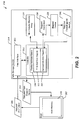
FIG. 1 is a block diagram of a first particular embodiment of a system to map a host access request; -
FIG. 2 is a block diagram of a second particular embodiment of a system to map a host access request; -
FIG. 3 is a diagram illustrating a data address space of a system to map a host access request; -
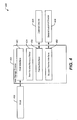
FIG. 4 is a diagram illustrating a particular embodiment of a system to map a host access request to an external device; -
FIG. 5 is a flow diagram of a first particular embodiment of a method of mapping a host access request; -
FIG. 5 is a flow diagram of a first particular embodiment of a method of mapping a host access request; -
FIG. 6 is a flow diagram of a second particular embodiment of a method of mapping a host access request; and -
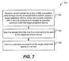
FIG. 7 is a flow diagram of a third particular embodiment of a method of mapping a host access request. - Referring to
FIG. 1 , a particular embodiment of a system to map a host access request is depicted and generally designated 100. Thesystem 100 includes ahost 102 coupled to adata storage device 104. Thedata storage device 104 includes acontroller 122 and adevice address space 130 that includes afirst address region 132 and asecond address region 134. Thecontroller 122 is configured to respond to requests for access to thefirst address region 132 by initiating memory operations at a memory array, such as anon-volatile memory array 124, and to respond to requests for access to thesecond address region 134 by mapping the memory access requests to a mappeddevice 126. Because thefirst address region 132 corresponds to addressable memory at thenon-volatile memory array 124 but thesecond address region 134 may not correspond to addressable memory at thenon-volatile memory array 124, thedevice address space 130 may include a range of addresses that exceeds an addressable amount of memory of thenon-volatile memory array 124. - In a particular embodiment, the
host 102 includes amemory 110 that is addressable by a host memory address space. Thehost 102 may have anoperating system 162. In some embodiments, thehost 102 may also include at least onefile 164 in the host memory address space. Thehost 102 is configured to generate one ormore requests 106 for thedata storage device 104. For example, therequest 106 may send a setting or value to the mappeddevice 126 of thedata storage device 104 or may request a status or value from the mappeddevice 126 of thedata storage device 104. Thehost 102 is further configured to receive data from thedata storage device 104, such as mappeddevice data 108 that includes data generated by the mappeddevice 126. - The
data storage device 104 includes ahost interface 120, thecontroller 122, thenon-volatile memory array 124, and the mappeddevice 126. Thehost interface 120 is adapted to couple thedata storage device 104 to thehost 102. In a particular embodiment, thehost interface 120 includes a universal serial bus (USB) interface that is detachable from thehost 102. Although thehost interface 120 is depicted as separate from thecontroller 122, in other embodiments at least a portion of thehost interface 120 is a component of thecontroller 122. - In a particular embodiment, the
non-volatile memory array 124 includes a flash memory array. Thenon-volatile memory array 124 is addressable via thefirst address region 132 of thedevice address space 130. In a particular embodiment, thedevice address space 130 is independent from the host memory address space. Thedevice address space 130 includes thefirst address region 132 and thesecond address region 134. Thefirst address region 132 is mapped to memory locations of thenon-volatile memory array 124 for data storage and retrieval. For example, a storage request received from thehost 102 to thefirst address region 132 is mapped by thecontroller 122 to a memory storage operation at thenon-volatile memory array 124. Thesecond address region 134 corresponds to the mappeddevice 126 and is distinct from thefirst address region 132. As illustrated, thesecond address region 134 includes a memory address region beyond a useable memory sector of thenon-volatile memory array 124. As used herein, a "usable memory sector" of thenon-volatile memory array 124 is a sector of thenon-volatile memory array 124 that is user visible or user accessible, such as a sector in a public area of thenon-volatile memory array 124 or a sector in a non-public area that is accessible to a user after an authentication or authorization process, as illustrative, non-limiting examples. In a particular embodiment, thefirst address region 132 may correspond to all usable memory sectors (i.e. memory sectors that are user visible or user accessible) of thenon-volatile memory array 124, and no memory addresses within thesecond address region 134 may correspond to a usable location of thememory array 124. In another embodiment, at least one usable sector of thenon-volatile memory array 124 is accessible via thesecond address region 134 but is not accessible via thefirst address region 132. - In a particular embodiment, the
second address region 134 is associated with memory within a hidden storage area. A hidden storage area may include a portion of thenon-volatile memory array 124 that is not usable for storing user data and not visible to thehost 102 as part of a file system. For example, the hidden storage area may include at least one of a U3 hidden area, a TrustedFlash™ hidden area, a TrustedFlash™ Secure Data Object (SDO), and a storage location addressable by an Institute of Electrical and Electronics Engineers IEEE 1667 Silo Command. - The
controller 122 is configured to receive requests from thehost 102 via thehost interface 120 and to control read and write access to thenon-volatile memory array 124. Thecontroller 122 is also configured to selectively map read and write requests from thehost 102 to the mappeddevice 126. For example, when therequest 106 includes a request for write access to thesecond address region 134, thecontroller 122 may be adapted to, in response to therequest 106, direct arequest 136 to the mappeddevice 126 as a request from the host. Therequest 136 may include settings or values to be applied to the mappeddevice 126, such as avalue 160 provided by thehost 102 with therequest 106. As another example, when therequest 106 includes a request for read access to thesecond address region 134, thecontroller 122 may be adapted to, in response to therequest 106, direct therequest 136 to the mappeddevice 126, therequest 136 including a request for data corresponding to the mappeddevice 126. - In a particular embodiment, the
controller 122 is configured to store data received via therequest 106, such as thevalue 160, at thenon-volatile memory array 124 and to provide the stored data to the mappeddevice 126 during an initialization process. For example, thecontroller 122 may store settings for the mappeddevice 126 at a memory location of thenon-volatile memory array 124 that corresponds to thefirst address region 132 or to thesecond address region 134 and may provide the stored settings to the mappeddevice 126 during a power-on process. - The mapped
device 126 provides functionality that is not provided by the universal serial bus (USB) Mass Storage Class access to thefirst address region 132. For example, the mappeddevice 126 may include a user input device, a printer, a scanner, a camera, a buzzer, a light emitting diode (LED), an alarm, a smart card, a temperature sensor, a light sensor, a chemical sensor, an analog-to-digital converting device, a clock, a timer, an accelerometer, a switch, a relay, or a digital-to-analog converting device. In a particular embodiment, the mappeddevice 126 is a bus controller, such as a controller for a Peripheral Component Interconnect (PCI) bus, an Inter-Integrated Circuit (I2C) bus, a OneWire™ bus, a serial bus, a parallel bus, any other bus type, or any combination thereof. - During operation, the
data storage device 104 may be configured to provide a value of the mappeddevice 126 in response to a request for read access to thesecond address region 134 from thehost 102. Thedata storage device 104 may also be configured to set values of the mappeddevice 126 in response to a request for write access to thesecond address region 134 from thehost 102. Thus, thedata storage device 104 may be accessible to thehost 102 as a single endpoint and as a mass storage class (MSC) device by providing access to the mappeddevice 126 via memory mapping. In a USB implementation, thehost 102 can access functionality of thenon-volatile memory array 124 using a MSC device class and can also access non-MSC functionality of the mappeddevice 126 without installing an additional USB device class driver for the mappeddevice 126. USB device classes can utilize multiple logical channels or "pipes" for communication, with each pipe assigned to a corresponding endpoint at the USB device. In USB implementations, a total number of pipes available to a device may be limited, and each pipe may require a buffer at thehost 102 or at thedata storage device 104 to buffer data for transport via the USB bus. By implementing a MSC device class for thedata storage device 104 and enabling access to the mappeddevice 126 via memory mapping, a number of pipes, device drivers, and buffers may be reduced as compared to implementing multiple device classes. - To illustrate, in a particular embodiment, when the
request 106 is a write request including thevalue 160 to be written to thesecond address region 134, thecontroller 122 uses thevalue 160 to adjust one or more parameters of the mappeddevice 126. When therequest 106 is a read request to read thesecond address region 134, thecontroller 122 interprets therequest 106 as an instruction to read data from the mappeddevice 126 and sends therequest 136 to the mapped device. The mappeddevice 126 may provide a value of the mappeddevice 126 as mappeddevice data 138 in response to the readrequest 136. - For example, a value that is provided as mapped
device data 138 may include a status indicator, a switch setting, or any other device information. The mappeddevice data 138 may be provided to thecontroller 122 from the mappeddevice 126, and thecontroller 122 may be configured to send the mappeddevice data 138 as the mappeddevice data 108 to thehost 102. - In another embodiment, the mapped
device data 138 may be stored at thenon-volatile memory array 124. For example, in an embodiment where thesecond address region 134 is associated with usable memory of thenon-volatile memory array 124, the mappeddevice data 138 may be stored at thesecond address region 134 to be retrieved by thehost 102 via a memory read request to access thesecond address region 134. As another example, such as when thesecond address region 134 does not correspond to usable memory, the mappeddevice data 138 may be stored at thefirst address region 132. The location of the mappeddevice data 138 at thefirst address region 132 may be known by thehost 102 and accessible via a memory read request to the specific location initiated by thehost 102. Alternatively, thecontroller 122 may manage retrieval of the mappeddevice data 138 from thefirst address region 132 in a manner that is transparent to thehost 102. - In a particular embodiment, the
second address region 134 is accessed indirectly by thehost 102 using thefile 164. Thefile 164 may be associated with thesecond address region 134 by theoperating system 162 of thehost 102. In another embodiment, thesecond address region 134 is accessed directly by thehost 102 without use of thefile 164. - In a particular implementation, a command from the
host 102 is mapped by thecontroller 122 to the mappeddevice 126 which is external to thenon-volatile memory array 124. The command may be communicated in compliance with a security protocol, and thecontroller 122 receives an identifier associated with the mappeddevice 126 device from thehost 102. In a particular embodiment, the security protocol is a small computer system interface (SCSI) protocol. The command may be compliant with Institute of Electrical and Electronics Engineers IEEE Std. 1667. - For example, the
data storage device 104 may include an Addressable Content Target (ACT) that includes a first silo compliant with IEEE 1667. A probe command may return a silo type identifier for each silo implemented in the ACT to thehost 102, including a silo type identifier for a second silo that is used for the mappeddevice 126. Thehost 102 can determine the presence of the mappeddevice 126 via the silo type identifier of the second silo and can further determine commands defined for the silo type to provide an interface to access theSecond Address Region 134. - In a SCSI security protocol implementation, the
host 102 may generate therequest 106 including a SCSI Security Protocol Out command identifying the silo of the mapped device, a device command that is supported by the silo type, and may include one or more values such as thevalue 160. Thecontroller 122 may interpret therequest 106 and provide the device command to the mappeddevice 126 via therequest 136. Thehost 102 may also send a SCSI Security Protocol In command to thedata storage device 104. The Security Protocol In command may be interpreted by thecontroller 122 as a request to read the mappeddevice data 138 that is provided in response to the device command. Thecontroller 122 may initiate sending the mappeddevice data 108 to thehost 102 in a format specified by the silo type of the mappeddevice 126. In an embodiment where thedata storage device 104 includes or supports multiple devices such as peripherals, thenon-volatile memory array 124 may include multiple silo types associated with the devices to enable access by thehost 102 and/or a single silo type associated with multiple devices. - As will be discussed with respect to
FIG. 3 , thedevice address space 130 may further include one or more additional address regions. For example, thedevice address space 130 may include a third address region, and a request from thehost 102 to access the third address region may be mapped by thecontroller 122 to a second mapped device. As will be discussed with respect toFIG. 4 , the mappeddevice 126 may be a first external device that is coupled to thedata storage device 104 via a device interface, and the second mapped device may be a second external device that is coupled to thedata storage device 104 via a second device interface. - By enabling host access to the
non-volatile memory array 124 and also enabling host access to the mappeddevice 126 by mapping access requests for thesecond address region 134 to the mappeddevice 126, multiple components of thedata storage device 102 of different device classes are accessible to thehost 102 using a single connection endpoint For example, in a USB implementation, both thenon-volatile memory array 124 and the mappeddevice 126 are accessible via a single MSC device interface. Such an implementation may reduce a number of USB endpoints and buffers that may be required to support the mappeddevice 126 as a separate USB class. - Referring to
FIG. 2 , a second particular embodiment of a system to map a host access request is depicted and generally designated 200. Thesystem 200 includes ahost 202 coupled to adata storage device 204. Thehost 202 includes ahost memory 210 that is addressable by a host memory address space. Thedata storage device 204 includes adevice address space 230 that is independent from the host memory address space. Thedevice address space 230 includes afirst address region 232 that is mapped to anon-volatile memory array 224 and asecond address region 234 that is mapped to a mappeddevice 226. In a particular embodiment, one or more components of thesystem 200 may operate substantially similarly to corresponding components of thesystem 100 ofFIG. 1 . - The mapped
device 226 is accessible to thehost 202 via arequest 206 to access thesecond address region 234. Acontroller 222 is configured to identify therequest 206 as a write or read request to thesecond address region 234 and to send arequest 236 to the mappeddevice 226. When therequest 206 is a write request, therequest 236 may set parameters of the mappeddevice 226. When therequest 206 is a read request, therequest 236 may indicate a request for a value of settings or other data from the mappeddevice 226. - The mapped
device 226 is configured to generate arequest 240 to be sent to thehost 202. Therequest 240 may include a request to access thesecond address region 234. Therequest 240 may be mapped by thecontroller 222 to thehost 202, and thecontroller 222 may initiate sending arequest 242 to thehost 202 via ahost interface 220. Therequest 242 may correspond to therequest 240. - In a particular embodiment, the
request 240 may be stored at thenon-volatile memory array 224 to be accessed by thehost 202 during a memory read request. In another embodiment, such as where thehost interface 220 includes a USB 3.0 interface that enables USB devices to send requests to a USB host, therequest 240 may be provided by the mappeddevice 226 to thecontroller 222, and thecontroller 222 may initiate sending therequest 242 thehost 202 via thehost interface 220. - Referring to
FIG. 3 , a particular embodiment of a system to map a memory request is depicted and generally designated 300. Thesystem 300 includes adata address space 302 including afirst address region 304, asecond address region 306, and athird address region 308. Thefirst address region 304 may include a range of addresses corresponding to usable physical memory in a data storage device, such as thedata storage device 104 ofFIG. 1 or thedata storage device 204 ofFIG. 2 . Thesecond address region 306 and thethird address region 308 are past a lastusable memory address 310. - The
second address region 306 may be mapped by a memory controller as corresponding to a particular device that is external to the physical memory, such as the mappeddevice 126 ofFIG. 1 or the mappeddevice 226 ofFIG. 2 . Similarly, thethird address region 308 may be identified by a memory controller as being mapped to a second device. AlthoughFIG. 3 depicts asecond address region 306 and athird address region 308, in other embodiments the data addressspace 302 may include a single address region past the lastusable memory address 310, or three or more address regions beyond the lastusable memory address 310. - In a USB implementation, the data address
space 302 may correspond to a memory device that is accessed via a USB MSC device interface. Multiple devices that are external to the memory may be mapped such that they are accessible by a host device without being added as USB devices. - Referring to
FIG. 4 , a particular embodiment of a system to map a host access request is depicted and generally designated 400. Thesystem 400 includes ahost 402 coupled to adata storage device 404. Thedata storage device 404 is coupled to anexternal device 406 and to a secondexternal device 408, such as one or more peripheral devices. In an illustrative embodiment, thedata storage device 404 is thedata storage device 104 ofFIG. 1 or thedata storage device 204 ofFIG. 2 . - In a particular embodiment, the
data storage device 404 includes ahost interface 420, anon-volatile memory array 424, adevice interface 450, and asecond device interface 452. Thehost interface 420 is configured to couple thedata storage device 404 to thehost 402. Thehost interface 420 is also configured to enable thehost 402 to send memory access requests to thedata storage device 404. Thehost interface 420 is further configured to provide data to thehost 402, such as data retrieved from thenon-volatile memory array 424, data retrieved via thedevice interface 450, or data retrieved via thesecond device interface 452. In a particular embodiment, thehost interface 420 includes a USB interface that is adapted to detachably couple thedata storage device 404 to thehost 402. - In a particular embodiment, the
device interface 450 is adapted to couple to theexternal device 406, and thesecond device interface 452 is adapted to couple to the secondexternal device 408. Thehost interface 420 may implement a USB interface and thedata storage device 404 may enable thehost 402 to access theexternal device 406 and the secondexternal device 408 by mapping access requests to thenon-valatile memory array 424. Thus, thedevice interface 450 and thesecond device interface 452 do not represent USB endpoints. - In a particular embodiment, the
data storage device 404 is configured to map commands from thehost 402 to thenon-volatile memory array 424, or to theexternal device 406 or the secondexternal device 408, without implementing the firstexternal device 406 and the secondexternal device 408 as additional USB devices. For example, the firstexternal device 406 and the secondexternal device 408 may be accessed by memory access requests sent from thehost 402 to address ranges that are mapped to the firstexternal device 406 and the secondexternal device 408, respectively. For example, thenon-volatile memory array 424 may be addressable by the data addressspace 302 ofFIG. 3 such that theexternal device 406 is accessible via an access request to thesecond address region 306 and the secondexternal device 408 is accessible via an access request to thethird address region 308. - Referring to
FIG. 5 , a first particular embodiment of a method of mapping a host access request is depicted and generally designated 500. In a particular embodiment, themethod 500 may be performed by thedata storage device 104 ofFIG. 1 , thedata storage device 204 ofFIG. 2 , or thedata storage device 404 ofFIG. 4 . - At 502, a request from a host to access a flash memory address region associated with a peripheral device is received at a Universal Serial Bus (USB) flash device. For example, the flash memory address region may correspond to the
second address region 134 of thedata storage device 104 ofFIG. 1 , and the peripheral device may correspond to the mappeddevice 126 ofFIG. 1 . In another particular embodiment, the peripheral device may correspond to theexternal device 406 ofFIG. 4 . - Advancing to 504, the request from the host to access the flash memory address region associated with the peripheral device is mapped to the peripheral device. For example, when the request is a write request, the request may be mapped as a command sent to the peripheral device to set parameters at the peripheral device. As another example, when the request is a read request, the request may be mapped as a command sent to the peripheral device to read configuration or status information of the peripheral device.
- Thus, the host can access the peripheral device using requests to access a memory within the device address space, and the requests are mapped to the peripheral device. As a result, a USB device interface for the peripheral device need not be supported to enable access by the host.
- Referring to
FIG. 6 , a second particular embodiment of a method of mapping a host access request is depicted and generally designated 600. Themethod 600 includes, at 602, receiving, at a Universal Serial Bus (USB) flash device, a request from a host to access a flash memory address region associated with a peripheral device. The USB flash device includes a memory array associated with a memory array address space. The flash memory address region associated with the peripheral device is outside the memory array address space. For example, the request may be received at thedata storage device 104 ofFIG. 1 , thedata storage device 204 ofFIG. 2 , or thedata storage device 404 ofFIG. 4 . - Advancing to 604, the request from the host to access the flash memory address region associated with the peripheral device is mapped to the peripheral device. In a particular embodiment, the flash memory address region associated with the peripheral device is accessible to the host as a single end point and as a mass storage class (MSC) device.
- Moving to 606, a request from the peripheral device to access the flash memory address region associated with the peripheral device may be received at the USB flash device. Proceeding to 608, the request from the peripheral device to access the flash memory address region associated with the peripheral device may be mapped to the host. In a particular embodiment, the request from the peripheral device is the
request 240 that is mapped to host 202 via therequest 242 ofFIG. 2 . - Continuing to 610, one or more settings associated with the peripheral device may be stored at the USB flash device at the flash memory address region associated with the peripheral device. Advancing to 612, the USB flash device may be detached from the host, and moving to 614, the USB flash device may be attached to a second host. Proceeding to 616, a request from the second host to access the flash memory address region associated with the peripheral device may be received at the USB flash device. Continuing to 618, the request from the second host to access the flash memory address region associated with the peripheral device may be mapped to the peripheral device. Thus, the USB flash device may enable multiple hosts to access the peripheral device by mapping requests to access the flash memory address region associated with the peripheral device.
- Referring to
FIG. 7 , a third illustrative embodiment of a method of mapping a host access request is depicted and generally designated 700. At 702, a request from a host to access a target peripheral device is received at a Universal Serial Bus (USB) compatible data storage device, where the request conforms with a security protocol and includes an identifier associated with the target peripheral device. The data storage device may be a mass storage device, such as a flash device. - The security protocol may be small computer system interface (SCSI) compatible. For example, the request from the host may include one of an In command and an Out command of a small computer system interface (SCSI) security protocol. The request may be compliant with Institute of Electrical and Electronics Engineers IEEE Std. 1667.
- In a particular embodiment, the identifier is a silo type identifier. The identifier may indicate a silo type corresponding to a type of the target peripheral device. For example, the silo type may correspond to a light emitting diode (LED).
- Continuing to 704, the request from the host is mapped to a command to be sent to the target peripheral device. Advancing to 706, data received from the target peripheral device is communicated to the host. The data may be communicated using an Out command a SCSI security protocol.
- By using the request conforming with the security protocol, the host may communicate with the target peripheral device via the data storage device without the data storage device implementing a USB device interface for the target peripheral device. For example, the data storage device may be a flash memory device that is accessible to the host as a single endpoint and as a mass storage class (MSC) device, while enabling the host to access the target peripheral device.
- Although various components depicted herein are illustrated as block components and described in general terms, such components may include one or more microprocessors, state machines, or other circuits configured to enable the
data storage device 104 ofFIG. 1 or thedata storage device 204 ofFIG. 2 to perform the particular functions attributed to such components, or any combination thereof. For example, thehost interface 120, thecontroller 122, or both, ofFIG. 1 may represent physical components, such as controllers, state machines, logic circuits, or other structures to enable thedata storage device 104 to receive and respond to data requests from a host device or from other external devices by mapping the host requests to thesecond address region 134 to the mappeddevice 126. - For example, the
controller 122 ofFIG. 1 may be implemented using a microprocessor or microcontroller programmed to determine whether a memory access request from a host corresponds to thesecond address region 134 and to send the request to the mappeddevice 126 when the request corresponds to thesecond address region 134. In a particular embodiment, thecontroller 122 ofFIG. 1 includes executable instructions that are executed by a processor and the instructions are stored at thememory array 124. Alternatively, or in addition, executable instructions that are executed by the processor may be stored at a separate memory location that is not part of thememory array 104, such as at a read-only memory (ROM) (not shown) at thecontroller 122. - In a particular embodiment, the
data storage device 104 may be a portable device configured to be selectively coupled to one or more external devices. However, in other embodiments, the data storage device may be attached or embedded within one or more host devices, such as within a housing of a portable communication device. For example, the data storage device may be within a packaged apparatus such as a wireless telephone, personal digital assistant (PDA), gaming device or console, portable navigation device, or other device that uses internal non-volatile memory. In a particular embodiment, thedata storage device 104 includes a non-volatile memory, such as a flash memory (e.g., NAND, NOR, Multi-Level Cell (MLC), Divided bit-line NOR (DINOR), AND, high capacitive coupling ratio (HiCR), asymmetrical contactless transistor (ACT), or other flash memories), an erasable programmable read-only memory (EPROM), an electrically-erasable programmable read-only memory (EEPROM), a read-only memory (ROM), a one-time programmable memory (OTP), or any other type of memory. - The illustrations of the embodiments described herein are intended to provide a general understanding of the structure of the various embodiments. The illustrations are not intended to serve as a complete description of all of the elements and features of apparatus and systems that utilize the structures or methods described herein. Many other embodiments may be apparent to those of skill in the art upon reviewing the disclosure. Other embodiments may be utilized and derived from the disclosure, such that structural and logical substitutions and changes may be made without departing from the scope of the disclosure. Although specific embodiments have been illustrated and described herein, it should be appreciated that any subsequent arrangement designed to achieve the same or similar purpose may be substituted for the specific embodiments shown. This disclosure is intended to cover any and all subsequent adaptations or variations of various embodiments. Combinations of the above embodiments, and other embodiments not specifically described herein, will be apparent to those of skill in the art upon reviewing the description. Accordingly, the disclosure and the figures are to be regarded as illustrative rather than restrictive.
- The Abstract of the Disclosure is submitted with the understanding that it will not be used to interpret or limit the scope or meaning of the claims. In addition, in the foregoing Detailed Description, various features may be grouped together or described in a single embodiment for the purpose of streamlining the disclosure. This disclosure is not to be interpreted as reflecting an intention that the claimed embodiments require more features than are expressly recited in each claim. Rather, as the following claims reflect, inventive subject matter may be directed to less than all of the features of any of the disclosed embodiments.
- The above-disclosed subject matter is to be considered illustrative, and not restrictive, and the appended claims are intended to cover all such modifications, enhancements, and other embodiments, which fall within the scope of the present disclosure. Thus, to the maximum extent allowed by law, the scope of the present invention is to be determined by the broadest permissible interpretation of the following claims and their equivalents, and shall not be restricted or limited by the foregoing detailed description.
- Further embodiments are set out in the following clauses:
- 1. A data storage device, comprising: a host interface, wherein the host interface is adapted to couple the data storage device to a host, the host including memory that is addressable by a host memory address space; a device address space that is independent from the host memory address space, the device address space including a first address region and a second address region, wherein the second address region is distinct from the first address region; a non-volatile memory array; and a controller coupled to the non-volatile memory array and further coupled to a mapped device, wherein the controller is adapted to, in response to a first request from the host for access to the first address region of the device address space, perform a memory access operation at the non-volatile memory array, and wherein the controller is further adapted to, in response to a second request from the host for access to the second address region of the device address space, map the second request to the mapped device.
- 2. The data storage device of clause 1, wherein the data storage device provides a value of the mapped device in response to a request for read access to the second address region.
- 3. The data storage device of clause 2, the controller uses the value to adjust one or more parameters of the mapped device in response to a request for write access to the second address region.
- 4. The data storage device of clause 3, wherein the controller is configured to store data received via the request for write access to the second address region at the non-volatile memory and to provide the stored data to the mapped device during an initialization process.
- 5. The data storage device of clause 1, wherein a request from the mapped device to access the second address region is mapped by the controller to the host.
- 6. The data storage device of clause 1, wherein the host interface includes a Universal Serial Bus (USB) interface that is detachable from the host.
- 7. The data storage device of clause 1, wherein the non-volatile memory array includes a flash memory array.
- 8. The data storage device of clause 1, wherein the data storage device is accessible to the host as a single endpoint and as a mass storage class (MSC) device.
- 9. The data storage device of clause 1, wherein the first address region is adapted to store data, and wherein a storage request is mapped by the controller to the first address region.
- 10. The data storage device of clause 1, wherein the second address region includes a useable memory sector of the non- volatile memory array.
- 11. The data storage device of clause 1, wherein the second address region includes a memory address region beyond a useable memory sector of the non-volatile memory array.
- 12. The data storage device of clause 1, wherein the second address region is associated with memory within a hidden storage area.
- 13. The data storage device of clause 12, wherein the hidden storage area includes at least one of a U3 hidden area, a TrustedFlash hidden area, a TrustedFlash secure data object (SDO), and a storage location addressable by an Institute of Electrical and Electronics Engineers IEEE 1667 Silo Command.
- 14. The data storage device of clause 1, wherein the second address region is accessed directly by the host.
- 15. The data storage device of clause 1, wherein the second address region is accessed indirectly by the host using at least one file associated with the second address region by an operating system of the host.
- 16. The data storage device of clause 1, wherein the device address space further comprises a third address region, and wherein a request from the host to access the third address region is mapped by the controller to a second mapped device.
- 17. The data storage device of clause 16, wherein the mapped device is a first external device that is coupled to the data storage device via a device interface, and wherein the second mapped device is a second external device that is coupled to the data storage device via a second device interface.
- 18. The data storage device of clause 1, wherein the mapped device is associated with a Universal Serial Bus (USB) class other than a mass storage class.
- 19. The data storage device of clause 18, wherein the mapped device includes one of a user input device, a printer, a scanner, a camera, a buzzer, a light emitting diode (LED), an alarm, a smart card, a temperature sensor, a light sensor, a chemical sensor, an analog-to-digital converting device, a clock, a timer, an accelerometer, a switch, a relay, and a digital-to-analog converting device.
- 20. The data storage device of clause 18, wherein the mapped device is a bus controller.
- 21. An apparatus comprising a controller, wherein the controller is configured to be coupled to a non-volatile memory array addressable by a first address region of a device address space that is independent from a host memory address space, the device address space including the first address region and a second address region; wherein the controller is configured to receive a request to access the second address region from a host via a host interface; and wherein the controller is configured to map the request to a device that is external to the non-volatile memory array.
- 22. The apparatus of clause 21, further comprising the non-volatile memory array coupled to the controller.
- 23. A method, comprising: receiving, at a Universal Serial Bus (USB) flash device, a request from a host to access a flash memory address region associated with a peripheral device, wherein the USB flash device includes a memory array associated with a memory array address space, and wherein the flash memory address region associated with the peripheral device is outside the memory array address space; and mapping the request from the host to access the flash memory address region associated with the peripheral device to the peripheral device.
- 24. The method of clause 23, wherein the flash memory address region associated with the peripheral device is accessible to the host as a single endpoint and as a mass storage class (MSC) device.
- 25. The method of clause 23, further comprising: receiving, at the USB flash device, a request from the peripheral device to access the flash memory address region associated with the peripheral device; and mapping the request from the peripheral device to access the flash memory address region associated with the peripheral device to the host.
- 26. The method of clause 23, further comprising storing one or more settings associated with the peripheral device at the USB flash device at the flash memory address region associated with the peripheral device.
- 27. The method of clause 26, further comprising: detaching the USB flash device from the host; attaching the USB flash device to a second host; receiving, at the USB flash device, a request from the second host to access the flash memory address region associated with the peripheral device; and mapping the request from the second host to access the flash memory address region associated with the peripheral device to the peripheral device.
- 28. A detachable Universal Serial Bus (USB) flash device, comprising: a USB interface adapted to couple the detachable USB flash device to a host, the host including memory that is addressable by a host memory address space; a device interface adapted to couple the detachable USB flash device to a peripheral device, wherein the device interface is different from the host interface; a flash memory array associated with a first address region of a device address space; and a controller coupled to the flash memory array; wherein the controller is adapted to, in response to a request from the host to access a second address region of the device address space, map the request from the host to the peripheral device via the device interface, wherein the second address region is distinct from the first address region, and wherein the controller is further adapted to, in response to a request from the peripheral device to access the second address region, map the request from the peripheral device to the host via the USB interface.
- 29. A method comprising: receiving, at a universal serial bus (USB) compatible data storage device, a request from a host to access a target peripheral device, wherein the request conforms with a security protocol and includes an identifier associated with the target peripheral device, wherein the data storage device is a mass storage device; and mapping the request from the host to a command to be sent to the target peripheral device.
- 30. The method of clause 29, wherein the identifier is a silo type identifier.
- 31. The method of clause 29, wherein the request is compliant with Institute of Electrical and Electronics Engineers IEEE Std. 1667.
- 32. The method of clause 29, wherein the security protocol is small computer system interface (SCSI) compatible.
- 33. The method of clause 29, further comprising communicating data received from the target peripheral device to the host.
- 34. The method of clause 33, wherein the data is communicated using an Out command of a small computer system interface (SCSI) security protocol.
- 35. The method of clause 29, wherein the command from the host includes one of an In command and an Out command of a small computer system interface (SCSI) security protocol.
- 36. The method of clause 35, wherein the identifier indicates a silo type corresponding to a type of the target peripheral device.
- 37. The method of clause 36, wherein the silo type corresponds to a light emitting diode (LED).
- 38. The method of clause 29, wherein the data storage device is a flash memory device that is accessible to the host as a single endpoint and as a mass storage class (MSC) device.
- 39. A data storage device, comprising: a host interface, wherein the host interface is adapted to couple the data storage device to a host; a non-volatile memory array; and a controller coupled to the non-volatile memory array; wherein the controller is configured to map a command from the host to an external device, wherein the command is communicated in compliance with a security protocol and wherein the controller receives an identifier associated with the external device from the host.
- 40. The data storage device of clause 39, wherein the data storage device is a mass storage device and wherein the external device has a class of human interface device (HID).
Claims (15)
- A method comprising:receiving, at a universal serial bus compatible data storage device (104), a request (106) from a host to access a mapped device (126), wherein the request conforms with a security protocol and includes an identifier associated with the mapped device (126), wherein the data storage device is a mass storage device; andmapping the request (106) from the host to a command to be sent to the mapped device (126).
- The method of claim 1, wherein the identifier is a silo type identifier.
- The method of claim 1, wherein the request is compliant with Institute of Electrical and Electronics Engineers IEEE Std. 1667.
- The method of claim 1, wherein the security protocol is small computer system interface compatible.
- The method of claim 1, further comprising communicating data received from the mapped device to the host.
- The method of claim 5, wherein the data is communicated using an Out command of a small computer system interface security protocol.
- The method of claim 1, wherein the command from the host includes one of an In command and an Out command of a small computer system interface security protocol.
- The method of claim 7, wherein the identifier indicates a silo type corresponding to a type of the mapped device.
- The method of claim 8, wherein the silo type corresponds to a light emitting diode.
- The method of claim 1, wherein the data storage device is a flash memory device that is accessible to the host as a single endpoint and as a mass storage class device.
- The method of claim 1, wherein the mapped device is an external device that is coupled to the data storage device via a device interface.
- A data storage device (404), comprising:a host interface (420), wherein the host interface (420) is adapted to couple the data storage device (404) to a host (402);a non-volatile memory (424); anda controller coupled to the non-volatile memory (424);wherein the controller is configured to map a command from the host (402) to an external device (406), wherein the command is communicated in compliance with a security protocol and wherein the controller receives an identifier associated with the external device (406) from the host (402).
- The data storage device of claim 12, wherein the data storage device is a mass storage device and wherein the external device has a class of human interface device.
- The data storage device of claim 12, wherein the identifier is a silo type identifier.
- The data storage device of claim 12, wherein the external device is coupled to the data storage device via a device interface.
Applications Claiming Priority (2)
| Application Number | Priority Date | Filing Date | Title |
|---|---|---|---|
| US12/369,408 US8386723B2 (en) | 2009-02-11 | 2009-02-11 | System and method of host request mapping |
| EP10700774.2A EP2396728B1 (en) | 2009-02-11 | 2010-01-08 | System and method of host request mapping |
Related Parent Applications (2)
| Application Number | Title | Priority Date | Filing Date |
|---|---|---|---|
| EP10700774.2A Division-Into EP2396728B1 (en) | 2009-02-11 | 2010-01-08 | System and method of host request mapping |
| EP10700774.2 Division | 2010-01-08 |
Publications (2)
| Publication Number | Publication Date |
|---|---|
| EP2426607A2 true EP2426607A2 (en) | 2012-03-07 |
| EP2426607A3 EP2426607A3 (en) | 2012-03-28 |
Family
ID=42246348
Family Applications (2)
| Application Number | Title | Priority Date | Filing Date |
|---|---|---|---|
| EP11187453A Withdrawn EP2426607A3 (en) | 2009-02-11 | 2010-01-08 | System and method of host request mapping |
| EP10700774.2A Not-in-force EP2396728B1 (en) | 2009-02-11 | 2010-01-08 | System and method of host request mapping |
Family Applications After (1)
| Application Number | Title | Priority Date | Filing Date |
|---|---|---|---|
| EP10700774.2A Not-in-force EP2396728B1 (en) | 2009-02-11 | 2010-01-08 | System and method of host request mapping |
Country Status (6)
| Country | Link |
|---|---|
| US (1) | US8386723B2 (en) |
| EP (2) | EP2426607A3 (en) |
| KR (1) | KR20110117134A (en) |
| CN (1) | CN102301348B (en) |
| TW (1) | TW201032054A (en) |
| WO (1) | WO2010093487A2 (en) |
Cited By (1)
| Publication number | Priority date | Publication date | Assignee | Title |
|---|---|---|---|---|
| CN107526695A (en) * | 2016-06-20 | 2017-12-29 | 北京忆芯科技有限公司 | NVMe configuration spaces implementation method and device |
Families Citing this family (35)
| Publication number | Priority date | Publication date | Assignee | Title |
|---|---|---|---|---|
| US9092387B2 (en) * | 2008-12-10 | 2015-07-28 | Micron Technology, Inc. | Non-volatile memory device capable of initiating transactions |
| WO2011026530A1 (en) * | 2009-09-07 | 2011-03-10 | Tomtom International B.V. | Navigation apparatus and method of supporting hands-free voice communication |
| US8301824B2 (en) * | 2010-07-22 | 2012-10-30 | Sandisk Il Ltd. | Using an add-on storage device for extending the storage capacity of a storage device |
| US8296495B2 (en) * | 2010-07-22 | 2012-10-23 | Sandisk Il Ltd. | Using an add-on storage device for extending the storage capacity of a storage device in a host device |
| TWI451247B (en) * | 2010-09-23 | 2014-09-01 | Phison Electronics Corp | Data writing method, memory controller and memory storage apparatus |
| US8738843B2 (en) * | 2010-12-20 | 2014-05-27 | Lsi Corporation | Data manipulation during memory backup |
| JP5734492B1 (en) * | 2014-05-08 | 2015-06-17 | ウィンボンド エレクトロニクス コーポレーション | Semiconductor memory device |
| WO2016178706A1 (en) * | 2015-05-02 | 2016-11-10 | Hewlett Packard Enterprise Development Lp | Storage memory direct access |
| US20170255565A1 (en) * | 2016-03-02 | 2017-09-07 | Intel Corporation | Method and apparatus for providing a contiguously addressable memory region by remapping an address space |
| CN112347012B (en) * | 2016-06-20 | 2024-07-23 | 北京忆芯科技有限公司 | NVMe controller and method supporting SR-IOV |
| FR3055715B1 (en) * | 2016-09-08 | 2018-10-05 | Upmem | METHODS AND DEVICES FOR CONTOURING INTERNAL CACHE OF ADVANCED DRAM MEMORY CONTROLLER |
| US10176108B2 (en) * | 2016-09-30 | 2019-01-08 | Intel Corporation | Accessing memory coupled to a target node from an initiator node |
| CN108073360B (en) * | 2016-11-15 | 2024-01-23 | 三星电子株式会社 | Computing device including storage device and method of operating computing device |
| US10515007B2 (en) * | 2017-03-31 | 2019-12-24 | Intel Corporation | Technologies for remapping pending bit array read requests |
| US10497438B2 (en) * | 2017-04-14 | 2019-12-03 | Sandisk Technologies Llc | Cross-point memory array addressing |
| CN113165395B (en) | 2018-12-03 | 2023-01-10 | 惠普发展公司,有限责任合伙企业 | logic circuit system |
| EP3688645A1 (en) | 2018-12-03 | 2020-08-05 | Hewlett-Packard Development Company, L.P. | Logic circuitry package |
| PT3681723T (en) | 2018-12-03 | 2021-08-27 | Hewlett Packard Development Co | Logic circuitry |
| BR112021010672A2 (en) | 2018-12-03 | 2021-08-24 | Hewlett-Packard Development Company, L.P. | logic circuits |
| EP3695334A1 (en) | 2018-12-03 | 2020-08-19 | Hewlett Packard Enterprise Development Company LP | Logic circuitry |
| CA3121146C (en) | 2018-12-03 | 2024-05-28 | Hewlett-Packard Development Company, L.P. | Logic circuitry package for controlling ic2 traffic |
| CN113168453A (en) | 2018-12-03 | 2021-07-23 | 惠普发展公司,有限责任合伙企业 | Logic circuitry packaging |
| PL3682359T3 (en) | 2018-12-03 | 2021-05-17 | Hewlett-Packard Development Company, L.P. | Logic circuitry |
| US11338586B2 (en) | 2018-12-03 | 2022-05-24 | Hewlett-Packard Development Company, L.P. | Logic circuitry |
| US10894423B2 (en) | 2018-12-03 | 2021-01-19 | Hewlett-Packard Development Company, L.P. | Logic circuitry |
| US11038749B2 (en) * | 2018-12-24 | 2021-06-15 | Intel Corporation | Memory resource allocation in an end-point device |
| US11257543B2 (en) * | 2019-06-25 | 2022-02-22 | Stmicroelectronics International N.V. | Memory management device, system and method |
| US11360667B2 (en) | 2019-09-09 | 2022-06-14 | Stmicroelectronics S.R.L. | Tagged memory operated at lower vmin in error tolerant system |
| US11407229B2 (en) | 2019-10-25 | 2022-08-09 | Hewlett-Packard Development Company, L.P. | Logic circuitry package |
| WO2021221678A1 (en) | 2020-04-30 | 2021-11-04 | Hewlett-Packard Development Company, L.P. | Logic circuitry package for print apparatus |
| CN114063879B (en) * | 2020-07-31 | 2024-04-09 | 伊姆西Ip控股有限责任公司 | Method for processing operation command, electronic device and storage medium |
| US20230073503A1 (en) * | 2021-09-07 | 2023-03-09 | Micron Technology, Inc. | Security file system for a memory system |
| US12541307B2 (en) * | 2021-11-08 | 2026-02-03 | Ambiq Micro, Inc. | Flexible and low power cache memory architecture |
| CN114328358A (en) * | 2022-03-04 | 2022-04-12 | 山东华翼微电子技术股份有限公司 | Method for accessing random-capacity memory by 7-bit addressing mode I2C controller |
| KR20240086021A (en) * | 2022-12-09 | 2024-06-18 | 에스케이하이닉스 주식회사 | Controller, storage device and method for oprating thereof being capable of reducing degradation of memory |
Family Cites Families (11)
| Publication number | Priority date | Publication date | Assignee | Title |
|---|---|---|---|---|
| US6327640B1 (en) * | 1997-03-07 | 2001-12-04 | Advanced Micro Devices, Inc. | Overlapping peripheral chip select space with DRAM on a microcontroller with an integrated DRAM controller |
| US6148354A (en) * | 1999-04-05 | 2000-11-14 | M-Systems Flash Disk Pioneers Ltd. | Architecture for a universal serial bus-based PC flash disk |
| CN1151415C (en) * | 2001-10-23 | 2004-05-26 | 深圳市朗科科技有限公司 | Method for adding additional memory function to periphrals of computer and its architecture |
| US7334077B2 (en) * | 2003-10-17 | 2008-02-19 | Renesas Technology America, Inc. | Method and apparatus for smart memory pass-through communication |
| US8135363B2 (en) * | 2005-02-12 | 2012-03-13 | Broadcom Corporation | Method and system for an integrated circuit supporting auto-sense of voltage for drive strength adjustment |
| US7409489B2 (en) * | 2005-08-03 | 2008-08-05 | Sandisk Corporation | Scheduling of reclaim operations in non-volatile memory |
| US20070136501A1 (en) * | 2005-12-08 | 2007-06-14 | Chang Robert C | Media card command pass through methods |
| BRPI0712109A8 (en) | 2006-05-29 | 2016-03-29 | Papagrigoriou Paschalis | METHOD FOR COMMUNICATION WITH A MULTIFUNCTIONAL MEMORY CARD |
| DE102006054025A1 (en) | 2006-11-16 | 2008-05-21 | Giesecke & Devrient Gmbh | Data storage device with additional function |
| US20080293449A1 (en) * | 2007-05-24 | 2008-11-27 | Stephen Barlow | Method and system for partitioning a device into domains to optimize power consumption |
| US20090077273A1 (en) * | 2007-09-18 | 2009-03-19 | Barinder Singh Rai | Control Data Transfer |
-
2009
- 2009-02-11 US US12/369,408 patent/US8386723B2/en not_active Expired - Fee Related
-
2010
- 2010-01-08 EP EP11187453A patent/EP2426607A3/en not_active Withdrawn
- 2010-01-08 WO PCT/US2010/020527 patent/WO2010093487A2/en not_active Ceased
- 2010-01-08 KR KR1020117018191A patent/KR20110117134A/en not_active Withdrawn
- 2010-01-08 CN CN201080005925.5A patent/CN102301348B/en not_active Expired - Fee Related
- 2010-01-08 EP EP10700774.2A patent/EP2396728B1/en not_active Not-in-force
- 2010-01-18 TW TW099101235A patent/TW201032054A/en unknown
Non-Patent Citations (1)
| Title |
|---|
| None |
Cited By (2)
| Publication number | Priority date | Publication date | Assignee | Title |
|---|---|---|---|---|
| CN107526695A (en) * | 2016-06-20 | 2017-12-29 | 北京忆芯科技有限公司 | NVMe configuration spaces implementation method and device |
| CN107526695B (en) * | 2016-06-20 | 2021-03-02 | 北京忆芯科技有限公司 | NVMe configuration space implementation method and device |
Also Published As
| Publication number | Publication date |
|---|---|
| KR20110117134A (en) | 2011-10-26 |
| CN102301348A (en) | 2011-12-28 |
| EP2396728A2 (en) | 2011-12-21 |
| CN102301348B (en) | 2014-10-15 |
| WO2010093487A2 (en) | 2010-08-19 |
| US20100205350A1 (en) | 2010-08-12 |
| EP2426607A3 (en) | 2012-03-28 |
| US8386723B2 (en) | 2013-02-26 |
| TW201032054A (en) | 2010-09-01 |
| WO2010093487A3 (en) | 2010-12-16 |
| EP2396728B1 (en) | 2014-07-23 |
Similar Documents
| Publication | Publication Date | Title |
|---|---|---|
| US8386723B2 (en) | System and method of host request mapping | |
| USRE50101E1 (en) | Memory system in which extended function can easily be set | |
| KR101395778B1 (en) | Memory card and memory system including the same and operating method thereof | |
| KR102839223B1 (en) | Data storage device and operating method thereof | |
| US9678760B2 (en) | Memory card and storage system having authentication program and method for operating thereof | |
| US20080046630A1 (en) | NAND flash memory controller exporting a logical sector-based interface | |
| US20080046641A1 (en) | NAND flash memory controller exporting a logical sector-based interface | |
| JP2009048543A (en) | Semiconductor device | |
| US9158476B2 (en) | Method for switching operation mode, memory controller and memory storage apparatus | |
| US8904094B2 (en) | Memory system in which extended function can easily be set | |
| US20130166893A1 (en) | Auxiliary card initialization routine | |
| US8775724B2 (en) | Memory system in which extension function can easily be set | |
| US20130191580A1 (en) | Controller, System, and Method for Mapping Logical Sector Addresses to Physical Addresses | |
| US11294780B2 (en) | Memory controller and operating method thereof | |
| US11237954B2 (en) | Controller and data storage system having the same | |
| KR20130124010A (en) | Non-volatile memory controller and non-volatile memory system | |
| KR20160017583A (en) | Memory card and storage system having authentication program and method for operating thereof | |
| KR102155611B1 (en) | Data storage device | |
| US8930613B2 (en) | Memory system in which extended function can easily be set | |
| KR102848213B1 (en) | Host device, Data storage device, Data processing system and Data processing method | |
| US8595417B2 (en) | Memory configuring method, memory controller and memory storage apparatus | |
| US20140013049A1 (en) | Memory system in which extended function can easily be set | |
| HK1212789A1 (en) | Initialization of a storage device | |
| EP1818793A1 (en) | USB storage system and control method thereof | |
| KR20210004613A (en) | Data storage device and operating method thereof |
Legal Events
| Date | Code | Title | Description |
|---|---|---|---|
| PUAL | Search report despatched |
Free format text: ORIGINAL CODE: 0009013 |
|
| 17P | Request for examination filed |
Effective date: 20111102 |
|
| AC | Divisional application: reference to earlier application |
Ref document number: 2396728 Country of ref document: EP Kind code of ref document: P |
|
| AK | Designated contracting states |
Kind code of ref document: A2 Designated state(s): AT BE BG CH CY CZ DE DK EE ES FI FR GB GR HR HU IE IS IT LI LT LU LV MC MK MT NL NO PL PT RO SE SI SK SM TR |
|
| AX | Request for extension of the european patent |
Extension state: AL BA RS |
|
| PUAI | Public reference made under article 153(3) epc to a published international application that has entered the european phase |
Free format text: ORIGINAL CODE: 0009012 |
|
| AK | Designated contracting states |
Kind code of ref document: A3 Designated state(s): AT BE BG CH CY CZ DE DK EE ES FI FR GB GR HR HU IE IS IT LI LT LU LV MC MK MT NL NO PL PT RO SE SI SK SM TR |
|
| AX | Request for extension of the european patent |
Extension state: AL BA RS |
|
| RIC1 | Information provided on ipc code assigned before grant |
Ipc: G06F 12/06 20060101ALI20120217BHEP Ipc: G06F 12/02 20060101AFI20120217BHEP |
|
| 17Q | First examination report despatched |
Effective date: 20130109 |
|
| STAA | Information on the status of an ep patent application or granted ep patent |
Free format text: STATUS: THE APPLICATION IS DEEMED TO BE WITHDRAWN |
|
| 18D | Application deemed to be withdrawn |
Effective date: 20140801 |