EP2423991B1 - Methods of depositing epitaxial thermoelectric films having reduced crack and/or surface defect densities - Google Patents
Methods of depositing epitaxial thermoelectric films having reduced crack and/or surface defect densities Download PDFInfo
- Publication number
- EP2423991B1 EP2423991B1 EP11188081.1A EP11188081A EP2423991B1 EP 2423991 B1 EP2423991 B1 EP 2423991B1 EP 11188081 A EP11188081 A EP 11188081A EP 2423991 B1 EP2423991 B1 EP 2423991B1
- Authority
- EP
- European Patent Office
- Prior art keywords
- thermoelectric
- substrate
- film
- mesas
- offcut
- Prior art date
- Legal status (The legal status is an assumption and is not a legal conclusion. Google has not performed a legal analysis and makes no representation as to the accuracy of the status listed.)
- Active
Links
Images


Classifications
-
- C—CHEMISTRY; METALLURGY
- C30—CRYSTAL GROWTH
- C30B—SINGLE-CRYSTAL GROWTH; UNIDIRECTIONAL SOLIDIFICATION OF EUTECTIC MATERIAL OR UNIDIRECTIONAL DEMIXING OF EUTECTOID MATERIAL; REFINING BY ZONE-MELTING OF MATERIAL; PRODUCTION OF A HOMOGENEOUS POLYCRYSTALLINE MATERIAL WITH DEFINED STRUCTURE; SINGLE CRYSTALS OR HOMOGENEOUS POLYCRYSTALLINE MATERIAL WITH DEFINED STRUCTURE; AFTER-TREATMENT OF SINGLE CRYSTALS OR A HOMOGENEOUS POLYCRYSTALLINE MATERIAL WITH DEFINED STRUCTURE; APPARATUS THEREFOR
- C30B25/00—Single-crystal growth by chemical reaction of reactive gases, e.g. chemical vapour-deposition growth
- C30B25/02—Epitaxial-layer growth
- C30B25/18—Epitaxial-layer growth characterised by the substrate
-
- H—ELECTRICITY
- H10—SEMICONDUCTOR DEVICES; ELECTRIC SOLID-STATE DEVICES NOT OTHERWISE PROVIDED FOR
- H10N—ELECTRIC SOLID-STATE DEVICES NOT OTHERWISE PROVIDED FOR
- H10N10/00—Thermoelectric devices comprising a junction of dissimilar materials, i.e. devices exhibiting Seebeck or Peltier effects
- H10N10/01—Manufacture or treatment
-
- H—ELECTRICITY
- H10—SEMICONDUCTOR DEVICES; ELECTRIC SOLID-STATE DEVICES NOT OTHERWISE PROVIDED FOR
- H10N—ELECTRIC SOLID-STATE DEVICES NOT OTHERWISE PROVIDED FOR
- H10N10/00—Thermoelectric devices comprising a junction of dissimilar materials, i.e. devices exhibiting Seebeck or Peltier effects
- H10N10/10—Thermoelectric devices comprising a junction of dissimilar materials, i.e. devices exhibiting Seebeck or Peltier effects operating with only the Peltier or Seebeck effects
- H10N10/17—Thermoelectric devices comprising a junction of dissimilar materials, i.e. devices exhibiting Seebeck or Peltier effects operating with only the Peltier or Seebeck effects characterised by the structure or configuration of the cell or thermocouple forming the device
Definitions
- the present invention relates to methods of fabricating thin film thermoelectric materials and related thermoelectric devices.
- Thermoelectric materials may be used to provide cooling and/or power generation according to the Peltier effect.
- Thermoelectric materials are discussed, for example, in the reference by Venkatasubramanian et al. entitled “Phonon-Blocking Electron-Transmitting Structures" (18th International Conference On Thermoelectrics, 1999 ).
- thermoelectric cooling may be expected to improve the performance of electronics and sensors such as, for example, RF receiver front-ends, infrared (IR) imagers, ultra-sensitive magnetic signature sensors, and/or superconducting electronics.
- electronics and sensors such as, for example, RF receiver front-ends, infrared (IR) imagers, ultra-sensitive magnetic signature sensors, and/or superconducting electronics.
- thermoelectric devices may use alloys, such as p-Bi x Sb 2-x Te 3-y Se y (x ⁇ 0.5, y ⁇ 0.12) and n-Bi 2 (Se y Te 1-y ) 3 (y ⁇ 0.05) for the 200 degree K to 400 degree K temperature range.
- K L may be reduced more strongly than ⁇ leading to enhanced ZT.
- thermoelectric materials have been developed.
- bismuth telluride (Bi 2 Te 3 ) and/or antimony telluride (Sb 2 Te 3 )-based epitaxial films grown on gallium arsenide (GaAs) substrates may be used in the fabrication of thin-film thermoelectrics.
- GaAs gallium arsenide
- the growth morphology of these films may be plagued by cracks and surface defects in the film.
- a thermoelectric film grown on a 2° offcut GaAs substrate may have a crack density of about 5-20 cracks per millimeter (mm), and in some instances, greater than 10 cracks/mm. These cracks and defects may lead to reliability problems and/or complications in subsequent film processing, which may compromise one or more benefits that may be derived from the films.
- thermoelectric device fabrication methods and structures Accordingly, there continues to exist a need in the art for improved thermoelectric device fabrication methods and structures.
- Asai H J. Crystal Growth, vol. 80 (1987), pages 425-433 ) investigated metal organic chemical vapour deposition and found a fast lateral growth rate on ⁇ 001 ⁇ GaAs having round mesas. Asai also discloses a simple model for the lateral growth mechanism by consideration of atomic arrangements.
- thermoelectric structure and device including at least first and second material systems having different lattice constants and interposed in contact with each other, and a physical interface at which the at least first and second material systems are joined with a lattice mismatch and at which structural integrity of the first and second material systems is substantially maintained.
- the at least first and second material systems have a charge carrier transport direction normal to the physical interface and preferably periodically arranged in a superlattice structure.
- thermoelectric film on a growth substrate, the method comprising: patterning a substrate to define a growth surface having a plurality of mesas protruding therefrom, wherein the growth surface is offcut relative to a plane defined by a crystallographic orientation of the substrate at an offcut angle in a range from 10 degrees to 45 degrees; and then epitaxially growing a thermoelectric film on the growth surface wherein the thermoelectric film comprises a compound comprising bismuth (Bi), antimony (Sb), lead (Pb), tellurium (Te), and/or selenium (Se), and wherein the substrate comprises gallium arsenide (GaAs), silicon (Si), barium fluoride (BaF), silicon carbide (SiC), gallium nitride (GaN), aluminum nitride (AlN), sapphire, and/or glass.
- the substrate comprises gallium arsenide (GaAs), silicon (Si), barium fluoride (BaF), silicon carbide (
- a method of fabricating a thermoelectric device includes providing a substrate including a growth surface that is offcut relative to a plane defined by a crystallographic orientation of the substrate at an offcut angle in a range of about 5 degrees to about 45 degrees.
- a thermoelectric film is epitaxially grown on the growth surface.
- the plane defined by the crystallographic orientation of the substrate may be a ⁇ 100 ⁇ plane
- the growth surface may be a vicinal growth surface that is offcut from the ⁇ 100 ⁇ plane toward a ⁇ 110> direction.
- the offcut angle may be in a range of about 5 degrees to about 30 degrees, and in still other embodiments, in a range of about 10 degrees to about 20 degrees.
- the offcut angle may be about 15 degrees relative to the ⁇ 100 ⁇ plane toward the ⁇ 110> direction.
- a crystallographic orientation of the thermoelectric film may be tilted at an angle in a range of about 5 degrees to about 30 degrees relative to the growth surface.
- the crystallographic orientation of the thermoelectric film may be tilted at an angle in a range of about 10 degrees to about 25 degrees. More particularly, in some embodiments, the crystallographic orientation of the thermoelectric film may be tilted at an angle of about 11.5 degrees relative to the growth surface. In other embodiments, the crystallographic orientation of the thermoelectric film may be tilted at an angle in a range of about 18 degrees to about 24 degrees relative to the growth surface. For example, the crystallographic orientation of the thermoelectric film may be tilted at an angle of about 20 degrees relative to the growth surface.
- a plane defined by the crystallographic orientation of the thermoelectric film may be a (0015) plane.
- thermoelectric film may be a compound comprising bismuth (Bi), antimony (Sb), lead (Pb), tellurium (Te), and/or selenium (Se).
- the substrate may be gallium arsenide (GaAs), silicon (Si), barium fluoride (BaF), silicon carbide (SiC), gallium nitride (GaN), aluminum nitride (AlN), sapphire, and/or glass.
- GaAs gallium arsenide
- Si silicon
- BaF barium fluoride
- SiC silicon carbide
- GaN gallium nitride
- AlN aluminum nitride
- sapphire and/or glass.
- the growth surface of the substrate may be patterned to define a plurality of mesas protruding therefrom prior to epitaxially growing the thermoelectric film.
- a thermoelectric film seed layer may be epitaxially grown on the growth surface of the substrate prior to patterning the growth surface of the substrate.
- thermoelectric film prior to epitaxially growing the thermoelectric film, a mask pattern may be formed on the growth surface of the substrate to expose a plurality of portions thereof, and the thermoelectric film may be epitaxially grown on the plurality of exposed portions of the growth surface.
- a thermoelectric film seed layer may be epitaxially grown on the growth surface prior to forming the mask pattern thereon.
- At least one intermediate layer may be formed on the growth surface of the substrate prior to epitaxially growing the thermoelectric film thereon.
- the intermediate layer may include a silicon carbide (SiC) layer, an aluminum nitride (AlN) layer, a gallium arsenide (GaAs) layer, and/or a strained layer superlattice configured to help nucleation and/or accommodate strain between the growth surface and the thermoelectric film.
- the intermediate layer may be a layer having a lattice constant between that of the substrate and the thermoelectric film, and in some embodiments, may be a graded layer configured to bridge a lattice mismatch between the substrate and the thermoelectric film.
- the thermoelectric film may be epitaxially grown to a thickness in a range of about 5 micrometers ( ⁇ m) to about 100 ⁇ m.
- the thermoelectric film may be grown to a thickness of about 40 ⁇ m or less.
- the thermoelectric film may have a crack density of less than about 1 crack per millimeter (mm), and in some embodiments, less than about I crack per centimeter (cm).
- a method of fabricating a thermoelectric device includes patterning a substrate to define a growth surface having a plurality of mesas protruding therefrom.
- a thermoelectric film is epitaxially grown on the growth surface.
- thermoelectric film may be epitaxially grown to include a plurality of mesas protruding from the growth surface.
- the plurality of mesas of the thermoelectric film may be substantially elliptical or rectangular in plan view.
- the plurality of mesas of the thermoelectric film may be elongated rectangular mesas extending in a direction substantially parallel to at least one crack in the thermoelectric film.
- the plurality of mesas of the thermoelectric film may have a diameter or width of about 200 micrometers ( ⁇ m) or less.
- a mesa of the thermoelectric film may have a crack density of less than about 1 crack per millimeter (mm).
- a crystallographic orientation of the thermoelectric film may be tilted at an angle in a range of about 5 degrees to about 30 degrees relative to the growth surface.
- the plurality of mesas of the thermoelectric film may have a diameter or width of about 400 micrometers ( ⁇ m) or less, and in some embodiments, about 300 ⁇ m or less.
- the substrate may be a vicinal growth surface that is offcut relative to a plane defined by a crystallographic orientation of the substrate at an offcut angle in a range of about 5 degrees to about 45 degrees.
- the plane defined by the crystallographic orientation of the substrate may be a ⁇ 100 ⁇ plane, and the vicinal growth surface may be offcut from the ⁇ 100 ⁇ plane toward a ⁇ 110> direction.
- the offcut angle may be in a range of about 5 degrees to about 30 degrees.
- thermoelectric film seed layer may be epitaxially grown on the substrate prior to patterning the substrate.
- the thermoelectric film includes a thermoelectric material layer having a thickness of less than about 100 micrometers ( ⁇ m) and a crack density of less than about 1 crack per millimeter (mm).
- a crystallographic orientation of the thermoelectric material layer may be tilted at an angle in a range of about 5 degrees to about 30 degrees relative to a surface of the thermoelectric material layer.
- a plane defined by the crystallographic orientation of the thermoelectric material layer may be a (0015) plane.
- thermoelectric material layer may have a thickness in a range of about 5 micrometers ( ⁇ m) to about 100 ⁇ m.
- the thermoelectric material layer may be a compound comprising bismuth (Bi), antimony (Sb), lead (Pb), tellurium (Te), and/or selenium (Se).
- Figure 1 is a focused ion beam cross-sectional image illustrating an epitaxially grown thermoelectric film.
- Figure 2 is an optical micrograph illustrating cracks and surface defects in an epitaxially grown thermoelectric film.
- Figures 3A-3B are cross-sectional views illustrating methods of fabricating thermoelectric films on offcut substrates.
- Figures 4A-4F are optical micrographs illustrating n-type thermoelectric films epitaxially grown on gallium arsenide substrates of different crystal orientations including substrates.
- Figures 5A-5F are scanning electron microscope (SEM) micrographs illustrating n-type thermoelectric films epitaxially grown on gallium arsenide substrates of different crystal orientations including substrates.
- Figures 6A-6F are graphs illustrating x-ray diffraction (XRD) of n-type thermoelectric films epitaxially grown on gallium arsenide substrates of different crystal orientations including substrates.
- XRD x-ray diffraction
- Figure 7 is a cross-sectional view illustrating a thermoelectric film grown on a gallium arsenide substrate .
- Figure 8 is an optical micrograph illustrating a thermoelectric film epitaxially grown on a gallium arsenide substrate.
- Figure 9 is an optical micrograph illustrating a thermoelectric film epitaxially grown on a gallium arsenide substrate.
- Figures 10A-10B are cross-sectional views illustrating methods of fabricating thermoelectric films on patterned substrates according to an embodiment of the present invention.
- FIGS 11A-11C are optical micrographs illustrating thermoelectric films epitaxially grown on different patterned substrates according to an embodiment of the present invention.
- Figures 12A-12D are cross-sectional view illustrating methods of fabricating thermoelectric devices including thermoelectric films epitaxially grown on substrates according to some embodiments of the present invention.
- first, second, third etc. may be used herein to describe various elements, components, regions, layers and/or sections, these elements, components, regions, layers and/or sections should not be limited by these terms. These terms are only used to distinguish one element, component, region, layer or section from another region, layer or section. Thus, a first element, component, region, layer or section discussed below could be termed a second element, component, region, layer or section without departing from the teachings of the present invention.
- spatially relative terms such as “beneath”, “below”, “lower”, “above”, “upper” and the like, may be used herein for ease of description to describe one element or feature's relationship to another element(s) or feature(s) as illustrated in the figures. It will be understood that the spatially relative terms are intended to encompass different orientations of the device in use or operation in addition to the orientation depicted in the figures. For example, if the device in the figures is turned over, elements described as “below” or “beneath” other elements or features would then be oriented “above” the other elements or features. Thus, the exemplary term “below” can encompass both an orientation of above and below. The device may be otherwise oriented (rotated 90 degrees or at other orientations) and the spatially relative descriptors used herein interpreted accordingly. Also, as used herein, “lateral” refers to a direction that is substantially orthogonal to a vertical direction.
- Example embodiments of the present invention are described herein with reference to cross-section illustrations that are schematic illustrations of idealized embodiments (and intermediate structures) of the invention. As such, variations from the shapes of the illustrations as a result, for example, of manufacturing techniques and/or tolerances, are to be expected. Thus, embodiments of the present invention should not be construed as limited to the particular shapes of regions illustrated herein but are to include deviations in shapes that result, for example, from manufacturing. For example, an implanted region illustrated as a rectangle will, typically, have rounded or curved features and/or a gradient of implant concentration at its edges rather than a binary change from implanted to non-implanted region.
- a buried region formed by implantation may result in some implantation in the region between the buried region and the surface through which the implantation takes place.
- the regions illustrated in the figures are schematic in nature and their shapes are not intended to illustrate the actual shape of a region of a device and are not intended to limit the scope of the present invention.
- thermoelectric film deposition may also be used in embodiments of the present invention.
- MBE molecular beam epitaxy
- thermal or e-beam evaporation thermal or e-beam evaporation
- sputtering vapor phase epitaxy
- alternate layer epitaxy alternate layer epitaxy
- laser ablation and/or other techniques used for thin film crystal growth
- Miller indicies in square brackets, such as [100], denote a direction
- Miller indicies in angle brackets or chevrons, such as ⁇ 100> denote a family of directions that are equivalent due to crystal symmetry.
- ⁇ 100> refers to the [100], [010], [001] directions and/or the negative of any of these directions, noted as the [-100], [0-10], [00-1] directions.
- Figures 1 and 2 illustrate examples of cracks and surface defects that may occur in epitaxial thin film thermoelectric materials.
- a crack 101 extends through a bismuth antimony telluride selenium (BiSbTeSe)-based epitaxial film 105 on a gallium arsenide (GaAs) substrate 100.
- Figure 2 further illustrates cracks 201 and surface defects 202 in a BiSbTeSe-based epitaxial film 205.
- Possible explanations for the cracking in the films 105 and/or 205 illustrated in Figures 1 and 2 may include poor lattice matching between the GaAs substrate and the BiSbTeSe-based epitaxial films, and/or a coefficient of thermal expansion (CTE) mismatch between the GaAs substrate and the BiSbTeSe-based epitaxial films.
- CTE coefficient of thermal expansion
- a barium fluoride (BaF) substrate may be a good candidate for BiSbTeSe-based epitaxial films because it may provide good CTE and lattice matching.
- a silicon (Si) substrate may also be a good candidate for BiSbTeSe-based epitaxial films because they are available at low cost and relatively large sizes.
- sapphire, silicon carbide (SiC), gallium nitride (GaN), aluminum nitride (A1N), glass, and/or other substrates that provide an adequate seed for growth of a thermoelectric film may also be used.
- Interlayers such as silicon carbide (SiC), aluminum nitride (A1N), GaAs, and/or strained layer superlattices may also be formed on the substrate to help growth nucleation and/or to accommodate strain.
- thermoelectric films such as BiSbTeSe-based films, epitaxially grown on a GaAs substrate: (1) GaAs crystal orientation; and (2) patterning of GaAs prior to epitaxy.
- FIGS 3A and 3B illustrate methods of fabricating a thermoelectric film on a growth substrate.
- a substrate 300 is provided including a growth surface 305.
- the substrate 300 may be a gallium arsenide (GaAs), silicon (Si), barium fluoride (BaF), sapphire, silicon carbide (SiC), gallium nitride (GaN), aluminum nitride (A1N), and/or glass substrate.
- the growth surface 305 is offcut relative to a plane defined by the crystallographic orientation (indicated by hatched lines 309 ) of the substrate 300.
- the term "offcut” refers to a miscut, misorientation, and/or tilt of a substrate surface relative to another surface or plane.
- the growth surface 305 may be offcut relative to the crystallographic orientation 309 of the substrate 300 along the (100) plane.
- the direction of a surface or plane is defined by a direction that is normal or perpendicular to the surface or plane.
- an "offcut” or “vicinal” surface also describes a surface having a normal that is off-axis or tilted relative to the normal of the particular surface or plane. Accordingly, for a GaAs substrate, the normal 304 to the growth surface 305 may be off-axis relative to the direction 306 of the (100) plane, i.e., the [100] direction.
- Offcut wafers in accordance with embodiments of the present invention can be produced by different methods. For instance, a long GaAs boule can be oriented and sliced to produce wafer surfaces with an offcut angle relative to the GaAs lattice c-plane. Vicinal GaAs can also be grown on a vicinal template that is removed after deposition of the vicinal GaAs material, to yield a freestanding vicinal GaAs substrate. Other techniques for providing the offcut growth surface 305 are well-known to those of ordinary skill in the art and will not be described further herein.
- the growth surface 305 of the substrate 300 is a vicinal surface offcut from a ⁇ 100 ⁇ plane toward a ⁇ 110> direction at an angle ⁇ (hereinafter referred to as an "offcut angle" 302 ) in the range of about 5 degrees (°) to about 45 degrees.
- the offcut angle 302 of the growth surface 305 relative to the (100) plane may be in the range of about 10 degrees to about 30 degrees. More particularly, the offcut angle 302 may be about 15 degrees toward the ⁇ 110> direction.
- Such a growth surface 305 is also referred to herein as a 15° off (100) surface.
- the normal 304 through the growth surface 305 is tilted off-axis from the [100] direction 306 toward the [110] direction 307 at an offcut angle 302 of about 5° to about 30°.
- the use of an intentionally offcut growth surface 305 provides atomic step edges and/or kinks (not shown) along the growth surface 305 that serve as preferential nucleation sites for the growth of a thermoelectric layer 310 thereon, as shown in Figure 3 B.
- the selection of the offcut angle 302 may define the lateral periodicity of the steps at the growth surface 305, as the offcut angle of a vicinal surface may determine the average spacing between steps.
- thermoelectric (TE) film 310 is epitaxially grown on the growth surface 305 of the substrate 300.
- the thermoelectric film 310 may be a compound including Group V elements (such as bismuth (Bi) antimony (Sb), and/or lead (Pb)), and Group VI elements (such as tellurium (Te) and/or selenium (Se)).
- the thermoelectric film 310 may be an epitaxial film of Bi 2 Te 3 grown by metal organic chemical vapor deposition (MOCVD) on a GaAs substrate carried out in a reactor at a growth temperature of about 350° C and a growth pressure of about 350 Torr by the pyrolytic reaction of trimethylbismuth (TMBi) and diisopropyltelluride (DiPTe).
- MOCVD metal organic chemical vapor deposition
- TMBi trimethylbismuth
- DIPTe diisopropyltelluride
- thermoelectric film 310 may include a single alloy layer, multiple layers, and/or graded layers, and may be grown using steady gas flows, alternating flows, pauses, etc. using ones of the above-described Group V and/or Group VI elements.
- the crystallographic direction of the thermoelectric film 310 along the c-axis 314 is not perpendicular to the growth surface 305. More particularly, the c-plane of the thermoelectric film 310 has a crystallographic orientation (indicated by hatched lines 319) that is tilted by about 5 degrees to about 30 degrees relative to the plane defined by the growth surface 305 and/or the plane defined by the surface 325 of the film 310 itself.
- the c-axis 314 of the thermoelectric film 310 is tilted off-axis from the normal 304 to the growth surface 305 by an angle ⁇ 312 in the range of about 5° to about 30°.
- the angle ⁇ 312 may be in the range of about 10° to about 25°, and more specifically, about 18° to about 24°.
- the crystallographic orientation 319 of the thermoelectric film 310 may be tilted at an angle ⁇ 312 of about 11.5 degrees relative to the plane of the growth surface 305; thus, the c-axis 314 of the film 310 may be about 11.5° off of the normal 304.
- the crystallographic orientation 319 may be tilted at an angle ⁇ 312 of about 20 degrees relative to the plane of the growth surface 305. Accordingly, the offcut angle 302 of the growth surface 305 may influence the crystallographic tilt angle 312 of the thermoelectric film 310 grown on the growth surface 305.
- the offcut angle 302 of the growth surface 305 may be greater than the crystallographic tilt angle 312 of the thermoelectric film 310 grown thereon in some embodiments; however, in other embodiments, the offcut angle 302 may be less than or equal to the crystallographic tilt angle 312.
- the thermoelectric film 310 may be grown to a thickness of about 5 micrometers ( ⁇ m) to about 100 ⁇ m.
- the thermoelectric film 310 may have a thickness of about 40 ⁇ m or less.
- thermoelectric films epitaxially grown on substrates according to some embodiments of the present invention may have a reduced incidence of cracks and/or surface defects than thermoelectric films grown on conventional substrates, such as substrates having a growth surface that is offcut relative to a ⁇ 100 ⁇ plane at an offcut angle of about 2 degrees.
- the thermoelectric film 310 may have a crack density of less than about 1 crack per millimeter (mm).
- the terms "crack density” or “cracks/mm” refer to a linear measurement based on the number of cracks in a thermoelectric film that intersect with a line of a predetermined length drawn across the thermoelectric film, divided by the length of the line.
- thermoelectric layers may invariably occur on a vicinal surface. Accordingly, the scope of the present invention includes the deposition of thermoelectric layers where the offcut of the substrate is intentionally controlled to result in improved material and/or device properties.
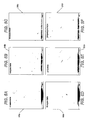
- Figures 4A-4F illustrate examples of n-type thermoelectric films epitaxially grown on GaAs substrates having several different crystal orientations evaluated in conjunction with substrates according to some embodiments of the present invention. More particularly, Figure 4A is an optical micrograph illustrating an n-type epitaxial film 410a grown on a GaAs substrate having a growth surface offcut from the (100) plane by about 2° toward the ⁇ 110> direction, also referred to hereinafter as the 2° film.
- Figure 4B is an optical micrograph illustrating an n-type epitaxial film 410b grown on a GaAs substrate having a growth surface offcut from the (100) plane by about 6° toward the ⁇ 110> direction, also referred to as the 6° film.
- Figure 4C is an optical micrograph illustrating an n-type epitaxial film 410c grown on a GaAs substrate having a growth surface offcut from the (100) plane by about 10° toward the ⁇ 110> direction, also referred to as the 10° film.
- Figure 4D is an optical micrograph illustrating an n-type epitaxial film 410d grown on a GaAs substrate having a growth surface offcut from the (100) plane by about 15° toward the ⁇ 110> direction, also referred to as the 15° film.
- Figure 4E is an optical micrograph illustrating an n-type epitaxial film 410e grown on a GaAs substrate having a growth surface parallel to the (111) plane (also referred to as the (111) film), and Figure 4F is an optical micrograph illustrating an n-type epitaxial film 410f grown on a GaAs substrate having a growth surface offcut from the (111) plane by about 2° toward the ⁇ 2-1-1> direction (also referred to as the (111) 2° film).
- the optical micrographs of Figures 4A-4F illustrate a film dimension of 2.2 mm x 2.2 mm.
- n-type films were grown initially, followed by x-ray diffraction, optical and electron microscopy, and Seebeck and Hall measurements. All films were grown using substantially similar growth conditions. As shown in Figures 4A-4F , surface defects are increased in the (111) film 410e of Figure 4E and in the 2° film 410a of Figure 4A relative to the other films 410b, 410c, 410d and 410f. Cracks are also evident in the 2° film 410a (about 6 cracks/mm) and in the (111) 2° film 410f (about 4 cracks/mm) via optical microscopy.
- the films 410b, 410c, and 410d of Figures 4B, 4C, and 4D grown on substrates offcut from the (100) plane by an offcut angle in the range of about 5° to about 30° toward the ⁇ 110> direction exhibited relatively fewer surface defects and almost no visible cracks (i.e., less than about 0.45 cracks/mm) than those of the films 410a and 410e. Additional growth experiments were conducted for thicker n-type and p-type films on the 15° off (100) toward ⁇ 110> surface, as discussed in greater detail below with reference to Figures 7 and 9 and Table 2.
- Figures 5A-5F illustrate scanning electron microscope (SEM) micrographs of n-type thermoelectric films epitaxially grown on GaAs substrates having several different crystal orientations evaluated in conjunction with substrates according to some embodiments of the present invention. More particularly, Figure 5A illustrates an n-type epitaxial film 510a grown on a GaAs substrate having a growth surface offcut from the (100) plane by about 2° toward the ⁇ 110> direction, also referred to hereinafter as the 2° film.
- Figure 5B illustrates an n-type epitaxial film 510b grown on a GaAs substrate having a growth surface offcut from the (100) plane by about 6° toward the ⁇ 110> direction, also referred to as the 6° film.
- Figure 5C illustrates an n-type epitaxial film 510c grown on a GaAs substrate having a growth surface offcut from the (100) plane by about 10° toward the ⁇ 110> direction, also referred to as the 10° film.
- Figure 5D illustrates an n-type epitaxial film 510d grown on a GaAs substrate having a growth surface offcut from the (100) plane by about 15° toward the ⁇ 110> direction, also referred to as the 15° film.
- Figure 5E illustrates an n-type epitaxial film 510e grown on a GaAs substrate having a growth surface parallel to the (111) plane (also referred to as the (111) film), and Figure 5F illustrates an n-type epitaxial film 510f grown on a GaAs substrate having a growth surface offcut from the (111) plane by about 2° toward the ⁇ 2-1-1> direction (also referred to as the (111) 2° film).
- the films 510b-510d grown on substrates offcut from the (100) plane by an offcut angle in the range of about 5° to about 30° toward the ⁇ 110> direction exhibited lower crack densities and fewer surface defects than those of the films 510a, 510e, and 510f.
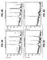
- Figures 6A-6F illustrates X-Ray Diffraction (XRD) of n-type thermoelectric films epitaxially grown on GaAs substrates having several different crystal orientations evaluated in conjunction with substrates according to some embodiments of the present invention. More particularly, Figure 6A illustrates x-ray diffraction of an n-type epitaxial film grown on a GaAs substrate having a growth surface offcut from the (100) plane by about 2° toward the ⁇ 110> direction, also referred to hereinafter as the 2° film.
- XRD X-Ray Diffraction
- Figure 6B illustrates x-ray diffraction of an n-type epitaxial film grown on a GaAs substrate having a growth surface offcut from the (100) plane by about 6° toward the ⁇ 110> direction, also referred to as the 6° film.
- Figure 6C illustrates x-ray diffraction of an n-type epitaxial film grown on a GaAs substrate having a growth surface offcut from the (100) plane by about 10° toward the ⁇ 110> direction, also referred to as the 10° film.
- Figure 6D illustrates x-ray diffraction of an n-type epitaxial film grown on a GaAs substrate having a growth surface offcut from the (100) plane by about 15° toward the ⁇ 110> direction, also referred to as the 15° film.
- Figure 6E illustrates x-ray diffraction of an n-type epitaxial film grown on a GaAs substrate having a growth surface parallel to the (111) plane (also referred to as the (111) film)
- Figure 6F illustrates x-ray diffraction of an n-type epitaxial film grown on a GaAs substrate having a growth surface offcut from the (111) plane by about 2° toward the ⁇ 2-1-1> direction (also referred to as the (111) 2° film).
- some other unidentified peaks 610e are observed, indicating a non-c-plane orientation.
- cracks are observed, the crystalline structure of the (111)2° film appears to be relatively good.
- Table 1 further illustrates the properties of the n-type thermoelectric films epitaxially grown on various GaAs substrates, as discussed above with reference to Figures 4A-4F , 5A-5F, and 6A-6F.
- the samples illustrated in Table 1 were grown using substantially similar growth conditions.
- Table 1 Sample Thickness ( ⁇ m) Rate ( ⁇ /min) Resist.
- thermoelectric films according to some embodiments of the present invention exhibited lower Seebeck coefficients, and thus, lower thermoelectric power factors (PF) than the 2°, (111), and/or (111) 2° films.
- the power factors for the 6°, 10°, and 15° thermoelectric films may be comparable to those of the 2°, (111), and/or (111) 2° films.
- thermoelectric films grown on substrates having growth surfaces that are offcut from the (100) plane by an offcut angle in the range of about 5° to about 30° according to some embodiments of the present invention may provide improved thermoelectric performance with reduced cracking.
- FIG. 7 illustrates film properties of a GaAs substrate according to some embodiments of the present invention.
- an SEM cross-section of a thermoelectric film 710 grown on a 15° off-axis (100) GaAs surface 700 is shown.
- the film 710 has a thickness 715 of approximately 4.4 ⁇ m.
- the c-plane lattice orientation of the film 710 is about 11.5° relative to the plane defined by the substrate surface 700.
- the c-plane lattice orientation of conventional epitaxial films grown on 2° off-axis (100) substrates may be about 1° relative to the plane defined by the substrate surface.
- thermoelectric films according to some embodiments of the present invention were observed to be approximately two times that of a conventional epitaxial film deposited on a 2° off-axis substrate.
- Figure 8 illustrates optical microscopy of a p-type thermoelectric film 810 epitaxially grown on a GaAs growth surface that is offcut 2° relative to the (100) plane toward the ⁇ 110> direction
- Figure 9 illustrates optical microscopy of a p-type thermoelectric film 910 according to some embodiments of the present invention epitaxially grown on a GaAs growth surface that is offcut 15° relative to the (100) plane toward the ⁇ 110> direction.
- the p-type films of Figures 8 and 9 were grown on the respective substrates to a thickness of approximately 6 ⁇ m.
- the p-type thermoelectric film 910 grown on the 15° off-axis substrate, as with the n-type films was substantially crack-free with relatively good surface morphology (i.e., few or no surface defects).
- Table 2 Film Type Thickness ( ⁇ m) Resist. ( ⁇ cm) Mobility (cm 2 /V-s) Carriers (cm -3 ) Seebeck ( ⁇ V/K) PF( ⁇ WK-2 cm-1) p-type 3.9 2.25E-03 219 1.27E+19 275 34 p-type 5.6 1.25E-03 254 1.96E+19 268 57 p-type 6.2 8.32E-04 299 2.51E+19 262 83 n-type 6.3 1.84E-03 252 1.35E+19 -347 65 n-type 10.8 1.71E-03 265 1.38E+19 -350 72
- FIGS 10A-10B illustrate methods of fabricating thermoelectric films on patterned substrates according to an embodiment of the present invention.
- a substrate 1000 is patterned and etched to define a plurality of mesas 1030 protruding from the surface 1005 of the substrate 1000.
- a mask pattern (not shown) may be formed on the surface 1005 of the substrate 1000, an etching process may be used to remove portions of the substrate 1000 not covered by the mask, and the mask pattern may be removed to define the mesas 1030.
- the mesas 1030 may be substantially circular in plan view, and may have a diameter of about 200 ⁇ m or less in some embodiments.
- the mesas 1030 may be elliptical or rectangular in plan view. In still other embodiments, the mesas 1030 may be elongated rectangles extending along the substrate 1000 to define "stripes" in plan view. The stripes may be oriented to be parallel to a direction in which cracks are typically formed. For instance, in n-type BiTe on (100) GaAs or other particular substrate, cracks may be known to form in a particular direction, and the mesas 1030 may be formed to run parallel to this direction with a spacing less than the nominal crack spacing. As such, when a thermoelectric film 1010 is epitaxially grown on the surface 1005 of the substrate 1000 as discussed below with reference to Figure 10B , substantially, crack free stripe-shaped thermoelectric film mesas 1020 may be produced.
- the surface 1005 of the substrate 1000 may be a vicinal growth surface that is offcut from a ⁇ 100 ⁇ plane, for example, as defined by the crystallographic orientation 1009 of the substrate 1000.
- the surface 1005 of the substrate 1000 may be offcut from the ⁇ 100 ⁇ plane toward a ⁇ 110> direction at an offcut angle of up to about 30 degrees. More particularly, as illustrated in detail in Figure 10A , the normal 1004 through the growth surface 1005 is tilted toward the [110] direction 1007 at an offcut angle ⁇ 1002 in the range of about 0° to about 45° off-axis from the [100] direction 1006.
- the offcut angle ⁇ 1002 may be about 5° to about 30°, and in some embodiments, about 10° to about 25°. In particular embodiments of the present invention, the offcut angle ⁇ 1002 may be about 15 degrees toward the ⁇ 110> direction relative to the (100) plane.
- thermoelectric (TE) film 1010 is epitaxially grown on the surface 1005 of the substrate 1000.
- the thermoelectric film 1010 may be a compound including Group V elements (such as bismuth (Bi) antimony (Sb), and/or lead (Pb)), and Group VI elements (such as tellurium (Te) and/or selenium (Se)).
- the thermoelectric film 1010 may be grown along its c-axis 1014 on the growth surface 1005 of the substrate 1000 in a substantially similar manner as described above with reference to Figures 3A-3B , and as such, further description thereof is omitted.
- thermoelectric film mesas 1020 may also be formed protruding from the growth surface 1005.
- the mesas 1020 may likewise be substantially circular, elliptical, or rectangular in plan view.
- substantially circular mesas 1020 may be similarly formed protruding from the growth surface 1005, and may similarly have a diameter of about 200 ⁇ m or less in some embodiments.
- the mesas 1030 in the substrate 1000 are substantially rectangular, the mesas 1020 may also be substantially rectangular, and may similarly extend parallel to a known direction in which cracks are typically formed in some embodiments.
- dimensions of the mesas 1020 may change and/or definition of the mesas 1020 may be reduced, for example, due to pattern washout.
- thermoelectric film 1010 may have a crystallographic orientation (indicated by hatched lines 1019) that is tilted by up to about 30 degrees relative to the plane defined by the surface 1005 and/or the plane defined by the surface 1025 of the film 1010 itself.
- the c-axis 1014 of the thermoelectric film 1010 is tilted off-axis from the normal 1004 to the surface 1005 by an angle ⁇ 1012 of about 0° to about 30°.
- the crystallographic tilt angle ⁇ 1012 of the thermoelectric film 1010 may be in the range of about 5° to about 30°.
- the crystallographic tilt angle ⁇ 1012 of the thermoelectric film 1010 may be about 10° to about 30°, and in particular embodiments, may be about 15° to about 25°.
- the portions of the thermoelectric film 1010 defined by the protruding surfaces of the mesas 1020 may be substantially crack-free depending on the size of the mesas 1020, as discussed below.
- thermoelectric films may include other methods for selective epitaxial growth of thermoelectric films on particular portions of the substrate.
- a mask pattern such as a silicon dioxide (SiO 2 ) mask, may be formed on the substrate 1000 to expose elliptical and/or rectangular portions of the substrate 1000. The mask pattern may prevent and/or inhibit growth in the masked regions.
- the "mesas" may not protrude from the substrate 1000, but rather, may generally refer to an unetched or unmasked area of the substrate 1000 on which a thermoelectric film may be epitaxially grown.
- a seed layer may be grown on the surface of the substrate prior to masking and/or etching the substrate for selective epitaxial growth of the thermoelectric film.
- a seed layer of BiTe or other Group V-Group VI alloy may be grown on the substrate 1000 prior to etching the substrate to provide the mesas 1030 protruding therefrom.
- Such a BiTe seed layer (or other Group V-Group VI alloy) may be grown on the substrate 1000 prior to forming a mask thereon that prevents and/or inhibits growth in the masked regions.
- the seed layer may help nucleate growth; the mask material may prevent direct growth, but may enable high-quality lateral growth in the plane of the substrate surface. Such lateral growth may or may not coalesce.
- the dimensions of the mask may be chosen so as to reduce, prevent, and/or minimize the incidence of cracks, and may vary depending on the substrate of choice.
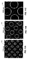
- FIGS 11A-11C are optical micrographs illustrating thermoelectric films epitaxially grown on different patterned substrates according to other embodiments of the present invention.
- substantially circular mesas 1120a-1120c were patterned and etched by reactive ion etching (RIE) into GaAs substrates having growth surfaces 2° off-axis of the (100) plane.
- Mesas of different diameters were etched to investigate variations in angle and size, and a 2.7 ⁇ m thick n-type film was grown on each wafer.
- Figure 11A illustrates results for a thermoelectric film grown on a GaAs substrate patterned with mesas 1120a having a diameter of about 150 ⁇ m.
- Figure 11B illustrates results for a thermoelectric film grown on a GaAs substrate patterned with mesas 1120b having a diameter of about 300 ⁇ m
- Figure 11C illustrates results for a thermoelectric film grown on a GaAs substrate patterned with mesas 1120c having a diameter of about 900 ⁇ m.
- relatively little cracking is observed in the 150 ⁇ m mesas 1120a.
- the 150 ⁇ m mesas 1120a may have a crack density of less than about 1 crack/mm, and in some embodiments, less than about 0.1 cracks/mm.
- some embodiments of the present invention may use thermoelectric films grown on substrates patterned with mesas having a diameter of about 200 ⁇ m or less.
- larger diameter mesas may be provided while maintaining a desired crack density.
- GaAs substrates having growth surfaces 6° or 15° off-axis of the (100) plane may be used to grow substantially crack-free mesas (e.g., less than about 1 crack/mm) having a diameter of less than about 400 ⁇ m, and in some embodiments, less than about 300 ⁇ m.
- the mesas may have widths corresponding to the diameters described above. Accordingly, some embodiments of the present invention may employ a combination of patterned substrates and substrates having increased offcut growth surfaces to provide thermoelectric films with reduced cracking.
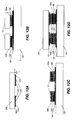
- thermoelectric element includes a structure having a layer of a thermoelectric film according to some embodiments of the present invention (such as Bi 2 Te 3 ) with a Seebeck coefficient sufficient to provide thermoelectric heat pumping (heating or cooling) responsive to an electrical current therethrough and/or electrical power generation responsive to a temperature gradient across the thermoelectric element.
- thermoelectric element may include one or more P-N couples with a P-N couple having a P-type thermoelectric element and an N-type thermoelectric element electrically coupled in series and thermally coupled in parallel and configured to provide thermoelectric heating, cooling, and/or power generation.
- thermoelectric material 1210 such as bismuth telluride or Bi 2 Te 3
- a sacrificial substrate 1200 such as a GaAs substrate
- the growth surface 1205 of the substrate 1200 may be offcut by an offcut angle ⁇ in the range of about 5 degrees to about 45 degrees relative to a ⁇ 100 ⁇ plane toward a ⁇ 110>, as discussed above, such that a crystallographic growth direction (indicated by hatched lines 1219) along the c-axis of the thin film thermoelectric material 1210 is not normal to the growth surface 1205 of the substrate 1200, but rather, is in the range of about 5 degrees to about 30 degrees off of the normal to the growth surface 1205.
- the thin film thermoelectric material 1210 has a crystallographic tilt angle ⁇ of about 5 degrees to about 30 degrees relative to a surface 1222 of the thermoelectric material 1210 adjacent to the offcut surface 1205 of the substrate 1200.
- the substrate 1200 is then patterned, cut, or otherwise formed to provide separate thermoelectric elements 1203.
- P-type and n-type thermoelectric elements may be separately formed on different substrates.
- a substrate with p-type thermoelectric elements may be diced to provide separate p-type thermoelectric elements, and a substrate with n-type thermoelectric elements may be diced to provide separate n-type thermoelectric elements. It is to be understood that the crystallographic tilt angle ⁇ need not be the same for n-type and p-type thermoelectric elements.
- a first header 1221 (such as a thermally conductive ceramic plate) includes a conductive metal trace 1207 thereon.
- a p-type thermoelectric element 1203a and an n-type thermoelectric element 1203b are bonded to the metal trace 1207, for example, using solder layers 1209. Portions 1201 of the sacrificial substrate(s) 1200 may be maintained on the thermoelectric elements 1203a and 1203b after bonding the respective thermoelectric elements 1203a and 1203b to the metal trace 207.
- thermoelectric elements 1203a and 1203b may also have a crystallographic tilt angle in the range of about 5 degrees to about 30 degrees relative to the header 1221.
- remaining portions of the sacrificial substrates 1201 may be removed, and metal contacts 1211 may be formed ( e.g ., electroplated) on the thermoelectric elements 1203a and 1203b.
- a second header 1231 with complementary traces 1217 may be bonded to the metal contacts 1211, for example, using solder layers 1215, as shown in Figure 12D .
- thermoelectric devices may include thermoelectric elements 1203a and 1203b that are fabricated in accordance with the methods described above with reference to Figures 3A-3B and/or Figures 10A-10B .
- the first header 1221 may be an integrated circuit (IC) semiconductor chip
- the second header 1231 may be a packaging substrate such as a printed circuit board substrate, a laminate carrier substrate, a chip carrier, a ball grid array substrate, a pin grid array substrate, a flip chip package substrate, a printed wire board, and/or any other substrate to which an integrated circuit chip or other electronic device may be bonded to provide a chip scale package.
- the integrated circuit semiconductor chip (as the first header 1221 ) may include an active side having electronic devices thereon adjacent the metal trace(s) 1207 and a backside opposite the active side.
- the second header 1231 may be an IC semiconductor chip, and the first header 1221 may be a packaging substrate.
- the P- and N-type thermoelectric elements 1203a and 1203b together define a P-N couple connected in series electrically, which may provide for either Peltier cooling and/or Seebeck power generation.
- the first header 1221 may be a substrate of a semiconductor electronic device or other structured to be heated/cold
- the second header 1231 may be a heat transfer structure such as a thermal mass, a heat sink, a heat spreader, a heat pipe, etc.
- thermoelectric cooling may be provided more directly adjacent heat generating circuitry on the active side of the IC semiconductor device without requiring heat transfer through the IC semiconductor device to a back side thereof.
- operations of forming the thermoelectric cooler may be integrated with operations of flip chip packaging.
- alignment of the thermoelectric cooler with a known hot spot on the active side of the IC semiconductor chip may be more easily facilitated than if thermoelectric cooling is provided on the backside of the IC semiconductor chip.
- the packaging substrate is thermally conductive, further modification thereof may not be required. If the packaging substrate is not thermally conductive (e.g.
- thermoelectric elements 1203 may be provided through the packaging substrate adjacent the thermoelectric elements 1203 to enhance thermal conduction through the packaging substrate.
- some embodiments of the present invention involve methods for depositing epitaxially grown thermoelectric films on GaAs substrates and related devices.
- a GaAs substrate is cut off-axis of the (100) plane toward the ⁇ 110> direction to define a growth surface at an offcut angle in the range of about 5 degrees to about 45 degrees.
- the offcut angle may be in the range of about 10 degrees to about 30 degrees.
- one of a number of offcut angles for the substrate surface may be used.
- the offcut angle may be about 15°.
- thermoelectric films having reduced cracking and/or substantially crack-free thermoelectric films may be epitaxially grown on the offcut growth surface.
- the methods described above may provide for an accelerated deposition rate as compared to a film grown on the (100) plane substrate cut at about 2° toward the ⁇ 110> direction.
- thermoelectric films may also be applied to reducing and/or eliminating out-of-plane surface defects in thermoelectric films formed on GaAs substrates.
- improved results may be observed with the GaAs substrate cut at about 15° off-axis of the (100) plane toward the ⁇ 110> direction.
- a signature of growing the substantially crack-free and/or reduced cracking thermoelectric epitaxial films on GaAs substrates that are cut off-axis of the (100) plane toward the ⁇ 110> direction is that the c-axis of the thermoelectric films is not normal to the growth surface of the GaAs substrate.
- the c-axis may be many different angles. In some embodiments, the c-axis may be in the range of about 5° to about 30° off of the normal to the GaAs growth surface, and in particular embodiments, may be about 10° to about 25° off-normal. For example, when the offcut angle of a GaAs growth surface is about 15°, the c-axis of the thermoelectric film may be about 11.5° off of the normal to the GaAs growth surface.
- Deposition of reduced cracking, substantially crack-free and/or semi crack-free thermoelectric films according to some embodiments of the present invention was also demonstrated on GaAs substrates patterned to define a plurality of protruding mesas.
- the mesas of GaAs may be generated, for example, by plasma etching into a GaAs wafer.
- the growth surface of the GaAs substrate may also be offcut from the (100) plane at an offcut angle of up to about 30° toward the ⁇ 110> direction.
- a GaAs growth surface having an offcut angle in the range of about 5° to about 30° may be patterned to define mesas having a diameter of about 150 ⁇ m or less for thermoelectric film growth.
- the protruding mesas may be substantially crack-free.
- thermoelectric films grown directly on offcut substrates and/or patterned substrates it is to be understood that, in some embodiments, one or more intermediate layers may be formed on the offcut and/or patterned substrates to facilitate high quality thermoelectric film growth thereon.
- a silicon (Si) substrate may be referred to as a non-polar material because it is not binary and does establish an orientation preference for binary or tertiary growth.
- thermoelectric film By introducing one or more layers of carbon (C), nitrogen (N), silicon carbide (SiC), and/or silicon nitride (SiN) on the growth substrate prior to the growth of the thermoelectric film, a relatively weak polarity can be established, and thus, improved thermoelectric films can be nucleated. Such an intermediate layer may also decrease, spread, and/or absorb the strain between the growth substrate and a relatively high lattice constant and/or thermally mismatched thermoelectric material. For instance, a layer with an intermediate lattice constant between a GaAs growth surface and a BiTe thermoelectric film could be deposited.
- Alloy layers of BiPbSbTeSe may also be used to bridge the mismatch, and may be graded to a provide a structure that has desired thermoelectric properties.
- Such an intermediate layer may also be sacrificial, and as such, may be removed with and/or after the substrate.
- Strained-layer superlattices may also be used as an intermediate layer to accommodate strain.
- AlAs/InAs and/or other superlattice technologies developed for the GaAs material system may be employed to manage the strain at the GaAs/thermoelectric film interface.
- a relatively pliable interlayer such as a relatively thin metallic layer, may be used to absorb some of the lattice strain.
Description
- The present application claims the benefit of priority from
U.S. Provisional Application No. 60/887,964 - The present invention relates to methods of fabricating thin film thermoelectric materials and related thermoelectric devices.
- Thermoelectric materials may be used to provide cooling and/or power generation according to the Peltier effect. Thermoelectric materials are discussed, for example, in the reference by Venkatasubramanian et al. entitled "Phonon-Blocking Electron-Transmitting Structures" (18th International Conference On Thermoelectrics, 1999).
- Application of solid state thermoelectric cooling may be expected to improve the performance of electronics and sensors such as, for example, RF receiver front-ends, infrared (IR) imagers, ultra-sensitive magnetic signature sensors, and/or superconducting electronics.
- The performance of a thermoelectric device may be a function of the figure(s)-of-merit (ZT) of the thermoelectric material(s) used in the device, with the figure-of-merit being given by:

where α, T, σ, KT are the Seebeck coefficient, absolute temperature, electrical conductivity, and total thermal conductivity, respectively. The material-coefficient Z can be expressed in terms of lattice thermal conductivity (KL), electronic thermal conductivity (Kc) and carrier mobility (µ), for a given carrier density (p) and the corresponding α, yielding equation (2) below:
where, L0 is the Lorenz number (approximately 1.5x10⁻⁸V2/K2 in non-degenerate semiconductors). State-of-the-art thermoelectric devices may use alloys, such as p-BixSb2-xTe3-ySey (x ≈≈ 0.5, y ≈≈ 0.12) and n-Bi2(SeyTe1-y)3 (y ≈≈ 0.05) for the 200 degree K to 400 degree K temperature range. For certain alloys, KL may be reduced more strongly than µ leading to enhanced ZT. - In addition, thin-film thermoelectric materials have been developed. For example, bismuth telluride (Bi2Te3) and/or antimony telluride (Sb2Te3)-based epitaxial films grown on gallium arsenide (GaAs) substrates may be used in the fabrication of thin-film thermoelectrics. However, the growth morphology of these films may be plagued by cracks and surface defects in the film. For example, a thermoelectric film grown on a 2° offcut GaAs substrate may have a crack density of about 5-20 cracks per millimeter (mm), and in some instances, greater than 10 cracks/mm. These cracks and defects may lead to reliability problems and/or complications in subsequent film processing, which may compromise one or more benefits that may be derived from the films.
- Accordingly, there continues to exist a need in the art for improved thermoelectric device fabrication methods and structures.
- Jung YC et al. (J. Crystal Growth, vol. 290, no. 2, pages 441-445, 2006) disclosed optimized growth parameters for good surface morphologies of Bi2Te3-based thermoelectric thin films for two-dimensional superlattice device applications.
- Asai H (J. Crystal Growth, vol. 80 (1987), pages 425-433) investigated metal organic chemical vapour deposition and found a fast lateral growth rate on {001} GaAs having round mesas. Asai also discloses a simple model for the lateral growth mechanism by consideration of atomic arrangements.
- Numus et al. (Eighteenth Int. Con. Thermoelectrics Proceedings, ICT'99, 1 January 1999, pages 696-699) discloses BiTe layers grown on {111} BaF2 substrates using a molecular beam technique.
- International patent application
WO 03/032408 A1 - Kim J-H et al. (Japanese Journal of Applied Physics, vol. 38, ) investigated metal organic vapour phase epitaxy for growth of Bi2Te3, and Sb2Te3 films on {001} GaAs substrates using trimethylbismuth, triethylantimony, ans diisopropyltelluride as metal organic sources. They identified growth parameters providing thin films with high Seebeck coefficients and atomistically smooth surface morphologies.
- In accordance with a first aspect of the present invention there is provided a method of fabricating a thermoelectric film on a growth substrate, the method comprising: patterning a substrate to define a growth surface having a plurality of mesas protruding therefrom, wherein the growth surface is offcut relative to a plane defined by a crystallographic orientation of the substrate at an offcut angle in a range from 10 degrees to 45 degrees; and then epitaxially growing a thermoelectric film on the growth surface wherein the thermoelectric film comprises a compound comprising bismuth (Bi), antimony (Sb), lead (Pb), tellurium (Te), and/or selenium (Se), and wherein the substrate comprises gallium arsenide (GaAs), silicon (Si), barium fluoride (BaF), silicon carbide (SiC), gallium nitride (GaN), aluminum nitride (AlN), sapphire, and/or glass.
- According to some embodiments, a method of fabricating a thermoelectric device includes providing a substrate including a growth surface that is offcut relative to a plane defined by a crystallographic orientation of the substrate at an offcut angle in a range of about 5 degrees to about 45 degrees. A thermoelectric film is epitaxially grown on the growth surface.
- In some embodiments, the plane defined by the crystallographic orientation of the substrate may be a {100} plane, and the growth surface may be a vicinal growth surface that is offcut from the {100} plane toward a <110> direction.
- In other embodiments, the offcut angle may be in a range of about 5 degrees to about 30 degrees, and in still other embodiments, in a range of about 10 degrees to about 20 degrees. For example, the offcut angle may be about 15 degrees relative to the {100} plane toward the <110> direction.
- In some embodiments, a crystallographic orientation of the thermoelectric film may be tilted at an angle in a range of about 5 degrees to about 30 degrees relative to the growth surface. For example, the crystallographic orientation of the thermoelectric film may be tilted at an angle in a range of about 10 degrees to about 25 degrees. More particularly, in some embodiments, the crystallographic orientation of the thermoelectric film may be tilted at an angle of about 11.5 degrees relative to the growth surface. In other embodiments, the crystallographic orientation of the thermoelectric film may be tilted at an angle in a range of about 18 degrees to about 24 degrees relative to the growth surface. For example, the crystallographic orientation of the thermoelectric film may be tilted at an angle of about 20 degrees relative to the growth surface. A plane defined by the crystallographic orientation of the thermoelectric film may be a (0015) plane.
- In other embodiments, the thermoelectric film may be a compound comprising bismuth (Bi), antimony (Sb), lead (Pb), tellurium (Te), and/or selenium (Se).
- In other embodiments, the substrate may be gallium arsenide (GaAs), silicon (Si), barium fluoride (BaF), silicon carbide (SiC), gallium nitride (GaN), aluminum nitride (AlN), sapphire, and/or glass.
- In some embodiments, the growth surface of the substrate may be patterned to define a plurality of mesas protruding therefrom prior to epitaxially growing the thermoelectric film. In some embodiments, a thermoelectric film seed layer may be epitaxially grown on the growth surface of the substrate prior to patterning the growth surface of the substrate.
- In other embodiments, prior to epitaxially growing the thermoelectric film, a mask pattern may be formed on the growth surface of the substrate to expose a plurality of portions thereof, and the thermoelectric film may be epitaxially grown on the plurality of exposed portions of the growth surface. In some embodiments, a thermoelectric film seed layer may be epitaxially grown on the growth surface prior to forming the mask pattern thereon.
- In some embodiments, at least one intermediate layer may be formed on the growth surface of the substrate prior to epitaxially growing the thermoelectric film thereon. The intermediate layer may include a silicon carbide (SiC) layer, an aluminum nitride (AlN) layer, a gallium arsenide (GaAs) layer, and/or a strained layer superlattice configured to help nucleation and/or accommodate strain between the growth surface and the thermoelectric film. For example, the intermediate layer may be a layer having a lattice constant between that of the substrate and the thermoelectric film, and in some embodiments, may be a graded layer configured to bridge a lattice mismatch between the substrate and the thermoelectric film.
- In other embodiments, the thermoelectric film may be epitaxially grown to a thickness in a range of about 5 micrometers (µm) to about 100 µm. For example, the thermoelectric film may be grown to a thickness of about 40 µm or less. The thermoelectric film may have a crack density of less than about 1 crack per millimeter (mm), and in some embodiments, less than about I crack per centimeter (cm).
- According to further embodiments, a method of fabricating a thermoelectric device includes patterning a substrate to define a growth surface having a plurality of mesas protruding therefrom. A thermoelectric film is epitaxially grown on the growth surface.
- In some embodiments, the thermoelectric film may be epitaxially grown to include a plurality of mesas protruding from the growth surface. The plurality of mesas of the thermoelectric film may be substantially elliptical or rectangular in plan view.
- In some embodiments, the plurality of mesas of the thermoelectric film may be elongated rectangular mesas extending in a direction substantially parallel to at least one crack in the thermoelectric film.
- In other embodiments, the plurality of mesas of the thermoelectric film may have a diameter or width of about 200 micrometers (µm) or less.
- In some embodiments, a mesa of the thermoelectric film may have a crack density of less than about 1 crack per millimeter (mm).
- In other embodiments, a crystallographic orientation of the thermoelectric film may be tilted at an angle in a range of about 5 degrees to about 30 degrees relative to the growth surface. The plurality of mesas of the thermoelectric film may have a diameter or width of about 400 micrometers (µm) or less, and in some embodiments, about 300µm or less.
- In other embodiments, the substrate may be a vicinal growth surface that is offcut relative to a plane defined by a crystallographic orientation of the substrate at an offcut angle in a range of about 5 degrees to about 45 degrees. For example, the plane defined by the crystallographic orientation of the substrate may be a {100} plane, and the vicinal growth surface may be offcut from the {100} plane toward a <110> direction. Also, the offcut angle may be in a range of about 5 degrees to about 30 degrees.
- In some embodiments, a thermoelectric film seed layer may be epitaxially grown on the substrate prior to patterning the substrate.
- According to still other embodiments, the thermoelectric film includes a thermoelectric material layer having a thickness of less than about 100 micrometers (µm) and a crack density of less than about 1 crack per millimeter (mm).
- In some embodiments, a crystallographic orientation of the thermoelectric material layer may be tilted at an angle in a range of about 5 degrees to about 30 degrees relative to a surface of the thermoelectric material layer. A plane defined by the crystallographic orientation of the thermoelectric material layer may be a (0015) plane.
- In other embodiments, the thermoelectric material layer may have a thickness in a range of about 5 micrometers (µm) to about 100 µm. The thermoelectric material layer may be a compound comprising bismuth (Bi), antimony (Sb), lead (Pb), tellurium (Te), and/or selenium (Se).
-
Figure 1 is a focused ion beam cross-sectional image illustrating an epitaxially grown thermoelectric film. -
Figure 2 is an optical micrograph illustrating cracks and surface defects in an epitaxially grown thermoelectric film. -
Figures 3A-3B are cross-sectional views illustrating methods of fabricating thermoelectric films on offcut substrates. -
Figures 4A-4F are optical micrographs illustrating n-type thermoelectric films epitaxially grown on gallium arsenide substrates of different crystal orientations including substrates. -
Figures 5A-5F are scanning electron microscope (SEM) micrographs illustrating n-type thermoelectric films epitaxially grown on gallium arsenide substrates of different crystal orientations including substrates. -
Figures 6A-6F are graphs illustrating x-ray diffraction (XRD) of n-type thermoelectric films epitaxially grown on gallium arsenide substrates of different crystal orientations including substrates. -
Figure 7 is a cross-sectional view illustrating a thermoelectric film grown on a gallium arsenide substrate . -
Figure 8 is an optical micrograph illustrating a thermoelectric film epitaxially grown on a gallium arsenide substrate. -
Figure 9 is an optical micrograph illustrating a thermoelectric film epitaxially grown on a gallium arsenide substrate. -
Figures 10A-10B are cross-sectional views illustrating methods of fabricating thermoelectric films on patterned substrates according to an embodiment of the present invention. -
Figures 11A-11C are optical micrographs illustrating thermoelectric films epitaxially grown on different patterned substrates according to an embodiment of the present invention. -
Figures 12A-12D are cross-sectional view illustrating methods of fabricating thermoelectric devices including thermoelectric films epitaxially grown on substrates according to some embodiments of the present invention. - The present invention is described more fully hereinafter with reference to the accompanying drawings, in which embodiments of the present invention are shown. In the drawings, the sizes and relative sizes of layers and regions may be exaggerated for clarity. Like numbers refer to like elements throughout.
- It will be understood that when an element or layer is referred to as being "on", "connected to" or "coupled to" another element or layer, it can be directly on, connected or coupled to the other element, or layer or intervening elements or layers may be present. In contrast, when an element is referred to as being "directly on," "directly connected to" or "directly coupled to" another element or layer, there are no intervening elements or layers present. As used herein, the term "and/or" includes any and all combinations of one or more of the associated listed items.
- It will be understood that, although the terms first, second, third etc. may be used herein to describe various elements, components, regions, layers and/or sections, these elements, components, regions, layers and/or sections should not be limited by these terms. These terms are only used to distinguish one element, component, region, layer or section from another region, layer or section. Thus, a first element, component, region, layer or section discussed below could be termed a second element, component, region, layer or section without departing from the teachings of the present invention.
- Spatially relative terms, such as "beneath", "below", "lower", "above", "upper" and the like, may be used herein for ease of description to describe one element or feature's relationship to another element(s) or feature(s) as illustrated in the figures. It will be understood that the spatially relative terms are intended to encompass different orientations of the device in use or operation in addition to the orientation depicted in the figures. For example, if the device in the figures is turned over, elements described as "below" or "beneath" other elements or features would then be oriented "above" the other elements or features. Thus, the exemplary term "below" can encompass both an orientation of above and below. The device may be otherwise oriented (rotated 90 degrees or at other orientations) and the spatially relative descriptors used herein interpreted accordingly. Also, as used herein, "lateral" refers to a direction that is substantially orthogonal to a vertical direction.
- The terminology used herein is for the purpose of describing particular embodiments only, and is not intended to be limiting of the present invention. As used herein, the singular forms "a", "an" and "the" are intended to include the plural forms as well, unless the context clearly indicates otherwise. It will be further understood that the terms "comprises" and/or "comprising," when used in this specification, specify the presence of stated features, integers, steps, operations, elements, and/or components, but do not preclude the presence or addition of one or more other features, integers, steps, operations, elements, components, and/or groups thereof.
- Example embodiments of the present invention are described herein with reference to cross-section illustrations that are schematic illustrations of idealized embodiments (and intermediate structures) of the invention. As such, variations from the shapes of the illustrations as a result, for example, of manufacturing techniques and/or tolerances, are to be expected. Thus, embodiments of the present invention should not be construed as limited to the particular shapes of regions illustrated herein but are to include deviations in shapes that result, for example, from manufacturing. For example, an implanted region illustrated as a rectangle will, typically, have rounded or curved features and/or a gradient of implant concentration at its edges rather than a binary change from implanted to non-implanted region. Likewise, a buried region formed by implantation may result in some implantation in the region between the buried region and the surface through which the implantation takes place. Thus, the regions illustrated in the figures are schematic in nature and their shapes are not intended to illustrate the actual shape of a region of a device and are not intended to limit the scope of the present invention.
- Unless otherwise defined, all terms (including technical and scientific terms) used herein have the same meaning as commonly understood by one of ordinary skill in the art to which this invention belongs. Accordingly, these terms can include equivalent terms that are created after such time. It will be further understood that terms, such as those defined in commonly used dictionaries, should be interpreted as having a meaning that is consistent with their meaning in the present specification and in the context of the relevant art, and will not be interpreted in an idealized or overly formal sense unless expressly so defined herein. All publications, patent applications, patents, and other references mentioned herein are incorporated by reference in their entirety.
- While some embodiments are described below with reference to metal organic chemical vapor deposition (MOCVD), it is to be understood that other methods of thermoelectric film deposition may also be used in embodiments of the present invention. For instance, molecular beam epitaxy (MBE), thermal or e-beam evaporation, sputtering, vapor phase epitaxy, alternate layer epitaxy, laser ablation, and/or other techniques used for thin film crystal growth may be used.
- Crystallographic oreintation in thermoelectric films and/or growth substrates according to some embodiments of the present invention is described herein with reference to Miller indicies. As used herein, Miller indicies in square brackets, such as [100], denote a direction, while Miller indicies in angle brackets or chevrons, such as <100>, denote a family of directions that are equivalent due to crystal symmetry. For example, in a cubic system, <100> refers to the [100], [010], [001] directions and/or the negative of any of these directions, noted as the [-100], [0-10], [00-1] directions. Miller indices in parentheses, such as (100), denote a plane. In a cubic system, the normal to the (100) plane is the direction [100]. Miller indicies in curly brackets or braces, such as {100}, denote a family of planes that are equivalent due to crystal symmetry, in a manner similar to the way angle brackets denote a family of directions.
-
Figures 1 and 2 illustrate examples of cracks and surface defects that may occur in epitaxial thin film thermoelectric materials. As shown in cross section inFigure 1 , acrack 101 extends through a bismuth antimony telluride selenium (BiSbTeSe)-basedepitaxial film 105 on a gallium arsenide (GaAs)substrate 100.Figure 2 further illustratescracks 201 andsurface defects 202 in a BiSbTeSe-based epitaxial film 205. Possible explanations for the cracking in thefilms 105 and/or 205 illustrated inFigures 1 and 2 may include poor lattice matching between the GaAs substrate and the BiSbTeSe-based epitaxial films, and/or a coefficient of thermal expansion (CTE) mismatch between the GaAs substrate and the BiSbTeSe-based epitaxial films. - A barium fluoride (BaF) substrate may be a good candidate for BiSbTeSe-based epitaxial films because it may provide good CTE and lattice matching. A silicon (Si) substrate may also be a good candidate for BiSbTeSe-based epitaxial films because they are available at low cost and relatively large sizes. However, sapphire, silicon carbide (SiC), gallium nitride (GaN), aluminum nitride (A1N), glass, and/or other substrates that provide an adequate seed for growth of a thermoelectric film may also be used. Interlayers such as silicon carbide (SiC), aluminum nitride (A1N), GaAs, and/or strained layer superlattices may also be formed on the substrate to help growth nucleation and/or to accommodate strain.
- Some embodiments consider the effects of two parameters on the density of cracking in thermoelectric films, such as BiSbTeSe-based films, epitaxially grown on a GaAs substrate: (1) GaAs crystal orientation; and (2) patterning of GaAs prior to epitaxy.
-
Figures 3A and 3B illustrate methods of fabricating a thermoelectric film on a growth substrate. Referring now toFigure 3A , asubstrate 300 is provided including agrowth surface 305. For instance, thesubstrate 300 may be a gallium arsenide (GaAs), silicon (Si), barium fluoride (BaF), sapphire, silicon carbide (SiC), gallium nitride (GaN), aluminum nitride (A1N), and/or glass substrate. Thegrowth surface 305 is offcut relative to a plane defined by the crystallographic orientation (indicated by hatched lines 309) of thesubstrate 300. As used herein, the term "offcut" refers to a miscut, misorientation, and/or tilt of a substrate surface relative to another surface or plane. For example, where thesubstrate 300 is a GaAs substrate having a cubic crystal structure, thegrowth surface 305 may be offcut relative to thecrystallographic orientation 309 of thesubstrate 300 along the (100) plane. Also, as described herein, the direction of a surface or plane is defined by a direction that is normal or perpendicular to the surface or plane. As such, an "offcut" or "vicinal" surface also describes a surface having a normal that is off-axis or tilted relative to the normal of the particular surface or plane. Accordingly, for a GaAs substrate, the normal 304 to thegrowth surface 305 may be off-axis relative to thedirection 306 of the (100) plane, i.e., the [100] direction. - Offcut wafers in accordance with embodiments of the present invention can be produced by different methods. For instance, a long GaAs boule can be oriented and sliced to produce wafer surfaces with an offcut angle relative to the GaAs lattice c-plane. Vicinal GaAs can also be grown on a vicinal template that is removed after deposition of the vicinal GaAs material, to yield a freestanding vicinal GaAs substrate. Other techniques for providing the
offcut growth surface 305 are well-known to those of ordinary skill in the art and will not be described further herein. - Still referring to
Figure 3A , thegrowth surface 305 of thesubstrate 300 according to some embodiments of the present invention is a vicinal surface offcut from a {100} plane toward a <110> direction at an angle θ (hereinafter referred to as an "offcut angle" 302) in the range of about 5 degrees (°) to about 45 degrees. For example, in some embodiments, theoffcut angle 302 of thegrowth surface 305 relative to the (100) plane may be in the range of about 10 degrees to about 30 degrees. More particularly, theoffcut angle 302 may be about 15 degrees toward the <110> direction. Such agrowth surface 305 is also referred to herein as a 15° off (100) surface. Accordingly, as shown inFigure 3A , the normal 304 through thegrowth surface 305 is tilted off-axis from the [100]direction 306 toward the [110]direction 307 at anoffcut angle 302 of about 5° to about 30°. The use of an intentionallyoffcut growth surface 305 provides atomic step edges and/or kinks (not shown) along thegrowth surface 305 that serve as preferential nucleation sites for the growth of athermoelectric layer 310 thereon, as shown inFigure 3 B. The selection of theoffcut angle 302 may define the lateral periodicity of the steps at thegrowth surface 305, as the offcut angle of a vicinal surface may determine the average spacing between steps. - Referring now to
Figure 3B , a thermoelectric (TE)film 310 is epitaxially grown on thegrowth surface 305 of thesubstrate 300. Thethermoelectric film 310 may be a compound including Group V elements (such as bismuth (Bi) antimony (Sb), and/or lead (Pb)), and Group VI elements (such as tellurium (Te) and/or selenium (Se)). For example, in some embodiments, thethermoelectric film 310 may be an epitaxial film of Bi2Te3 grown by metal organic chemical vapor deposition (MOCVD) on a GaAs substrate carried out in a reactor at a growth temperature of about 350° C and a growth pressure of about 350 Torr by the pyrolytic reaction of trimethylbismuth (TMBi) and diisopropyltelluride (DiPTe). Techniques for such epitaxial growth are further described, for example, in the publications by Venkatasubramanian et al. "MOCVD of Bi2Te3 and/or Sb2Te3 and their superlattice structures for thin-film thermoelectric applications", (Journal of Crystal Growth 170, 1997), and " Low-temperature organometallic epitaxy and its application to superlattice structures in thermoelectrics" (Applied Physics Letters Vol. 75, No. 8, 1999). Thethermoelectric film 310 may include a single alloy layer, multiple layers, and/or graded layers, and may be grown using steady gas flows, alternating flows, pauses, etc. using ones of the above-described Group V and/or Group VI elements. - Still referring to
Figure 3B , due to the offcut of thegrowth surface 305, the crystallographic direction of thethermoelectric film 310 along the c-axis 314 is not perpendicular to thegrowth surface 305. More particularly, the c-plane of thethermoelectric film 310 has a crystallographic orientation (indicated by hatched lines 319) that is tilted by about 5 degrees to about 30 degrees relative to the plane defined by thegrowth surface 305 and/or the plane defined by thesurface 325 of thefilm 310 itself. Thus, as illustrated inFigure 3B , the c-axis 314 of thethermoelectric film 310 is tilted off-axis from the normal 304 to thegrowth surface 305 by anangle ϕ 312 in the range of about 5° to about 30°. For example, theangle ϕ 312 may be in the range of about 10° to about 25°, and more specifically, about 18° to about 24°. In some embodiments, thecrystallographic orientation 319 of thethermoelectric film 310 may be tilted at anangle ϕ 312 of about 11.5 degrees relative to the plane of thegrowth surface 305; thus, the c-axis 314 of thefilm 310 may be about 11.5° off of the normal 304. In other embodiments, thecrystallographic orientation 319 may be tilted at anangle ϕ 312 of about 20 degrees relative to the plane of thegrowth surface 305. Accordingly, theoffcut angle 302 of thegrowth surface 305 may influence thecrystallographic tilt angle 312 of thethermoelectric film 310 grown on thegrowth surface 305. Theoffcut angle 302 of thegrowth surface 305 may be greater than thecrystallographic tilt angle 312 of thethermoelectric film 310 grown thereon in some embodiments; however, in other embodiments, theoffcut angle 302 may be less than or equal to thecrystallographic tilt angle 312. - The
thermoelectric film 310 may be grown to a thickness of about 5 micrometers (µm) to about 100 µm. For example, in some embodiments, thethermoelectric film 310 may have a thickness of about 40 µm or less. In addition, thermoelectric films epitaxially grown on substrates according to some embodiments of the present invention may have a reduced incidence of cracks and/or surface defects than thermoelectric films grown on conventional substrates, such as substrates having a growth surface that is offcut relative to a {100} plane at an offcut angle of about 2 degrees. For example, in some embodiments, thethermoelectric film 310 may have a crack density of less than about 1 crack per millimeter (mm). As used herein, the terms "crack density" or "cracks/mm" refer to a linear measurement based on the number of cracks in a thermoelectric film that intersect with a line of a predetermined length drawn across the thermoelectric film, divided by the length of the line. - Although described in
Figures 3A-3B primarily with reference to offcut angles varying from about 5 degrees to about 30 degrees, other substrate materials, substrate orientations, offcut angles, and offcut directions may be used without differing from the scope of the present invention. Further, due to manufacturing tolerances, a substrate prepared based on an offcut angle and/or direction according to some embodiments of the present invention may vary by small amounts relative to the intended offcut angle and direction. In other words, offcut angles and directions described herein refer to intended values, and small differences are assumed without departing from the scope of the present invention. In addition, due to manufacturing tolerances, the deposition of thermoelectric layers may invariably occur on a vicinal surface. Accordingly, the scope of the present invention includes the deposition of thermoelectric layers where the offcut of the substrate is intentionally controlled to result in improved material and/or device properties. -
Figures 4A-4F illustrate examples of n-type thermoelectric films epitaxially grown on GaAs substrates having several different crystal orientations evaluated in conjunction with substrates according to some embodiments of the present invention. More particularly,Figure 4A is an optical micrograph illustrating an n-type epitaxial film 410a grown on a GaAs substrate having a growth surface offcut from the (100) plane by about 2° toward the <110> direction, also referred to hereinafter as the 2° film.Figure 4B is an optical micrograph illustrating an n-type epitaxial film 410b grown on a GaAs substrate having a growth surface offcut from the (100) plane by about 6° toward the <110> direction, also referred to as the 6° film.Figure 4C is an optical micrograph illustrating an n-type epitaxial film 410c grown on a GaAs substrate having a growth surface offcut from the (100) plane by about 10° toward the <110> direction, also referred to as the 10° film.Figure 4D is an optical micrograph illustrating an n-type epitaxial film 410d grown on a GaAs substrate having a growth surface offcut from the (100) plane by about 15° toward the <110> direction, also referred to as the 15° film.Figure 4E is an optical micrograph illustrating an n-type epitaxial film 410e grown on a GaAs substrate having a growth surface parallel to the (111) plane (also referred to as the (111) film), andFigure 4F is an optical micrograph illustrating an n-type epitaxial film 410f grown on a GaAs substrate having a growth surface offcut from the (111) plane by about 2° toward the <2-1-1> direction (also referred to as the (111) 2° film). The optical micrographs ofFigures 4A-4F illustrate a film dimension of 2.2 mm x 2.2 mm. - In the embodiments of
Figures 4A-4F ,2-4 µm thick n-type films were grown initially, followed by x-ray diffraction, optical and electron microscopy, and Seebeck and Hall measurements. All films were grown using substantially similar growth conditions. As shown inFigures 4A-4F , surface defects are increased in the (111)film 410e ofFigure 4E and in the 2°film 410a ofFigure 4A relative to theother films film 410a (about 6 cracks/mm) and in the (111) 2°film 410f (about 4 cracks/mm) via optical microscopy. As such, thefilms Figures 4B, 4C, and 4D grown on substrates offcut from the (100) plane by an offcut angle in the range of about 5° to about 30° toward the <110> direction exhibited relatively fewer surface defects and almost no visible cracks (i.e., less than about 0.45 cracks/mm) than those of thefilms Figures 7 and9 and Table 2. -
Figures 5A-5F illustrate scanning electron microscope (SEM) micrographs of n-type thermoelectric films epitaxially grown on GaAs substrates having several different crystal orientations evaluated in conjunction with substrates according to some embodiments of the present invention. More particularly,Figure 5A illustrates an n-type epitaxial film 510a grown on a GaAs substrate having a growth surface offcut from the (100) plane by about 2° toward the <110> direction, also referred to hereinafter as the 2° film.Figure 5B illustrates an n-type epitaxial film 510b grown on a GaAs substrate having a growth surface offcut from the (100) plane by about 6° toward the <110> direction, also referred to as the 6° film.Figure 5C illustrates an n-type epitaxial film 510c grown on a GaAs substrate having a growth surface offcut from the (100) plane by about 10° toward the <110> direction, also referred to as the 10° film.Figure 5D illustrates an n-type epitaxial film 510d grown on a GaAs substrate having a growth surface offcut from the (100) plane by about 15° toward the <110> direction, also referred to as the 15° film.Figure 5E illustrates an n-type epitaxial film 510e grown on a GaAs substrate having a growth surface parallel to the (111) plane (also referred to as the (111) film), andFigure 5F illustrates an n-type epitaxial film 510f grown on a GaAs substrate having a growth surface offcut from the (111) plane by about 2° toward the <2-1-1> direction (also referred to as the (111) 2° film). - As shown in the SEM micrographs of
Figures 5A-5F , surface defects are evident in the 2°film 510a, the (111)film 510e, and the (111) 2°film 510f. However, fewer surface defects are evident in the 6°film 510b, the 10°film 510c, and the 15°film 510d. Cracks are also evident in the 2°film 510a (about 16 cracks/mm) and the (111) 2°film 510f (about 10 cracks/mm). However, as shown inFigure 5D , reduced cracking is provided in the 15°film 510d, as well as in the 6°film 510b ofFigure 5B , relative to theother films films 510b-510d grown on substrates offcut from the (100) plane by an offcut angle in the range of about 5° to about 30° toward the <110> direction exhibited lower crack densities and fewer surface defects than those of thefilms -
Figures 6A-6F illustrates X-Ray Diffraction (XRD) of n-type thermoelectric films epitaxially grown on GaAs substrates having several different crystal orientations evaluated in conjunction with substrates according to some embodiments of the present invention. More particularly,Figure 6A illustrates x-ray diffraction of an n-type epitaxial film grown on a GaAs substrate having a growth surface offcut from the (100) plane by about 2° toward the <110> direction, also referred to hereinafter as the 2° film.Figure 6B illustrates x-ray diffraction of an n-type epitaxial film grown on a GaAs substrate having a growth surface offcut from the (100) plane by about 6° toward the <110> direction, also referred to as the 6° film.Figure 6C illustrates x-ray diffraction of an n-type epitaxial film grown on a GaAs substrate having a growth surface offcut from the (100) plane by about 10° toward the <110> direction, also referred to as the 10° film.Figure 6D illustrates x-ray diffraction of an n-type epitaxial film grown on a GaAs substrate having a growth surface offcut from the (100) plane by about 15° toward the <110> direction, also referred to as the 15° film.Figure 6E illustrates x-ray diffraction of an n-type epitaxial film grown on a GaAs substrate having a growth surface parallel to the (111) plane (also referred to as the (111) film), andFigure 6F illustrates x-ray diffraction of an n-type epitaxial film grown on a GaAs substrate having a growth surface offcut from the (111) plane by about 2° toward the <2-1-1> direction (also referred to as the (111) 2° film). - As shown in
Figure 6A-6D , in films deposited on (100) vicinal GaAs, the primary Bi2Te3 peak (0015) is observed at approximately 45° 2Θ. Other major observable peaks are associated with the GaAs substrate or the (00ℓ) reflections of Bi2Te3, where t = 9, 12, 15, 18, 21, and 24, indicating growth of the films along the crystallographic c-axis. - As further shown in
Figures 6E-6F , thepeaks 610f observed on the (111) 2° film are (00ℓ), where t = 9, 12, 15, 18, 21, and 24. For the case of the (111) film, some otherunidentified peaks 610e are observed, indicating a non-c-plane orientation. Although cracks are observed, the crystalline structure of the (111)2° film appears to be relatively good. - Table 1 further illustrates the properties of the n-type thermoelectric films epitaxially grown on various GaAs substrates, as discussed above with reference to
Figures 4A-4F ,5A-5F, and6A-6F. The samples illustrated in Table 1 were grown using substantially similar growth conditions.Table 1 Sample Thickness (µm) Rate (Å/min) Resist. (Ω cm) Mobility (cm2/V-s) Carriers (cm-3) Seebeck (µV/K) PF(µW K-2 cm-1) 2° film 2.5 188 2.38E-03 178 1.48E+19 -371 58 6° film 3.1 238 2.11E-03 220 1.34E+19 -304 44 10° film 4.2 329 3.41E-03 185 9.91E+18 -287 24 15° film 4.4 346 2.87E-03 191 1.41E+19 -278 27 (111) film 1.1 71 1.06E-03 215 2.74E+19 -329 102 (111) 2° film 2.2 163 1.76E-03 188 1.88E+19 -318 57 - As shown in Table 1, the 6°, 10°, and 15° thermoelectric films according to some embodiments of the present invention exhibited lower Seebeck coefficients, and thus, lower thermoelectric power factors (PF) than the 2°, (111), and/or (111) 2° films. However, it should be noted that, when conditions are improved and/or optimized for substrates having growth surfaces that are offcut according to some embodiments of the present invention, the power factors for the 6°, 10°, and 15° thermoelectric films may be comparable to those of the 2°, (111), and/or (111) 2° films. Thus, thermoelectric films grown on substrates having growth surfaces that are offcut from the (100) plane by an offcut angle in the range of about 5° to about 30° according to some embodiments of the present invention may provide improved thermoelectric performance with reduced cracking.
-
Figure 7 illustrates film properties of a GaAs substrate according to some embodiments of the present invention. Referring now toFigure 7 , an SEM cross-section of athermoelectric film 710 grown on a 15° off-axis (100)GaAs surface 700 is shown. Thefilm 710 has athickness 715 of approximately 4.4 µm. Based on x-ray diffraction measurements, the c-plane lattice orientation of thefilm 710 is about 11.5° relative to the plane defined by thesubstrate surface 700. In contrast, the c-plane lattice orientation of conventional epitaxial films grown on 2° off-axis (100) substrates may be about 1° relative to the plane defined by the substrate surface. Also, growth rates increased as the offcut angle of thesubstrate surface 700 was increased, for example, due to an increased number of nucleation kink sites. Subsequent n-type film depositions were also conducted on the 15° off-axis substrate according to some embodiments of the present invention. Films of 6 µm and 10.8 µm without significant cracks were observed. The deposition rates of thermoelectric films according to some embodiments of the present invention were observed to be approximately two times that of a conventional epitaxial film deposited on a 2° off-axis substrate. -
Figure 8 illustrates optical microscopy of a p-typethermoelectric film 810 epitaxially grown on a GaAs growth surface that is offcut 2° relative to the (100) plane toward the <110> direction, whileFigure 9 illustrates optical microscopy of a p-typethermoelectric film 910 according to some embodiments of the present invention epitaxially grown on a GaAs growth surface that is offcut 15° relative to the (100) plane toward the <110> direction. The p-type films ofFigures 8 and 9 were grown on the respective substrates to a thickness of approximately 6 µm. As shown inFigure 9 , the p-typethermoelectric film 910 grown on the 15° off-axis substrate, as with the n-type films, was substantially crack-free with relatively good surface morphology (i.e., few or no surface defects). - Measured Hall and Seebeck data for the above p-type and n-type thermoelectric films grown on 15° offcut GaAs toward the <110> direction is provided below in Table 2.
Table 2 Film Type Thickness (µm) Resist. (Ω cm) Mobility (cm2/V-s) Carriers (cm-3) Seebeck (µV/K) PF(µWK-2 cm-1) p-type 3.9 2.25E-03 219 1.27E+19 275 34 p-type 5.6 1.25E-03 254 1.96E+19 268 57 p-type 6.2 8.32E-04 299 2.51E+19 262 83 n-type 6.3 1.84E-03 252 1.35E+19 -347 65 n-type 10.8 1.71E-03 265 1.38E+19 -350 72 -
Figures 10A-10B illustrate methods of fabricating thermoelectric films on patterned substrates according to an embodiment of the present invention. Referring now toFigure 10A , asubstrate 1000 is patterned and etched to define a plurality ofmesas 1030 protruding from thesurface 1005 of thesubstrate 1000. For example, a mask pattern (not shown) may be formed on thesurface 1005 of thesubstrate 1000, an etching process may be used to remove portions of thesubstrate 1000 not covered by the mask, and the mask pattern may be removed to define themesas 1030. Themesas 1030 may be substantially circular in plan view, and may have a diameter of about 200µm or less in some embodiments. However, in other embodiments, themesas 1030 may be elliptical or rectangular in plan view. In still other embodiments, themesas 1030 may be elongated rectangles extending along thesubstrate 1000 to define "stripes" in plan view. The stripes may be oriented to be parallel to a direction in which cracks are typically formed. For instance, in n-type BiTe on (100) GaAs or other particular substrate, cracks may be known to form in a particular direction, and themesas 1030 may be formed to run parallel to this direction with a spacing less than the nominal crack spacing. As such, when athermoelectric film 1010 is epitaxially grown on thesurface 1005 of thesubstrate 1000 as discussed below with reference toFigure 10B , substantially, crack free stripe-shapedthermoelectric film mesas 1020 may be produced. - In some embodiments, the
surface 1005 of thesubstrate 1000 may be a vicinal growth surface that is offcut from a {100} plane, for example, as defined by thecrystallographic orientation 1009 of thesubstrate 1000. Thesurface 1005 of thesubstrate 1000 may be offcut from the {100} plane toward a <110> direction at an offcut angle of up to about 30 degrees. More particularly, as illustrated in detail inFigure 10A , the normal 1004 through thegrowth surface 1005 is tilted toward the [110]direction 1007 at an offcut angle θ 1002 in the range of about 0° to about 45° off-axis from the [100]direction 1006. For example, the offcut angle θ 1002 may be about 5° to about 30°, and in some embodiments, about 10° to about 25°. In particular embodiments of the present invention, the offcut angle θ 1002 may be about 15 degrees toward the <110> direction relative to the (100) plane. - Referring now to
Figure 10B , a thermoelectric (TE)film 1010 is epitaxially grown on thesurface 1005 of thesubstrate 1000. Thethermoelectric film 1010 may be a compound including Group V elements (such as bismuth (Bi) antimony (Sb), and/or lead (Pb)), and Group VI elements (such as tellurium (Te) and/or selenium (Se)). Thethermoelectric film 1010 may be grown along its c-axis 1014 on thegrowth surface 1005 of thesubstrate 1000 in a substantially similar manner as described above with reference toFigures 3A-3B , and as such, further description thereof is omitted. Due to patterning of thesubstrate 1000 described above with reference toFigure 10A prior to growth of thefilm 1010,thermoelectric film mesas 1020 may also be formed protruding from thegrowth surface 1005. Themesas 1020 may likewise be substantially circular, elliptical, or rectangular in plan view. For example, where themesas 1030 in thesubstrate 1000 are substantially circular, substantiallycircular mesas 1020 may be similarly formed protruding from thegrowth surface 1005, and may similarly have a diameter of about 200 µm or less in some embodiments. Likewise, where themesas 1030 in thesubstrate 1000 are substantially rectangular, themesas 1020 may also be substantially rectangular, and may similarly extend parallel to a known direction in which cracks are typically formed in some embodiments. Depending on a thickness of thefilm 1010, dimensions of themesas 1020 may change and/or definition of themesas 1020 may be reduced, for example, due to pattern washout. - Still referring to
Figure 10B , where thesurface 1005 of thesubstrate 1000 is a vicinal (100) surface, a crystallographic growth direction of thethermoelectric film 1010 along the c-axis 1014 is not perpendicular to thesurface 1005. More particularly, the c-plane of thethermoelectric film 1010 may have a crystallographic orientation (indicated by hatched lines 1019) that is tilted by up to about 30 degrees relative to the plane defined by thesurface 1005 and/or the plane defined by thesurface 1025 of thefilm 1010 itself. In other words, as illustrated in detail inFigure 10B , the c-axis 1014 of thethermoelectric film 1010 is tilted off-axis from the normal 1004 to thesurface 1005 by anangle ϕ 1012 of about 0° to about 30°. In some embodiments, the crystallographictilt angle ϕ 1012 of thethermoelectric film 1010 may be in the range of about 5° to about 30°. For example, the crystallographictilt angle ϕ 1012 of thethermoelectric film 1010 may be about 10° to about 30°, and in particular embodiments, may be about 15° to about 25°. Although cracking may occur in portions of thesurface 1025 of thethermoelectric film 1010 between themesas 1020, the portions of thethermoelectric film 1010 defined by the protruding surfaces of themesas 1020 may be substantially crack-free depending on the size of themesas 1020, as discussed below. - Although described in
Figures 10A and 10B with reference to etching a substrate to define elliptical and/or rectangular mesas that promote epitaxial growth of thermoelectric films thereon, the present invention may include other methods for selective epitaxial growth of thermoelectric films on particular portions of the substrate. For example, a mask pattern, such as a silicon dioxide (SiO2) mask, may be formed on thesubstrate 1000 to expose elliptical and/or rectangular portions of thesubstrate 1000. The mask pattern may prevent and/or inhibit growth in the masked regions. Accordingly, in such embodiments, the "mesas" may not protrude from thesubstrate 1000, but rather, may generally refer to an unetched or unmasked area of thesubstrate 1000 on which a thermoelectric film may be epitaxially grown. In addition, a seed layer may be grown on the surface of the substrate prior to masking and/or etching the substrate for selective epitaxial growth of the thermoelectric film. For example, a seed layer of BiTe (or other Group V-Group VI alloy) may be grown on thesubstrate 1000 prior to etching the substrate to provide themesas 1030 protruding therefrom. Also, such a BiTe seed layer (or other Group V-Group VI alloy) may be grown on thesubstrate 1000 prior to forming a mask thereon that prevents and/or inhibits growth in the masked regions. The seed layer may help nucleate growth; the mask material may prevent direct growth, but may enable high-quality lateral growth in the plane of the substrate surface. Such lateral growth may or may not coalesce. The dimensions of the mask may be chosen so as to reduce, prevent, and/or minimize the incidence of cracks, and may vary depending on the substrate of choice. -
Figures 11A-11C are optical micrographs illustrating thermoelectric films epitaxially grown on different patterned substrates according to other embodiments of the present invention. Referring now toFigures 11A-11C , substantiallycircular mesas 1120a-1120c were patterned and etched by reactive ion etching (RIE) into GaAs substrates havinggrowth surfaces 2° off-axis of the (100) plane. Mesas of different diameters were etched to investigate variations in angle and size, and a 2.7 µm thick n-type film was grown on each wafer. More particularly,Figure 11A illustrates results for a thermoelectric film grown on a GaAs substrate patterned withmesas 1120a having a diameter of about 150 µm. Similarly,Figure 11B illustrates results for a thermoelectric film grown on a GaAs substrate patterned withmesas 1120b having a diameter of about 300 µm, whileFigure 11C illustrates results for a thermoelectric film grown on a GaAs substrate patterned withmesas 1120c having a diameter of about 900 µm. As shown inFigure 11A , relatively little cracking is observed in the150µm mesas 1120a. In particular, the150µm mesas 1120a may have a crack density of less than about 1 crack/mm, and in some embodiments, less than about 0.1 cracks/mm. However, in the300µm mesas 1120b ofFigure 11B , some cracking (about 1.7 cracks/mm) is observed. Furthermore, in the900µm mesas 1120c ofFigure 11C , substantially more cracking is observed (about 2.5 cracks/mm). Accordingly, some embodiments of the present invention may use thermoelectric films grown on substrates patterned with mesas having a diameter of about 200 µm or less. - However, as reduced cracking may occur in embodiments where the growth surface of the patterned substrate is tilted at an offcut angle in the range of about 5° to about 45°, as described above, larger diameter mesas may be provided while maintaining a desired crack density. For instance, GaAs substrates having
growth surfaces 6° or 15° off-axis of the (100) plane may be used to grow substantially crack-free mesas (e.g., less than about 1 crack/mm) having a diameter of less than about 400µm, and in some embodiments, less than about 300 µm. Also, in embodiments where the mesas are square and/or substantially rectangular in plan view, the mesas may have widths corresponding to the diameters described above. Accordingly, some embodiments of the present invention may employ a combination of patterned substrates and substrates having increased offcut growth surfaces to provide thermoelectric films with reduced cracking. -
Figures 12A-12D are cross-sectional views illustrating assembly of a P-N thermocouple for use in thermoelectric devices according to some embodiments of the present invention. As used herein, the term "thermoelectric element" includes a structure having a layer of a thermoelectric film according to some embodiments of the present invention (such as Bi2Te3) with a Seebeck coefficient sufficient to provide thermoelectric heat pumping (heating or cooling) responsive to an electrical current therethrough and/or electrical power generation responsive to a temperature gradient across the thermoelectric element. A thermoelectric element, for example, may include one or more P-N couples with a P-N couple having a P-type thermoelectric element and an N-type thermoelectric element electrically coupled in series and thermally coupled in parallel and configured to provide thermoelectric heating, cooling, and/or power generation. - As shown in
Figure 12A , a thin film layer of a thermoelectric material 1210 (such as bismuth telluride or Bi2Te3) is epitaxially grown on a sacrificial substrate 1200 (such as a GaAs substrate) as discussed above, for example, with reference toFigures 3A-3B . Thegrowth surface 1205 of thesubstrate 1200 may be offcut by an offcut angle θ in the range of about 5 degrees to about 45 degrees relative to a {100} plane toward a <110>, as discussed above, such that a crystallographic growth direction (indicated by hatched lines 1219) along the c-axis of the thin filmthermoelectric material 1210 is not normal to thegrowth surface 1205 of thesubstrate 1200, but rather, is in the range of about 5 degrees to about 30 degrees off of the normal to thegrowth surface 1205. In other words, the thin filmthermoelectric material 1210 has a crystallographic tilt angle ϕ of about 5 degrees to about 30 degrees relative to asurface 1222 of thethermoelectric material 1210 adjacent to theoffcut surface 1205 of thesubstrate 1200. Thesubstrate 1200 is then patterned, cut, or otherwise formed to provide separatethermoelectric elements 1203. P-type and n-type thermoelectric elements may be separately formed on different substrates. A substrate with p-type thermoelectric elements may be diced to provide separate p-type thermoelectric elements, and a substrate with n-type thermoelectric elements may be diced to provide separate n-type thermoelectric elements. It is to be understood that the crystallographic tilt angle ϕ need not be the same for n-type and p-type thermoelectric elements. - As shown in
Figure 12B , a first header 1221 (such as a thermally conductive ceramic plate) includes aconductive metal trace 1207 thereon. A p-typethermoelectric element 1203a and an n-typethermoelectric element 1203b are bonded to themetal trace 1207, for example, usingsolder layers 1209.Portions 1201 of the sacrificial substrate(s) 1200 may be maintained on thethermoelectric elements thermoelectric elements header 1221 may extend parallel to the growth surface of thesubstrate 1200, the bondedthermoelectric elements header 1221. As shown inFigure 12C , remaining portions of thesacrificial substrates 1201 may be removed, andmetal contacts 1211 may be formed (e.g., electroplated) on thethermoelectric elements second header 1231 withcomplementary traces 1217 may be bonded to themetal contacts 1211, for example, usingsolder layers 1215, as shown inFigure 12D . Thus; thermoelectric devices according to some embodiments of the present invention may includethermoelectric elements Figures 3A-3B and/orFigures 10A-10B . - According to some embodiments of the present invention, the
first header 1221 may be an integrated circuit (IC) semiconductor chip, and thesecond header 1231 may be a packaging substrate such as a printed circuit board substrate, a laminate carrier substrate, a chip carrier, a ball grid array substrate, a pin grid array substrate, a flip chip package substrate, a printed wire board, and/or any other substrate to which an integrated circuit chip or other electronic device may be bonded to provide a chip scale package. More particularly, the integrated circuit semiconductor chip (as the first header 1221) may include an active side having electronic devices thereon adjacent the metal trace(s) 1207 and a backside opposite the active side. Conversely, in other embodiments, thesecond header 1231 may be an IC semiconductor chip, and thefirst header 1221 may be a packaging substrate. The P- and N-typethermoelectric elements first header 1221 may be a substrate of a semiconductor electronic device or other structured to be heated/cold, and thesecond header 1231 may be a heat transfer structure such as a thermal mass, a heat sink, a heat spreader, a heat pipe, etc. - By providing the
thermoelectric elements 1203 of a thermoelectric cooler between the flip chip IC semiconductor device and the packaging substrate, thermoelectric cooling may be provided more directly adjacent heat generating circuitry on the active side of the IC semiconductor device without requiring heat transfer through the IC semiconductor device to a back side thereof. In addition, operations of forming the thermoelectric cooler may be integrated with operations of flip chip packaging. Moreover, alignment of the thermoelectric cooler with a known hot spot on the active side of the IC semiconductor chip may be more easily facilitated than if thermoelectric cooling is provided on the backside of the IC semiconductor chip. If the packaging substrate is thermally conductive, further modification thereof may not be required. If the packaging substrate is not thermally conductive (e.g., a printed circuit board substrate, a laminate carrier substrate, etc.), a thermally conductive via(s) (e.g., a copper via) may be provided through the packaging substrate adjacent thethermoelectric elements 1203 to enhance thermal conduction through the packaging substrate. - Accordingly, some embodiments of the present invention involve methods for depositing epitaxially grown thermoelectric films on GaAs substrates and related devices. In particular, in some embodiments, a GaAs substrate is cut off-axis of the (100) plane toward the <110> direction to define a growth surface at an offcut angle in the range of about 5 degrees to about 45 degrees. In some embodiments, the offcut angle may be in the range of about 10 degrees to about 30 degrees. As such, one of a number of offcut angles for the substrate surface may be used. For example, in some embodiments, the offcut angle may be about 15°. As such, thermoelectric films having reduced cracking and/or substantially crack-free thermoelectric films may be epitaxially grown on the offcut growth surface. In addition to reduced cracking and/or surface defects, the methods described above may provide for an accelerated deposition rate as compared to a film grown on the (100) plane substrate cut at about 2° toward the <110> direction.
- The above-described methods of depositing epitaxially grown thermoelectric films may also be applied to reducing and/or eliminating out-of-plane surface defects in thermoelectric films formed on GaAs substrates. In some embodiments, improved results may be observed with the GaAs substrate cut at about 15° off-axis of the (100) plane toward the <110> direction.
- A signature of growing the substantially crack-free and/or reduced cracking thermoelectric epitaxial films on GaAs substrates that are cut off-axis of the (100) plane toward the <110> direction is that the c-axis of the thermoelectric films is not normal to the growth surface of the GaAs substrate. The c-axis may be many different angles. In some embodiments, the c-axis may be in the range of about 5° to about 30° off of the normal to the GaAs growth surface, and in particular embodiments, may be about 10° to about 25° off-normal. For example, when the offcut angle of a GaAs growth surface is about 15°, the c-axis of the thermoelectric film may be about 11.5° off of the normal to the GaAs growth surface.
- Deposition of reduced cracking, substantially crack-free and/or semi crack-free thermoelectric films according to some embodiments of the present invention was also demonstrated on GaAs substrates patterned to define a plurality of protruding mesas. The mesas of GaAs may be generated, for example, by plasma etching into a GaAs wafer. The growth surface of the GaAs substrate may also be offcut from the (100) plane at an offcut angle of up to about 30° toward the <110> direction. For example, in some embodiments, a GaAs growth surface having an offcut angle in the range of about 5° to about 30° may be patterned to define mesas having a diameter of about 150 µm or less for thermoelectric film growth. The protruding mesas may be substantially crack-free.
- While embodiments of the present invention have been described above primarily with reference to offcut thermoelectric films grown directly on offcut substrates and/or patterned substrates, it is to be understood that, in some embodiments, one or more intermediate layers may be formed on the offcut and/or patterned substrates to facilitate high quality thermoelectric film growth thereon. For instance, a silicon (Si) substrate may be referred to as a non-polar material because it is not binary and does establish an orientation preference for binary or tertiary growth. By introducing one or more layers of carbon (C), nitrogen (N), silicon carbide (SiC), and/or silicon nitride (SiN) on the growth substrate prior to the growth of the thermoelectric film, a relatively weak polarity can be established, and thus, improved thermoelectric films can be nucleated. Such an intermediate layer may also decrease, spread, and/or absorb the strain between the growth substrate and a relatively high lattice constant and/or thermally mismatched thermoelectric material. For instance, a layer with an intermediate lattice constant between a GaAs growth surface and a BiTe thermoelectric film could be deposited. Alloy layers of BiPbSbTeSe may also be used to bridge the mismatch, and may be graded to a provide a structure that has desired thermoelectric properties. Such an intermediate layer may also be sacrificial, and as such, may be removed with and/or after the substrate. Strained-layer superlattices may also be used as an intermediate layer to accommodate strain. For example, for a GaAs growth substrate, AlAs/InAs and/or other superlattice technologies developed for the GaAs material system may be employed to manage the strain at the GaAs/thermoelectric film interface. Also, a relatively pliable interlayer, such as a relatively thin metallic layer, may be used to absorb some of the lattice strain.
- While the present invention has been particularly shown and described with reference to embodiments thereof, it will be understood by those of ordinary skill in the art that various changes in form and details may be made therein without departing from the scope of the present invention as defined by the following claims.
Claims (14)
- A method of fabricating a thermoelectric film on a growth substrate, the method comprising:patterning a substrate (1000) to define a growth surface (1005) having a plurality of mesas (1030) protruding therefrom, wherein the growth surface is offcut relative to a plane defined by a crystallographic orientation of the substrate at an offcut angle in a range from 10 degrees to 45 degrees; and thenepitaxially growing a thermoelectric film (1010) on the growth surface,wherein the thermoelectric film (1010) comprises a compound comprising bismuth (Bi), antimony (Sb), lead (Pb), tellurium (Te), and/or selenium (Se), andwherein the substrate (1000) comprises gallium arsenide (GaAs), silicon (Si), barium fluoride (BaF), silicon carbide (SiC), gallium nitride (GaN), aluminum nitride (AIN), sapphire, and/or glass.
- The method of claim 1, wherein epitaxially growing the thermoelectric film (1010) comprises epitaxially growing the thermoelectric film (1010) including a plurality of mesas (1020) protruding from the growth surface.
- The method of claim 2, wherein the plurality of mesas (1020) of the thermoelectric film (1010) are elliptical or rectangular in plan view.
- The method of claim 3, wherein the plurality of mesas (1020) of the thermoelectric film (1010) comprise elongated rectangular mesas.
- The method of claim 3 or 4, wherein the elongated rectangular mesas extend in a direction substantially parallel to at least one crack in the thermoelectric film (1010).
- The method of any one of claims 3 to 5, wherein the plurality of mesas (1020) of the thermoelectric film (1010) have a diameter or width of 200 micrometers (µm) or less.
- The method of any one of claims 2 to 6, wherein a mesa of the thermoelectric film (1010) has a crack density of less than 1 crack per millimeter (mm).
- The method of any one of claims 2 to 7, wherein a crystallographic orientation of the thermoelectric film (1010) is tilted at an angle (1012) in a range from 5 degrees to about 30 degrees relative to the growth surface.
- The method of claim 8, wherein the plurality of mesas (1020) of the thermoelectric film (1010) have a diameter or width of 400 micrometers (µm) or less.
- The method of claim 8, wherein the plurality of mesas (1020) of the thermoelectric film (1010) have a diameter or width of 200 micrometers (µm) or less.
- The method of any preceding claim, wherein the plane defined by the crystallographic orientation of the substrate is a {100} plane, and wherein the vicinal growth surface is offcut from the {100} plane toward a <110> direction.
- The method of claim 11, wherein the offcut angle (1002) is in a range of from 10 degrees to 30 degrees.
- The method of claim 11, wherein the offcut angle (1002) is 45 degrees.
- The method of any preceding claim, further comprising:epitaxially growing a thermoelectric film seed layer on the substrate prior to patterning the substrate.
Applications Claiming Priority (2)
| Application Number | Priority Date | Filing Date | Title |
|---|---|---|---|
| US88796407P | 2007-02-02 | 2007-02-02 | |
| EP08725085.8A EP2109896B1 (en) | 2007-02-02 | 2008-02-01 | Methods of depositing epitaxial thermoelectric films having reduced crack and/or surface defect densities and related devices |
Related Parent Applications (1)
| Application Number | Title | Priority Date | Filing Date |
|---|---|---|---|
| EP08725085.8 Division | 2008-02-01 |
Publications (2)
| Publication Number | Publication Date |
|---|---|
| EP2423991A1 EP2423991A1 (en) | 2012-02-29 |
| EP2423991B1 true EP2423991B1 (en) | 2013-04-17 |
Family
ID=39494339
Family Applications (3)
| Application Number | Title | Priority Date | Filing Date |
|---|---|---|---|
| EP11188081.1A Active EP2423991B1 (en) | 2007-02-02 | 2008-02-01 | Methods of depositing epitaxial thermoelectric films having reduced crack and/or surface defect densities |
| EP11188079.5A Active EP2423990B1 (en) | 2007-02-02 | 2008-02-01 | Epitaxial thermoelectric films having reduced crack and/or surface defect densities and related devices |
| EP08725085.8A Active EP2109896B1 (en) | 2007-02-02 | 2008-02-01 | Methods of depositing epitaxial thermoelectric films having reduced crack and/or surface defect densities and related devices |
Family Applications After (2)
| Application Number | Title | Priority Date | Filing Date |
|---|---|---|---|
| EP11188079.5A Active EP2423990B1 (en) | 2007-02-02 | 2008-02-01 | Epitaxial thermoelectric films having reduced crack and/or surface defect densities and related devices |
| EP08725085.8A Active EP2109896B1 (en) | 2007-02-02 | 2008-02-01 | Methods of depositing epitaxial thermoelectric films having reduced crack and/or surface defect densities and related devices |
Country Status (6)
| Country | Link |
|---|---|
| US (1) | US7804019B2 (en) |
| EP (3) | EP2423991B1 (en) |
| JP (1) | JP5642970B2 (en) |
| KR (1) | KR101537359B1 (en) |
| CA (1) | CA2676089A1 (en) |
| WO (1) | WO2008097484A2 (en) |
Families Citing this family (15)
| Publication number | Priority date | Publication date | Assignee | Title |
|---|---|---|---|---|
| US20090199887A1 (en) * | 2008-02-08 | 2009-08-13 | North Carolina State University And Nextreme Thermal Solutions, Inc. | Methods of forming thermoelectric devices including epitaxial thermoelectric elements of different conductivity types on a same substrate and related structures |
| US20090205696A1 (en) * | 2008-02-15 | 2009-08-20 | Nextreme Thermal Solutions, Inc. | Thermoelectric Heat Pumps Providing Active Thermal Barriers and Related Devices and Methods |
| DE102009000333A1 (en) * | 2009-01-20 | 2010-07-22 | Ihp Gmbh - Innovations For High Performance Microelectronics / Leibniz-Institut Für Innovative Mikroelektronik | Thermoelectric semiconductor component |
| JP5750945B2 (en) * | 2010-11-15 | 2015-07-22 | ヤマハ株式会社 | Thermoelectric element |
| KR20140012027A (en) * | 2011-05-19 | 2014-01-29 | 후지 덴키 가부시키가이샤 | Thermoelectric conversion structure and method of manufacturing same |
| KR20140021510A (en) * | 2011-05-19 | 2014-02-20 | 후지 덴키 가부시키가이샤 | Thermoelectric conversion structure and method of manufacturing same |
| WO2013119293A2 (en) * | 2011-11-22 | 2013-08-15 | Research Triangle Institute | Nanoscale, ultra-thin films for excellent thermoelectric figure of merit |
| KR101956278B1 (en) | 2011-12-30 | 2019-03-11 | 삼성전자주식회사 | Heterogeneous laminate comprising graphene, thermoelectric material, thermoelectric module and thermoelectric apparatus comprising same |
| US9190592B2 (en) * | 2012-11-06 | 2015-11-17 | Nextreme Thermal Solutions, Inc. | Thin film thermoelectric devices having favorable crystal tilt |
| EP3146277B1 (en) | 2014-05-23 | 2021-10-27 | Laird Thermal Systems, Inc. | Thermoelectric heating/cooling devices including resistive heaters |
| KR102299362B1 (en) * | 2014-08-21 | 2021-09-08 | 삼성전자주식회사 | Green light emitting device including quaternary quantum well on a vicinal c-plane |
| EP3347741B1 (en) * | 2015-09-08 | 2020-05-20 | Shenzhen Xpectvision Technology Co., Ltd. | Methods for making an x-ray detector |
| KR102382321B1 (en) * | 2016-02-01 | 2022-04-04 | 엘지이노텍 주식회사 | Thermo electric device and method of fabricating the same |
| TWI785106B (en) * | 2018-08-28 | 2022-12-01 | 晶元光電股份有限公司 | Semiconductor device |
| US20220416144A1 (en) * | 2021-06-23 | 2022-12-29 | The Johns Hopkins University | Large area scalable fabrication methodologies for versatile thermoelectric device modules |
Family Cites Families (7)
| Publication number | Priority date | Publication date | Assignee | Title |
|---|---|---|---|---|
| JPS63226918A (en) * | 1987-03-16 | 1988-09-21 | Shin Etsu Handotai Co Ltd | Epitaxial wafer of mixed crystal of gallium arsenide phosphide |
| US4994408A (en) * | 1989-02-06 | 1991-02-19 | Motorola Inc. | Epitaxial film growth using low pressure MOCVD |
| EP0437654A1 (en) * | 1990-01-16 | 1991-07-24 | Reinhard Dr. Dahlberg | Thermoelement branch with directional quantization of the charge carriers |
| US6060656A (en) * | 1997-03-17 | 2000-05-09 | Regents Of The University Of California | Si/SiGe superlattice structures for use in thermoelectric devices |
| WO1998044562A1 (en) | 1997-03-31 | 1998-10-08 | Research Triangle Institute | Thin-film thermoelectric device and fabrication method of same |
| JP2005506693A (en) * | 2001-10-05 | 2005-03-03 | リサーチ・トライアングル・インスティチュート | Phonon blocking electron transfer low dimensional structure |
| DE10230080B4 (en) * | 2002-06-27 | 2008-12-24 | Fraunhofer-Gesellschaft zur Förderung der angewandten Forschung e.V. | Method for producing a thermoelectric layer structure and components having a thermoelectric layer structure |
-
2008
- 2008-02-01 JP JP2009548319A patent/JP5642970B2/en not_active Expired - Fee Related
- 2008-02-01 US US12/024,475 patent/US7804019B2/en active Active
- 2008-02-01 EP EP11188081.1A patent/EP2423991B1/en active Active
- 2008-02-01 KR KR1020097018183A patent/KR101537359B1/en active IP Right Grant
- 2008-02-01 WO PCT/US2008/001395 patent/WO2008097484A2/en active Application Filing
- 2008-02-01 EP EP11188079.5A patent/EP2423990B1/en active Active
- 2008-02-01 CA CA002676089A patent/CA2676089A1/en not_active Abandoned
- 2008-02-01 EP EP08725085.8A patent/EP2109896B1/en active Active
Also Published As
| Publication number | Publication date |
|---|---|
| US20080185030A1 (en) | 2008-08-07 |
| WO2008097484A3 (en) | 2009-08-06 |
| JP2010518600A (en) | 2010-05-27 |
| KR101537359B1 (en) | 2015-07-16 |
| EP2109896B1 (en) | 2013-04-10 |
| EP2109896A2 (en) | 2009-10-21 |
| WO2008097484A2 (en) | 2008-08-14 |
| CA2676089A1 (en) | 2008-08-14 |
| EP2423991A1 (en) | 2012-02-29 |
| US7804019B2 (en) | 2010-09-28 |
| EP2423990B1 (en) | 2013-04-17 |
| KR20090129410A (en) | 2009-12-16 |
| EP2423990A1 (en) | 2012-02-29 |
| JP5642970B2 (en) | 2014-12-17 |
Similar Documents
| Publication | Publication Date | Title |
|---|---|---|
| EP2423991B1 (en) | Methods of depositing epitaxial thermoelectric films having reduced crack and/or surface defect densities | |
| US7679203B2 (en) | Methods of forming thermoelectric devices using islands of thermoelectric material and related structures | |
| US7838759B2 (en) | Methods of forming thermoelectric devices including electrically insulating matrices between conductive traces | |
| US8623687B2 (en) | Methods of forming thermoelectric devices including conductive posts and/or different solder materials and related methods and structures | |
| KR100933967B1 (en) | Phonon blocking electron permeation compact structure | |
| Böttner et al. | Aspects of thin-film superlattice thermoelectric materials, devices, and applications | |
| EP1495498B1 (en) | Thermoelectric device utilizing double-sided peltier junctions | |
| US20110000224A1 (en) | Metal-core thermoelectric cooling and power generation device | |
| US20070028956A1 (en) | Methods of forming thermoelectric devices including superlattice structures of alternating layers with heterogeneous periods and related devices | |
| US20100257871A1 (en) | Thin film thermoelectric devices for power conversion and cooling | |
| US9190592B2 (en) | Thin film thermoelectric devices having favorable crystal tilt | |
| US8525016B2 (en) | Thermoelectric devices including thermoelectric elements having off-set metal pads and related structures, methods, and systems | |
| Lu et al. | Semimetal/semiconductor nanocomposites for thermoelectrics | |
| US9824885B2 (en) | Method of fabricating double sided Si(Ge)/Sapphire/III-nitride hybrid structure | |
| EP1756881A2 (en) | Thin film thermoelectric devices for power conversion and cooling | |
| KR100795374B1 (en) | Method for manufacturing a Thin Film Thermoelectric module for Heater, Cooler and Generator | |
| US20110253187A1 (en) | Iii-v nitride-based thermoelectric device | |
| WO2013119293A2 (en) | Nanoscale, ultra-thin films for excellent thermoelectric figure of merit | |
| Barletta et al. | Highly integrated thermoelectric coolers | |
| WO2024058180A1 (en) | Substrate for forming semiconductor device, semiconductor laminated structure, semiconductor device, method for manufacturing substrate for forming semiconductor device, method for manufacturing semiconductor laminated structure, and method for manufacturing semiconductor device | |
| Caylor et al. | Developing PbTe-based superlattice structures with enhanced thermoelectric performance |
Legal Events
| Date | Code | Title | Description |
|---|---|---|---|
| AC | Divisional application: reference to earlier application |
Ref document number: 2109896 Country of ref document: EP Kind code of ref document: P |
|
| AK | Designated contracting states |
Kind code of ref document: A1 Designated state(s): AT BE BG CH CY CZ DE DK EE ES FI FR GB GR HR HU IE IS IT LI LT LU LV MC MT NL NO PL PT RO SE SI SK TR |
|
| PUAI | Public reference made under article 153(3) epc to a published international application that has entered the european phase |
Free format text: ORIGINAL CODE: 0009012 |
|
| RIN1 | Information on inventor provided before grant (corrected) |
Inventor name: PIERCE, JONATHAN M Inventor name: VAUDO, ROBERT P |
|
| 17P | Request for examination filed |
Effective date: 20120712 |
|
| GRAP | Despatch of communication of intention to grant a patent |
Free format text: ORIGINAL CODE: EPIDOSNIGR1 |
|
| GRAS | Grant fee paid |
Free format text: ORIGINAL CODE: EPIDOSNIGR3 |
|
| GRAA | (expected) grant |
Free format text: ORIGINAL CODE: 0009210 |
|
| AC | Divisional application: reference to earlier application |
Ref document number: 2109896 Country of ref document: EP Kind code of ref document: P |
|
| AK | Designated contracting states |
Kind code of ref document: B1 Designated state(s): AT BE BG CH CY CZ DE DK EE ES FI FR GB GR HR HU IE IS IT LI LT LU LV MC MT NL NO PL PT RO SE SI SK TR |
|
| REG | Reference to a national code |
Ref country code: GB Ref legal event code: FG4D |
|
| REG | Reference to a national code |
Ref country code: CH Ref legal event code: EP |
|
| REG | Reference to a national code |
Ref country code: IE Ref legal event code: FG4D |
|
| REG | Reference to a national code |
Ref country code: AT Ref legal event code: REF Ref document number: 607774 Country of ref document: AT Kind code of ref document: T Effective date: 20130515 |
|
| REG | Reference to a national code |
Ref country code: DE Ref legal event code: R096 Ref document number: 602008023984 Country of ref document: DE Effective date: 20130613 |
|
| REG | Reference to a national code |
Ref country code: AT Ref legal event code: MK05 Ref document number: 607774 Country of ref document: AT Kind code of ref document: T Effective date: 20130417 |
|
| REG | Reference to a national code |
Ref country code: LT Ref legal event code: MG4D |
|
| REG | Reference to a national code |
Ref country code: NL Ref legal event code: VDEP Effective date: 20130417 |
|
| PG25 | Lapsed in a contracting state [announced via postgrant information from national office to epo] |
Ref country code: LT Free format text: LAPSE BECAUSE OF FAILURE TO SUBMIT A TRANSLATION OF THE DESCRIPTION OR TO PAY THE FEE WITHIN THE PRESCRIBED TIME-LIMIT Effective date: 20130417 Ref country code: NO Free format text: LAPSE BECAUSE OF FAILURE TO SUBMIT A TRANSLATION OF THE DESCRIPTION OR TO PAY THE FEE WITHIN THE PRESCRIBED TIME-LIMIT Effective date: 20130717 Ref country code: BE Free format text: LAPSE BECAUSE OF FAILURE TO SUBMIT A TRANSLATION OF THE DESCRIPTION OR TO PAY THE FEE WITHIN THE PRESCRIBED TIME-LIMIT Effective date: 20130417 Ref country code: SI Free format text: LAPSE BECAUSE OF FAILURE TO SUBMIT A TRANSLATION OF THE DESCRIPTION OR TO PAY THE FEE WITHIN THE PRESCRIBED TIME-LIMIT Effective date: 20130417 Ref country code: PT Free format text: LAPSE BECAUSE OF FAILURE TO SUBMIT A TRANSLATION OF THE DESCRIPTION OR TO PAY THE FEE WITHIN THE PRESCRIBED TIME-LIMIT Effective date: 20130819 Ref country code: AT Free format text: LAPSE BECAUSE OF FAILURE TO SUBMIT A TRANSLATION OF THE DESCRIPTION OR TO PAY THE FEE WITHIN THE PRESCRIBED TIME-LIMIT Effective date: 20130417 Ref country code: IS Free format text: LAPSE BECAUSE OF FAILURE TO SUBMIT A TRANSLATION OF THE DESCRIPTION OR TO PAY THE FEE WITHIN THE PRESCRIBED TIME-LIMIT Effective date: 20130817 Ref country code: FI Free format text: LAPSE BECAUSE OF FAILURE TO SUBMIT A TRANSLATION OF THE DESCRIPTION OR TO PAY THE FEE WITHIN THE PRESCRIBED TIME-LIMIT Effective date: 20130417 Ref country code: ES Free format text: LAPSE BECAUSE OF FAILURE TO SUBMIT A TRANSLATION OF THE DESCRIPTION OR TO PAY THE FEE WITHIN THE PRESCRIBED TIME-LIMIT Effective date: 20130728 Ref country code: SE Free format text: LAPSE BECAUSE OF FAILURE TO SUBMIT A TRANSLATION OF THE DESCRIPTION OR TO PAY THE FEE WITHIN THE PRESCRIBED TIME-LIMIT Effective date: 20130417 Ref country code: GR Free format text: LAPSE BECAUSE OF FAILURE TO SUBMIT A TRANSLATION OF THE DESCRIPTION OR TO PAY THE FEE WITHIN THE PRESCRIBED TIME-LIMIT Effective date: 20130718 |
|
| PG25 | Lapsed in a contracting state [announced via postgrant information from national office to epo] |
Ref country code: PL Free format text: LAPSE BECAUSE OF FAILURE TO SUBMIT A TRANSLATION OF THE DESCRIPTION OR TO PAY THE FEE WITHIN THE PRESCRIBED TIME-LIMIT Effective date: 20130417 Ref country code: LV Free format text: LAPSE BECAUSE OF FAILURE TO SUBMIT A TRANSLATION OF THE DESCRIPTION OR TO PAY THE FEE WITHIN THE PRESCRIBED TIME-LIMIT Effective date: 20130417 Ref country code: BG Free format text: LAPSE BECAUSE OF FAILURE TO SUBMIT A TRANSLATION OF THE DESCRIPTION OR TO PAY THE FEE WITHIN THE PRESCRIBED TIME-LIMIT Effective date: 20130717 Ref country code: HR Free format text: LAPSE BECAUSE OF FAILURE TO SUBMIT A TRANSLATION OF THE DESCRIPTION OR TO PAY THE FEE WITHIN THE PRESCRIBED TIME-LIMIT Effective date: 20130417 Ref country code: CY Free format text: LAPSE BECAUSE OF FAILURE TO SUBMIT A TRANSLATION OF THE DESCRIPTION OR TO PAY THE FEE WITHIN THE PRESCRIBED TIME-LIMIT Effective date: 20130417 |
|
| PG25 | Lapsed in a contracting state [announced via postgrant information from national office to epo] |
Ref country code: EE Free format text: LAPSE BECAUSE OF FAILURE TO SUBMIT A TRANSLATION OF THE DESCRIPTION OR TO PAY THE FEE WITHIN THE PRESCRIBED TIME-LIMIT Effective date: 20130417 Ref country code: DK Free format text: LAPSE BECAUSE OF FAILURE TO SUBMIT A TRANSLATION OF THE DESCRIPTION OR TO PAY THE FEE WITHIN THE PRESCRIBED TIME-LIMIT Effective date: 20130417 Ref country code: SK Free format text: LAPSE BECAUSE OF FAILURE TO SUBMIT A TRANSLATION OF THE DESCRIPTION OR TO PAY THE FEE WITHIN THE PRESCRIBED TIME-LIMIT Effective date: 20130417 Ref country code: CZ Free format text: LAPSE BECAUSE OF FAILURE TO SUBMIT A TRANSLATION OF THE DESCRIPTION OR TO PAY THE FEE WITHIN THE PRESCRIBED TIME-LIMIT Effective date: 20130417 |
|
| PLBE | No opposition filed within time limit |
Free format text: ORIGINAL CODE: 0009261 |
|
| STAA | Information on the status of an ep patent application or granted ep patent |
Free format text: STATUS: NO OPPOSITION FILED WITHIN TIME LIMIT |
|
| PG25 | Lapsed in a contracting state [announced via postgrant information from national office to epo] |
Ref country code: RO Free format text: LAPSE BECAUSE OF FAILURE TO SUBMIT A TRANSLATION OF THE DESCRIPTION OR TO PAY THE FEE WITHIN THE PRESCRIBED TIME-LIMIT Effective date: 20130417 Ref country code: NL Free format text: LAPSE BECAUSE OF FAILURE TO SUBMIT A TRANSLATION OF THE DESCRIPTION OR TO PAY THE FEE WITHIN THE PRESCRIBED TIME-LIMIT Effective date: 20130417 Ref country code: IT Free format text: LAPSE BECAUSE OF FAILURE TO SUBMIT A TRANSLATION OF THE DESCRIPTION OR TO PAY THE FEE WITHIN THE PRESCRIBED TIME-LIMIT Effective date: 20130417 |
|
| 26N | No opposition filed |
Effective date: 20140120 |
|
| REG | Reference to a national code |
Ref country code: DE Ref legal event code: R097 Ref document number: 602008023984 Country of ref document: DE Effective date: 20140120 |
|
| PG25 | Lapsed in a contracting state [announced via postgrant information from national office to epo] |
Ref country code: MC Free format text: LAPSE BECAUSE OF FAILURE TO SUBMIT A TRANSLATION OF THE DESCRIPTION OR TO PAY THE FEE WITHIN THE PRESCRIBED TIME-LIMIT Effective date: 20130417 Ref country code: LU Free format text: LAPSE BECAUSE OF FAILURE TO SUBMIT A TRANSLATION OF THE DESCRIPTION OR TO PAY THE FEE WITHIN THE PRESCRIBED TIME-LIMIT Effective date: 20140201 |
|
| REG | Reference to a national code |
Ref country code: CH Ref legal event code: PL |
|
| PG25 | Lapsed in a contracting state [announced via postgrant information from national office to epo] |
Ref country code: LI Free format text: LAPSE BECAUSE OF NON-PAYMENT OF DUE FEES Effective date: 20140228 Ref country code: CH Free format text: LAPSE BECAUSE OF NON-PAYMENT OF DUE FEES Effective date: 20140228 |
|
| REG | Reference to a national code |
Ref country code: IE Ref legal event code: MM4A |
|
| PG25 | Lapsed in a contracting state [announced via postgrant information from national office to epo] |
Ref country code: IE Free format text: LAPSE BECAUSE OF NON-PAYMENT OF DUE FEES Effective date: 20140201 |
|
| REG | Reference to a national code |
Ref country code: FR Ref legal event code: PLFP Year of fee payment: 9 |
|
| PG25 | Lapsed in a contracting state [announced via postgrant information from national office to epo] |
Ref country code: MT Free format text: LAPSE BECAUSE OF FAILURE TO SUBMIT A TRANSLATION OF THE DESCRIPTION OR TO PAY THE FEE WITHIN THE PRESCRIBED TIME-LIMIT Effective date: 20130417 |
|
| PG25 | Lapsed in a contracting state [announced via postgrant information from national office to epo] |
Ref country code: HU Free format text: LAPSE BECAUSE OF FAILURE TO SUBMIT A TRANSLATION OF THE DESCRIPTION OR TO PAY THE FEE WITHIN THE PRESCRIBED TIME-LIMIT; INVALID AB INITIO Effective date: 20080201 Ref country code: TR Free format text: LAPSE BECAUSE OF FAILURE TO SUBMIT A TRANSLATION OF THE DESCRIPTION OR TO PAY THE FEE WITHIN THE PRESCRIBED TIME-LIMIT Effective date: 20130417 |
|
| REG | Reference to a national code |
Ref country code: FR Ref legal event code: PLFP Year of fee payment: 10 |
|
| REG | Reference to a national code |
Ref country code: FR Ref legal event code: PLFP Year of fee payment: 11 |
|
| PGFP | Annual fee paid to national office [announced via postgrant information from national office to epo] |
Ref country code: GB Payment date: 20180131 Year of fee payment: 11 |
|
| PGFP | Annual fee paid to national office [announced via postgrant information from national office to epo] |
Ref country code: FR Payment date: 20180124 Year of fee payment: 11 |
|
| GBPC | Gb: european patent ceased through non-payment of renewal fee |
Effective date: 20190201 |
|
| PG25 | Lapsed in a contracting state [announced via postgrant information from national office to epo] |
Ref country code: GB Free format text: LAPSE BECAUSE OF NON-PAYMENT OF DUE FEES Effective date: 20190201 |
|
| PG25 | Lapsed in a contracting state [announced via postgrant information from national office to epo] |
Ref country code: FR Free format text: LAPSE BECAUSE OF NON-PAYMENT OF DUE FEES Effective date: 20190228 |
|
| REG | Reference to a national code |
Ref country code: DE Ref legal event code: R082 Ref document number: 602008023984 Country of ref document: DE Representative=s name: HERNANDEZ, YORCK, DIPL.-ING., DE Ref country code: DE Ref legal event code: R081 Ref document number: 602008023984 Country of ref document: DE Owner name: LAIRD THERMAL SYSTEMS, INC., MORRISVILLE, US Free format text: FORMER OWNER: NEXTREME THERMAL SOLUTIONS, INC., DURHAM, N.C., US |
|
| REG | Reference to a national code |
Ref country code: DE Ref legal event code: R079 Ref document number: 602008023984 Country of ref document: DE Free format text: PREVIOUS MAIN CLASS: H01L0035340000 Ipc: H10N0010010000 |
|
| PGFP | Annual fee paid to national office [announced via postgrant information from national office to epo] |
Ref country code: DE Payment date: 20230223 Year of fee payment: 16 |