EP2423979A2 - Intralaminatscheibenschicht für Dünnfilmfotovoltaikvorrichtungen und Herstellungsverfahren dafür - Google Patents
Intralaminatscheibenschicht für Dünnfilmfotovoltaikvorrichtungen und Herstellungsverfahren dafür Download PDFInfo
- Publication number
- EP2423979A2 EP2423979A2 EP11176913A EP11176913A EP2423979A2 EP 2423979 A2 EP2423979 A2 EP 2423979A2 EP 11176913 A EP11176913 A EP 11176913A EP 11176913 A EP11176913 A EP 11176913A EP 2423979 A2 EP2423979 A2 EP 2423979A2
- Authority
- EP
- European Patent Office
- Prior art keywords
- layer
- intra
- conductive strip
- lead
- thin film
- Prior art date
- Legal status (The legal status is an assumption and is not a legal conclusion. Google has not performed a legal analysis and makes no representation as to the accuracy of the status listed.)
- Withdrawn
Links
- 239000010409 thin film Substances 0.000 title claims abstract description 79
- 238000000034 method Methods 0.000 title claims abstract description 17
- 238000004519 manufacturing process Methods 0.000 title claims abstract description 5
- 239000010410 layer Substances 0.000 claims abstract description 243
- 239000000758 substrate Substances 0.000 claims abstract description 65
- 239000012790 adhesive layer Substances 0.000 claims abstract description 42
- 239000000853 adhesive Substances 0.000 claims abstract description 32
- 230000001070 adhesive effect Effects 0.000 claims abstract description 32
- 239000010408 film Substances 0.000 claims description 21
- 239000011521 glass Substances 0.000 claims description 19
- 239000011248 coating agent Substances 0.000 claims description 15
- 238000000576 coating method Methods 0.000 claims description 15
- MARUHZGHZWCEQU-UHFFFAOYSA-N 5-phenyl-2h-tetrazole Chemical compound C1=CC=CC=C1C1=NNN=N1 MARUHZGHZWCEQU-UHFFFAOYSA-N 0.000 claims description 14
- WUPHOULIZUERAE-UHFFFAOYSA-N 3-(oxolan-2-yl)propanoic acid Chemical compound OC(=O)CCC1CCCO1 WUPHOULIZUERAE-UHFFFAOYSA-N 0.000 claims description 9
- 229910052980 cadmium sulfide Inorganic materials 0.000 claims description 8
- 239000005038 ethylene vinyl acetate Substances 0.000 claims description 5
- 229920001200 poly(ethylene-vinyl acetate) Polymers 0.000 claims description 5
- 230000005611 electricity Effects 0.000 description 5
- XEEYBQQBJWHFJM-UHFFFAOYSA-N iron Substances [Fe] XEEYBQQBJWHFJM-UHFFFAOYSA-N 0.000 description 4
- 239000000463 material Substances 0.000 description 4
- -1 polyethylene terephthalate Polymers 0.000 description 4
- 229920000139 polyethylene terephthalate Polymers 0.000 description 4
- 239000005020 polyethylene terephthalate Substances 0.000 description 4
- 229910052751 metal Inorganic materials 0.000 description 3
- 239000002184 metal Substances 0.000 description 3
- 229920000642 polymer Polymers 0.000 description 3
- XLOMVQKBTHCTTD-UHFFFAOYSA-N Zinc monoxide Chemical compound [Zn]=O XLOMVQKBTHCTTD-UHFFFAOYSA-N 0.000 description 2
- 239000003522 acrylic cement Substances 0.000 description 2
- 239000005388 borosilicate glass Substances 0.000 description 2
- 229910052793 cadmium Inorganic materials 0.000 description 2
- 238000010586 diagram Methods 0.000 description 2
- 239000005357 flat glass Substances 0.000 description 2
- 239000005329 float glass Substances 0.000 description 2
- 239000011888 foil Substances 0.000 description 2
- 239000011810 insulating material Substances 0.000 description 2
- 229910052742 iron Inorganic materials 0.000 description 2
- WABPQHHGFIMREM-UHFFFAOYSA-N lead(0) Chemical compound [Pb] WABPQHHGFIMREM-UHFFFAOYSA-N 0.000 description 2
- 238000012986 modification Methods 0.000 description 2
- 230000004048 modification Effects 0.000 description 2
- 229920002037 poly(vinyl butyral) polymer Polymers 0.000 description 2
- 239000004698 Polyethylene Substances 0.000 description 1
- 239000004743 Polypropylene Substances 0.000 description 1
- ATJFFYVFTNAWJD-UHFFFAOYSA-N Tin Chemical compound [Sn] ATJFFYVFTNAWJD-UHFFFAOYSA-N 0.000 description 1
- QVGXLLKOCUKJST-UHFFFAOYSA-N atomic oxygen Chemical compound [O] QVGXLLKOCUKJST-UHFFFAOYSA-N 0.000 description 1
- 230000005540 biological transmission Effects 0.000 description 1
- BDOSMKKIYDKNTQ-UHFFFAOYSA-N cadmium atom Chemical compound [Cd] BDOSMKKIYDKNTQ-UHFFFAOYSA-N 0.000 description 1
- 238000006243 chemical reaction Methods 0.000 description 1
- 238000010276 construction Methods 0.000 description 1
- 230000007613 environmental effect Effects 0.000 description 1
- 229920001600 hydrophobic polymer Polymers 0.000 description 1
- 239000000203 mixture Substances 0.000 description 1
- 229910052760 oxygen Inorganic materials 0.000 description 1
- 239000001301 oxygen Substances 0.000 description 1
- 230000000149 penetrating effect Effects 0.000 description 1
- 229920000573 polyethylene Polymers 0.000 description 1
- 229920001155 polypropylene Polymers 0.000 description 1
- 229920001296 polysiloxane Polymers 0.000 description 1
- 230000005855 radiation Effects 0.000 description 1
- 239000004065 semiconductor Substances 0.000 description 1
- 238000001228 spectrum Methods 0.000 description 1
- 229940071182 stannate Drugs 0.000 description 1
- 229920001187 thermosetting polymer Polymers 0.000 description 1
- 229910052718 tin Inorganic materials 0.000 description 1
- XOLBLPGZBRYERU-UHFFFAOYSA-N tin dioxide Chemical compound O=[Sn]=O XOLBLPGZBRYERU-UHFFFAOYSA-N 0.000 description 1
- 229910001887 tin oxide Inorganic materials 0.000 description 1
- 239000011787 zinc oxide Substances 0.000 description 1
Images


Classifications
-
- H—ELECTRICITY
- H10—SEMICONDUCTOR DEVICES; ELECTRIC SOLID-STATE DEVICES NOT OTHERWISE PROVIDED FOR
- H10F—INORGANIC SEMICONDUCTOR DEVICES SENSITIVE TO INFRARED RADIATION, LIGHT, ELECTROMAGNETIC RADIATION OF SHORTER WAVELENGTH OR CORPUSCULAR RADIATION
- H10F77/00—Constructional details of devices covered by this subclass
- H10F77/93—Interconnections
- H10F77/933—Interconnections for devices having potential barriers
- H10F77/935—Interconnections for devices having potential barriers for photovoltaic devices or modules
- H10F77/939—Output lead wires or elements
-
- H—ELECTRICITY
- H02—GENERATION; CONVERSION OR DISTRIBUTION OF ELECTRIC POWER
- H02S—GENERATION OF ELECTRIC POWER BY CONVERSION OF INFRARED RADIATION, VISIBLE LIGHT OR ULTRAVIOLET LIGHT, e.g. USING PHOTOVOLTAIC [PV] MODULES
- H02S40/00—Components or accessories in combination with PV modules, not provided for in groups H02S10/00 - H02S30/00
- H02S40/30—Electrical components
- H02S40/34—Electrical components comprising specially adapted electrical connection means to be structurally associated with the PV module, e.g. junction boxes
-
- H—ELECTRICITY
- H10—SEMICONDUCTOR DEVICES; ELECTRIC SOLID-STATE DEVICES NOT OTHERWISE PROVIDED FOR
- H10F—INORGANIC SEMICONDUCTOR DEVICES SENSITIVE TO INFRARED RADIATION, LIGHT, ELECTROMAGNETIC RADIATION OF SHORTER WAVELENGTH OR CORPUSCULAR RADIATION
- H10F19/00—Integrated devices, or assemblies of multiple devices, comprising at least one photovoltaic cell covered by group H10F10/00, e.g. photovoltaic modules
- H10F19/30—Integrated devices, or assemblies of multiple devices, comprising at least one photovoltaic cell covered by group H10F10/00, e.g. photovoltaic modules comprising thin-film photovoltaic cells
- H10F19/31—Integrated devices, or assemblies of multiple devices, comprising at least one photovoltaic cell covered by group H10F10/00, e.g. photovoltaic modules comprising thin-film photovoltaic cells having multiple laterally adjacent thin-film photovoltaic cells deposited on the same substrate
- H10F19/35—Structures for the connecting of adjacent photovoltaic cells, e.g. interconnections or insulating spacers
-
- Y—GENERAL TAGGING OF NEW TECHNOLOGICAL DEVELOPMENTS; GENERAL TAGGING OF CROSS-SECTIONAL TECHNOLOGIES SPANNING OVER SEVERAL SECTIONS OF THE IPC; TECHNICAL SUBJECTS COVERED BY FORMER USPC CROSS-REFERENCE ART COLLECTIONS [XRACs] AND DIGESTS
- Y02—TECHNOLOGIES OR APPLICATIONS FOR MITIGATION OR ADAPTATION AGAINST CLIMATE CHANGE
- Y02E—REDUCTION OF GREENHOUSE GAS [GHG] EMISSIONS, RELATED TO ENERGY GENERATION, TRANSMISSION OR DISTRIBUTION
- Y02E10/00—Energy generation through renewable energy sources
- Y02E10/50—Photovoltaic [PV] energy
Definitions
- the subject matter disclosed herein relates generally to photovoltaic devices including an intra-laminate disk layer positioned to inhibit moisture ingress, particularly through a hole in the encapsulating substrate.
- Thin film photovoltaic (PV) modules (also referred to as “solar panels") based on cadmium telluride (CdTe) paired with cadmium sulfide (CdS) as the photo-reactive components are gaining wide acceptance and interest in the industry.
- CdTe is a semiconductor material having characteristics particularly suited for conversion of solar energy to electricity.
- the junction of the n-type layer and the p-type layer is generally responsible for the generation of electric potential and electric current when the CdTe PV module is exposed to light energy, such as sunlight.
- the cadmium telluride (CdTe) layer and the cadmium sulfide (CdS) form a p-n heterojunction, where the CdTe layer acts as a p-type layer (i.e., a positive, electron accepting layer) and the CdS layer acts as a n-type layer (i.e., a negative, electron donating layer).
- a transparent conductive oxide (“TCO”) layer is commonly used between the window glass and the junction forming layers.
- This TCO layer provides the front electrical contact on one side of the device and is used to collect and carry the electrical charge produced by the cell.
- a back contact layer is provided on the opposite side of the junction forming layers and is used as the opposite contact of the cell. This back contact layer is adjacent to the p-type layer, such as the cadmium telluride layer in a CdTe PV device.
- An encapsulating substrate is positioned on the opposite side of the device to encase the thin film layers between the window glass and the encapsulating substrate.
- the encapsulating substrate typically contains a hole that enables connection of the photovoltaic device to lead wires for the collection of the DC electricity created by the PV device.
- the hole in the encapsulating substrate can be particularly susceptible to moisture ingress into the device. Such moisture can reduce the efficiency of the PV device and significantly shorten its effective lifespan.
- Photovoltaic devices are generally provided that include a plurality of thin film layers on a glass substrate, wherein the plurality of thin film layers define a plurality of photovoltaic cells connected in series to each other.
- An insulating layer and an intra-laminate disk layer can be on the plurality of thin film layers.
- a first conductive strip, defining a first lead is positioned on the insulating layer to be electrically isolated from the plurality of thin film layers, and is connected to a first bus bar.
- a second conductive strip, defining a second lead is positioned on the insulating layer to be electrically isolated from the thin film layers, and is connected to a second bus bar.
- An adhesive layer is over the first conductive strip, the second conductive strip, the intra-laminate disk layer, the insulated layer, and any remaining exposed areas of the plurality of thin films.
- the adhesive layer defines an adhesive gap through which the first lead and the second lead extend.
- an encapsulating substrate is on the adhesive layer, and defines a connection aperture through which the first lead and the second lead extend.
- the intra-laminate disk layer is positioned under the adhesive gap defined by the adhesive layer and the connection aperture defined by the encapsulating substrate.
- an insulating layer and an intro-laminate disk layer can be applied on a plurality of thin film layers overlying a substrate.
- a conductive strip can be applied on the insulating layer such that the conductive strip is electrically isolated from the plurality of thin film layers, and can be severed to form a first conductive strip defining a first lead and a second conductive strip defining a second lead.
- the first conductive strip can be connected to a first bus bar
- the second conductive strip can be connected to a second bus bar.
- An adhesive layer can then be applied over the first conductive strip, the second conductive strip, the intra-laminate disk layer, the insulated layer, and any remaining exposed areas of the plurality of thin films.
- the adhesive layer defines an adhesive gap through which the first lead and the second lead extend.
- an encapsulating substrate is attached to the adhesive layer.
- the encapsulating substrate defines a connection aperture through which the first lead and the second lead extend.
- the intra-laminate disk layer is positioned under the adhesive gap defined by the adhesive layer and the connection aperture defined by the encapsulating substrate.
- the layers can either be directly contacting each other or have another layer or feature between the layers.
- these terms are simply describing the relative position of the layers to each other and do not necessarily mean “on top of” since the relative position above or below depends upon the orientation of the device to the viewer.
- the term "thin” describing any film layers of the photovoltaic device generally refers to the film layer having a thickness less than about 10 micrometers (“microns" or " ⁇ m").
- ranges and limits mentioned herein include all ranges located within the prescribed limits (i.e., subranges). For instance, a range from about 100 to about 200 also includes ranges from 110 to 150, 170 to 190, 153 to 162, and 145.3 to 149.6. Further, a limit of up to about 7 also includes a limit of up to about 5, up to 3, and up to about 4.5, as well as ranges within the limit, such as from about 1 to about 5, and from about 3.2 to about 6.5.
- a thin film photovoltaic device having an intra-laminate disk layer positioned to inhibit moisture ingress, particularly through a hole in the encapsulating substrate utilized to collect the DC electricity generated by the PV device.
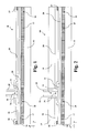
- Fig. 3 shows a cross-sectional view of an exemplary thin film photovoltaic device 10.
- the photovoltaic device 10 generally includes a glass substrate 12 oppositely positioned from an encapsulating substrate 14.
- the glass 12 can be referred to as a "superstrate,” as it is the substrate on which the subsequent layers are formed even though it faces upward to the radiation source (e.g., the sun) when the cadmium telluride thin film photovoltaic device 10 is in use.
- the top sheet of glass 12 can be a high-transmission glass (e.g., high transmission borosilicate glass), low-iron float glass, or other highly transparent glass material.
- the glass is generally thick enough to provide support for the subsequent film layers (e.g., from about 0.5 mm to about 10 mm thick), and is substantially flat to provide a good surface for forming the subsequent film layers.
- the glass 12 can be a low iron float glass containing less than about 0.015% by weight iron (Fe), and may have a transmissiveness of about 0.9 or greater in the spectrum of interest (e.g., wavelengths from about 300 nm to about 900 nm).
- borosilicate glass may be utilized so as to better withstand high temperature processing.
- the encapsulating substrate 14 defines a connection aperture 15 providing access to the underlying components to collect the DC electricity generated by the photovoltaic device 10.
- the encapsulating substrate 14 is a glass substrate.
- a plurality of thin film layers 16 are positioned on the glass substrate 12.
- the plurality of thin film layers 16 define individual photovoltaic cells 17 separated by scribes 18.
- the individual photovoltaic cells 17 are electrically connected together in series.
- the plurality of thin film layers can include a transparent conductive oxide layer (e.g., cadmium stannate or stoichiometric variation of cadmium, tin, and oxygen) on the glass substrate 12, a resistive transparent buffer layer (e.g., a combination of zinc oxide and tin oxide) on the transparent conductive oxide layer, an n-type layer on the resistive transparent buffer layer, a p-type layer on the n-type layer, and a back contact on the p-type layer.
- a transparent conductive oxide layer e.g., cadmium stannate or stoichiometric variation of cadmium, tin, and oxygen
- a resistive transparent buffer layer e.g., a combination
- the n-type layer can include cadmium sulfide (i.e., a cadmium sulfide thin film layer), and the p-type layer can include cadmium telluride (i.e., a cadmium telluride thin film layer).
- the back contact defines the exposed surface of the thin film layers 16, and serves as an electrical contact of the thin film layers opposite the front contact defined by the transparent conductive oxide layer.
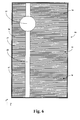
- Fig. 4 generally shows a top view of an exemplary thin film photovoltaic device 10 defining a plurality of photovoltaic cells 17 separated by scribes 18.
- the scribes 18 can be, in one embodiment, substantially parallel to each other such that the photovoltaic cells 17 are substantially the same size.
- each of the scribes 18 is generally oriented in the x-direction.
- the insulating layer 20 is on the thin film layers 16 to protect the back contact of the thin film layers 16.
- the insulating layer 20 generally includes an insulating material that can prevent electrical conductivity therethrough. Any suitable material can be used to produce the insulating layer 20.
- the insulating layer 20 can be an insulating polymeric film coated on both surfaces with an adhesive coating.
- the adhesive coating can allow for adhesion of the insulating layer 20 to the underlying thin film layers 16 and for the adhesion of the conductive strip 24 to the insulating layer 20.
- the insulating layer 20 can include a polymeric film of polyethylene terephthalate (PET) having an adhesive coating on either surface.
- PET polyethylene terephthalate
- the adhesive coating can be, for example, an acrylic adhesive, such as a thermosetting acrylic adhesive.
- the insulating layer 20 is a strip of insulating material generally oriented in a direction perpendicular to the orientation of the scribes 18.
- the insulating layer 20 can be generally oriented in the y-direction that is perpendicular to the orientation of the scribes 18 in the x-direction.
- the insulating layer 20 can have a thickness in the z-direction suitable to prevent electrical conductivity from the underlying thin film layers, particularly the back contact, to any subsequently applied layers. In one particular embodiment, the insulating layer 20 can prevent electrically conductivity between the thin film layers 16 and the conductive strip 24.
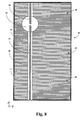
- the intra-laminate disk layer 22 is positioned on the thin film layers 16 over an area to be exposed by the connection aperture 15 of the encapsulating substrate 14.
- the intra-laminate disk layer 22 can extend over a protected area (as defined in the x- and y- directions on the surface of the thin film layers 16) that is larger than the connection aperture 15 defined by the encapsulating substrate 14 and/or that is that is larger than the adhesive gap 31 defined by the adhesive layer 30.
- the intra-laminate disk layer 22 defines a substantially circular disk in the x, y plane. This shape can be particularly useful when both the adhesive gap 31 defined in the adhesive layer 30 and the connection aperture 15 in the encapsulating substrate 14 are also substantially circular in the x, y plane. As such, the intra-laminate disk layer 22 can be substantially centered with respect to the adhesive gap 31 defined by the adhesive layer 30 and to the connection aperture 15 defined by the encapsulating substrate 14. Also, with this configuration, the disk diameter of the intra-laminate disk layer 22 can be larger than the gap diameter defined by the adhesive gap 31 and/or the aperture diameter defined by the connection aperture 15. For instance, the disk diameter can be at about 5% larger to about 200% larger than the gap diameter and/or the connection diameter, such as about 10% larger to about 100% larger.
- the intra-laminate disk layer can define a thickness, in the z-direction, of about 50 ⁇ m to about 400 ⁇ m.
- the intra-laminate disk layer 22 in one embodiment, can be constructed of a film having a polymeric coating on one or both surfaces.
- the polymeric coating can include a hydrophobic polymer configured to moisture ingress through the intra-laminate disk layer 22 and/or around the intra-laminate disk layer 22.
- the polymeric coating can help adhere the intra-laminate disk layer 22 to the underlying layers (e.g., the thin film layers 16) and subsequently applied layers (e.g., the adhesive layer 30).
- the polymeric coating can include an ethylene-vinyl acetate copolymer.
- the film can of the intra-laminate disk layer 22 can be a polymeric film.
- the polymeric film can include the same polymer as the polymeric coating or a different polymer.
- the film can be a polymeric film, including polymers such as polyethylene, polypropylene, polyethylene terephthalate (PET), ethylene-vinyl acetate copolymer, or copolymers or mixtures thereof.
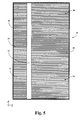
- the intra-laminate disk layer 22 can be applied after the insulating layer 20, such as shown in Figs. 5-6 to result in the embodiment of Fig. 3 .
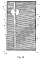
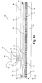
- the intra-laminate disk layer 22 can be applied before the insulating layer 20 (e.g., directly onto the plurality of thin film layers 16), such as shown in Figs. 11-14 .
- Figs. 11-14 show another exemplary thin film photovoltaic device 100 where the intra-laminate disk layer 22 is beneath the insulating layer 20 and directly over the plurality of thin film layers 16.
- the conductive strip 24, in one embodiment, can be applied as a continuous strip over the insulating layer 20, as shown in Fig. 7 . Then, the continuous strip can then be severed to produce a first lead 25 and a second lead 26.
- the conductive strip 24 can be constructed from any suitable material.
- the conductive strip 24 is a strip of metal foil.
- the metal foil can include a conductive metal.
- Bus bars 27, 28 can then be attached over opposite ends of the photovoltaic device 10.
- the first bus bar 27 can overly the photovoltaic cell 17 positioned at the first end of the photovoltaic device 10, while the second bus bar 28 overlies the photovoltaic cell 17 at the second end of the photovoltaic device 10 opposite the first end. Since the photovoltaic cells 17 are connected to each other in series, the bus bars 27, 28 can serve as opposite electrical connections (e.g., positive and negative) on the photovoltaic device 10.
- the conductive strip 24 electrically connects the opposite electrical bus bars 27, 28 to the first lead 25 and the second lead 26.
- the encapsulating substrate 14 can be adhered to the photovoltaic device 10 via an adhesive layer 30.
- the adhesive layer 30 is generally positioned over the conductive strip 24, intra-laminate disk layer 22, insulating layer 20, and any remaining exposed areas of the thin film layers 16.
- the adhesive layer 30 generally defines an adhesive gap 31 that generally corresponds to the connection aperture 15 defined by the encapsulating substrate 14. As such, the first lead 25 and second lead 26 can extend through the adhesive gap 31.
- the adhesive layer 30 can generally protect the thin film layers 16 and attach the encapsulating substrate 14 to the device 10.
- the adhesive layer 30 can be constructed from ethylene vinyl acetate (EVA), polyvinyl butyral (PVB), silicone based adhesives, or other adhesives which are configured to prevent moisture from penetrating the device.
- EVA ethylene vinyl acetate
- PVB polyvinyl butyral
- silicone based adhesives or other adhesives which are configured to prevent moisture from penetrating the device.
- Fig. 3 shows a junction box 32 configured to electrically connect the photovoltaic device 10 by completing the DC circuit.
- the junction box 32 can then provide a positive lead wire 33 and a negative lead wire 34 for further collection of the DC electricity produced by the photovoltaic device 10.
- Fig. 10 generally shows a flow diagram of one exemplary method 40 for construction of the exemplary photovoltaic device 10 of Fig. 3 .
- an insulating layer is applied on plurality of thin film layers at 41, and an intra-laminate disk layer is applied on the plurality of thin film layers at 42.
- a conductive strip can then be applied on the insulating layer at 43, and severed into a first conductive strip and a second conductive strip at 44.
- a first bus bar can be attached to the first conductive strip at 45, and a second bus bar can be attached to the second conductive strip at 46.
- steps 41-46 of method 40 are exemplified sequentially in Figs. 4-9 .
- Method 40 also includes attaching an adhesive layer, defming an adhesive gap, over the first conductive strip, the second conductive strip, the intra-laminate disk layer, the insulated layer, and any remaining exposed areas of the plurality of thin films at 47.
- An encapsulating substrate, defining a connection aperture, can be attached on the adhesive layer at 48.
- a junction box can be attached over the connection aperture and the adhesive gap at 49, and attached to the first conductive strip and the second conductive strip.
- steps 47-50 of method 40 are exemplified sequentially in Figs. 1-3 .
Landscapes
- Photovoltaic Devices (AREA)
Applications Claiming Priority (1)
| Application Number | Priority Date | Filing Date | Title |
|---|---|---|---|
| US12/870,013 US8513516B2 (en) | 2010-08-27 | 2010-08-27 | Intra-laminate disk layer for thin film photovoltaic devices and their methods of manufacture |
Publications (1)
| Publication Number | Publication Date |
|---|---|
| EP2423979A2 true EP2423979A2 (de) | 2012-02-29 |
Family
ID=44735817
Family Applications (1)
| Application Number | Title | Priority Date | Filing Date |
|---|---|---|---|
| EP11176913A Withdrawn EP2423979A2 (de) | 2010-08-27 | 2011-08-09 | Intralaminatscheibenschicht für Dünnfilmfotovoltaikvorrichtungen und Herstellungsverfahren dafür |
Country Status (3)
| Country | Link |
|---|---|
| US (1) | US8513516B2 (de) |
| EP (1) | EP2423979A2 (de) |
| CN (1) | CN102437215A (de) |
Families Citing this family (7)
| Publication number | Priority date | Publication date | Assignee | Title |
|---|---|---|---|---|
| KR20130051216A (ko) * | 2011-11-09 | 2013-05-20 | 엘지이노텍 주식회사 | 태양광 발전장치 |
| US20140060622A1 (en) * | 2012-08-31 | 2014-03-06 | Primestar Solar, Inc. | Direct connection of lead bar to conductive ribbon in a thin film photovoltaic device |
| US9331631B2 (en) * | 2012-08-31 | 2016-05-03 | First Solar, Inc. | Direct connection of lead bar to conductive ribbon in a thin film photovoltaic device |
| JP2015177169A (ja) * | 2014-03-18 | 2015-10-05 | シャープ株式会社 | 太陽電池モジュール |
| US10562274B1 (en) | 2016-02-22 | 2020-02-18 | Apple Inc. | Glass fastening and sealing systems |
| EP3573110A1 (de) * | 2018-05-25 | 2019-11-27 | (CNBM) Bengbu Design & Research Institute for Glass Industry Co., Ltd. | Solarmodul mit vergrösserter aperturfläche |
| CN120018687B (zh) * | 2025-04-21 | 2025-08-12 | 宁德时代新能源科技股份有限公司 | 电池组件及其制造方法、用电装置、发电装置 |
Family Cites Families (6)
| Publication number | Priority date | Publication date | Assignee | Title |
|---|---|---|---|---|
| US4371739A (en) * | 1981-10-16 | 1983-02-01 | Atlantic Richfield Company | Terminal assembly for solar panels |
| US5022930A (en) | 1989-06-20 | 1991-06-11 | Photon Energy, Inc. | Thin film photovoltaic panel and method |
| US6169246B1 (en) * | 1998-09-08 | 2001-01-02 | Midwest Research Institute | Photovoltaic devices comprising zinc stannate buffer layer and method for making |
| EP1801889B1 (de) * | 1999-09-01 | 2017-05-17 | Kaneka Corporation | Dünnschichtsolarzellenmodul und sein Herstellungsverfahren |
| US20090194165A1 (en) | 2008-01-31 | 2009-08-06 | Primestar Solar, Inc. | Ultra-high current density cadmium telluride photovoltaic modules |
| JP4384241B1 (ja) * | 2008-06-04 | 2009-12-16 | シャープ株式会社 | 端子ボックス及び太陽電池モジュール |
-
2010
- 2010-08-27 US US12/870,013 patent/US8513516B2/en not_active Expired - Fee Related
-
2011
- 2011-08-09 EP EP11176913A patent/EP2423979A2/de not_active Withdrawn
- 2011-08-25 CN CN2011102577912A patent/CN102437215A/zh active Pending
Non-Patent Citations (1)
| Title |
|---|
| None |
Also Published As
| Publication number | Publication date |
|---|---|
| US8513516B2 (en) | 2013-08-20 |
| CN102437215A (zh) | 2012-05-02 |
| US20120024349A1 (en) | 2012-02-02 |
Similar Documents
| Publication | Publication Date | Title |
|---|---|---|
| US6323416B1 (en) | Solar cell module | |
| US20120125391A1 (en) | Methods for interconnecting photovoltaic cells | |
| KR101091372B1 (ko) | 태양광 발전장치 | |
| US8513516B2 (en) | Intra-laminate disk layer for thin film photovoltaic devices and their methods of manufacture | |
| EP3179179A1 (de) | Photovoltaikanlage mit integrierter befestigungsstruktur und verfahren zur herstellung davon | |
| US9331213B2 (en) | Integrated power connectors for PV modules and their methods of manufacture | |
| US20190326459A1 (en) | Single-cell encapsulation and flexible-format module architecture and mounting assembly for photovoltaic power generation and method for constructing, inspecting and qualifying the same | |
| KR101652607B1 (ko) | 직렬 연결형 박막 태양광 모듈 및 박막 태양 전지의 직렬 연결 방법 | |
| EP2761674B1 (de) | Verbindungsstruktur von solarzellen | |
| US20130153004A1 (en) | Junction box with a support member for thin film photovoltaic devices and their methods of manufacture | |
| US20140102537A1 (en) | Photovoltaic module | |
| CN103515454A (zh) | 薄膜太阳能电池模块及其制造方法 | |
| WO2010141463A1 (en) | Dopant-containing contact material | |
| JP2012243996A (ja) | 薄膜シリコン系太陽電池モジュール | |
| US20110083734A1 (en) | Module moisture barrier | |
| WO2011053087A2 (ko) | 태양전지 및 이의 제조방법 | |
| CN102017179A (zh) | 集成有微型联接装置的绝缘玻璃部件 | |
| US20130153001A1 (en) | Support insert for thin film photovoltaic devices and their methods of manufacture | |
| US20130153003A1 (en) | Adhesive plug for thin film photovoltaic devices and their methods of manufacture | |
| US20130048055A1 (en) | Sealing layer for thin film photovoltaic devices and their methods of manufacture | |
| US20130153005A1 (en) | Reinforcement element for thin film photovoltaic devices and their methods of manufacture | |
| JPH11214734A (ja) | 太陽電池モジュールおよびその製造方法およびその施工方法および太陽電池発電システム | |
| WO2024216745A1 (zh) | 光伏背板、光伏背板的制作方法及光伏组件 | |
| US20120024339A1 (en) | Photovoltaic Module Including Transparent Sheet With Channel | |
| US20140246074A1 (en) | Solar module with ribbon cable, and a method for the manufacture of same |
Legal Events
| Date | Code | Title | Description |
|---|---|---|---|
| AK | Designated contracting states |
Kind code of ref document: A2 Designated state(s): AL AT BE BG CH CY CZ DE DK EE ES FI FR GB GR HR HU IE IS IT LI LT LU LV MC MK MT NL NO PL PT RO RS SE SI SK SM TR |
|
| AX | Request for extension of the european patent |
Extension state: BA ME |
|
| PUAI | Public reference made under article 153(3) epc to a published international application that has entered the european phase |
Free format text: ORIGINAL CODE: 0009012 |
|
| RAP1 | Party data changed (applicant data changed or rights of an application transferred) |
Owner name: FIRST SOLAR MALAYSIA SDN.BHD |
|
| STAA | Information on the status of an ep patent application or granted ep patent |
Free format text: STATUS: THE APPLICATION IS DEEMED TO BE WITHDRAWN |
|
| 18D | Application deemed to be withdrawn |
Effective date: 20150303 |