EP2422988A1 - Thermal head, thermal printer, and manufacturing method for the thermal head - Google Patents
Thermal head, thermal printer, and manufacturing method for the thermal head Download PDFInfo
- Publication number
- EP2422988A1 EP2422988A1 EP11175418A EP11175418A EP2422988A1 EP 2422988 A1 EP2422988 A1 EP 2422988A1 EP 11175418 A EP11175418 A EP 11175418A EP 11175418 A EP11175418 A EP 11175418A EP 2422988 A1 EP2422988 A1 EP 2422988A1
- Authority
- EP
- European Patent Office
- Prior art keywords
- heating resistor
- electrodes
- flat plate
- upper substrate
- substrate
- Prior art date
- Legal status (The legal status is an assumption and is not a legal conclusion. Google has not performed a legal analysis and makes no representation as to the accuracy of the status listed.)
- Granted
Links
Images




Classifications
-
- B—PERFORMING OPERATIONS; TRANSPORTING
- B41—PRINTING; LINING MACHINES; TYPEWRITERS; STAMPS
- B41J—TYPEWRITERS; SELECTIVE PRINTING MECHANISMS, i.e. MECHANISMS PRINTING OTHERWISE THAN FROM A FORME; CORRECTION OF TYPOGRAPHICAL ERRORS
- B41J2/00—Typewriters or selective printing mechanisms characterised by the printing or marking process for which they are designed
- B41J2/315—Typewriters or selective printing mechanisms characterised by the printing or marking process for which they are designed characterised by selective application of heat to a heat sensitive printing or impression-transfer material
- B41J2/32—Typewriters or selective printing mechanisms characterised by the printing or marking process for which they are designed characterised by selective application of heat to a heat sensitive printing or impression-transfer material using thermal heads
- B41J2/335—Structure of thermal heads
- B41J2/33585—Hollow parts under the heater
-
- B—PERFORMING OPERATIONS; TRANSPORTING
- B41—PRINTING; LINING MACHINES; TYPEWRITERS; STAMPS
- B41J—TYPEWRITERS; SELECTIVE PRINTING MECHANISMS, i.e. MECHANISMS PRINTING OTHERWISE THAN FROM A FORME; CORRECTION OF TYPOGRAPHICAL ERRORS
- B41J2/00—Typewriters or selective printing mechanisms characterised by the printing or marking process for which they are designed
- B41J2/315—Typewriters or selective printing mechanisms characterised by the printing or marking process for which they are designed characterised by selective application of heat to a heat sensitive printing or impression-transfer material
- B41J2/32—Typewriters or selective printing mechanisms characterised by the printing or marking process for which they are designed characterised by selective application of heat to a heat sensitive printing or impression-transfer material using thermal heads
- B41J2/335—Structure of thermal heads
- B41J2/33505—Constructional details
- B41J2/3351—Electrode layers
-
- B—PERFORMING OPERATIONS; TRANSPORTING
- B41—PRINTING; LINING MACHINES; TYPEWRITERS; STAMPS
- B41J—TYPEWRITERS; SELECTIVE PRINTING MECHANISMS, i.e. MECHANISMS PRINTING OTHERWISE THAN FROM A FORME; CORRECTION OF TYPOGRAPHICAL ERRORS
- B41J2/00—Typewriters or selective printing mechanisms characterised by the printing or marking process for which they are designed
- B41J2/315—Typewriters or selective printing mechanisms characterised by the printing or marking process for which they are designed characterised by selective application of heat to a heat sensitive printing or impression-transfer material
- B41J2/32—Typewriters or selective printing mechanisms characterised by the printing or marking process for which they are designed characterised by selective application of heat to a heat sensitive printing or impression-transfer material using thermal heads
- B41J2/335—Structure of thermal heads
- B41J2/3354—Structure of thermal heads characterised by geometry
-
- Y—GENERAL TAGGING OF NEW TECHNOLOGICAL DEVELOPMENTS; GENERAL TAGGING OF CROSS-SECTIONAL TECHNOLOGIES SPANNING OVER SEVERAL SECTIONS OF THE IPC; TECHNICAL SUBJECTS COVERED BY FORMER USPC CROSS-REFERENCE ART COLLECTIONS [XRACs] AND DIGESTS
- Y10—TECHNICAL SUBJECTS COVERED BY FORMER USPC
- Y10T—TECHNICAL SUBJECTS COVERED BY FORMER US CLASSIFICATION
- Y10T29/00—Metal working
- Y10T29/49—Method of mechanical manufacture
- Y10T29/49002—Electrical device making
Definitions
- the present invention relates to a thermal head, a thermal printer, and a manufacturing method for the thermal head.
- thermal head for use in thermal printers (see, for example, Japanese Patent Application Laid-open No. 2009-119850 ).
- a plurality of heating resistors are formed on a stacked substrate of a support substrate and an upper substrate, and power is supplied to pairs of electrodes connected to the heating resistors, thereby allowing the heating resistors to generate heat to perform printing on a thermal recording medium or the like.
- a cavity portion is formed at a position opposed to each of the heating resistors in a bonding portion between the support substrate and the upper substrate.
- the cavity portion functions as a heat insulating layer of low thermal conductivity to reduce an amount of heat to be transferred from the heating resistor toward the support substrate via the upper substrate, to thereby increase thermal efficiency and reduce power consumption.
- the electrodes are designed in consideration of the electrical resistance from external input terminals to the heating resistor. As the ratio of the electrical resistance of the electrode to the electrical resistance of the heating resistor becomes larger, a larger power loss occurs by voltage drop of the electrical resistance from the external input terminals to the heating resistor. It is therefore necessary to decrease the electrical resistance of the electrode.
- the electrical resistance of the electrode can be decreased by thickening the electrode.
- the conventional thermal head has a problem that heat insulating performance exerted by the cavity portion cannot be fully utilized because the heat dissipates from the heating resistor in the planar direction of the upper substrate via the electrodes.
- the present invention has been made in view of the above-mentioned circumstances, and it is therefore an object of the present invention to provide a thermal head which is capable of suppressing diffusion of heat from a heating resistor in a planar direction of an upper substrate via electrodes so that printing efficiency may be increased, and also provide a printer including the thermal head. Further, it is another object of the present invention to provide a method of manufacturing the thermal head with ease.
- the present invention provides the following measures.
- the present invention provides a thermal head including: a stacked substrate including a flat plate-shaped support substrate and a flat plate-shaped upper substrate which are bonded to each other in a stacked state; a heating resistor formed on a surface of the flat plate-shaped upper substrate; and a pair of electrodes connected to both ends of the heating resistor, respectively, for supplying power to the heating resistor, in which the stacked substrate includes a cavity portion in a region opposed to the heating resistor at a bonding portion between the flat plate-shaped support substrate and the flat plate-shaped upper substrate, and at least one of the pair of electrodes includes a thin portion in a region opposed to the cavity portion, the thin portion being thinner than other regions of the pair of electrodes.
- the upper substrate disposed directly under the heating resistor functions as a heat storage layer that stores heat
- the cavity portion formed in the region opposed to the heating resistor functions as a hollow heat insulating layer that blocks the heat. Because of the formation of the cavity portion, among an amount of heat generated by the heating resistor, an amount of heat transferring toward the support substrate via the upper substrate can be reduced.
- the heat generated by the heating resistor diffuses also in the planar direction of the upper substrate via the electrodes.
- the thin portion of at least one of the electrodes, which is disposed above the cavity portion has thermal conductivity lower than other regions of the electrodes. Therefore, the heat generated from the heating resistor can be prevented from easily transferring to the outside of the region opposed to the cavity portion. This suppresses the diffusion of the heat, which is prevented by the cavity portion from transferring toward the support substrate, in the planar direction of the upper substrate via the electrodes. Therefore, the heat can be transferred to an opposite side of the support substrate to increase printing efficiency.
- the thin portion may extend to an outside of the region opposed to the cavity portion.
- the region of low thermal conductivity of the electrode extends to the outside of the region opposed to the cavity portion. Accordingly, the diffusion of heat from the heating resistor in the planar direction of the upper substrate via the electrodes can be suppressed more. Therefore, high heat insulating performance exerted by the cavity portion can be fully utilized.
- both of the pair of electrodes may include the thin portions.
- the heat generated from the heating resistor can be prevented from easily transferring to the outside of the region opposed to the cavity portion. Therefore, the diffusion of heat in the planar direction of the upper substrate via the electrodes can be suppressed more effectively.
- the present invention provides a thermal head including: a stacked substrate including a flat plate-shaped support substrate and a flat plate-shaped upper substrate which are bonded to each other in a stacked state; a rectangular-shaped heating resistor formed on a surface of the flat plate-shaped upper substrate; and a pair of electrodes connected to both ends of the rectangular-shaped heating resistor, respectively, for supplying power to the rectangular-shaped heating resistor, in which the stacked substrate includes a cavity portion in a region opposed to the rectangular-shaped heating resistor at a bonding portion between the flat plate-shaped support substrate and the flat plate-shaped upper substrate, and at least one of the pair of electrodes includes a low thermal conductivity portion in a region opposed to the cavity portion, the low thermal conductivity portion being made of a material having thermal conductivity lower than other regions of the pair of electrodes and having an electrical resistance lower than an electrical resistance of the rectangular-shaped heating resistor.
- the low thermal conductivity portion of at least one of the electrodes, which is disposed above the cavity portion has an electrical resistance lower than that of the heating resistor. Accordingly, sufficient power can be supplied to the heating resistor. Further, the thermal conductivity of the low thermal conductivity portion is lower than the other regions of the electrodes, and hence the heat generated from the heating resistor can be prevented from easily transferring to the outside of the region opposed to the cavity portion. This suppresses the diffusion of the heat, which is prevented by the cavity portion from transferring toward the support substrate, in the planar direction of the upper substrate via the electrodes. Therefore, the heat can be transferred to an opposite side of the support substrate to increase printing efficiency.
- the low thermal conductivity portion may extend to an outside of the region opposed to the cavity portion.
- the region of low thermal conductivity of the electrode extends to the outside of the region opposed to the cavity portion. Accordingly, the diffusion of heat from the heating resistor in the planar direction of the upper substrate via the electrodes can be suppressed more.
- both of the pair of electrodes may include the low thermal conductivity portions.
- the heat generated from the heating resistor can be prevented from easily transferring to the outside of the region opposed to the cavity portion. Therefore, the diffusion of heat in the planar direction of the upper substrate via the electrodes can be suppressed more effectively.
- the present invention provides a printer including: the thermal head according to the above-mentioned invention; and a pressure mechanism for feeding a thermal recording medium while pressing the thermal recording medium against the heating resistor of the thermal head.
- the thermal head having excellent thermal efficiency is used, and hence the heat generated by the heating resistor can be transferred with high efficiency to the thermal recording medium that is pressed against the heating resistor by the pressure mechanism. Therefore, power consumption during printing on the thermal recording medium can be reduced to extend the battery duration.
- the present invention provides a manufacturing method for a thermal head, including: a bonding step of bonding a flat plate-shaped upper substrate in a stacked state to a flat plate-shaped support substrate including a concave portion opened in a surface of the flat plate-shaped support substrate, so as to close the concave portion to form a cavity portion; a heating resistor forming step of forming a heating resistor on a surface of the flat plate-shaped upper substrate, which is bonded to the flat plate-shaped support substrate in the bonding step, at a position opposed to the concave portion; and an electrode forming step of forming a pair of electrodes to be connected to both ends of the heating resistor, respectively, on the flat plate-shaped upper substrate on which the heating resistor is formed in the heating resistor forming step, in which the electrode forming step includes: a first forming step of forming a first layer constituting the pair of electrodes; and a second forming step of forming, at a substantially uniform thickness, a second layer constituting at least one
- the concave portion of the support substrate is closed by the upper substrate, to thereby form the cavity portion at a bonding portion between the support substrate and the upper substrate.
- the cavity portion functions as a hollow heat insulating layer that blocks heat generated by the heating resistor. Therefore, an amount of heat to be transferred from the heating resistor toward the support substrate can be reduced.
- the second layer having a substantially uniform thickness is simply formed on the surface of the first layer, which is formed in the first forming step, and on the surface of the heating resistor in the region opposed to the cavity portion.
- the electrode in which, in the region opposed to the cavity portion, a thin portion having a thickness smaller than other regions by the thickness of the first layer is disposed.
- the thin portion of the electrode has thermal conductivity lower than other regions of the electrodes, and hence the heat generated from the heating resistor can be prevented from easily transferring to the outside of the region opposed to the cavity portion. This suppresses diffusion of the heat, which is prevented by the cavity portion from transferring toward the support substrate, in the planar direction of the upper substrate via the electrodes. Therefore, a thermal head with increased printing efficiency can be manufactured with ease.
- the present invention provides a manufacturing method for a thermal head, including: a bonding step of bonding a flat plate-shaped upper substrate in a stacked state to a flat plate-shaped support substrate including a concave portion opened in a surface of the flat plate-shaped support substrate, so as to close the concave portion to form a cavity portion; a heating resistor forming step of forming a heating resistor on a surface of the flat plate-shaped upper substrate, which is bonded to the flat plate-shaped support substrate in the bonding step, at a position opposed to the concave portion; and an electrode forming step of forming a pair of electrodes to be connected to both ends of the heating resistor, respectively, on the flat plate-shaped upper substrate on which the heating resistor is formed in the heating resistor forming step, in which the electrode forming step includes: a first forming step of forming the pair of thick electrodes; and a second forming step of forming a thin portion in a region of at least one of the pair of thick electrodes opposed to the
- the thick electrode formed in the first forming step is simply thinned in part in the second forming step.
- the electrode in which thermal conductivity in the region opposed to the cavity portion is lower than thermal conductivity in other regions.
- the formation of the thin portion of the electrode suppresses diffusion of heat from the heating resistor in the planar direction of the upper substrate. Therefore, a thermal head with increased printing efficiency can be manufactured with ease.
- the present invention provides the effect that diffusion of heat from the heating resistor in the planar direction of the upper substrate via the electrodes can be suppressed so that printing efficiency may be increased. Further, the present invention provides the effect that the thermal head with increased printing efficiency can be manufactured with ease.
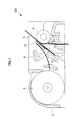
- a thermal printer (printer) 100 includes a main body frame 2, a platen roller 4 disposed horizontally, a thermal head 10 disposed so as to be opposed to an outer peripheral surface of the platen roller 4, a paper feeding mechanism 6 for feeding an object to be printed, such as thermal paper (thermal recording medium) 3, between the platen roller 4 and the thermal head 10, and a pressure mechanism 8 for pressing the thermal head 10 against the thermal paper 3 with a predetermined pressing force.
- the thermal paper 3 and the thermal head 10 are pressed by the operation of the pressure mechanism 8. Accordingly, a load of the platen roller 4 is applied to the thermal head 10 via the thermal paper 3.
- the thermal head 10 includes a substrate main body (stacked substrate) 13, a plurality of heating resistors 15 formed on the substrate main body 13, pairs of electrodes 17A and 17B connected to both ends of the heating resistors 15, and a protective film 19 for covering and protecting, against abrasion and corrosion, the heating resistors 15 and the electrodes 17A and 17B on the substrate main body 13.
- the arrow Y represents a feeding direction of the thermal paper 3 by the platen roller 4.
- the substrate main body 13 is fixed to a heat dissipation plate (not shown) as a plate-shaped member made of a metal such as aluminum, a resin, ceramics, glass, or the like, to thereby dissipate heat via the heat dissipation plate.
- the substrate main body 13 includes a flat plate-shaped support substrate 12 that is fixed to the heat dissipation plate, and a flat plate-shaped upper substrate 14 that is bonded to a surface of the support substrate 12 in a stacked state.
- the support substrate 12 is, for example, a rectangular-shaped glass substrate or ceramic substrate having a thickness approximately ranging from 300 ⁇ m to 1 mm.
- a concave portion 21 that is opened in a rectangular shape at a bonding surface to the upper substrate 14.
- the concave portion 21 extends along the longitudinal direction of the support substrate 12, and has a width dimension of, for example, 50 ⁇ m to 500 ⁇ m.
- the upper substrate 14 is, for example, a rectangular-shaped glass substrate having a thickness approximately ranging from 5 ⁇ m to 100 ⁇ m.
- the upper substrate 14 is stacked onto the surface of the support substrate 12 so as to close the concave portion 21.
- the plurality of heating resistors 15 are provided on the surface of the upper substrate 14 so that the upper substrate 14 functions as a heat storage layer that stores a part of the heat generated by the heating resistors 15.
- the heating resistor 15 is made of, for example, a Ta-based or silicide-based material and formed into a rectangular shape. Further, the heating resistor 15 has a dimension that the length in the longitudinal direction thereof is larger than the width dimension of the concave portion 21 of the support substrate 12.
- the heating resistors 15 are arrayed at predetermined intervals along the longitudinal direction of the upper substrate 14 (longitudinal direction of the concave portion 21 of the support substrate 12), with the longitudinal direction of the heating resistors 15 aligned with the width direction of the upper substrate 14. In other words, the heating resistors 15 are each provided so as to straddle the concave portion 21 of the support substrate 12 in its width direction.
- the electrodes 17A and 17B include an integrated electrode 17A connected to one end of all the heating resistors 15 in the longitudinal direction thereof, and a plurality of electrodes 17B individually connected to another end of each of the heating resistors 15. Further, the electrodes 17A and 17B are connected to the heating resistor 15 so as to overlap the surface of the heating resistor 15.
- the material used for the electrodes 17A and 17B is, for example, aluminum.
- the heating resistor 15 has a heating region corresponding to a portion positioned between the electrode 17A and the electrode 17B, that is, a portion positioned substantially directly above the concave portion 21 of the support substrate 12.
- the heating region of the heating resistor 15 is referred to as heating portion 15a.
- the surface of the protective film 19 covering the heating portions 15a of the heating resistors 15 serves as a printing portion with respect to the thermal paper 3, that is, a head portion 19a.
- the pair of electrodes 17A and 17B be arranged so that a length (heater length) Lr of the heating portion 15a extending in the longitudinal direction of the heating resistor 15 may be smaller than a distance (inter-dot distance or dot pitch) Wd between the center positions of adjacent heating resistors 15.
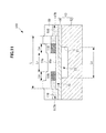
- each of the electrodes 17A and 17B has a thin portion 18 at a connecting portion disposed on the surface of the heating resistor 15.
- the thin portion 18 is thinner than other regions (hereinafter, a portion in the other regions is referred to as thick portion 16).
- each of the electrodes 17A and 17B is formed so that a portion disposed on the upper substrate 14 and a part of the connecting portion disposed on the heating resistor 15 may be thick while the rest of the connecting portion disposed on the heating resistor 15 may be thin.
- the thick portion 16 has a thickness te1 of, for example, 1 ⁇ m to 3 ⁇ m. It is desired to set the thickness te1 of the thick portion 16 to fall in such a range that can secure a sufficient electrical resistance so that the electrical resistance of the thick portion 16 may be, for example, approximately 1/10 of the electrical resistance of the heating resistor 15 or lower.
- the thin portion 18 is formed from the inside to the outside of the region of the heating resistor 15 opposed to the concave portion 21.
- a thickness te2 of the thin portion 18 is designed in consideration of, for example, the thickness te1 and the thermal conductivity of the thick portion 16 (the thermal conductivity of A1 is approximately 200 W/(m ⁇ °C)) and the thickness and the thermal conductivity of the upper substrate 14 (the thermal conductivity of commonly-used glass is approximately 1 W/(m ⁇ °C)).
- the thickness te2 of the thin portion 18 When the thickness te2 of the thin portion 18 is set smaller than the thickness te1 of the thick portion 16, the thermal conductivity of the electrodes 17A and 17B is reduced in part and heat insulating efficiency is increased.
- the thickness te2 of the thin portion 18 8 is set too small (for example, when the thickness te2 of the thin portion 18 is set to smaller than 10 nm), the electrical resistances of the electrodes 17A and 17B are increased in part, with the result that a power loss at the thin portion 18 exceeds the amount obtained by increasing the heat insulating efficiency.
- the thickness te2 of the thin portion 18 needs to be set considering a thickness that can be obtained by sputtering as a thin film. Therefore, it is desired to set the thickness te2 of the thin portion 18 to, for example, approximately 50 nm to approximately 300 nm.
- the thermal conductivity of the electrodes 17A and 17B is reduced in part and the heat insulating efficiency is increased.
- the electrical resistances of the electrodes 17A and 17B are increased in part, with the result that a power loss at the thin portion 18 exceeds the amount obtained by increasing the heat insulating efficiency. Therefore, it is desired to determine the length Le of the thin portion 18 so that the electrical resistance of each of the thin portions 18 may be 1/10 of the electrical resistance of the heating portion 15a or lower.
- the thin portion 18 be disposed within the width (nip width) in a range in which the platen roller 4 and the head portion 19a are brought into contact with each other through the thermal paper 3.
- the nip width is varied depending on the diameter and material of the platen roller 4, it is expected that the nip width generally correspond to a length L in the longitudinal direction of the heating resistor 15 as illustrated in FIG 3 .
- a width dimension (Lr+2Le) from the thin portion 18 of one electrode 17A to the thin portion 18 of the other electrode 17B is set within approximately 2 mm (within approximately 1 mm from the center position of the heating portion 15a).
- the thick portion 16 provided on the heating resistor 15 is also disposed within the nip width.
- Each of the electrodes 17A and 17B having the above-mentioned shapes has a two-stage structure in which a part of the thick portion 16 and the entire thin portion 18 are disposed on the heating resistor 15.
- the region disposed at a step portion between the heating resistor 15 and the upper substrate 14 is formed thick (as the thick portion 16). In this manner, disconnection of the electrodes 17A and 17B and an abnormal increase in electrical resistance caused by the step can be prevented to increase the heat insulating efficiency and increase the reliability of the thermal head 10.
- the opening of the concave portion 21 of the support substrate 12 is closed by the upper substrate 14, to thereby form a cavity portion 23 directly under the heating portion 15a of the heating resistor 15.
- the cavity portion 23 has a communication structure opposed to all the heating resistors 15. Further, the cavity portion 23 functions as a hollow heat insulating layer for preventing heat generated by the heating portions 15a from transferring toward the support substrate 12 from the upper substrate 14.
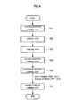
- the manufacturing method for the thermal head 10 includes a step of forming the substrate main body 13 and a step of forming the heating resistors 15, the electrodes 17A and 17B, and the protective film 19 on the substrate main body 13.
- the step of forming the substrate main body 13 includes a concave portion forming step SA1 of forming the concave portion 21 in the surface of the support substrate 12, a bonding step SA2 of bonding the support substrate 12 and the upper substrate 14 to each other, and a thinning step SA3 of thinning the upper substrate 14.
- the step of forming the heating resistors 15 and the like includes a heating resistor forming step SA4 of forming the heating resistors 15 on the substrate main body 13, an electrode forming step SA5 of forming the electrodes 17A and 17B, and a protective film forming step SA6 of forming the protective film 19.
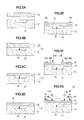
- the concave portion 21 is formed in the surface of the support substrate 12 in a position to be opposed to the heating resistors 15.
- the concave portion 21 is formed in the surface of the support substrate 12 by, for example, sandblasting, dry etching, wet etching, or laser machining.
- the thin glass (upper substrate) 14 having a thickness of, for example, 100 ⁇ m or more is bonded in a stacked state to the surface of the support substrate 12 in which the concave portion 21 is formed.
- the upper substrate 14 closes the opening of the concave portion 21 to form the cavity portion 23 between the support substrate 12 and the upper substrate 14.
- the thickness of the cavity portion 23 is defined by the depth of the concave portion 21, which makes it easy to control the thickness of the cavity portion 23 serving as the hollow heat insulating layer.
- An example of the bonding method for the support substrate 12 and the upper substrate 14 is direct bonding by thermal fusion.
- the support substrate 12 and the upper substrate 14 are bonded to each other at room temperature and then subjected to thermal fusion at high temperature.
- the resultant can be sufficiently high in bonding strength. It is desired that the bonding be performed at the softening temperature or lower in order to prevent deformation of the upper substrate 14.
- the upper substrate 14 is thinned by etching, polishing, or the like so as to have a desired small thickness.
- the upper substrate 14 it is difficult to manufacture and handle a substrate having a thickness of 100 ⁇ m or less, and such a substrate is expensive.
- the upper substrate 14 instead of directly bonding an originally thin upper substrate 14 onto the support substrate 12, the upper substrate 14 which is thick enough to be easily manufactured and handled is bonded onto the support substrate 12. After that, the upper substrate 14 is thinned. This enables a very thin upper substrate 14 to be formed on the surface of the support substrate 12 with ease at low cost. In this manner, the substrate main body 13 is formed.
- a thin film of the material of the heating resistors is formed on the upper substrate 14 of the substrate main body 13 by a thin film formation method such as sputtering, chemical vapor deposition (CVD), or deposition. Then, the thin film of the material of the heating resistors is molded by lift-off, etching, or the like.
- the electrode forming step SA5 includes a first forming step SA5-1 of forming, as illustrated in FIG 5E , a lower layer (hereinafter, referred to as first layer 16a) of the thick portion 16 of each of the electrodes 17A and 17B, and a second forming step SA5-2 of forming, as illustrated in FIG 5F , a second layer 18a on top of the first layer 16a, which is formed in the first forming step SA5-1.
- the first layers 16a are formed from both end portions of the heating resistor 15 in the longitudinal direction thereof to the upper substrate 14 and outside the region opposed to the cavity portion 23.
- the first layer 16a is formed in a manner that a film of a wiring material such as Al, Al-Si, Au, Ag, Cu, or Pt is deposited by sputtering, vapor deposition, or the like. Then, the film thus obtained is formed by lift-off or etching, or alternatively the wiring material is baked after screen-printing, to thereby form the first layer 16a having a desired shape.
- a wiring material such as Al, Al-Si, Au, Ag, Cu, or Pt
- the second layers 18a are formed at a substantially uniform thickness on the surface of the heating resistor 15 from inside the region opposed to the cavity portion 23 and over the first layers 16a.
- the second layer 18a is formed in a manner that a film of the same material as that of the first layer 16a is deposited by sputtering, vapor deposition, or the like. Then, the film thus obtained is formed by lift-off or etching, or alternatively the wiring material is baked after screen-printing, to thereby form the second layer 18a having a desired shape.
- the second layer 18a having a substantially uniform thickness is formed on each of the surface of the first layer 16a and the surface of the heating resistor 15. In this manner, it is possible to form the electrodes 17A and 17B, each of which has a stepped shape including the thick portion 16 and the thin portion 18 which is thinner than the thick portion 16 by the thickness of the first layer 16a.
- the protective film 19 is formed so as to cover the heating resistor 15 and the electrodes 17A and 17B formed on the upper substrate 14.
- the protective film 19 is formed in a manner that a film of a protective film material such as SiO 2 , Ta 2 O 5 , SiAlON, Si 3 N 4 , or diamond-like carbon is deposited on the upper substrate 14 by sputtering, ion plating, CVD, or the like.
- the thermal head 10 is completed, in which the substrate main body 13 has the cavity portion 23 at the bonding portion between the support substrate 12 and the upper substrate 14, and the electrodes 17A and 17B each have the thin portion 18 in the region of the heating resistor 15 opposed to the cavity portion 23.
- a voltage is selectively applied to the individual electrodes 17B of the thermal head 10. Then, a current flows through the heating resistors 15 which are connected to the selected electrodes 17B and the electrode 17A opposed thereto, to thereby allow the heating portions 15a to generate heat.
- the pressure mechanism 8 is operated to press the thermal head 10 against the thermal paper 3 being fed by the platen roller 4.
- the platen roller 4 rotates about an axis parallel to the array direction of the heating resistors 15, to thereby feed the thermal paper 3 toward the Y direction orthogonal to the array direction of the heating resistors 15.
- the head portion 19a is pressed, so that color is developed on the thermal paper 3, to thereby perform printing.
- the cavity portion 23 of the substrate main body 13 functions as the hollow heat insulating layer, and hence among an amount of heat generated by the heating resistor 15a, an amount of heat transferring toward the support substrate 12 via the upper substrate 14 can be reduced.
- the heat generated by the heating resistor 15 diffuses also in the planar direction of the upper substrate 14 via the electrodes 17A and 17B. Therefore, the length Le of the thin portion 18 of each of the electrodes 17A and 17B is a parameter affecting the heating efficiency.
- the thin portion 18 is disposed inside and outside the region of the surface of the heating resistor 15 opposed to the cavity portion 23, and hence each of the electrodes 17A and 17B has a region of low thermal conductivity which extends from the inside to the outside of the region opposed to the cavity portion 23. Accordingly, the heat generated from the heating resistor 15 can be prevented from easily transferring to the outside of the region opposed to the cavity portion 23, to thereby reduce the diffusion of heat in the planar direction of the upper substrate 14. Further, high heat insulating effect by the cavity portion 23 can be fully utilized.
- the heat generated from the heating resistor 15 is prevented from easily transferring to the outside of the region opposed to the cavity portion 23, and hence the diffusion of heat in the planar direction of the upper substrate 14 via the electrodes 17A and 17B can be suppressed more effectively.
- the formation of the thin portions 18 allows a small step to be formed between the heating resistor 15 and the electrodes 17A and 17B, and hence an air gap due to the step formed between the surface of the protective film 19 and the thermal paper 3 can be reduced as well. This can increase heat transfer efficiency toward the thermal paper 3.
- the heater length Lr of the heating portion of the heating resistor is designed to be the same as or larger than the length of the inter-dot distance (dot pitch) Wd.
- the heater length Lr of the heating portion is designed to be smaller than the inter-dot distance Wd.
- a thermal head employed in the multi-step printing method has a short heater length Lr of the heating portion, and hence the effective volume of the upper substrate positioned directly under the heating portion is reduced and an effective heat capacity C of the upper substrate is reduced.
- a temperature rise ⁇ T and the heat capacity C for one pulse has a relationship of ⁇ T ⁇ 1/C. Therefore, in the multi-step printing method, a large temperature rise ⁇ T can be obtained.
- the length of the heating portion is shortened, the ratio of the area covered by the electrodes with respect to the whole area of the cavity portion of the substrate main body is increased. In this case, dissipation of heat in the planar direction of the upper substrate via the electrodes becomes large to increase the thermal conductivity G Therefore, if the multi-step printing method is used without forming the thin portions in the electrodes, the heat insulating effect by the cavity portion cannot be utilized effectively. Further, performance (heat storage performance) of storing input energy in the heating portion is inversely proportional to the time constant ⁇ . Therefore, if the multi-step printing method is used without forming the thin portions in the electrodes, the heat storage effect is reduced. As a result, the thermal head which has a short heater length Lr of the heating portion to be employed in the multi-step printing method suffered a problem that high heating effect cannot be obtained.
- the thin portions 18 can suppress diffusion of heat in the planar direction of the upper substrate 14 via the electrodes 17A and 17B, respectively, to thereby suppress an increase in the thermal conductivity G Therefore, when the heater length Lr of the heating portion 15a is shortened to be smaller than the inter-dot distance (dot pitch) Wd (Lc ⁇ 2Le+Lr, Lr ⁇ Wd), it is possible to effectively take advantage of an effective reduction in heat capacity of the upper substrate 14, which is inherent in the thermal head 10 having a short heater length Lr of the heating portion 15a. In this manner, high heating efficiency and high-speed response can be achieved at the same time.
- the thickness of each of the electrodes 17A and 17B disposed above the cavity portion 23 is reduced in part so as to reduce the thermal conductivity thereof, and hence diffusion of heat in the planar direction of the upper substrate 14 via the electrodes 17A and 17B can be suppressed. This allows the heat generated from the heating portion 15a to effectively transfer to the head portion 19a so that printing efficiency may be increased.
- the thermal head 10 as described above is provided, and hence power consumption during printing on the thermal recording medium may be reduced to extend the battery duration. Further, according to the manufacturing method for a thermal head according to this embodiment, the thermal head 10 as described above can be manufactured with ease.
- each of the electrodes 17A and 17B is disposed from the inside to the outside of the region of the heating resistor 15 opposed to the cavity portion 23.
- each of the electrodes 17A and 17B may include a thin portion 18 only inside the region of the heating resistor 15 opposed to the cavity portion 23.
- the thin portion 18 may be formed in only one of the electrodes 17A and 17B, and the other electrode may be formed only of the thick portion 16.
- the electrodes 17A and 17B may each have a stepped shape with three steps or more in which the thickness of the electrode 17A or 17B is reduced in stages from the thick portion 16 side.
- the electrodes 17A and 17B may each have a thin portion 18 having a shape which is inclined so that the thickness of the connecting portion of the electrode 17A or 17B may be reduced gradually toward the distal end thereof.
- the thermal conductivity of the electrodes 17A and 17B above the cavity portion 23 is reduced so as to suppress diffusion of heat generated from the heating portion 15a in the planar direction of the upper substrate 14.
- the upper substrate 14 having a thickness of 100 ⁇ m or larger is used in the above.
- an originally thin glass (upper substrate 14) having a thickness ranging from 5 ⁇ m to 100 ⁇ m may be bonded in a stacked state to the surface of the support substrate 12 in which the cavity portion 23 is formed. This can omit the thinning step SA3 and shortens a manufacturing time.
- the first layer 16a is formed in the first forming step SA5-1 and the second layer 18a is formed in the second forming step SA5-2.
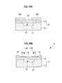
- a preliminary electrode 16b having a substantially uniform thickness approximately ranging from 1 ⁇ m to 3 ⁇ m as a whole, which is the same thickness of the thick portion 16, may be formed.
- the thin portion 18 may be formed in a region of the preliminary electrode 16b opposed to the cavity portion 23.
- the same method as the method of forming the above-mentioned first layer 16a may be employed to form the preliminary electrode 16b into an electrode pattern having a substantially uniform thickness.
- etching may be used to thin a part of the preliminary electrode 16b provided above the cavity portion 23.
- the thermal head 10 with increased printing efficiency can be manufactured with ease.
- thermal head a printer, and a manufacturing method for a thermal head according to a second embodiment of the present invention are described.
- a thermal head 110 according to this embodiment is different from the thermal head 10 according to the first embodiment in that electrodes 117A and 117B each include a low thermal conductivity portion 118, which is provided in a region opposed to the cavity portion 23 and made of a material having thermal conductivity lower than other regions and having an electrical resistance lower than that of the heating resistor 15.
- electrodes 117A and 117B each include a low thermal conductivity portion 118, which is provided in a region opposed to the cavity portion 23 and made of a material having thermal conductivity lower than other regions and having an electrical resistance lower than that of the heating resistor 15.
- the electrodes 117A and 117B have a substantially uniform thickness as a whole, although the low thermal conductivity portion 118 may be either thicker or thinner than other portions of the electrode 117.
- a portion disposed on the upper substrate 14 and a part of a connecting portion disposed on the heating resistor 15 are formed of a material of A1 (thermal conductivity: 223 W/(m ⁇ K), electrical resistance: 26.6 n ⁇ m) (hereinafter, this portion is referred to as "normal electrode 116"), and the remaining part of the connecting portion disposed on the heating resistor 15 is the low thermal conductivity portion 118.
- the low thermal conductivity portions 118 are formed of such a material as Pd (thermal conductivity: 71.4 W/(m ⁇ K), electrical resistance: 103 n ⁇ m), Pt (thermal conductivity: 71.4 W/(m ⁇ K), electrical resistance: 106 n ⁇ m), Mo (thermal conductivity: 147 W/(m ⁇ K), electrical resistance: 57.8 n ⁇ m), Nb (thermal conductivity: 52.5 W/(m ⁇ K), electrical resistance: 146 n ⁇ m), Ta (thermal conductivity: 54.6 W/(m ⁇ K), electrical resistance: 136 n ⁇ m), Ti (thermal conductivity 17.1 W/(m ⁇ K), electrical resistance: 420 ⁇ m), V (thermal conductivity: 31.1 W/(m ⁇ K), electrical resistance: 248 ⁇ m), or Zr (thermal conductivity: 22.7 W/(m ⁇ K), electrical resistance: 420 n ⁇ m).
- the low thermal conductivity portions 118 are each disposed on the heating resistor 15 5 from the inside to the outside of the region opposed to the cavity portion 23. Further, it is desired to determine a length Le of the heating resistor 15 in the low thermal conductivity portion 118 so that the electrical resistance of each of the low thermal conductivity portions 118 may be 1/10 of the electrical resistance of the heating portion 15a or lower. It is also desired to arrange the pair of electrodes 117A and 117B so that a heater length Lr of the heating resistor 15 may be shorter than the distance (inter-dot distance or dot pitch) Wd between the center positions of adjacent heating resistors 15. This arrangement provides the same effect as that of the thermal head 10 according to the first embodiment. In general, a material of low thermal conductivity has high electrical resistivity. Therefore, the length Le of the low thermal conductivity portion 118 is a parameter affecting the heating efficiency.
- the low thermal conductivity portion 118 of each of the electrodes 117A and 117B, which is disposed above the cavity portion 23, has an electrical resistance lower than that of the heating resistor 15. Therefore, sufficient power may be supplied to the heating resistor 15. Further, thermal conductivity of the low thermal conductivity portions 118 is lower than that of the normal electrodes 116, and hence heat generated from the heating resistor 15 can be prevented from easily transferring to the outside of the region opposed to the cavity portion 23.
Landscapes
- Physics & Mathematics (AREA)
- Geometry (AREA)
- Electronic Switches (AREA)
Abstract
Description
- The present invention relates to a thermal head, a thermal printer, and a manufacturing method for the thermal head.
- There has been conventionally known a thermal head for use in thermal printers (see, for example, Japanese Patent Application Laid-open No.
2009-119850 2009-119850 - In the thermal head, a cavity portion is formed at a position opposed to each of the heating resistors in a bonding portion between the support substrate and the upper substrate. The cavity portion functions as a heat insulating layer of low thermal conductivity to reduce an amount of heat to be transferred from the heating resistor toward the support substrate via the upper substrate, to thereby increase thermal efficiency and reduce power consumption.
- Further, in the commonly-used thermal head, in order to supply the heating resistor with sufficient power from an external power source, the electrodes are designed in consideration of the electrical resistance from external input terminals to the heating resistor. As the ratio of the electrical resistance of the electrode to the electrical resistance of the heating resistor becomes larger, a larger power loss occurs by voltage drop of the electrical resistance from the external input terminals to the heating resistor. It is therefore necessary to decrease the electrical resistance of the electrode. The electrical resistance of the electrode can be decreased by thickening the electrode.
- However, heat generated by the heating resistor diffuses also in the planar direction of the upper substrate via the electrodes. Further, when the electrode is thickened, the thermal conductivity of the electrode is increased. Therefore, the conventional thermal head has a problem that heat insulating performance exerted by the cavity portion cannot be fully utilized because the heat dissipates from the heating resistor in the planar direction of the upper substrate via the electrodes.
- The present invention has been made in view of the above-mentioned circumstances, and it is therefore an object of the present invention to provide a thermal head which is capable of suppressing diffusion of heat from a heating resistor in a planar direction of an upper substrate via electrodes so that printing efficiency may be increased, and also provide a printer including the thermal head. Further, it is another object of the present invention to provide a method of manufacturing the thermal head with ease.
- In order to achieve the above-mentioned objects, the present invention provides the following measures.
- The present invention provides a thermal head including: a stacked substrate including a flat plate-shaped support substrate and a flat plate-shaped upper substrate which are bonded to each other in a stacked state; a heating resistor formed on a surface of the flat plate-shaped upper substrate; and a pair of electrodes connected to both ends of the heating resistor, respectively, for supplying power to the heating resistor, in which the stacked substrate includes a cavity portion in a region opposed to the heating resistor at a bonding portion between the flat plate-shaped support substrate and the flat plate-shaped upper substrate, and at least one of the pair of electrodes includes a thin portion in a region opposed to the cavity portion, the thin portion being thinner than other regions of the pair of electrodes.
- According to the present invention, the upper substrate disposed directly under the heating resistor functions as a heat storage layer that stores heat, whereas the cavity portion formed in the region opposed to the heating resistor functions as a hollow heat insulating layer that blocks the heat. Because of the formation of the cavity portion, among an amount of heat generated by the heating resistor, an amount of heat transferring toward the support substrate via the upper substrate can be reduced.
- In this case, the heat generated by the heating resistor diffuses also in the planar direction of the upper substrate via the electrodes. In the thermal head according to the present invention, the thin portion of at least one of the electrodes, which is disposed above the cavity portion, has thermal conductivity lower than other regions of the electrodes. Therefore, the heat generated from the heating resistor can be prevented from easily transferring to the outside of the region opposed to the cavity portion. This suppresses the diffusion of the heat, which is prevented by the cavity portion from transferring toward the support substrate, in the planar direction of the upper substrate via the electrodes. Therefore, the heat can be transferred to an opposite side of the support substrate to increase printing efficiency.
- In the above-mentioned invention, the thin portion may extend to an outside of the region opposed to the cavity portion.
- With such a structure, the region of low thermal conductivity of the electrode extends to the outside of the region opposed to the cavity portion. Accordingly, the diffusion of heat from the heating resistor in the planar direction of the upper substrate via the electrodes can be suppressed more. Therefore, high heat insulating performance exerted by the cavity portion can be fully utilized.
- Further, in the above-mentioned invention, both of the pair of electrodes may include the thin portions.
- With such a structure, in any of the electrodes, the heat generated from the heating resistor can be prevented from easily transferring to the outside of the region opposed to the cavity portion. Therefore, the diffusion of heat in the planar direction of the upper substrate via the electrodes can be suppressed more effectively.
- The present invention provides a thermal head including: a stacked substrate including a flat plate-shaped support substrate and a flat plate-shaped upper substrate which are bonded to each other in a stacked state; a rectangular-shaped heating resistor formed on a surface of the flat plate-shaped upper substrate; and a pair of electrodes connected to both ends of the rectangular-shaped heating resistor, respectively, for supplying power to the rectangular-shaped heating resistor, in which the stacked substrate includes a cavity portion in a region opposed to the rectangular-shaped heating resistor at a bonding portion between the flat plate-shaped support substrate and the flat plate-shaped upper substrate, and at least one of the pair of electrodes includes a low thermal conductivity portion in a region opposed to the cavity portion, the low thermal conductivity portion being made of a material having thermal conductivity lower than other regions of the pair of electrodes and having an electrical resistance lower than an electrical resistance of the rectangular-shaped heating resistor.
- According to the present invention, the low thermal conductivity portion of at least one of the electrodes, which is disposed above the cavity portion, has an electrical resistance lower than that of the heating resistor. Accordingly, sufficient power can be supplied to the heating resistor. Further, the thermal conductivity of the low thermal conductivity portion is lower than the other regions of the electrodes, and hence the heat generated from the heating resistor can be prevented from easily transferring to the outside of the region opposed to the cavity portion. This suppresses the diffusion of the heat, which is prevented by the cavity portion from transferring toward the support substrate, in the planar direction of the upper substrate via the electrodes. Therefore, the heat can be transferred to an opposite side of the support substrate to increase printing efficiency.
- Further, in the above-mentioned invention, the low thermal conductivity portion may extend to an outside of the region opposed to the cavity portion.
- The region of low thermal conductivity of the electrode extends to the outside of the region opposed to the cavity portion. Accordingly, the diffusion of heat from the heating resistor in the planar direction of the upper substrate via the electrodes can be suppressed more.
- Therefore, high heat insulating performance exerted by the cavity portion can be fully utilized.
- Further, in the above-mentioned invention, both of the pair of electrodes may include the low thermal conductivity portions.
- With such a structure, in any of the electrodes, the heat generated from the heating resistor can be prevented from easily transferring to the outside of the region opposed to the cavity portion. Therefore, the diffusion of heat in the planar direction of the upper substrate via the electrodes can be suppressed more effectively.
- The present invention provides a printer including: the thermal head according to the above-mentioned invention; and a pressure mechanism for feeding a thermal recording medium while pressing the thermal recording medium against the heating resistor of the thermal head.
- According to the present invention, the thermal head having excellent thermal efficiency is used, and hence the heat generated by the heating resistor can be transferred with high efficiency to the thermal recording medium that is pressed against the heating resistor by the pressure mechanism. Therefore, power consumption during printing on the thermal recording medium can be reduced to extend the battery duration.
- The present invention provides a manufacturing method for a thermal head, including: a bonding step of bonding a flat plate-shaped upper substrate in a stacked state to a flat plate-shaped support substrate including a concave portion opened in a surface of the flat plate-shaped support substrate, so as to close the concave portion to form a cavity portion; a heating resistor forming step of forming a heating resistor on a surface of the flat plate-shaped upper substrate, which is bonded to the flat plate-shaped support substrate in the bonding step, at a position opposed to the concave portion; and an electrode forming step of forming a pair of electrodes to be connected to both ends of the heating resistor, respectively, on the flat plate-shaped upper substrate on which the heating resistor is formed in the heating resistor forming step, in which the electrode forming step includes: a first forming step of forming a first layer constituting the pair of electrodes; and a second forming step of forming, at a substantially uniform thickness, a second layer constituting at least one of the pair of electrodes on a surface of the first layer, which is formed in the first forming step, and on a surface of the heating resistor in a region opposed to the cavity portion.
- According to the present invention, in the bonding step, the concave portion of the support substrate is closed by the upper substrate, to thereby form the cavity portion at a bonding portion between the support substrate and the upper substrate. The cavity portion functions as a hollow heat insulating layer that blocks heat generated by the heating resistor. Therefore, an amount of heat to be transferred from the heating resistor toward the support substrate can be reduced.
- Further, in the second forming step, the second layer having a substantially uniform thickness is simply formed on the surface of the first layer, which is formed in the first forming step, and on the surface of the heating resistor in the region opposed to the cavity portion. In this simple manner, it is possible to form the electrode in which, in the region opposed to the cavity portion, a thin portion having a thickness smaller than other regions by the thickness of the first layer is disposed.
- The thin portion of the electrode has thermal conductivity lower than other regions of the electrodes, and hence the heat generated from the heating resistor can be prevented from easily transferring to the outside of the region opposed to the cavity portion. This suppresses diffusion of the heat, which is prevented by the cavity portion from transferring toward the support substrate, in the planar direction of the upper substrate via the electrodes. Therefore, a thermal head with increased printing efficiency can be manufactured with ease.
- The present invention provides a manufacturing method for a thermal head, including: a bonding step of bonding a flat plate-shaped upper substrate in a stacked state to a flat plate-shaped support substrate including a concave portion opened in a surface of the flat plate-shaped support substrate, so as to close the concave portion to form a cavity portion; a heating resistor forming step of forming a heating resistor on a surface of the flat plate-shaped upper substrate, which is bonded to the flat plate-shaped support substrate in the bonding step, at a position opposed to the concave portion; and an electrode forming step of forming a pair of electrodes to be connected to both ends of the heating resistor, respectively, on the flat plate-shaped upper substrate on which the heating resistor is formed in the heating resistor forming step, in which the electrode forming step includes: a first forming step of forming the pair of thick electrodes; and a second forming step of forming a thin portion in a region of at least one of the pair of thick electrodes opposed to the cavity portion, which are formed in the first forming step, the thin portion being thinner than other regions of the pair of thick electrodes.
- According to the present invention, the thick electrode formed in the first forming step is simply thinned in part in the second forming step. In this simple manner, it is possible to form the electrode in which thermal conductivity in the region opposed to the cavity portion is lower than thermal conductivity in other regions. Further, the formation of the thin portion of the electrode suppresses diffusion of heat from the heating resistor in the planar direction of the upper substrate. Therefore, a thermal head with increased printing efficiency can be manufactured with ease.
- The present invention provides the effect that diffusion of heat from the heating resistor in the planar direction of the upper substrate via the electrodes can be suppressed so that printing efficiency may be increased. Further, the present invention provides the effect that the thermal head with increased printing efficiency can be manufactured with ease.
- Embodiments of the present invention will now be described by way of further example only and with reference to the accompanying drawings, in which:
-
FIG 1 is a schematic structural view of a thermal printer according to a first embodiment of the present invention; -
FIG 2 is a plan view of a thermal head ofFIG 1 viewed in a stacking direction from a protective film side; -
FIG 3 is a cross-sectional view of the thermal head taken along the line A-A ofFIG 2 ; -
FIG 4 is a flowchart illustrating a manufacturing method for a thermal head according to the first embodiment of the present invention; -
FIGS. 5A to 5G are vertical cross-sectional views illustrating the manufacturing method for a thermal head according to the first embodiment, in whichFIG 5A illustrates a concave portion forming step;FIG 5B , a bonding step;FIG 5C , a thinning step;FIG 5D , a heating resistor forming step;FIG 5E , a first forming step;FIG 5F , a second forming step; andFIG 5G , a protective film forming step; -
FIG 6 is a vertical cross-sectional view illustrating a thermal head according to a modified example of the first embodiment of the present invention; -
FIG 7 is a vertical cross-sectional view illustrating a thermal head according to another modified example of the first embodiment of the present invention; -
FIG 8 is a vertical cross-sectional view illustrating a thermal head according to another modified example of the first embodiment of the present invention; -
FIG 9 is a vertical cross-sectional view illustrating a thermal head according to another modified example of the first embodiment of the present invention; -
FIGS. 10A and 10B are vertical cross-sectional views illustrating a first forming step and a second forming step, respectively, of a manufacturing method for a thermal head according to a modified example of the first embodiment of the present invention; and -
FIG 11 is a vertical cross-sectional view of a thermal head according to a second embodiment of the present invention. - Now, a thermal head, a printer, and a manufacturing method for a thermal head according to a first embodiment of the present invention are described below with reference to the accompanying drawings.
- A thermal printer (printer) 100 according to this embodiment includes a
main body frame 2, aplaten roller 4 disposed horizontally, athermal head 10 disposed so as to be opposed to an outer peripheral surface of theplaten roller 4, apaper feeding mechanism 6 for feeding an object to be printed, such as thermal paper (thermal recording medium) 3, between theplaten roller 4 and thethermal head 10, and a pressure mechanism 8 for pressing thethermal head 10 against thethermal paper 3 with a predetermined pressing force. - Against the
platen roller 4, thethermal paper 3 and thethermal head 10 are pressed by the operation of the pressure mechanism 8. Accordingly, a load of theplaten roller 4 is applied to thethermal head 10 via thethermal paper 3. - As illustrated in
FIGS. 2 and3 , thethermal head 10 includes a substrate main body (stacked substrate) 13, a plurality ofheating resistors 15 formed on the substratemain body 13, pairs ofelectrodes heating resistors 15, and aprotective film 19 for covering and protecting, against abrasion and corrosion, theheating resistors 15 and theelectrodes main body 13. In the drawings, the arrow Y represents a feeding direction of thethermal paper 3 by theplaten roller 4. - The substrate
main body 13 is fixed to a heat dissipation plate (not shown) as a plate-shaped member made of a metal such as aluminum, a resin, ceramics, glass, or the like, to thereby dissipate heat via the heat dissipation plate. The substratemain body 13 includes a flat plate-shapedsupport substrate 12 that is fixed to the heat dissipation plate, and a flat plate-shapedupper substrate 14 that is bonded to a surface of thesupport substrate 12 in a stacked state. - The
support substrate 12 is, for example, a rectangular-shaped glass substrate or ceramic substrate having a thickness approximately ranging from 300 µm to 1 mm. In thesupport substrate 12, there is formed aconcave portion 21 that is opened in a rectangular shape at a bonding surface to theupper substrate 14. Theconcave portion 21 extends along the longitudinal direction of thesupport substrate 12, and has a width dimension of, for example, 50 µm to 500 µm. - The
upper substrate 14 is, for example, a rectangular-shaped glass substrate having a thickness approximately ranging from 5 µm to 100 µm. Theupper substrate 14 is stacked onto the surface of thesupport substrate 12 so as to close theconcave portion 21. For theupper substrate 14, it is desired to use an insulating glass substrate made of the same material as that of thesupport substrate 12 or a substrate having similar properties. The plurality ofheating resistors 15 are provided on the surface of theupper substrate 14 so that theupper substrate 14 functions as a heat storage layer that stores a part of the heat generated by theheating resistors 15. - The
heating resistor 15 is made of, for example, a Ta-based or silicide-based material and formed into a rectangular shape. Further, theheating resistor 15 has a dimension that the length in the longitudinal direction thereof is larger than the width dimension of theconcave portion 21 of thesupport substrate 12. Theheating resistors 15 are arrayed at predetermined intervals along the longitudinal direction of the upper substrate 14 (longitudinal direction of theconcave portion 21 of the support substrate 12), with the longitudinal direction of theheating resistors 15 aligned with the width direction of theupper substrate 14. In other words, theheating resistors 15 are each provided so as to straddle theconcave portion 21 of thesupport substrate 12 in its width direction. - The
electrodes integrated electrode 17A connected to one end of all theheating resistors 15 in the longitudinal direction thereof, and a plurality ofelectrodes 17B individually connected to another end of each of theheating resistors 15. Further, theelectrodes heating resistor 15 so as to overlap the surface of theheating resistor 15. The material used for theelectrodes - Those
electrodes heating resistors 15 with power from an external power source (not shown), thereby allowing theheating resistors 15 to generate heat. Theheating resistor 15 has a heating region corresponding to a portion positioned between theelectrode 17A and theelectrode 17B, that is, a portion positioned substantially directly above theconcave portion 21 of thesupport substrate 12. Hereinafter, the heating region of theheating resistor 15 is referred to asheating portion 15a. Further, the surface of theprotective film 19 covering theheating portions 15a of theheating resistors 15 serves as a printing portion with respect to thethermal paper 3, that is, ahead portion 19a. - Further, it is desired that the pair of
electrodes heating portion 15a extending in the longitudinal direction of theheating resistor 15 may be smaller than a distance (inter-dot distance or dot pitch) Wd between the center positions ofadjacent heating resistors 15. - Further, each of the
electrodes thin portion 18 at a connecting portion disposed on the surface of theheating resistor 15. Thethin portion 18 is thinner than other regions (hereinafter, a portion in the other regions is referred to as thick portion 16). In other words, each of theelectrodes upper substrate 14 and a part of the connecting portion disposed on theheating resistor 15 may be thick while the rest of the connecting portion disposed on theheating resistor 15 may be thin. - The
thick portion 16 has a thickness te1 of, for example, 1 µm to 3 µm. It is desired to set the thickness te1 of thethick portion 16 to fall in such a range that can secure a sufficient electrical resistance so that the electrical resistance of thethick portion 16 may be, for example, approximately 1/10 of the electrical resistance of theheating resistor 15 or lower. - The
thin portion 18 is formed from the inside to the outside of the region of theheating resistor 15 opposed to theconcave portion 21. A thickness te2 of thethin portion 18 is designed in consideration of, for example, the thickness te1 and the thermal conductivity of the thick portion 16 (the thermal conductivity of A1 is approximately 200 W/(m·°C)) and the thickness and the thermal conductivity of the upper substrate 14 (the thermal conductivity of commonly-used glass is approximately 1 W/(m·°C)). - When the thickness te2 of the
thin portion 18 is set smaller than the thickness te1 of thethick portion 16, the thermal conductivity of theelectrodes thin portion 18 8 is set too small (for example, when the thickness te2 of thethin portion 18 is set to smaller than 10 nm), the electrical resistances of theelectrodes thin portion 18 exceeds the amount obtained by increasing the heat insulating efficiency. In addition, the thickness te2 of thethin portion 18 needs to be set considering a thickness that can be obtained by sputtering as a thin film. Therefore, it is desired to set the thickness te2 of thethin portion 18 to, for example, approximately 50 nm to approximately 300 nm. - Further, when a length Le of each of the
thin portions 18 extending in the longitudinal direction of theheating resistor 15 is set larger, the thermal conductivity of theelectrodes thin portion 18 is set too large, the electrical resistances of theelectrodes thin portion 18 exceeds the amount obtained by increasing the heat insulating efficiency. Therefore, it is desired to determine the length Le of thethin portion 18 so that the electrical resistance of each of thethin portions 18 may be 1/10 of the electrical resistance of theheating portion 15a or lower. - Further, it is desired that the
thin portion 18 be disposed within the width (nip width) in a range in which theplaten roller 4 and thehead portion 19a are brought into contact with each other through thethermal paper 3. Although the nip width is varied depending on the diameter and material of theplaten roller 4, it is expected that the nip width generally correspond to a length L in the longitudinal direction of theheating resistor 15 as illustrated inFIG 3 . For example, a width dimension (Lr+2Le) from thethin portion 18 of oneelectrode 17A to thethin portion 18 of theother electrode 17B is set within approximately 2 mm (within approximately 1 mm from the center position of theheating portion 15a). Further, thethick portion 16 provided on theheating resistor 15 is also disposed within the nip width. - Each of the
electrodes thick portion 16 and the entirethin portion 18 are disposed on theheating resistor 15. In each of theelectrodes heating resistor 15 and theupper substrate 14 is formed thick (as the thick portion 16). In this manner, disconnection of theelectrodes thermal head 10. - In the
thermal head 10 structured as described above, the opening of theconcave portion 21 of thesupport substrate 12 is closed by theupper substrate 14, to thereby form acavity portion 23 directly under theheating portion 15a of theheating resistor 15. Thecavity portion 23 has a communication structure opposed to all theheating resistors 15. Further, thecavity portion 23 functions as a hollow heat insulating layer for preventing heat generated by theheating portions 15a from transferring toward thesupport substrate 12 from theupper substrate 14. - Next, a manufacturing method for the
thermal head 10 structured in this way is described with reference to a flowchart ofFIG 4 . - The manufacturing method for the
thermal head 10 according to this embodiment includes a step of forming the substratemain body 13 and a step of forming theheating resistors 15, theelectrodes protective film 19 on the substratemain body 13. - The step of forming the substrate
main body 13 includes a concave portion forming step SA1 of forming theconcave portion 21 in the surface of thesupport substrate 12, a bonding step SA2 of bonding thesupport substrate 12 and theupper substrate 14 to each other, and a thinning step SA3 of thinning theupper substrate 14. Further, the step of forming theheating resistors 15 and the like includes a heating resistor forming step SA4 of forming theheating resistors 15 on the substratemain body 13, an electrode forming step SA5 of forming theelectrodes protective film 19. - Hereinafter, the respective steps are specifically described.
- First, in the concave portion forming step SA1, as illustrated in
FIG 5A , theconcave portion 21 is formed in the surface of thesupport substrate 12 in a position to be opposed to theheating resistors 15. Theconcave portion 21 is formed in the surface of thesupport substrate 12 by, for example, sandblasting, dry etching, wet etching, or laser machining. - Subsequently, in the bonding step SA2, as illustrated in
FIG 5B , the thin glass (upper substrate) 14 having a thickness of, for example, 100 µm or more is bonded in a stacked state to the surface of thesupport substrate 12 in which theconcave portion 21 is formed. Theupper substrate 14 closes the opening of theconcave portion 21 to form thecavity portion 23 between thesupport substrate 12 and theupper substrate 14. The thickness of thecavity portion 23 is defined by the depth of theconcave portion 21, which makes it easy to control the thickness of thecavity portion 23 serving as the hollow heat insulating layer. - An example of the bonding method for the
support substrate 12 and theupper substrate 14 is direct bonding by thermal fusion. Thesupport substrate 12 and theupper substrate 14 are bonded to each other at room temperature and then subjected to thermal fusion at high temperature. The resultant can be sufficiently high in bonding strength. It is desired that the bonding be performed at the softening temperature or lower in order to prevent deformation of theupper substrate 14. - Subsequently, in the thinning step SA3, as illustrated in
FIG 5C , theupper substrate 14 is thinned by etching, polishing, or the like so as to have a desired small thickness. As to theupper substrate 14, it is difficult to manufacture and handle a substrate having a thickness of 100 µm or less, and such a substrate is expensive. Thus, instead of directly bonding an originally thinupper substrate 14 onto thesupport substrate 12, theupper substrate 14 which is thick enough to be easily manufactured and handled is bonded onto thesupport substrate 12. After that, theupper substrate 14 is thinned. This enables a very thinupper substrate 14 to be formed on the surface of thesupport substrate 12 with ease at low cost. In this manner, the substratemain body 13 is formed. - Next, in the heating resistor forming step SA4, as illustrated in
FIG 5D , a thin film of the material of the heating resistors is formed on theupper substrate 14 of the substratemain body 13 by a thin film formation method such as sputtering, chemical vapor deposition (CVD), or deposition. Then, the thin film of the material of the heating resistors is molded by lift-off, etching, or the like. - The electrode forming step SA5 includes a first forming step SA5-1 of forming, as illustrated in
FIG 5E , a lower layer (hereinafter, referred to asfirst layer 16a) of thethick portion 16 of each of theelectrodes FIG 5F , asecond layer 18a on top of thefirst layer 16a, which is formed in the first forming step SA5-1. - In the first forming step SA5-1, the
first layers 16a are formed from both end portions of theheating resistor 15 in the longitudinal direction thereof to theupper substrate 14 and outside the region opposed to thecavity portion 23. Thefirst layer 16a is formed in a manner that a film of a wiring material such as Al, Al-Si, Au, Ag, Cu, or Pt is deposited by sputtering, vapor deposition, or the like. Then, the film thus obtained is formed by lift-off or etching, or alternatively the wiring material is baked after screen-printing, to thereby form thefirst layer 16a having a desired shape. - Subsequently, in the second forming step SA5-2, the
second layers 18a are formed at a substantially uniform thickness on the surface of theheating resistor 15 from inside the region opposed to thecavity portion 23 and over thefirst layers 16a. Thesecond layer 18a is formed in a manner that a film of the same material as that of thefirst layer 16a is deposited by sputtering, vapor deposition, or the like. Then, the film thus obtained is formed by lift-off or etching, or alternatively the wiring material is baked after screen-printing, to thereby form thesecond layer 18a having a desired shape. Thesecond layer 18a having a substantially uniform thickness is formed on each of the surface of thefirst layer 16a and the surface of theheating resistor 15. In this manner, it is possible to form theelectrodes thick portion 16 and thethin portion 18 which is thinner than thethick portion 16 by the thickness of thefirst layer 16a. - Subsequently, in the protective film forming step SA6, as illustrated in
FIG 5G , theprotective film 19 is formed so as to cover theheating resistor 15 and theelectrodes upper substrate 14. Theprotective film 19 is formed in a manner that a film of a protective film material such as SiO2, Ta2O5, SiAlON, Si3N4, or diamond-like carbon is deposited on theupper substrate 14 by sputtering, ion plating, CVD, or the like. - Through the above-mentioned steps, the
thermal head 10 is completed, in which the substratemain body 13 has thecavity portion 23 at the bonding portion between thesupport substrate 12 and theupper substrate 14, and theelectrodes thin portion 18 in the region of theheating resistor 15 opposed to thecavity portion 23. - Hereinafter, operations of the
thermal head 10 structured in this way and thethermal printer 100 are described. - In printing on the
thermal paper 3 using thethermal printer 100 according to this embodiment, first, a voltage is selectively applied to theindividual electrodes 17B of thethermal head 10. Then, a current flows through theheating resistors 15 which are connected to the selectedelectrodes 17B and theelectrode 17A opposed thereto, to thereby allow theheating portions 15a to generate heat. - The pressure mechanism 8 is operated to press the
thermal head 10 against thethermal paper 3 being fed by theplaten roller 4. Theplaten roller 4 rotates about an axis parallel to the array direction of theheating resistors 15, to thereby feed thethermal paper 3 toward the Y direction orthogonal to the array direction of theheating resistors 15. Against thethermal paper 3, thehead portion 19a is pressed, so that color is developed on thethermal paper 3, to thereby perform printing. - In this case, in the
thermal head 10, thecavity portion 23 of the substratemain body 13 functions as the hollow heat insulating layer, and hence among an amount of heat generated by theheating resistor 15a, an amount of heat transferring toward thesupport substrate 12 via theupper substrate 14 can be reduced. On this occasion, the heat generated by theheating resistor 15 diffuses also in the planar direction of theupper substrate 14 via theelectrodes thin portion 18 of each of theelectrodes - In the
thermal head 10 according to this embodiment, thethin portion 18 is disposed inside and outside the region of the surface of theheating resistor 15 opposed to thecavity portion 23, and hence each of theelectrodes cavity portion 23. Accordingly, the heat generated from theheating resistor 15 can be prevented from easily transferring to the outside of the region opposed to thecavity portion 23, to thereby reduce the diffusion of heat in the planar direction of theupper substrate 14. Further, high heat insulating effect by thecavity portion 23 can be fully utilized. - Further, in a region of the
upper substrate 14 outside the region opposed to thecavity portion 23, a heat flux toward the support substrate 12 (in the thickness direction of the substrate main body 13) is large. Therefore, as compared to the inside of the region of theupper substrate 14 opposed to thecavity portion 23, there is less influence of the diffusion of heat in the planar direction of theupper substrate 14 via theelectrodes thin portions 18 so that the electrical resistance of each of thethin portions 18 may become 1/10 of the electrical resistance of theheating portion 15a or lower, most of the power to be supplied to theheating resistor 15 can be effectively utilized for heat generation at theheating portion 15a, to thereby increase printing efficiency. - Further, in any of the
electrodes heating resistor 15 is prevented from easily transferring to the outside of the region opposed to thecavity portion 23, and hence the diffusion of heat in the planar direction of theupper substrate 14 via theelectrodes thin portions 18 allows a small step to be formed between theheating resistor 15 and theelectrodes protective film 19 and thethermal paper 3 can be reduced as well. This can increase heat transfer efficiency toward thethermal paper 3. - Meanwhile, there are two available printing methods, that is, one is a single-step printing method in which printing for one dot line is performed in a single step, and the other is a multi-step printing method in which printing for one dot line is performed in a plurality of steps. In the case of the single-step printing method, the heater length Lr of the heating portion of the heating resistor is designed to be the same as or larger than the length of the inter-dot distance (dot pitch) Wd. On the other hand, in the case of the multi-step printing method, the heater length Lr of the heating portion is designed to be smaller than the inter-dot distance Wd.
- Further, a thermal head employed in the multi-step printing method has a short heater length Lr of the heating portion, and hence the effective volume of the upper substrate positioned directly under the heating portion is reduced and an effective heat capacity C of the upper substrate is reduced. A temperature rise ΔT and the heat capacity C for one pulse has a relationship of ΔT∝1/C. Therefore, in the multi-step printing method, a large temperature rise ΔT can be obtained. Further, response speed of the heating portion has an inverse relationship (speed∝1/τ) with a time constant τ=C×G, which is determined by the heat capacity C and a thermal conductivity G from the heating portion toward the support substrate. Therefore, the multi-step printing method has an advantage of high-speed response because the heat capacity C is reduced.
- However, when the length of the heating portion is shortened, the ratio of the area covered by the electrodes with respect to the whole area of the cavity portion of the substrate main body is increased. In this case, dissipation of heat in the planar direction of the upper substrate via the electrodes becomes large to increase the thermal conductivity G Therefore, if the multi-step printing method is used without forming the thin portions in the electrodes, the heat insulating effect by the cavity portion cannot be utilized effectively. Further, performance (heat storage performance) of storing input energy in the heating portion is inversely proportional to the time constant τ. Therefore, if the multi-step printing method is used without forming the thin portions in the electrodes, the heat storage effect is reduced. As a result, the thermal head which has a short heater length Lr of the heating portion to be employed in the multi-step printing method suffered a problem that high heating effect cannot be obtained.
- In the
thermal head 10 according to this embodiment, even if the heater length Lr of theheating portion 15a is shortened, thethin portions 18 can suppress diffusion of heat in the planar direction of theupper substrate 14 via theelectrodes heating portion 15a is shortened to be smaller than the inter-dot distance (dot pitch) Wd (Lc<2Le+Lr, Lr<Wd), it is possible to effectively take advantage of an effective reduction in heat capacity of theupper substrate 14, which is inherent in thethermal head 10 having a short heater length Lr of theheating portion 15a. In this manner, high heating efficiency and high-speed response can be achieved at the same time. - As described above, according to the
thermal head 10 of this embodiment, the thickness of each of theelectrodes cavity portion 23 is reduced in part so as to reduce the thermal conductivity thereof, and hence diffusion of heat in the planar direction of theupper substrate 14 via theelectrodes heating portion 15a to effectively transfer to thehead portion 19a so that printing efficiency may be increased. - Further, according to the
thermal printer 100 of this embodiment, thethermal head 10 as described above is provided, and hence power consumption during printing on the thermal recording medium may be reduced to extend the battery duration. Further, according to the manufacturing method for a thermal head according to this embodiment, thethermal head 10 as described above can be manufactured with ease. - In this embodiment, the
thin portion 18 of each of theelectrodes heating resistor 15 opposed to thecavity portion 23. Alternatively, for example, as illustrated inFIG 6 , each of theelectrodes thin portion 18 only inside the region of theheating resistor 15 opposed to thecavity portion 23. Still alternatively, for example, as illustrated inFIG 7 , thethin portion 18 may be formed in only one of theelectrodes thick portion 16. - Further, it is only necessary that at least one of the
electrodes thin portion 18 inside the region opposed to thecavity portion 23. For example, as illustrated inFIG 8 , theelectrodes electrode thick portion 16 side. Alternatively, as illustrated inFIG 9 , theelectrodes thin portion 18 having a shape which is inclined so that the thickness of the connecting portion of theelectrode - Even when the shape of the
thin portion 18 is modified as illustrated inFIGS. 6 to 9 , similarly to the first embodiment, the thermal conductivity of theelectrodes cavity portion 23 is reduced so as to suppress diffusion of heat generated from theheating portion 15a in the planar direction of theupper substrate 14. - Further, the
upper substrate 14 having a thickness of 100 µm or larger is used in the above. As an alternative thereto, in the bonding step SA2, an originally thin glass (upper substrate 14) having a thickness ranging from 5 µm to 100 µm may be bonded in a stacked state to the surface of thesupport substrate 12 in which thecavity portion 23 is formed. This can omit the thinning step SA3 and shortens a manufacturing time. - Further, this embodiment can be modified as follows.
- For example, in the electrode forming step SA5 of this embodiment, the
first layer 16a is formed in the first forming step SA5-1 and thesecond layer 18a is formed in the second forming step SA5-2. Alternatively, however, as illustrated inFIG 10A , in the first forming step SA5-1, apreliminary electrode 16b having a substantially uniform thickness approximately ranging from 1 µm to 3 µm as a whole, which is the same thickness of thethick portion 16, may be formed. Then, as illustrated inFIG 10B , in the second forming step SA5-2, thethin portion 18 may be formed in a region of thepreliminary electrode 16b opposed to thecavity portion 23. - In this case, in the first forming step SA5-1 according to this modified example, the same method as the method of forming the above-mentioned
first layer 16a may be employed to form thepreliminary electrode 16b into an electrode pattern having a substantially uniform thickness. Further, in the second forming step SA5-2, for example, etching may be used to thin a part of thepreliminary electrode 16b provided above thecavity portion 23. - In this way, it is possible to form the
electrodes cavity portion 23 is lower than thermal conductivity in other regions. Further, the formation of thethin portion 18 suppresses diffusion of heat from theheating resistor 15 in the planar direction of theupper substrate 14. Therefore, thethermal head 10 with increased printing efficiency can be manufactured with ease. - Next, a thermal head, a printer, and a manufacturing method for a thermal head according to a second embodiment of the present invention are described.
- As illustrated in
FIG 11 , athermal head 110 according to this embodiment is different from thethermal head 10 according to the first embodiment in thatelectrodes thermal conductivity portion 118, which is provided in a region opposed to thecavity portion 23 and made of a material having thermal conductivity lower than other regions and having an electrical resistance lower than that of theheating resistor 15. Hereinafter, parts common to thethermal head 10, thethermal printer 100, and the manufacturing method for a thermal head according to the first embodiment are denoted by the same reference symbols and the descriptions thereof are omitted. - The
electrodes thermal conductivity portion 118 may be either thicker or thinner than other portions of the electrode 117. In each of theelectrodes upper substrate 14 and a part of a connecting portion disposed on theheating resistor 15 are formed of a material of A1 (thermal conductivity: 223 W/(m·K), electrical resistance: 26.6 nΩ·m) (hereinafter, this portion is referred to as "normal electrode 116"), and the remaining part of the connecting portion disposed on theheating resistor 15 is the lowthermal conductivity portion 118. - The low
thermal conductivity portions 118 are formed of such a material as Pd (thermal conductivity: 71.4 W/(m·K), electrical resistance: 103 nΩ·m), Pt (thermal conductivity: 71.4 W/(m·K), electrical resistance: 106 nΩ·m), Mo (thermal conductivity: 147 W/(m·K), electrical resistance: 57.8 nΩ·m), Nb (thermal conductivity: 52.5 W/(m·K), electrical resistance: 146 nΩ·m), Ta (thermal conductivity: 54.6 W/(m·K), electrical resistance: 136 nΩ·m), Ti (thermal conductivity 17.1 W/(m·K), electrical resistance: 420 Ω·m), V (thermal conductivity: 31.1 W/(m·K), electrical resistance: 248 Ω·m), or Zr (thermal conductivity: 22.7 W/(m·K), electrical resistance: 420 nΩ·m). - The low
thermal conductivity portions 118 are each disposed on theheating resistor 15 5 from the inside to the outside of the region opposed to thecavity portion 23. Further, it is desired to determine a length Le of theheating resistor 15 in the lowthermal conductivity portion 118 so that the electrical resistance of each of the lowthermal conductivity portions 118 may be 1/10 of the electrical resistance of theheating portion 15a or lower. It is also desired to arrange the pair ofelectrodes heating resistor 15 may be shorter than the distance (inter-dot distance or dot pitch) Wd between the center positions ofadjacent heating resistors 15. This arrangement provides the same effect as that of thethermal head 10 according to the first embodiment. In general, a material of low thermal conductivity has high electrical resistivity. Therefore, the length Le of the lowthermal conductivity portion 118 is a parameter affecting the heating efficiency. - In the
thermal head 110 according to this embodiment, the lowthermal conductivity portion 118 of each of theelectrodes cavity portion 23, has an electrical resistance lower than that of theheating resistor 15. Therefore, sufficient power may be supplied to theheating resistor 15. Further, thermal conductivity of the lowthermal conductivity portions 118 is lower than that of thenormal electrodes 116, and hence heat generated from theheating resistor 15 can be prevented from easily transferring to the outside of the region opposed to thecavity portion 23. - This suppresses the diffusion of the heat, which is prevented by the
cavity portion 23 from transferring toward thesupport substrate 12, in the planar direction of theupper substrate 14 via theelectrodes heating portion 15a can be transferred to thehead portion 19a to increase printing efficiency, to thereby reduce power consumption. - Hereinabove, the embodiments of the present invention have been described in detail with reference to the accompanying drawings. However, specific structures of the present invention are not limited to the embodiments and encompass design modifications and the like without departing from the scope of the present invention. For example, the present invention is not particularly limited to one of the above-mentioned embodiments and modified examples, and may be applied to an embodiment in an appropriate combination of the embodiments and modified examples.
Claims (11)
- A thermal head (10), comprising:a stacked substrate (13) including a flat plate-shaped support substrate (12) and a flat plate-shaped upper substrate (14) which are bonded to each other in a stacked state;a heating resistor (15) formed on a surface of the flat plate-shaped upper substrate; anda pair of electrodes (17A, 17B) connected to both ends of the heating resistor, respectively, for supplying power to the heating resistor,wherein the stacked substrate includes a cavity portion (23) in a region (Lc) opposed to the heating resistor at a bonding portion between the flat plate-shaped support substrate and the flat plate-shaped upper substrate, andwherein at least one of the pair of electrodes includes a thin portion (18) in a region opposed to the cavity portion, the thin portion being thinner than other regions of the pair of electrodes.
- A thermal head according to claim 1, wherein the thin portion extends to an outside of the region opposed to the cavity portion.
- A thermal head according to claim 1 or 2, wherein both of the pair of electrodes include the thin portions.
- A thermal head (110), comprising:a stacked substrate (113) including a flat plate-shaped support substrate (12) and a flat plate-shaped upper substrate (14) which are bonded to each other in a stacked state;a heating resistor (15) formed on a surface of the flat plate-shaped upper substrate; anda pair of electrodes (117A, 117B) connected to both ends of the heating resistor, respectively, for supplying power to the heating resistor,wherein the stacked substrate includes a cavity portion (23) in a region (Lc) opposed to the heating resistor at a bonding portion between the flat plate-shaped support substrate and the flat plate-shaped upper substrate, andwherein at least one of the pair of electrodes includes a low thermal conductivity portion (118) in a region opposed to the cavity portion, the low thermal conductivity portion being made of a material having thermal conductivity lower than thermal conductivity in other regions of the pair of electrodes and having an electrical resistance lower than an electrical resistance of the heating resistor.
- A thermal head according to claim 4, wherein the low thermal conductivity portion extends to an outside of the region opposed to the cavity portion.
- A thermal head according to claim 4 or 5, wherein both of the pair of electrodes include the low thermal conductivity portions.
- A printer (100), comprising:the thermal head according to any one of claims 1 to 6; anda pressure mechanism (4, 8) for feeding a thermal recording medium (3) while pressing the thermal recording medium against the heating resistor of the thermal head.
- A manufacturing method for a thermal head (110), comprising:a bonding step (SA2) of bonding a flat plate-shaped upper substrate (14) in a stacked state to a flat plate-shaped support substrate (12) including a concave portion (21) opened in a surface of the flat plate-shaped support substrate, so as to close the concave portion to form a cavity portion (23);a heating resistor forming step (SA4) of forming a heating resistor (115) on a surface of the flat plate-shaped upper substrate, which is bonded to the flat plate-shaped support substrate in the bonding step, at a position opposed to the concave portion; andan electrode forming step (SA5) of forming a pair of electrodes (117A, 117B) to be connected to both ends of the heating resistor, respectively, on the flat plate-shaped upper substrate on which the heating resistor is formed in the heating resistor forming step,wherein the electrode forming step comprises:a first forming step of forming a first layer (116) constituting the pair of electrodes; anda second forming step of forming a second layer (118) constituting at least one of the pair of electrodes on a surface of the first layer, which is formed in the first forming step, and on a surface of the heating resistor in a region opposed to the cavity portion.
- A manufacturing method according to claim 8, wherein the second layer is substantially the same thickness as the first layer.
- A manufacturing method according to claim 8 or claim 9, wherein the second layer has a lower thermal conductivity than the first layer and a lower electrical resistance than the heating resistor.
- A manufacturing method for a thermal head (106), comprising:a bonding step (SA2) of bonding a flat plate-shaped upper substrate (14) in a stacked state to a flat plate-shaped support substrate (12) including a concave portion (21) opened in a surface of the flat plate-shaped support substrate, so as to close the concave portion to form a cavity portion (23);a heating resistor forming step (SA4) of forming a heating resistor (15) on a surface of the flat plate-shaped upper substrate, which is bonded to the flat plate-shaped support substrate in the bonding step, at a position opposed to the concave portion; andan electrode forming step (SA5) of forming a pair of electrodes (17A, 17B) to be connected to both ends of the heating resistor, respectively, on the flat plate-shaped upper substrate on which the heating resistor is formed in the heating resistor forming step,wherein the electrode forming step comprises:a first forming step (SA5-1) of forming the pair of thick electrodes (16); anda second forming step (SA5-2) of forming a thin portion (18a) in a region of at least one of the pair of thick electrodes opposed to the cavity portion, which is formed in the first forming step, the thin portion being thinner than other regions of the pair of thick electrodes.
Applications Claiming Priority (1)
| Application Number | Priority Date | Filing Date | Title |
|---|---|---|---|
| JP2010188155A JP5672479B2 (en) | 2010-08-25 | 2010-08-25 | Thermal head, printer, and thermal head manufacturing method |
Publications (2)
| Publication Number | Publication Date |
|---|---|
| EP2422988A1 true EP2422988A1 (en) | 2012-02-29 |
| EP2422988B1 EP2422988B1 (en) | 2014-04-02 |
Family
ID=44582293
Family Applications (1)
| Application Number | Title | Priority Date | Filing Date |
|---|---|---|---|
| EP11175418.0A Not-in-force EP2422988B1 (en) | 2010-08-25 | 2011-07-26 | Thermal head, thermal printer, and manufacturing method for the thermal head |
Country Status (4)
| Country | Link |
|---|---|
| US (1) | US8477166B2 (en) |
| EP (1) | EP2422988B1 (en) |
| JP (1) | JP5672479B2 (en) |
| CN (1) | CN102431312B (en) |
Families Citing this family (5)
| Publication number | Priority date | Publication date | Assignee | Title |
|---|---|---|---|---|
| JP5765844B2 (en) * | 2011-02-23 | 2015-08-19 | セイコーインスツル株式会社 | Thermal head, manufacturing method thereof, and printer |
| JP5765845B2 (en) * | 2011-02-23 | 2015-08-19 | セイコーインスツル株式会社 | Thermal head, manufacturing method thereof, and printer |
| JP2013082092A (en) * | 2011-10-06 | 2013-05-09 | Seiko Instruments Inc | Thermal head and method of manufacturing the same, and thermal printer |
| JP5943414B2 (en) * | 2011-12-01 | 2016-07-05 | セイコーインスツル株式会社 | Manufacturing method of thermal head |
| JP5950340B2 (en) * | 2012-06-19 | 2016-07-13 | セイコーインスツル株式会社 | Manufacturing method of thermal head |
Citations (4)
| Publication number | Priority date | Publication date | Assignee | Title |
|---|---|---|---|---|
| JP2009119850A (en) | 2007-10-23 | 2009-06-04 | Seiko Instruments Inc | Heating resistance element and manufacturing method thereof, thermal head and printer |
| EP2179850A2 (en) * | 2008-10-27 | 2010-04-28 | Seiko Instruments Inc. | Thermal head manufacturing method, thermal head, and printer |
| US20100134581A1 (en) * | 2008-11-28 | 2010-06-03 | Keitaro Koroishi | Thermal head, thermal printer, and manufacturing method for thermal head |
| EP2327554A1 (en) * | 2009-11-30 | 2011-06-01 | Seiko Instruments Inc. | Thermal head, manufacturing method therefor, and printer |
Family Cites Families (13)
| Publication number | Priority date | Publication date | Assignee | Title |
|---|---|---|---|---|
| JPS6153061A (en) * | 1984-08-24 | 1986-03-15 | Seiko Instr & Electronics Ltd | Thermal head and manufacturing method thereof |
| JPH0710601B2 (en) * | 1987-08-26 | 1995-02-08 | 株式会社日立製作所 | Thermal head |
| JPH02270570A (en) * | 1989-04-12 | 1990-11-05 | Hitachi Ltd | Thermally sensitive recording head |
| JPH03246066A (en) * | 1990-02-26 | 1991-11-01 | Toshiba Corp | Thermal head |
| JP3241755B2 (en) * | 1991-07-23 | 2001-12-25 | ローム株式会社 | Thermal head and electronic device using the same |
| JPH0740569A (en) * | 1993-07-30 | 1995-02-10 | Kyocera Corp | Electronic component mounting structure |
| US5594488A (en) * | 1994-05-12 | 1997-01-14 | Alps Electric Co., Ltd. | Thermal head |
| JP2002036614A (en) * | 2000-07-25 | 2002-02-06 | Seiko Instruments Inc | Thin-film thermal head |
| JP2002067367A (en) * | 2000-08-31 | 2002-03-05 | Alps Electric Co Ltd | Thermal head and manufacturing method thereof |
| JP4276212B2 (en) * | 2005-06-13 | 2009-06-10 | ローム株式会社 | Thermal print head |
| JP4895344B2 (en) * | 2005-09-22 | 2012-03-14 | セイコーインスツル株式会社 | Heating resistance element, thermal head and printer using the same |
| US7768541B2 (en) * | 2007-10-23 | 2010-08-03 | Seiko Instruments Inc. | Heating resistor element, manufacturing method for the same, thermal head, and printer |
| JP2009184272A (en) * | 2008-02-07 | 2009-08-20 | Sony Corp | Thermal head, thermal printer, and thermal head manufacturing method |
-
2010
- 2010-08-25 JP JP2010188155A patent/JP5672479B2/en not_active Expired - Fee Related
-
2011
- 2011-07-20 US US13/136,005 patent/US8477166B2/en not_active Expired - Fee Related
- 2011-07-26 EP EP11175418.0A patent/EP2422988B1/en not_active Not-in-force
- 2011-08-25 CN CN201110270762.XA patent/CN102431312B/en not_active Expired - Fee Related
Patent Citations (4)
| Publication number | Priority date | Publication date | Assignee | Title |
|---|---|---|---|---|
| JP2009119850A (en) | 2007-10-23 | 2009-06-04 | Seiko Instruments Inc | Heating resistance element and manufacturing method thereof, thermal head and printer |
| EP2179850A2 (en) * | 2008-10-27 | 2010-04-28 | Seiko Instruments Inc. | Thermal head manufacturing method, thermal head, and printer |
| US20100134581A1 (en) * | 2008-11-28 | 2010-06-03 | Keitaro Koroishi | Thermal head, thermal printer, and manufacturing method for thermal head |
| EP2327554A1 (en) * | 2009-11-30 | 2011-06-01 | Seiko Instruments Inc. | Thermal head, manufacturing method therefor, and printer |
Also Published As
| Publication number | Publication date |
|---|---|
| US8477166B2 (en) | 2013-07-02 |
| JP5672479B2 (en) | 2015-02-18 |
| EP2422988B1 (en) | 2014-04-02 |
| JP2012045757A (en) | 2012-03-08 |
| CN102431312B (en) | 2015-10-07 |
| CN102431312A (en) | 2012-05-02 |
| US20120050447A1 (en) | 2012-03-01 |
Similar Documents
| Publication | Publication Date | Title |
|---|---|---|
| JP4895344B2 (en) | Heating resistance element, thermal head and printer using the same | |
| EP2422988B1 (en) | Thermal head, thermal printer, and manufacturing method for the thermal head | |
| EP2364855B1 (en) | Thermal head, printer, and manufacturing method for the thermal head | |
| JP5200256B2 (en) | Manufacturing method of thermal head | |
| US8314822B2 (en) | Thermal head and printer | |
| US9302495B2 (en) | Thermal head, printer, and method of manufacturing thermal head | |
| JP3868755B2 (en) | Thermal head and manufacturing method thereof | |
| EP2327554B1 (en) | Thermal head, manufacturing method therefor, and printer | |
| US8624946B2 (en) | Thermal head, method of manufacturing thermal head, and printer equipped with thermal head | |
| US8998385B2 (en) | Thermal head, printer, and method of manufacturing thermal head | |
| JP2007320197A (en) | Thermal head, thermal head manufacturing method, and printer apparatus | |
| US8169452B2 (en) | Thermal head and printer | |
| EP2492101B1 (en) | Thermal Head and Method of Manufacturing the same, and Printer | |
| JP5181328B2 (en) | Heating resistance element parts and thermal printer | |
| JP7557320B2 (en) | Thermal Printhead | |
| JP2669881B2 (en) | Thermal head |
Legal Events
| Date | Code | Title | Description |
|---|---|---|---|
| AK | Designated contracting states |
Kind code of ref document: A1 Designated state(s): AL AT BE BG CH CY CZ DE DK EE ES FI FR GB GR HR HU IE IS IT LI LT LU LV MC MK MT NL NO PL PT RO RS SE SI SK SM TR |
|
| AX | Request for extension of the european patent |
Extension state: BA ME |
|
| PUAI | Public reference made under article 153(3) epc to a published international application that has entered the european phase |
Free format text: ORIGINAL CODE: 0009012 |
|
| 17P | Request for examination filed |
Effective date: 20120829 |
|
| GRAP | Despatch of communication of intention to grant a patent |
Free format text: ORIGINAL CODE: EPIDOSNIGR1 |
|
| RIC1 | Information provided on ipc code assigned before grant |
Ipc: B41J 2/335 20060101AFI20131202BHEP |
|
| INTG | Intention to grant announced |
Effective date: 20131216 |
|
| GRAS | Grant fee paid |
Free format text: ORIGINAL CODE: EPIDOSNIGR3 |
|
| GRAA | (expected) grant |
Free format text: ORIGINAL CODE: 0009210 |
|
| AK | Designated contracting states |
Kind code of ref document: B1 Designated state(s): AL AT BE BG CH CY CZ DE DK EE ES FI FR GB GR HR HU IE IS IT LI LT LU LV MC MK MT NL NO PL PT RO RS SE SI SK SM TR |
|
| REG | Reference to a national code |
Ref country code: GB Ref legal event code: FG4D |
|
| REG | Reference to a national code |
Ref country code: AT Ref legal event code: REF Ref document number: 659835 Country of ref document: AT Kind code of ref document: T Effective date: 20140415 Ref country code: CH Ref legal event code: EP |
|
| REG | Reference to a national code |
Ref country code: IE Ref legal event code: FG4D |
|
| REG | Reference to a national code |
Ref country code: DE Ref legal event code: R096 Ref document number: 602011005844 Country of ref document: DE Effective date: 20140515 |
|
| REG | Reference to a national code |
Ref country code: AT Ref legal event code: MK05 Ref document number: 659835 Country of ref document: AT Kind code of ref document: T Effective date: 20140402 |
|
| REG | Reference to a national code |
Ref country code: NL Ref legal event code: VDEP Effective date: 20140402 |
|
| REG | Reference to a national code |
Ref country code: LT Ref legal event code: MG4D |
|
| PG25 | Lapsed in a contracting state [announced via postgrant information from national office to epo] |
Ref country code: CY Free format text: LAPSE BECAUSE OF FAILURE TO SUBMIT A TRANSLATION OF THE DESCRIPTION OR TO PAY THE FEE WITHIN THE PRESCRIBED TIME-LIMIT Effective date: 20140402 Ref country code: GR Free format text: LAPSE BECAUSE OF FAILURE TO SUBMIT A TRANSLATION OF THE DESCRIPTION OR TO PAY THE FEE WITHIN THE PRESCRIBED TIME-LIMIT Effective date: 20140703 Ref country code: NO Free format text: LAPSE BECAUSE OF FAILURE TO SUBMIT A TRANSLATION OF THE DESCRIPTION OR TO PAY THE FEE WITHIN THE PRESCRIBED TIME-LIMIT Effective date: 20140702 Ref country code: IS Free format text: LAPSE BECAUSE OF FAILURE TO SUBMIT A TRANSLATION OF THE DESCRIPTION OR TO PAY THE FEE WITHIN THE PRESCRIBED TIME-LIMIT Effective date: 20140802 Ref country code: BG Free format text: LAPSE BECAUSE OF FAILURE TO SUBMIT A TRANSLATION OF THE DESCRIPTION OR TO PAY THE FEE WITHIN THE PRESCRIBED TIME-LIMIT Effective date: 20140702 Ref country code: NL Free format text: LAPSE BECAUSE OF FAILURE TO SUBMIT A TRANSLATION OF THE DESCRIPTION OR TO PAY THE FEE WITHIN THE PRESCRIBED TIME-LIMIT Effective date: 20140402 Ref country code: LT Free format text: LAPSE BECAUSE OF FAILURE TO SUBMIT A TRANSLATION OF THE DESCRIPTION OR TO PAY THE FEE WITHIN THE PRESCRIBED TIME-LIMIT Effective date: 20140402 Ref country code: FI Free format text: LAPSE BECAUSE OF FAILURE TO SUBMIT A TRANSLATION OF THE DESCRIPTION OR TO PAY THE FEE WITHIN THE PRESCRIBED TIME-LIMIT Effective date: 20140402 Ref country code: CZ Free format text: LAPSE BECAUSE OF FAILURE TO SUBMIT A TRANSLATION OF THE DESCRIPTION OR TO PAY THE FEE WITHIN THE PRESCRIBED TIME-LIMIT Effective date: 20140402 |
|
| PG25 | Lapsed in a contracting state [announced via postgrant information from national office to epo] |
Ref country code: HR Free format text: LAPSE BECAUSE OF FAILURE TO SUBMIT A TRANSLATION OF THE DESCRIPTION OR TO PAY THE FEE WITHIN THE PRESCRIBED TIME-LIMIT Effective date: 20140402 Ref country code: AT Free format text: LAPSE BECAUSE OF FAILURE TO SUBMIT A TRANSLATION OF THE DESCRIPTION OR TO PAY THE FEE WITHIN THE PRESCRIBED TIME-LIMIT Effective date: 20140402 Ref country code: LV Free format text: LAPSE BECAUSE OF FAILURE TO SUBMIT A TRANSLATION OF THE DESCRIPTION OR TO PAY THE FEE WITHIN THE PRESCRIBED TIME-LIMIT Effective date: 20140402 Ref country code: ES Free format text: LAPSE BECAUSE OF FAILURE TO SUBMIT A TRANSLATION OF THE DESCRIPTION OR TO PAY THE FEE WITHIN THE PRESCRIBED TIME-LIMIT Effective date: 20140402 Ref country code: RS Free format text: LAPSE BECAUSE OF FAILURE TO SUBMIT A TRANSLATION OF THE DESCRIPTION OR TO PAY THE FEE WITHIN THE PRESCRIBED TIME-LIMIT Effective date: 20140402 Ref country code: SE Free format text: LAPSE BECAUSE OF FAILURE TO SUBMIT A TRANSLATION OF THE DESCRIPTION OR TO PAY THE FEE WITHIN THE PRESCRIBED TIME-LIMIT Effective date: 20140402 Ref country code: PL Free format text: LAPSE BECAUSE OF FAILURE TO SUBMIT A TRANSLATION OF THE DESCRIPTION OR TO PAY THE FEE WITHIN THE PRESCRIBED TIME-LIMIT Effective date: 20140402 |
|
| PG25 | Lapsed in a contracting state [announced via postgrant information from national office to epo] |
Ref country code: PT Free format text: LAPSE BECAUSE OF FAILURE TO SUBMIT A TRANSLATION OF THE DESCRIPTION OR TO PAY THE FEE WITHIN THE PRESCRIBED TIME-LIMIT Effective date: 20140804 |
|
| REG | Reference to a national code |
Ref country code: DE Ref legal event code: R097 Ref document number: 602011005844 Country of ref document: DE |
|
| PG25 | Lapsed in a contracting state [announced via postgrant information from national office to epo] |
Ref country code: RO Free format text: LAPSE BECAUSE OF FAILURE TO SUBMIT A TRANSLATION OF THE DESCRIPTION OR TO PAY THE FEE WITHIN THE PRESCRIBED TIME-LIMIT Effective date: 20140402 Ref country code: SK Free format text: LAPSE BECAUSE OF FAILURE TO SUBMIT A TRANSLATION OF THE DESCRIPTION OR TO PAY THE FEE WITHIN THE PRESCRIBED TIME-LIMIT Effective date: 20140402 Ref country code: EE Free format text: LAPSE BECAUSE OF FAILURE TO SUBMIT A TRANSLATION OF THE DESCRIPTION OR TO PAY THE FEE WITHIN THE PRESCRIBED TIME-LIMIT Effective date: 20140402 Ref country code: BE Free format text: LAPSE BECAUSE OF FAILURE TO SUBMIT A TRANSLATION OF THE DESCRIPTION OR TO PAY THE FEE WITHIN THE PRESCRIBED TIME-LIMIT Effective date: 20140402 Ref country code: DK Free format text: LAPSE BECAUSE OF FAILURE TO SUBMIT A TRANSLATION OF THE DESCRIPTION OR TO PAY THE FEE WITHIN THE PRESCRIBED TIME-LIMIT Effective date: 20140402 |
|
| PLBE | No opposition filed within time limit |
Free format text: ORIGINAL CODE: 0009261 |
|
| STAA | Information on the status of an ep patent application or granted ep patent |
Free format text: STATUS: NO OPPOSITION FILED WITHIN TIME LIMIT |
|
| PG25 | Lapsed in a contracting state [announced via postgrant information from national office to epo] |
Ref country code: LU Free format text: LAPSE BECAUSE OF FAILURE TO SUBMIT A TRANSLATION OF THE DESCRIPTION OR TO PAY THE FEE WITHIN THE PRESCRIBED TIME-LIMIT Effective date: 20140726 |
|
| REG | Reference to a national code |
Ref country code: CH Ref legal event code: PL |
|
| 26N | No opposition filed |
Effective date: 20150106 |
|
| PG25 | Lapsed in a contracting state [announced via postgrant information from national office to epo] |
Ref country code: IT Free format text: LAPSE BECAUSE OF FAILURE TO SUBMIT A TRANSLATION OF THE DESCRIPTION OR TO PAY THE FEE WITHIN THE PRESCRIBED TIME-LIMIT Effective date: 20140402 |
|
| REG | Reference to a national code |
Ref country code: DE Ref legal event code: R097 Ref document number: 602011005844 Country of ref document: DE Effective date: 20150106 |
|
| REG | Reference to a national code |
Ref country code: IE Ref legal event code: MM4A |
|
| PG25 | Lapsed in a contracting state [announced via postgrant information from national office to epo] |
Ref country code: LI Free format text: LAPSE BECAUSE OF NON-PAYMENT OF DUE FEES Effective date: 20140731 Ref country code: CH Free format text: LAPSE BECAUSE OF NON-PAYMENT OF DUE FEES Effective date: 20140731 |
|
| PG25 | Lapsed in a contracting state [announced via postgrant information from national office to epo] |
Ref country code: RS Free format text: LAPSE BECAUSE OF FAILURE TO SUBMIT A TRANSLATION OF THE DESCRIPTION OR TO PAY THE FEE WITHIN THE PRESCRIBED TIME-LIMIT Effective date: 20141119 |
|
| PG25 | Lapsed in a contracting state [announced via postgrant information from national office to epo] |
Ref country code: SI Free format text: LAPSE BECAUSE OF FAILURE TO SUBMIT A TRANSLATION OF THE DESCRIPTION OR TO PAY THE FEE WITHIN THE PRESCRIBED TIME-LIMIT Effective date: 20140402 |
|
| PG25 | Lapsed in a contracting state [announced via postgrant information from national office to epo] |
Ref country code: IE Free format text: LAPSE BECAUSE OF NON-PAYMENT OF DUE FEES Effective date: 20140726 |
|
| GBPC | Gb: european patent ceased through non-payment of renewal fee |
Effective date: 20150726 |
|
| PG25 | Lapsed in a contracting state [announced via postgrant information from national office to epo] |
Ref country code: GB Free format text: LAPSE BECAUSE OF NON-PAYMENT OF DUE FEES Effective date: 20150726 Ref country code: SM Free format text: LAPSE BECAUSE OF FAILURE TO SUBMIT A TRANSLATION OF THE DESCRIPTION OR TO PAY THE FEE WITHIN THE PRESCRIBED TIME-LIMIT Effective date: 20140402 Ref country code: MC Free format text: LAPSE BECAUSE OF FAILURE TO SUBMIT A TRANSLATION OF THE DESCRIPTION OR TO PAY THE FEE WITHIN THE PRESCRIBED TIME-LIMIT Effective date: 20140402 |
|
| REG | Reference to a national code |
Ref country code: FR Ref legal event code: PLFP Year of fee payment: 6 |
|
| PG25 | Lapsed in a contracting state [announced via postgrant information from national office to epo] |
Ref country code: MT Free format text: LAPSE BECAUSE OF FAILURE TO SUBMIT A TRANSLATION OF THE DESCRIPTION OR TO PAY THE FEE WITHIN THE PRESCRIBED TIME-LIMIT Effective date: 20140402 |
|
| PG25 | Lapsed in a contracting state [announced via postgrant information from national office to epo] |
Ref country code: TR Free format text: LAPSE BECAUSE OF FAILURE TO SUBMIT A TRANSLATION OF THE DESCRIPTION OR TO PAY THE FEE WITHIN THE PRESCRIBED TIME-LIMIT Effective date: 20140402 Ref country code: HU Free format text: LAPSE BECAUSE OF FAILURE TO SUBMIT A TRANSLATION OF THE DESCRIPTION OR TO PAY THE FEE WITHIN THE PRESCRIBED TIME-LIMIT; INVALID AB INITIO Effective date: 20110726 |
|
| REG | Reference to a national code |
Ref country code: FR Ref legal event code: PLFP Year of fee payment: 7 |
|
| PGFP | Annual fee paid to national office [announced via postgrant information from national office to epo] |
Ref country code: FR Payment date: 20170613 Year of fee payment: 7 |
|
| PGFP | Annual fee paid to national office [announced via postgrant information from national office to epo] |
Ref country code: DE Payment date: 20170719 Year of fee payment: 7 |
|
| PG25 | Lapsed in a contracting state [announced via postgrant information from national office to epo] |
Ref country code: MK Free format text: LAPSE BECAUSE OF FAILURE TO SUBMIT A TRANSLATION OF THE DESCRIPTION OR TO PAY THE FEE WITHIN THE PRESCRIBED TIME-LIMIT Effective date: 20140402 |
|
| PG25 | Lapsed in a contracting state [announced via postgrant information from national office to epo] |
Ref country code: AL Free format text: LAPSE BECAUSE OF FAILURE TO SUBMIT A TRANSLATION OF THE DESCRIPTION OR TO PAY THE FEE WITHIN THE PRESCRIBED TIME-LIMIT Effective date: 20140402 |
|
| REG | Reference to a national code |
Ref country code: DE Ref legal event code: R119 Ref document number: 602011005844 Country of ref document: DE |
|
| PG25 | Lapsed in a contracting state [announced via postgrant information from national office to epo] |
Ref country code: DE Free format text: LAPSE BECAUSE OF NON-PAYMENT OF DUE FEES Effective date: 20190201 Ref country code: FR Free format text: LAPSE BECAUSE OF NON-PAYMENT OF DUE FEES Effective date: 20180731 |