JP5765844B2 - Thermal head, manufacturing method thereof, and printer - Google Patents
Thermal head, manufacturing method thereof, and printer Download PDFInfo
- Publication number
- JP5765844B2 JP5765844B2 JP2011037310A JP2011037310A JP5765844B2 JP 5765844 B2 JP5765844 B2 JP 5765844B2 JP 2011037310 A JP2011037310 A JP 2011037310A JP 2011037310 A JP2011037310 A JP 2011037310A JP 5765844 B2 JP5765844 B2 JP 5765844B2
- Authority
- JP
- Japan
- Prior art keywords
- thermal head
- heating resistor
- upper substrate
- electrode
- thermal
- Prior art date
- Legal status (The legal status is an assumption and is not a legal conclusion. Google has not performed a legal analysis and makes no representation as to the accuracy of the status listed.)
- Active
Links
Images


Classifications
-
- B—PERFORMING OPERATIONS; TRANSPORTING
- B41—PRINTING; LINING MACHINES; TYPEWRITERS; STAMPS
- B41J—TYPEWRITERS; SELECTIVE PRINTING MECHANISMS, i.e. MECHANISMS PRINTING OTHERWISE THAN FROM A FORME; CORRECTION OF TYPOGRAPHICAL ERRORS
- B41J2/00—Typewriters or selective printing mechanisms characterised by the printing or marking process for which they are designed
- B41J2/315—Typewriters or selective printing mechanisms characterised by the printing or marking process for which they are designed characterised by selective application of heat to a heat sensitive printing or impression-transfer material
- B41J2/32—Typewriters or selective printing mechanisms characterised by the printing or marking process for which they are designed characterised by selective application of heat to a heat sensitive printing or impression-transfer material using thermal heads
- B41J2/335—Structure of thermal heads
- B41J2/33585—Hollow parts under the heater
Description
本発明は、サーマルヘッドおよびその製造方法、並びにプリンタに関するものである。 The present invention relates to a thermal head, a manufacturing method thereof, and a printer.
従来、サーマルプリンタに用いられ、印刷データに基づいて複数の発熱素子を選択的に駆動することによって紙等の感熱記録媒体に印刷を行うサーマルヘッドが知られている(例えば、特許文献1参照)。 2. Description of the Related Art Conventionally, a thermal head that is used in a thermal printer and performs printing on a thermal recording medium such as paper by selectively driving a plurality of heating elements based on print data is known (for example, see Patent Document 1). .
特許文献1に開示されているサーマルヘッドは、凹部が形成された支持基板に上板基板を接合し、上板基板に発熱抵抗体を設けることで、上板基板と支持基板との間の発熱抵抗体に対応する領域に空洞部が形成されている。このサーマルヘッドは、空洞部を熱伝導率の低い断熱層として機能させ、発熱抵抗体から支持基板側に伝わる熱量を低減することで、熱効率を向上して消費電力の低減を図っている。 The thermal head disclosed in Patent Document 1 joins an upper substrate to a support substrate in which a recess is formed, and provides a heating resistor on the upper substrate, thereby generating heat between the upper substrate and the support substrate. A cavity is formed in a region corresponding to the resistor. In this thermal head, the cavity portion functions as a heat insulating layer having a low thermal conductivity, and the amount of heat transmitted from the heating resistor to the support substrate side is reduced, thereby improving the thermal efficiency and reducing the power consumption.
上記のサーマルヘッドを搭載するプリンタは、プラテンローラに感熱紙を挟んで押し付けられる加圧機構を有しており、サーマルヘッド表面の熱を効果的に感熱紙に伝達させるため、サーマルヘッドを適度な押圧力で感熱紙に押し付けている。そのため、サーマルヘッドには、加圧機構による押圧力に耐える強度が求められる。 A printer equipped with the above thermal head has a pressure mechanism that is pressed against a platen roller with thermal paper sandwiched between them. In order to effectively transfer the heat of the thermal head surface to the thermal paper, Pressed against thermal paper with pressing force. Therefore, the thermal head is required to have a strength that can withstand the pressing force of the pressing mechanism.
また、プラテンローラにより感熱紙をサーマルヘッド表面に押し付けた際、発熱抵抗体とその両側に設けられた電極との段差によって、感熱紙とサーマルヘッド表面との間に空気層が生じる。この空気層は、発熱抵抗体により発生させた熱を感熱紙へ伝達する際の妨げとなり、サーマルヘッドの熱効率を低下させてしまうという不都合がある。 Further, when the thermal paper is pressed against the thermal head surface by the platen roller, an air layer is generated between the thermal paper and the thermal head surface due to the step between the heating resistor and the electrodes provided on both sides thereof. This air layer hinders the transfer of heat generated by the heating resistor to the thermal paper, and has the disadvantage of reducing the thermal efficiency of the thermal head.
また、発熱抵抗体において発生した熱は、電極を介して上板基板の平面方向へも拡散する。特に、電極の厚さを厚くすると、電極の電気抵抗値を小さくすることができる一方で、電極を介して拡散する熱量が増大してしまう。そのため、従来のサーマルヘッドにおいては、発熱抵抗体から電極を介して上板基板の平面方向へ熱が逃げることにより、空洞部による高い断熱性能を活かしきれていないという問題があった。 Further, the heat generated in the heating resistor is diffused in the planar direction of the upper substrate through the electrodes. In particular, when the thickness of the electrode is increased, the electrical resistance value of the electrode can be reduced, while the amount of heat diffused through the electrode increases. For this reason, the conventional thermal head has a problem in that the heat insulation performance due to the hollow portion cannot be fully utilized because heat escapes from the heating resistor to the planar direction of the upper substrate through the electrodes.
本発明は上述した事情に鑑みてなされたものであって、押圧力に耐える強度を確保しつつ、熱効率を向上することができるサーマルヘッドおよびその製造方法、並びにプリンタを提供することを目的とする。 The present invention has been made in view of the above-described circumstances, and an object of the present invention is to provide a thermal head, a manufacturing method thereof, and a printer that can improve thermal efficiency while ensuring strength to withstand pressing force. .
上記目的を達成するために、本発明は以下の手段を提供する。
本発明の第1の態様は、表面に凹部を有する支持基板と、該支持基板の表面に積層状態に接合され、前記凹部に対応する領域内に凸部が形成された上板基板と、該上板基板の表面において前記凸部を跨ぐ位置に設けられた発熱抵抗体と、該発熱抵抗体の両側に設けられた一対の電極とを備え、前記凸部が、平坦な先端面と、該先端面の両端に該先端面に向かって漸次先細となるように傾斜して形成された側面とを有し、前記一対の電極の少なくとも一方が、前記凹部に対応する領域内において前記発熱抵抗体に接続される薄肉部と、前記発熱抵抗体に接続され前記薄肉部よりも厚く形成された厚肉部とを有し、前記一対の電極が、前記凸部よりも外側の領域に形成されているサーマルヘッドである。
In order to achieve the above object, the present invention provides the following means.
According to a first aspect of the present invention, there is provided a support substrate having a concave portion on a surface thereof, an upper substrate bonded to the surface of the support substrate in a laminated state and having a convex portion formed in a region corresponding to the concave portion, A heating resistor provided at a position straddling the projection on the surface of the upper substrate, and a pair of electrodes provided on both sides of the heating resistor, the projection having a flat tip surface; Both ends of the distal end surface and side surfaces formed so as to be gradually tapered toward the distal end surface, and at least one of the pair of electrodes has the heating resistor in a region corresponding to the recess. A thin portion connected to the heating resistor, and a thick portion connected to the heating resistor and formed thicker than the thin portion, and the pair of electrodes are formed in a region outside the convex portion. There is a thermal head.
本発明の第1の態様によれば、発熱抵抗体が設けられた上板基板が、発熱抵抗体から発生した熱を蓄える蓄熱層として機能する。また、表面に凹部が形成された支持基板と上板基板とが積層状態に接合されることで、支持基板と上板基板との間に空洞部が形成される。この空洞部は、発熱抵抗体に対応する領域に形成されており、発熱抵抗体から発生した熱を遮断する断熱層として機能する。したがって、本発明の第1の態様によれば、発熱抵抗体から発生した熱が、上板基板を介して支持基板へ伝わって放散してしまうことを抑制することができ、発熱抵抗体から発生した熱の利用率、すなわちサーマルヘッドの熱効率を向上することができる。 According to the first aspect of the present invention, the upper substrate provided with the heating resistor functions as a heat storage layer that stores heat generated from the heating resistor. Moreover, a cavity part is formed between a support substrate and an upper board substrate by joining the support substrate in which the recessed part was formed in the surface, and an upper board substrate in the lamination | stacking state. The hollow portion is formed in a region corresponding to the heating resistor, and functions as a heat insulating layer that blocks heat generated from the heating resistor. Therefore, according to the first aspect of the present invention, it is possible to suppress the heat generated from the heating resistor from being transmitted to the support substrate via the upper substrate and dissipated, and from the heating resistor. The heat utilization rate, that is, the thermal efficiency of the thermal head can be improved.
さらに、上板基板の電極側の表面において、発熱抵抗体の両側の一対の電極間に形成された凸部により、凸部の表面上に形成された発熱抵抗体と、発熱抵抗体の両端に設けられた電極との段差を小さくすることができ、発熱抵抗体表面と感熱紙との間の空気層を小さくすることができる。したがって、本発明の第1の態様によれば、発熱抵抗体により発生させた熱を感熱紙に効率的に伝達することができ、サーマルヘッドの熱効率を向上して印刷に必要なエネルギー量を低減することができる。 Further, on the surface of the upper substrate on the electrode side, a heat generating resistor formed on the surface of the convex portion is formed by a convex portion formed between a pair of electrodes on both sides of the heat generating resistor. The level difference with the provided electrode can be reduced, and the air layer between the heating resistor surface and the thermal paper can be reduced. Therefore, according to the first aspect of the present invention, the heat generated by the heating resistor can be efficiently transferred to the thermal paper, and the thermal efficiency of the thermal head is improved and the amount of energy required for printing is reduced. can do.
ここで、発熱抵抗体において発生した熱は、電極を介して上板基板の平面方向へも拡散する。本発明に係るサーマルヘッドは、空洞部上に配置される少なくとも一方の電極の薄肉部において、電極の他の領域(厚肉部)よりも熱伝導率が低くなる。したがって、空洞部(凹部)に対応する領域内において薄肉部を設けることで、発熱抵抗体からの熱を空洞部に対応する領域より外側に伝わり難くすることができる。これにより、空洞部により支持基板側への伝熱を抑制された熱に対して、電極を介する上板基板の平面方向への拡散を抑制し、支持基板側とは反対側に伝熱させて印字効率の向上を図ることができる。 Here, the heat generated in the heating resistor diffuses in the planar direction of the upper substrate through the electrodes. The thermal head according to the present invention has a lower thermal conductivity than the other region (thick portion) of the electrode in the thin portion of at least one electrode disposed on the cavity. Therefore, by providing the thin portion in the region corresponding to the hollow portion (concave portion), it is possible to make it difficult for the heat from the heating resistor to be transmitted outside the region corresponding to the hollow portion. This suppresses the diffusion of the upper substrate through the electrodes in the plane direction with respect to the heat that is suppressed from being transferred to the support substrate by the cavity, and transfers heat to the opposite side of the support substrate. The printing efficiency can be improved.
また、印字の際に上板基板に荷重が加わった場合には、上板基板の凹部に対応する領域が変形し、該領域において上板基板の裏面に引張応力が発生する。この場合において、上板基板の凹部に対応する領域に形成された凸部により、均一な厚さの上板基板に比べて、上板基板の強度を向上することができる。 In addition, when a load is applied to the upper substrate during printing, a region corresponding to the concave portion of the upper substrate is deformed, and tensile stress is generated on the back surface of the upper substrate in the region. In this case, the convex portion formed in the region corresponding to the concave portion of the upper substrate can improve the strength of the upper substrate compared to the upper substrate having a uniform thickness.
上記のサーマルヘッドにおいて、前記一対の電極が、前記凸部よりも外側の領域に形成されている。
薄肉部を含む電極を凸部の外側に配置することで、薄肉部にプラテンローラからの圧力がかかることを防止することができ、サーマルヘッドとしての信頼性を向上することができる。
In the thermal head, the pair of electrodes are formed in a region outside the convex portion .
By disposing the electrode including the thin portion on the outside of the convex portion, it is possible to prevent the thin portion from being applied with pressure from the platen roller, and it is possible to improve the reliability of the thermal head.
上記のサーマルヘッドにおいて、前記凸部が、前記凹部に対応する領域内に形成されている。
このようにすることで、上板基板の表面の空洞部(凹部)に対応する領域内において、凸部が形成されていない領域、すなわち、上板基板の厚さが薄い領域を設けることができる。これにより、上板基板の平面方向への熱の拡散を低減することができ、サーマルヘッドの熱効率を向上することができる。
In the above thermal head, the convex portion is formed in a region corresponding to the concave portion .
By doing in this way, the area | region where the convex part is not formed in the area | region corresponding to the cavity (recessed part) of the surface of an upper board board | substrate, ie, the area | region where the thickness of an upper board board | substrate is thin can be provided. . Thereby, the diffusion of heat in the planar direction of the upper substrate can be reduced, and the thermal efficiency of the thermal head can be improved.
上記のサーマルヘッドにおいて、前記凸部が、平坦な先端面と、該先端面の両端に該先端面に向かって漸次先細となるように傾斜して形成された側面とを有している。
凸部が平坦な先端面を有することで、プラテンローラの荷重を凸部の先端面全体で受けることができ、凸部の一部に集中荷重が発生してしまうことを防止することができる。また、先端面の両端に、該先端面に向かって漸次先細となるように傾斜して形成された側面を形成することで、凸部の側面に発熱抵抗体を形成しやすくすることができる。
In the above thermal head, the convex portion has a flat tip surface and side surfaces formed so as to be gradually tapered toward both ends of the tip surface toward the tip surface .
Since the convex portion has a flat front end surface, the load of the platen roller can be received by the entire front end surface of the convex portion, and it is possible to prevent a concentrated load from being generated in a part of the convex portion. Further, by forming the side surfaces formed so as to be gradually tapered toward the front end surface at both ends of the front end surface, it is possible to easily form the heating resistor on the side surface of the convex portion.
上記のサーマルヘッドにおいて、前記薄肉部が、前記凹部に対応する領域よりも外側まで広がっていることとしてもよい。
このように構成することで、電極における熱伝導率の低い領域(薄肉部)が、空洞部に対応する領域よりも外側まで広がるので、電極を介する発熱抵抗体から上板基板の平面方向への熱の拡散をより低減することができる。これにより、サーマルヘッドの熱効率を向上することができる。
In the above thermal head, the thin portion may be extended to the outside of a region corresponding to the concave portion.
With this configuration, the region with a low thermal conductivity (thin wall portion) in the electrode extends to the outside of the region corresponding to the cavity, so that the heating resistor through the electrode extends from the heating plate in the planar direction. Thermal diffusion can be further reduced. Thereby, the thermal efficiency of the thermal head can be improved.
上記のサーマルヘッドにおいて、前記一対の電極の両方が前記薄肉部を有していることとしてもよい。
このように構成することで、いずれの電極においても、発熱抵抗体からの熱が空洞部に対応する領域より外側に伝わり難くなる。したがって、電極を介する上板基板の平面方向への熱の拡散をより効果的に抑制することができる。
In the above thermal head, both of the pair of electrodes may have the thin portion.
With this configuration, in any electrode, the heat from the heating resistor is less likely to be transmitted outside the region corresponding to the cavity. Therefore, the diffusion of heat in the planar direction of the upper substrate through the electrodes can be more effectively suppressed.
本発明の第2の態様は、上記のサーマルヘッドと、該サーマルヘッドの前記発熱抵抗体に感熱記録媒体を押し付けながら送り出す加圧機構とを備えるプリンタである。
このようなプリンタによれば、上記のサーマルヘッドを備えているため、上板基板の強度を確保しつつ、サーマルヘッドの熱効率を向上して印刷に必要なエネルギー量を低減することができる。これにより、少ない電力で感熱記録媒体に印刷することができ、バッテリーの持続時間を長期化させることができる。また、上板基板の破損による故障を防止して装置としての信頼性を向上させることができる。
According to a second aspect of the present invention, there is provided a printer comprising the above-described thermal head and a pressurizing mechanism for feeding out the thermal recording medium while pressing the thermal recording medium against the heating resistor of the thermal head.
According to such a printer, since the thermal head is provided, the thermal efficiency of the thermal head can be improved and the amount of energy required for printing can be reduced while ensuring the strength of the upper substrate. Thereby, it is possible to print on the heat-sensitive recording medium with a small amount of electric power, and to extend the battery duration. Further, failure due to breakage of the upper substrate can be prevented and the reliability of the apparatus can be improved.
本発明の第3の態様は、支持基板の表面に開口部を形成する開口部形成工程と、該開口部形成工程により前記開口部が形成された前記支持基板の表面に上板基板の裏面を積層状態に接合する接合工程と、該接合工程により前記支持基板に接合された前記上板基板を薄板化する薄板化工程と、前記接合工程により前記支持基板に接合された前記上板基板の表面の前記開口部に対応する領域内に、平坦な先端面および該先端面の両端に該先端面に向かって漸次先細となるように傾斜した側面を有する凸部を形成する凸部形成工程と、前記上板基板の表面において、前記開口部に対応する領域に発熱抵抗体を形成する抵抗体形成工程と、該抵抗体形成工程により形成された発熱抵抗体の両端に、前記開口部に対応する領域内において前記発熱抵抗体に接続される薄肉部と、前記発熱抵抗体に接続され前記薄肉部よりも厚く形成された厚肉部とを有する電極層、前記凸部よりも外側の領域に配されるように形成する電極層形成工程とを備えるサーマルヘッドの製造方法である。 According to a third aspect of the present invention, there is provided an opening forming step for forming an opening on the surface of the support substrate, and a back surface of the upper substrate on the surface of the support substrate on which the opening is formed by the opening forming step. A joining step for joining in a laminated state, a thinning step for thinning the upper substrate joined to the support substrate by the joining step, and a surface of the upper substrate joined to the support substrate by the joining step Forming a convex portion having a flat tip surface and side surfaces inclined so as to be gradually tapered toward the tip surface at both ends of the tip surface in a region corresponding to the opening ; A resistor forming step of forming a heating resistor in a region corresponding to the opening on the surface of the upper substrate, and both ends of the heating resistor formed by the resistor forming step correspond to the opening. The heating resistor in the region An electrode layer having a thin part to be connected and a thick part connected to the heating resistor and formed thicker than the thin part, and an electrode layer formed so as to be disposed in a region outside the convex part And a forming step.
このようなサーマルヘッドの製造方法によれば、支持基板と上板基板との間に空洞部が形成されるとともに、発熱抵抗体の両端に形成された電極層の間に凸部が形成されたサーマルヘッドを製造することができる。また、発熱抵抗体の両端に、凹部に対応する領域内において発熱抵抗体に接続される薄肉部と、発熱抵抗体に接続され薄肉部よりも厚く形成された厚肉部とを有する電極層を形成することができる。これにより、上記のように、上板基板の強度を確保しつつ、サーマルヘッドの熱効率を向上して印刷に必要なエネルギー量を低減することができる。 According to such a thermal head manufacturing method, a cavity is formed between the support substrate and the upper substrate, and a protrusion is formed between the electrode layers formed at both ends of the heating resistor. A thermal head can be manufactured. In addition, an electrode layer having a thin portion connected to the heating resistor in a region corresponding to the concave portion and a thick portion connected to the heating resistor and formed thicker than the thin portion at both ends of the heating resistor. Can be formed. Accordingly, as described above, the thermal efficiency of the thermal head can be improved and the amount of energy required for printing can be reduced while ensuring the strength of the upper substrate.
本発明によれば、押圧力に耐える強度を確保しつつ、熱効率を向上することができるという効果を奏する。 According to the present invention, there is an effect that thermal efficiency can be improved while ensuring strength to withstand pressing force.
[第1の実施形態]
以下、本発明の第1の実施形態に係るサーマルヘッド1およびサーマルプリンタ10について、図面を参照して説明する。
本実施形態に係るサーマルヘッド1は、例えば図1に示すようなサーマルプリンタ10に用いられており、印刷データに基づいて複数の発熱素子を選択的に駆動することによって感熱紙12等の印刷対象物に印刷を行うものである。
[First Embodiment]
Hereinafter, a thermal head 1 and a
The thermal head 1 according to the present embodiment is used in, for example, a
サーマルプリンタ10は、本体フレーム11と、中心軸が水平に配置されるプラテンローラ13と、プラテンローラ13の外周面に対向して配置されるサーマルヘッド1と、サーマルヘッド1を支持している放熱板(図示略)と、プラテンローラ13とサーマルヘッド1との間に感熱紙12を送り出す紙送り機構17と、サーマルヘッド1を感熱紙12に対して所定の押圧力で押し付ける加圧機構19とを備えている。
The
プラテンローラ13には、加圧機構19の作動により、サーマルヘッド1を介して感熱紙12が押し付けられるようになっている。これにより、プラテンローラ13からの反力が感熱紙12を介してサーマルヘッド1に加えられるようになっている。
放熱板は、例えば、アルミ等の金属、樹脂、セラミックスまたはガラス等からなる板状部材であり、サーマルヘッド1の固定および放熱を目的とするものである。
The
The heat radiating plate is a plate-like member made of, for example, a metal such as aluminum, resin, ceramics, glass, or the like, and is intended for fixing the thermal head 1 and radiating heat.
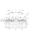
サーマルヘッド1は、図2に示すように、発熱抵抗体7および電極8が、矩形状の支持基板3の長手方向に複数配列されている。矢印Yは、紙送り機構17による感熱紙12の送り方向を示している。また、支持基板3の表面には、支持基板3の長手方向に延びる矩形状の凹部2が形成されている。ここで、符号Lr,Lm,Lc,Leはそれぞれ、後述する発熱部7Aの幅方向の寸法、凸部20の幅方向の寸法、凹部2の幅方向の寸法、薄肉部18の長手方向の寸法を示している。
As shown in FIG. 2, the thermal head 1 includes a plurality of
図2のA−A矢視断面図が、図3に示されている。
サーマルヘッド1は、図3に示すように、支持基板3と、支持基板3の上端面(表面)に接合された上板基板5と、上板基板5上に設けられた発熱抵抗体7と、発熱抵抗体7の両側に設けられた一対の電極8と、発熱抵抗体7および電極8を覆い、これらを磨耗や腐食から保護する保護膜9とを有している。
A cross-sectional view taken along line AA in FIG. 2 is shown in FIG.
As shown in FIG. 3, the thermal head 1 includes a
支持基板3は、例えば、300μm〜1mm程度の厚さを有するガラス基板やシリコン基板等の絶縁性の基板である。支持基板3の上端面(表面)、すなわち上板基板5との境界面には、支持基板3の長手方向に延びる矩形状の凹部2が形成されている。この凹部2は、例えば、深さ1μm〜100μm、幅50μm〜300μm程度の溝である。
The
上板基板5は、例えば、厚さ10μm〜100μm±5μm程度のガラス材質によって構成されており、発熱抵抗体7から発生した熱を蓄える蓄熱層として機能する。この上板基板5は、凹部2を密閉するように支持基板3の表面に積層状態に接合されている。上板基板5によって凹部2が覆われることにより、上板基板5と支持基板3との間には空洞部4が形成されている。
The
空洞部4は、全ての発熱抵抗体7に対向する連通構造を有しており、発熱抵抗体7から発生した熱が、上板基板5から支持基板3へ伝わることを抑制する中空断熱層として機能する。空洞部4を中空断熱層として機能させることで、発熱抵抗体7の下方の上板基板5を介して支持基板3に伝わる熱量よりも、発熱抵抗体7の上方へ伝わって印字等に利用される熱量を大きくすることができ、サーマルヘッド1の熱効率の向上することができる。
The
発熱抵抗体7は、上板基板5の上端面において、それぞれ凹部2を幅方向に跨ぐように設けられ、図2に示すように、凹部2の長手方向に所定の間隔をあけて複数配列されている。すなわち、各発熱抵抗体7は、上板基板5を介して空洞部4に対向して設けられ、空洞部4上に位置するように配置されている。
The
一対の電極8は、発熱抵抗体7に電流を供給して発熱させるためのものであり、各発熱抵抗体7の配列方向に直交する方向の一端に接続される共通電極8Aと、各発熱抵抗体7の他端に接続される個別電極8Bとから構成されている。図2に示すように、共通電極8Aは、全ての発熱抵抗体7に一体的に接続され、個別電極8Bは個々の発熱抵抗体7にそれぞれ接続されている。
The pair of
個別電極8Bに選択的に電圧を印加すると、選択された個別電極8Bとこれに対向する共通電極8Aとが接続されている発熱抵抗体7に電流が流れ、発熱抵抗体7が発熱するようになっている。この状態で、加圧機構19の作動により、発熱抵抗体7の発熱部分を覆う保護膜9の表面部分(印字部分)に感熱紙12を押し付けることで、感熱紙12が発色して印字されるようになっている。
When a voltage is selectively applied to the
なお、各発熱抵抗体7のうち実際に発熱する部分(図3に示す発熱部7A)は、発熱抵抗体7に電極8A,8Bが重なっていない部分、すなわち、発熱抵抗体7のうち共通電極8Aの接続面と個別電極8Bの接続面との間の領域であって、空洞部4のほぼ真上に位置する部分である。
Note that the part of each
また、一対の電極8A,8Bは、図2に示すように、発熱部7Aにおける発熱抵抗体7の長手方向に延びる長さ(ヒータ長)Lrが、隣接する発熱抵抗体7どうしの中心位置間の距離(ドット間距離あるいはドットピッチ)Wdより短くなるように配置することが望ましい。
Further, as shown in FIG. 2, the pair of
また、各電極8A,8Bは、図3に示すように、発熱抵抗体7の表面上に配置される接続部分に、他の領域(後述する厚肉部16)よりも厚さが薄い薄肉部18を有している。すなわち、電極8A,8Bは、上板基板5上に配置される部分と発熱抵抗体7上に配置される接続部分の一部が厚肉に形成され、発熱抵抗体7上の接続部分の残りが薄肉に形成されている。
Further, as shown in FIG. 3, each
厚肉部16は、例えば、1〜3μmの膜厚te1を有している。厚肉部16の膜厚te1は、電気抵抗値を十分に確保することができる程度、例えば、発熱抵抗体7の電気抵抗値に対して1/10以下程度にすることが望ましい。
The
薄肉部18は、発熱抵抗体7上における凹部2に対応する領域の内側から外側にわたって形成されている。薄肉部18の膜厚te2は、例えば50〜300nm程度であり、厚肉部16の膜厚te1および熱伝導率(Alの熱伝導率は約200W/(m・℃))と、上板基板5の厚さおよび熱伝導率(一般的なガラスの熱伝導率は約1W/(m・℃))とを考慮して設計される。
The
薄肉部18の膜厚te2を厚肉部16の膜厚te1より小さくすることにより、電極8A,8Bの熱伝導率が部分的に小さくなり、断熱効率が向上する。しかしながら、薄肉部18の膜厚te2が小さすぎると(例えば、薄肉部18の膜厚te2<10nm)、電極8A,8Bの電気抵抗値が部分的に大きくなるため、薄肉部18での電力ロスが断熱効率の向上分を超えてしまう。また、薄肉部18の膜厚te2は、スパッタ等で薄膜として得られる厚さであることも考慮する必要がある。そこで、薄肉部18の膜厚te2は、例えば、50〜300nm程度とすることが望ましい。
By making the film thickness te2 of the
また、各薄肉部18における発熱抵抗体7の長手方向に延びる長さLeを長くすることにより、電極8A,8Bの熱伝導率が部分的に小さくなり、断熱効率が向上する。しかしながら、薄肉部18の長さLeが長すぎると、電極8A,8Bの電気抵抗値が部分的に大きくなるため、薄肉部18での電力ロスが断熱効率の向上分を超えてしまう。したがって、各薄肉部18の電気抵抗値が、発熱部7Aの電気抵抗値の1/10以下となるように、薄肉部18の長さLeを決定することが望ましい。
Further, by increasing the length Le extending in the longitudinal direction of the
また、薄肉部18は、プラテンローラ4とヘッド部分9Aとが感熱紙3を挟んで接触する範囲の幅(ニップ幅)内に配置されていることが望ましい。ニップ幅はプラテンローラ4の直径や材質によって変化するが、一般的には、図3に示すように、ニップ幅は発熱抵抗体7の長手方向の長さLと一致すると考えられる。例えば、電極8Aの薄肉部18から電極8Bの薄肉部18までの幅寸法(Lr+2Le)は、約2mm以内(発熱部7Aの中心位置から約1mm以内)とする。また、発熱抵抗体7上の厚肉部16もニップ幅内に配置する。
Further, it is desirable that the
このような形状の電極8A,8Bは、発熱抵抗体7上に厚肉部16の一部と薄肉部18の全体が配置される二段構造となっている。電極8A,8Bにおける発熱抵抗体7と上板基板5との段差部分に配置される領域を厚肉(厚肉部16)にすることで、段差による電極8A,8Bの断切れおよび異常な電気抵抗値の上昇を防ぎ、断熱効率の向上およびサーマルヘッド10の信頼性の向上を図ることができる。
The
上板基板5には、図3に示すように、発熱抵抗体7が設けられる上面(表面)において、共通電極8Aと個別電極8Bとの間に凸部20が形成されている。凸部20は、平坦な先端面21と、先端面21の両端において先端面21に向かって漸次先細となるように傾斜して形成された側面22とを有している。すなわち、凸部20は、先端面21の幅方向の寸法が、凸部20の幅方向の寸法Lmよりも小さく形成されており、台形の縦断面形状を有している。
As shown in FIG. 3, the
また、凸部20は、その幅方向の寸法Lmが、凹部2の幅方向の寸法Lcよりも小さく形成されている。すなわち、凸部20は、上板基板5の上端側(表面)において、支持基板3に形成された凹部2に対応する領域内に形成されている。なお、凸部20の高さhmは、例えば0.5μm〜3μm程度であり、電極8の厚さ以上の高さに形成されている。
Further, the
ここで、比較例として、従来のサーマルヘッド100の構成について以下に説明する。
従来のサーマルヘッド100は、図10に示すように、上板基板50の上端側(表面)に凸部が設けられていないため、発熱抵抗体7と電極8との間に電極8の厚さ分だけ段差が生じる。これにより、発熱抵抗体7および電極8の上に形成された保護膜9の表面においても、上記の段差に対応する位置(図10に示す領域A)に段差が生じる。
Here, as a comparative example, the configuration of a conventional
As shown in FIG. 10, the conventional
その結果、プラテンローラ13により感熱紙12をサーマルヘッド100表面に押し付けた際、発熱抵抗体7と電極8との段差によって、感熱紙12とサーマルヘッド100表面の間に空気層101が生じる。この空気層101は、発熱抵抗体7により発生させた熱を感熱紙12へ伝達する際の妨げとなり、サーマルヘッド100の熱効率を低下させてしまうという不都合がある。
As a result, when the
これに対して、本実施形態に係るサーマルヘッド1によれば、図3に示すように、表面に凹部2が形成された支持基板3と上板基板5とが積層状態に接合されることで、支持基板3と上板基板5との間に空洞部4が形成される。この空洞部4は、発熱抵抗体7に対応する領域に形成されており、発熱抵抗体7から発生した熱を遮断する断熱層として機能する。したがって、本実施形態に係るサーマルヘッド1によれば、発熱抵抗体7から発生した熱が、上板基板5を介して支持基板3へ伝わって放散してしまうことを抑制することができ、発熱抵抗体7から発生した熱の利用率、すなわちサーマルヘッド1の熱効率を向上することができる。
On the other hand, according to the thermal head 1 according to the present embodiment, as shown in FIG. 3, the
さらに、上板基板5の電極8側の表面において、発熱抵抗体7の両側の一対の電極8の間に形成された凸部20により、凸部20の表面上に形成された発熱抵抗体7と、発熱抵抗体7の両端に設けられた電極8との段差を小さくすることができ、発熱抵抗体7(保護膜9)表面と感熱紙との間の空気層を小さくすることができる。したがって、本実施形態に係るサーマルヘッド1によれば、発熱抵抗体7により発生させた熱を感熱紙12に効率的に伝達することができ、サーマルヘッド1の熱効率を向上して印刷に必要なエネルギー量を低減することができる。
Further, on the surface of the
特に、凸部20の高さを電極8の高さ以上とすることで、サーマルヘッド1表面と感熱紙12との間の空気層を無くすことができ、サーマルヘッド1表面と感熱紙12とを密着させることができる。これにより、発熱抵抗体7により発生させた熱を感熱紙12に効率的に伝達することができ、サーマルヘッド1の熱効率を向上して印刷に必要なエネルギー量を低減することができる。
In particular, by setting the height of the
ここで、発熱抵抗体7において発生した熱は、電極8を介して上板基板5の平面方向へも拡散する。本実施形態に係るサーマルヘッド1は、空洞部4上に配置される電極8の薄肉部18において、電極8の他の領域(厚肉部16)よりも熱伝導率が低くなる。したがって、空洞部4(凹部2)に対応する領域内において薄肉部18を設けることで、発熱抵抗体7からの熱を空洞部4に対応する領域より外側に伝わり難くすることができる。これにより、空洞部4により支持基板3側への伝熱を抑制された熱に対して、電極8を介する上板基板5の平面方向への拡散を抑制し、支持基板3側とは反対側に伝熱させて印字効率の向上を図ることができる。
Here, the heat generated in the
次に、従来のサーマルヘッド100と本実施形態に係るサーマルヘッド1との強度の違いについて以下に説明する。
図4および図11は、強度の違いを説明するために、サーマルヘッドの上板基板と支持基板のみを簡略化して示した図であり、図4は本実施形態に係るサーマルヘッド1、図11は従来のサーマルヘッド100を示している。
Next, the difference in strength between the conventional
FIGS. 4 and 11 are simplified views showing only the upper substrate and the supporting substrate of the thermal head in order to explain the difference in strength. FIG. 4 shows the thermal head 1 and FIG. Shows a conventional
図11(a)に示すように、従来のサーマルヘッド100は、上板基板5の上端側(表面)が平坦な形状とされている。このような従来のサーマルヘッド100において、図11(b)に示すように、上板基板50の空洞部4上に集中荷重(矢印51)が加えられると、上板基板50の空洞部4に対向する部分は、下側に沈み込むように変形する。これにより、図11(b)の矢印52に示すように、上板基板50の下端面(裏面)、特に荷重のかかる中心位置において大きな引張応力が発生する。この場合、図11(c)に示すように、荷重位置Sと最大応力位置Tがほぼ一致することとなり、上板基板50が破損しやすくなる。
As shown in FIG. 11A, the conventional
これに対して、本実施形態に係るサーマルヘッド1は、図4(a)に示すように、上板基板5の上端側(表面)に凸部20が形成されている。このような構造とすることで、図4(b)に示すように、上板基板5の空洞部4上に集中荷重(矢印51)を加えた場合に、上板基板50の下端面(裏面)において、荷重のかかる中心位置および凸部20の麓部分に大きな引張応力が発生する(矢印31,32,33)。したがって、図4(c)に示すように、大きな応力がかかる位置は、領域T1,T2,T3に分散される。
On the other hand, as shown in FIG. 4A, the thermal head 1 according to the present embodiment has a
以上のように、本実施形態に係るサーマルヘッド1によれば、図11(a)に示すような均一な厚さの上板基板50に比べ、上板基板5の空洞部4(凹部2)に対応する位置(凸部20)が厚いため、上板基板5の強度を向上させることができる。また、上板基板5表面に集中荷重がかかった際、上板基板5表面にかかる引張応力を分散させることができる。その結果、例えばプラテンローラ13と感熱紙12との間に数μm〜数十μmの微小な異物が混入して上板基板5に集中荷重がかかった場合にも、割れにくく、信頼性の高いサーマルヘッド1を提供できる。
As described above, according to the thermal head 1 according to the present embodiment, the cavity 4 (recess 2) of the
ここで、サーマルヘッド1の保護膜9に使用される材料は、非常に内部応力が大きい。例えば、スパッタ法で成膜されたSiAlONは500〜2000MPaの内部応力を有する。そのため、空洞部4(凹部2)の直上において、上板基板5表面に凸部20を設けて上板基板5の板厚を増やすことで、上板基板5の強度を向上させ、保護膜9の内部応力による上板基板5の変形や破壊を防ぐことができる。
Here, the material used for the
また、本実施形態に係るサーマルヘッド1では、薄肉部18を含む電極8を凸部20の外側に配置している。このようにすることで、電極8の薄肉部18が凸部20の段差を乗り越えることがなく、さらに、薄肉部18にプラテンローラからの圧力がかかることを防止できるため、サーマルヘッドとしての信頼性を向上することができる。
Further, in the thermal head 1 according to the present embodiment, the
また、凸部20が上板基板5の表面と略平行な先端面21を有することで、プラテンローラ13の荷重を凸部20の先端面21全体で受けることができ、凸部20の一部に集中荷重が発生してしまうことを防止することができる。
Moreover, since the
したがって、上記のようなサーマルヘッド1を備えたサーマルプリンタ10によれば、上板基板5の強度を確保しつつ、サーマルヘッド1の熱効率を向上して印刷に必要なエネルギー量を低減することができる。これにより、少ない電力で感熱紙12に印刷することができ、バッテリーの持続時間を長期化させることができる。また、上板基板5の破損による故障を防止して装置としての信頼性を向上させることができる。
Therefore, according to the
[第1の変形例]
以下に、本実施形態に係るサーマルヘッド1の第1の変形例について説明する。なお、以降では、前述した第1の実施形態に係るサーマルヘッド1と共通する点については説明を省略し、異なる点について主に説明する。
[First Modification]
Below, the 1st modification of the thermal head 1 which concerns on this embodiment is demonstrated. In the following, description of points common to the above-described thermal head 1 according to the first embodiment will be omitted, and different points will be mainly described.
第1の実施形態に係るサーマルヘッド1では、図3に示すように、電極8の薄肉部18は、発熱抵抗体7上における凹部2に対応する領域の内側から外側にわたって配置されている。これに対して、本変形例に係るサーマルヘッド41では、図5に示すように、電極8の薄肉部18は、発熱抵抗体7上における凹部2に対応する領域の内側に形成されている。すなわち、本変形例に係るサーマルヘッド41では、発熱抵抗体7上における凹部2に対応する領域の内側にも厚肉部16が形成されている。
このように構成することで、電極8の厚肉部16を介した放熱量は大きくなるものの、電極8の電気抵抗値を小さくして発熱抵抗体7の発熱効率を向上することができる。
In the thermal head 1 according to the first embodiment, as shown in FIG. 3, the
With this configuration, although the amount of heat radiation through the
[第2の変形例]
以下に、本実施形態に係るサーマルヘッド1の第2の変形例について説明する。
第1の実施形態に係るサーマルヘッド1では、図3に示すように、電極8は、薄肉部18と厚肉部16とから構成される2段構造で形成されている。これに対して、本変形例に係るサーマルヘッド42では、図6に示すように、発熱抵抗体7近傍の電極8は、薄肉部18と中肉部17と厚肉部16とから構成される3段構造で構成されている。
[Second Modification]
Below, the 2nd modification of the thermal head 1 which concerns on this embodiment is demonstrated.
In the thermal head 1 according to the first embodiment, as shown in FIG. 3, the
このように構成することで、電極8の厚肉部16を介した放熱量と電極8の電気抵抗値(発熱抵抗体7の発熱効率)とのバランスを考慮して、サーマルヘッド全体の熱効率の最適化を図ることができる。また、中肉部17を設けることで、電極8の段差を小さくすることができ、電極8への保護膜9の成膜状態を向上させて電極8と保護膜9との剥離を防止することができる。
なお、本変形例において、電極8を3段構造で構成したが、4段以上で構成することとしてもよい。
With this configuration, considering the balance between the amount of heat radiation through the
In the present modification, the
[第3の変形例]
以下に、本実施形態に係るサーマルヘッド1の第3の変形例について説明する。
第1の実施形態に係るサーマルヘッド1では、前述のように、電極8は、薄肉部18と厚肉部16とから構成される2段構造で形成されている。これに対して、本変形例に係るサーマルヘッド43では、図7に示すように、発熱抵抗体7近傍の電極8は、内側から外側に従って厚くなるように形成されたテーパ部25を有している。
[Third Modification]
Below, the 3rd modification of the thermal head 1 which concerns on this embodiment is demonstrated.
In the thermal head 1 according to the first embodiment, as described above, the
このように構成することで、第1の実施形態に係るサーマルヘッド1と同様に、電極8を介して凹部2(空洞部4)に対応する領域から外側に拡散する熱量を低減するとともに、電極8の電気抵抗値を小さくして発熱抵抗体7の発熱効率の向上を図ることができる。また、電極8への保護膜9の成膜状態を向上することができ、電極8と保護膜9との剥離を防止することができる。
With this configuration, similarly to the thermal head 1 according to the first embodiment, the amount of heat diffused outward from the region corresponding to the recess 2 (cavity portion 4) via the
[第2の実施形態]
次に、本発明の第2の実施形態として、前述した第1の実施形態に係るサーマルヘッド1の製造方法について以下に説明する。
本実施形態に係るサーマルヘッド1の製造方法は、図8(a)から図8(h)に示すように、支持基板3の表面に開口部(凹部2)を形成する開口部形成工程と、凹部2が形成された支持基板3の表面に上板基板5の裏面を積層状態に接合する接合工程と、支持基板3に接合された上板基板5を薄板化する薄板化工程と、支持基板3に接合された上板基板5の表面に凸部20を形成する凸部形成工程と、上板基板5の表面において空洞部4に対応する領域に発熱抵抗体7を形成する抵抗体形成工程と、発熱抵抗体7の両端に電極8を形成する電極層形成工程と、電極8の上に保護膜9を形成する保護膜形成工程とを備えている。以下、上記の各工程について具体的に説明する。
[Second Embodiment]
Next, as a second embodiment of the present invention, a method for manufacturing the thermal head 1 according to the first embodiment will be described below.
As shown in FIGS. 8A to 8H, the method of manufacturing the thermal head 1 according to this embodiment includes an opening forming step of forming an opening (recess 2) on the surface of the
開口部形成工程では、図8(a)に示すように、支持基板3の上端面(表面)において、上板基板5の発熱抵抗体7を設ける領域に対応する位置に凹部2を形成する。凹部2は、例えば、支持基板3の表面に、サンドブラスト、ドライエッチング、ウェットエッチング、レーザ加工等を施すことによって形成する。
In the opening forming step, as shown in FIG. 8A, the
支持基板3にサンドブラストによる加工を施す場合には、支持基板3の表面にフォトレジスト材を被覆し、フォトレジスト材を所定パターンのフォトマスクを用いて露光して、凹部2を形成する領域以外の部分を固化させる。その後、支持基板3の表面を洗浄して固化していないフォトレジスト材を除去することで、凹部2を形成する領域にエッチング窓が形成されたエッチングマスク(図示略)が得られる。この状態で、支持基板3の表面にサンドブラストを施し、1〜100μmの深さの凹部2を形成する。凹部2の深さは、例えば、10μm以上で、支持基板3の厚さの半分以下とするのが好ましい。
When the
また、ドライエッチングやウェットエッチング等のエッチングによる加工を施す場合には、上記サンドブラストによる加工と同様に、支持基板3の表面の凹部2を形成する領域にエッチング窓が形成されたエッチングマスクを形成する。そして、この状態で支持基板3の表面にエッチングを施すことで、1〜100μmの深さの凹部2を形成する。
When processing by etching such as dry etching or wet etching is performed, an etching mask in which an etching window is formed in a region where the
このエッチング処理には、例えば、フッ酸系のエッチング液等を用いたウェットエッチングのほか、リアクティブイオンエッチング(RIE)やプラズマエッチング等のドライエッチングが用いられる。なお、参考例として、支持基板が単結晶シリコンの場合には、水酸化テトラメチルアンモニウム溶液、KOH溶液、または、フッ酸と硝酸の混合液等のエッチング液等によるウェットエッチングが行われる。 For this etching process, for example, dry etching such as reactive ion etching (RIE) or plasma etching is used in addition to wet etching using a hydrofluoric acid-based etching solution or the like. As a reference example, when the supporting substrate is single crystal silicon, wet etching is performed using an etching solution such as a tetramethylammonium hydroxide solution, a KOH solution, or a mixed solution of hydrofluoric acid and nitric acid.
次に、接合工程では、図8(b)に示すように、例えば厚さ約500〜700μmのガラス基板である上板基板5の下端面(裏面)と、凹部2が形成された支持基板3の上端面(表面)とを、高温融着や陽極接合によって接合する。この際、支持基板3と上板基板5とは乾燥状態で接合され、この接合された接合基板は、例えば200℃以上軟化点以下の温度で熱処理が行われる。
支持基板3と上板基板5とを接合することで、支持基板3に形成された凹部2が上板基板5によって覆われ、支持基板3と上板基板5との間に空洞部4が形成される。
Next, in the bonding step, as shown in FIG. 8B, for example, a lower substrate (back surface) of the
By bonding the
ここで、上板基板として100μm以下の厚さのものは、製造やハンドリングが困難であり、また、高価である。そこで、当初から薄い上板基板5を直接支持基板3に接合する代わりに、接合工程において製造やハンドリングが容易な厚さの上板基板5を支持基板3に接合した後、薄板化工程において上板基板5を所望の厚さに加工する。
Here, an upper substrate having a thickness of 100 μm or less is difficult to manufacture and handle, and is expensive. Therefore, instead of directly bonding the thin
次に、薄板化工程では、図8(c)に示すように、上板基板5の上端面(表面)側を、機械研磨することで薄板加工を行うことで、上板基板5を例えば約1〜100μmの厚さに加工する。なお、薄板化加工は、ドライエッチングやウェットエッチング等を施すことによって行うこととしてもよい。
Next, in the thinning step, as shown in FIG. 8C, the
次に、凸部形成工程では、図8(d)に示すように、ドライエッチングやウェットエッチング等を施すことによって、上板基板5の上端面(表面)において支持基板3に形成された凹部2に対応する領域に、凸部20を形成する。なお、この凸部形成工程は、薄板化工程と同時に行うこととしてもよい。すなわち、前述の薄板化工程において、凸部20を形成する領域をレジスト材で被覆し、ドライエッチングやウェットエッチング等によって、上板基板5の薄板化と同時に凸部20を形成することとしてもよい。
Next, in the convex portion forming step, as shown in FIG. 8D, the
次に、上板基板5上に発熱抵抗体7、共通電極8A、個別電極8B、および、保護膜9が順次形成される。
具体的には、抵抗体形成工程では、図8(e)に示すように、スパッタリングやCVD(化学気相成長法)、または、蒸着等の薄膜形成法を用いて上板基板5上にTa系やシリサイド系等の発熱抵抗体材料の薄膜を成膜する。発熱抵抗体材料の薄膜をリフトオフ法やエッチング法等を用いて成形することにより、所望の形状の発熱抵抗体7が形成される。
Next, the
Specifically, in the resistor forming step, as shown in FIG. 8E, Ta is formed on the
次に、電極層形成工程では、図8(f)に示すように、電極8の厚肉部16の下層(以下、第1層16aという。)を形成する第1層形成工程と、図8(g)に示すように、第1層16aの上から第2層16bを形成する第2層形成工程とを含んでいる。
Next, in the electrode layer forming step, as shown in FIG. 8F, a first layer forming step for forming a lower layer (hereinafter referred to as a
第1形成工程では、図8(f)に示すように、発熱抵抗体7の両端部における、空洞部4に対応する領域の外側において第1層16aを形成する。第1層16aは、スパッタリングや蒸着法等によりAl、Al−Si、Au、Ag、CuまたはPt等の配線材料を成膜し、この膜をリフトオフ法やエッチング法を用いたり、配線材料をスクリーン印刷した後に焼成したりすることにより、所望の形状に形成される。その厚みは、電極8配線での電力ロスを考慮し、例えば1〜3μm程度である。
In the first forming step, as shown in FIG. 8 (f), the
続いて、第2層形成工程では、図8(g)に示すように、発熱抵抗体7の両端部における空洞部4に対応する領域の内側から外側にわたって、ほぼ均等な厚さで第2層16bを形成する。第2層16bは、スパッタリングや蒸着法等により第1層16aと同じ材料を成膜し、この膜をリフトオフ法やエッチング法を用いたり、配線材料をスクリーン印刷した後に焼成したりすることにより、所望のパターンに形成される。
Subsequently, in the second layer forming step, as shown in FIG. 8G, the second layer is formed with a substantially uniform thickness from the inside to the outside of the region corresponding to the
第1層16aの表面と発熱抵抗体7の表面とにそれぞれ均等な厚さの第2層16bを形成することで、第2層16bで形成された薄肉部18と、薄肉部18よりも第1層16aの分だけ厚さが厚い厚肉部16とを有する2段構造の電極8を形成することができる。
このように形成する薄肉部18(第2層16b)の厚さは、厚肉部16の厚さ、熱伝導率(Alは約200W/(m・℃))、上板基板5の厚さ、熱伝導率(一般的なガラスは約1W/(m・℃))を考慮し、例えば50〜300nm程度とすることが望ましい。
By forming the
The thickness of the thin portion 18 (
次に、保護膜形成工程では、図8(h)に示すように、上板基板5上にSiO2、Ta2O5、SiAlON、Si3N4、ダイヤモンドライクカーボン等の保護膜材料をスパッタリング、イオンプレーティング、CVD法等により成膜して、保護膜9を形成する。これにより、図3に示されるサーマルヘッド1が製造される。
Next, in the protective film formation step, as shown in FIG. 8H, a protective film material such as SiO 2 , Ta 2 O 5 , SiAlON, Si 3 N 4 , diamond-like carbon, etc. is sputtered on the
このようなサーマルヘッド1の製造方法によれば、支持基板3と上板基板5との間に空洞部4が形成されるとともに、発熱抵抗体7の両端に形成された電極層の間に凸部20が形成されたサーマルヘッド1を製造することができる。また、発熱抵抗体の両端に、凹部2に対応する領域内において発熱抵抗体7に接続される薄肉部18と、発熱抵抗体7に接続され薄肉部18よりも厚く形成された厚肉部16とを有する電極層を形成することができる。これにより、上述のように、上板基板5の強度を確保しつつ、サーマルヘッド1の熱効率を向上して印刷に必要なエネルギー量を低減することができる。
According to such a method of manufacturing the thermal head 1, the
[変形例]
以下に、本実施形態に係るサーマルヘッド1の製造方法の変形例について説明する。
本変形例に係るサーマルヘッド1の製造方法が、前述した第2の実施形態に係るサーマルヘッド1の製造方法と異なる点は、電極8の薄肉部18と厚肉部16の形成方法である。以降では、第2の実施形態に係るサーマルヘッド1の製造方法と共通する点については説明を省略し、異なる点について主に説明する。
[Modification]
Below, the modification of the manufacturing method of the thermal head 1 which concerns on this embodiment is demonstrated.
The manufacturing method of the thermal head 1 according to this modification differs from the manufacturing method of the thermal head 1 according to the second embodiment described above in the method of forming the
前述の第2の実施形態に係るサーマルヘッド1の製造方法では、第1層形成工程および第2層形成工程により電極8を2段構造に形成したが、本変形例に係るサーマルヘッド1の製造方法では、エッチング法により電極8を2段構造に形成する。
具体的には、本変形例に係るサーマルヘッド1の製造方法において、電極層形成工程は、図9(f)に示すように、厚肉部16以上の厚さで厚肉電極層26を形成する厚肉電極層形成工程と、図9(g)に示すように、厚肉電極層26の一部を除去する電極層除去工程とを含んでいる。
In the manufacturing method of the thermal head 1 according to the second embodiment described above, the
Specifically, in the method of manufacturing the thermal head 1 according to the present modification, the electrode layer forming step forms the
厚肉電極層形成工程では、図9(f)に示すように、発熱抵抗体7の両端部における空洞部4に対応する領域の内側から外側にわたって、ほぼ均等な厚さで、且つ、厚肉部16以上の厚さで厚肉電極層26を形成する。厚肉電極層26は、Al、Al−Si、Au、Ag、Cu、Pt等の配線材料をスパッタリングや蒸着法等により成膜する。そして、この膜をリフトオフ法やエッチング法を用いて形成したり、配線材料をスクリーン印刷した後に焼成したりするなどして、所望の形状の電極8のパターンを形成する。
In the thick electrode layer forming step, as shown in FIG. 9 (f), the both ends of the
電極層除去工程では、図9(g)に示すように、厚肉電極層26の空洞部4に対応する領域の内側および外側の一部(薄肉部18を形成する領域)をエッチングにより除去する。これにより、厚肉部16と、厚肉部16よりもエッチングにより除去された分だけ厚さが薄い薄肉部18とを有する2段構造の電極8を形成することができる。
In the electrode layer removing step, as shown in FIG. 9G, a part of the inner side and the outer side of the
以上のように、本変形に係るサーマルヘッド1の製造方法によれば、前述の第2の実施形態に係るサーマルヘッド1の製造方法と同様の効果に加えて、電極8の第1層16aと第2層16bとの界面を無くすことができ、電極8の強度および電気伝導度を向上することができる。
As described above, according to the method for manufacturing the thermal head 1 according to this modification, in addition to the same effects as the method for manufacturing the thermal head 1 according to the second embodiment described above, the
以上、本発明の各実施形態について図面を参照して詳述してきたが、具体的な構成はこの実施形態に限られるものではなく、本発明の要旨を逸脱しない範囲の設計変更等も含まれる。
例えば、本発明を各実施形態および各変形例を適宜組み合わせた実施形態に適用してもよく、特に限定されるものではない。
また、凸部20は、台形の縦断面形状を有していることとして説明したが、本発明の参考例としての発明の参考実施形態においては、凸部は、発熱抵抗体7を形成することができればよく、例えば矩形等の縦断面形状や曲面形状としてもよい。
As mentioned above, although each embodiment of the present invention has been described in detail with reference to the drawings, the specific configuration is not limited to this embodiment, and includes design changes and the like without departing from the gist of the present invention. .
For example, the present invention may be applied to embodiments in which each embodiment and each modified example are appropriately combined, and are not particularly limited.
Moreover, although the
また、支持基板3の長手方向に延びる矩形状の凹部2を形成し、空洞部4が全ての発熱抵抗体7に対向する連通構造を有することとしたが、これに代えて、支持基板3の長手方向に沿って、発熱抵抗体7に対向する位置にそれぞれ独立した凹部2を形成することとし、上板基板5によって凹部2ごとに独立した空洞部4が形成されることとしてもよい。これにより、複数の独立した中空断熱層を備えるサーマルヘッドを形成することができる。
また、一対の電極8の両方に厚肉部16および薄肉部18を設けることとして説明したが、一対の電極8の一方のみに厚肉部16および薄肉部18を設けることとしてもよい。
In addition, the rectangular
In addition, although the
1,41,42,43 サーマルヘッド
2 凹部
3 支持基板
4 空洞部
5 上板基板
7 発熱抵抗体
8 電極
9 保護膜
10 サーマルプリンタ(プリンタ)
16 厚肉部
17 中肉部
18 薄肉部
20 凸部
21 先端面
22 側面
25 テーパ部
26 厚肉電極層
1, 41, 42, 43
16
Claims (5)
該支持基板の表面に積層状態に接合され、前記凹部に対応する領域内に凸部が形成された上板基板と、
該上板基板の表面において前記凸部を跨ぐ位置に設けられた発熱抵抗体と、
該発熱抵抗体の両側に設けられた一対の電極とを備え、
前記凸部が、平坦な先端面と、該先端面の両端に該先端面に向かって漸次先細となるように傾斜して形成された側面とを有し、
前記一対の電極の少なくとも一方が、
前記凹部に対応する領域内において前記発熱抵抗体に接続される薄肉部と、
前記発熱抵抗体に接続され前記薄肉部よりも厚く形成された厚肉部とを有し、
前記一対の電極が、前記凸部よりも外側の領域に形成されているサーマルヘッド。 A support substrate having a recess on the surface;
An upper substrate that is bonded to the surface of the support substrate in a laminated state and has a convex portion formed in a region corresponding to the concave portion;
A heating resistor provided at a position across the convex portion on the surface of the upper substrate;
A pair of electrodes provided on both sides of the heating resistor,
The convex portion has a flat tip surface and side surfaces formed so as to be gradually tapered toward the tip surface at both ends of the tip surface,
At least one of the pair of electrodes is
A thin portion connected to the heating resistor in a region corresponding to the recess;
A thick portion connected to the heating resistor and formed thicker than the thin portion;
A thermal head in which the pair of electrodes are formed in a region outside the convex portion.
該サーマルヘッドの前記発熱抵抗体に感熱記録媒体を押し付けながら送り出す加圧機構とを備えるプリンタ。 The thermal head according to any one of claims 1 to 3 ,
A printer comprising: a pressurizing mechanism that sends out a thermal recording medium while pressing the thermal recording medium against the heating resistor of the thermal head.
該開口部形成工程により前記開口部が形成された前記支持基板の表面に上板基板の裏面を積層状態に接合する接合工程と、
該接合工程により前記支持基板に接合された前記上板基板を薄板化する薄板化工程と、
前記接合工程により前記支持基板に接合された前記上板基板の表面の前記開口部に対応する領域内に、平坦な先端面および該先端面の両端に該先端面に向かって漸次先細となるように傾斜した側面を有する凸部を形成する凸部形成工程と、
前記上板基板の表面において、前記開口部に対応する領域に発熱抵抗体を形成する抵抗体形成工程と、
該抵抗体形成工程により形成された発熱抵抗体の両端に、前記開口部に対応する領域内において前記発熱抵抗体に接続される薄肉部と、前記発熱抵抗体に接続され前記薄肉部よりも厚く形成された厚肉部とを有する電極層を、前記凸部よりも外側の領域に配されるように形成する電極層形成工程とを備えるサーマルヘッドの製造方法。 An opening forming step of forming an opening on the surface of the support substrate;
A bonding step of bonding the back surface of the upper substrate to the surface of the support substrate on which the opening is formed by the opening forming step;
A thinning step of thinning the upper substrate bonded to the support substrate by the bonding step;
In the region corresponding to the opening on the surface of the upper substrate bonded to the support substrate by the bonding step , a flat front end surface and both ends of the front end surface are gradually tapered toward the front end surface. A protrusion forming step of forming a protrusion having a side surface inclined to
A resistor forming step of forming a heating resistor in a region corresponding to the opening on the surface of the upper substrate;
At both ends of the heating resistor formed by the resistor forming step, a thin portion connected to the heating resistor in a region corresponding to the opening , and a thicker portion connected to the heating resistor than the thin portion. A method of manufacturing a thermal head comprising: an electrode layer forming step of forming an electrode layer having a formed thick portion so as to be disposed in a region outside the convex portion.
Priority Applications (4)
| Application Number | Priority Date | Filing Date | Title |
|---|---|---|---|
| JP2011037310A JP5765844B2 (en) | 2011-02-23 | 2011-02-23 | Thermal head, manufacturing method thereof, and printer |
| EP12155066.9A EP2492101B1 (en) | 2011-02-23 | 2012-02-13 | Thermal Head and Method of Manufacturing the same, and Printer |
| CN201210040855.8A CN102649368B (en) | 2011-02-23 | 2012-02-21 | Hot head and manufacture method thereof and printer |
| US13/401,894 US8629892B2 (en) | 2011-02-23 | 2012-02-22 | Thermal head, method of manufacturing thermal head, and printer equipped with thermal head |
Applications Claiming Priority (1)
| Application Number | Priority Date | Filing Date | Title |
|---|---|---|---|
| JP2011037310A JP5765844B2 (en) | 2011-02-23 | 2011-02-23 | Thermal head, manufacturing method thereof, and printer |
Publications (3)
| Publication Number | Publication Date |
|---|---|
| JP2012171288A JP2012171288A (en) | 2012-09-10 |
| JP2012171288A5 JP2012171288A5 (en) | 2014-01-30 |
| JP5765844B2 true JP5765844B2 (en) | 2015-08-19 |
Family
ID=45607043
Family Applications (1)
| Application Number | Title | Priority Date | Filing Date |
|---|---|---|---|
| JP2011037310A Active JP5765844B2 (en) | 2011-02-23 | 2011-02-23 | Thermal head, manufacturing method thereof, and printer |
Country Status (4)
| Country | Link |
|---|---|
| US (1) | US8629892B2 (en) |
| EP (1) | EP2492101B1 (en) |
| JP (1) | JP5765844B2 (en) |
| CN (1) | CN102649368B (en) |
Families Citing this family (2)
| Publication number | Priority date | Publication date | Assignee | Title |
|---|---|---|---|---|
| JP2013082092A (en) * | 2011-10-06 | 2013-05-09 | Seiko Instruments Inc | Thermal head and method of manufacturing the same, and thermal printer |
| JP5943414B2 (en) * | 2011-12-01 | 2016-07-05 | セイコーインスツル株式会社 | Manufacturing method of thermal head |
Family Cites Families (20)
| Publication number | Priority date | Publication date | Assignee | Title |
|---|---|---|---|---|
| JPS5420745A (en) * | 1977-07-15 | 1979-02-16 | Nec Corp | Thermal head |
| JPS606478A (en) * | 1983-06-24 | 1985-01-14 | Hitachi Ltd | Thermal recording head |
| JPS61290067A (en) * | 1985-06-19 | 1986-12-20 | Hitachi Ltd | Thermal head |
| JPH01221259A (en) * | 1988-02-29 | 1989-09-04 | Nikon Corp | Substrate for thermal head |
| JPH04147869A (en) * | 1990-10-11 | 1992-05-21 | Alps Electric Co Ltd | Thermal head |
| KR920009583A (en) * | 1990-11-20 | 1992-06-25 | 정용문 | Method of manufacturing the thermal recording element |
| JP3241755B2 (en) * | 1991-07-23 | 2001-12-25 | ローム株式会社 | Thermal head and electronic device using the same |
| JP3231951B2 (en) * | 1994-05-12 | 2001-11-26 | アルプス電気株式会社 | Thermal head and method of manufacturing the same |
| US5594488A (en) * | 1994-05-12 | 1997-01-14 | Alps Electric Co., Ltd. | Thermal head |
| JP2002036614A (en) * | 2000-07-25 | 2002-02-06 | Seiko Instruments Inc | Thin film thermal head |
| JP2002067367A (en) * | 2000-08-31 | 2002-03-05 | Alps Electric Co Ltd | Thermal head and its manufacturing method |
| JP4895344B2 (en) * | 2005-09-22 | 2012-03-14 | セイコーインスツル株式会社 | Heating resistance element, thermal head and printer using the same |
| JP5039940B2 (en) * | 2005-10-25 | 2012-10-03 | セイコーインスツル株式会社 | Heating resistance element, thermal head, printer, and method of manufacturing heating resistance element |
| JP2007245666A (en) * | 2006-03-17 | 2007-09-27 | Sony Corp | Thermal head and printer apparatus |
| JP4548370B2 (en) * | 2006-03-17 | 2010-09-22 | ソニー株式会社 | Thermal head and printer device |
| JP2007245667A (en) * | 2006-03-17 | 2007-09-27 | Sony Corp | Thermal head and printer |
| JP2009119850A (en) | 2007-10-23 | 2009-06-04 | Seiko Instruments Inc | Heating resistor element, manufacturing method for the same, thermal head, and printer |
| US7768541B2 (en) * | 2007-10-23 | 2010-08-03 | Seiko Instruments Inc. | Heating resistor element, manufacturing method for the same, thermal head, and printer |
| JP5408695B2 (en) * | 2008-10-27 | 2014-02-05 | セイコーインスツル株式会社 | Manufacturing method of thermal head |
| JP5672479B2 (en) * | 2010-08-25 | 2015-02-18 | セイコーインスツル株式会社 | Thermal head, printer, and thermal head manufacturing method |
-
2011
- 2011-02-23 JP JP2011037310A patent/JP5765844B2/en active Active
-
2012
- 2012-02-13 EP EP12155066.9A patent/EP2492101B1/en not_active Not-in-force
- 2012-02-21 CN CN201210040855.8A patent/CN102649368B/en not_active Expired - Fee Related
- 2012-02-22 US US13/401,894 patent/US8629892B2/en not_active Expired - Fee Related
Also Published As
| Publication number | Publication date |
|---|---|
| EP2492101A1 (en) | 2012-08-29 |
| CN102649368B (en) | 2015-11-18 |
| CN102649368A (en) | 2012-08-29 |
| US20120212558A1 (en) | 2012-08-23 |
| JP2012171288A (en) | 2012-09-10 |
| EP2492101B1 (en) | 2014-10-08 |
| US8629892B2 (en) | 2014-01-14 |
Similar Documents
| Publication | Publication Date | Title |
|---|---|---|
| JP5408695B2 (en) | Manufacturing method of thermal head | |
| JP5200256B2 (en) | Manufacturing method of thermal head | |
| JP5421680B2 (en) | Thermal head manufacturing method, thermal head and printer | |
| JP2007320197A (en) | Thermal head, manufacturing method of thermal head, and printer | |
| US8111273B2 (en) | Thermal head, printer, and manufacturing method for thermal head | |
| EP2298562B1 (en) | Thermal head and printer | |
| US20110216147A1 (en) | Thermal head, printer, and manufacturing method for the thermal head | |
| JP5765845B2 (en) | Thermal head, manufacturing method thereof, and printer | |
| JP5477741B2 (en) | Thermal head, manufacturing method thereof, and printer | |
| JP5311336B2 (en) | Thermal head, thermal printer and thermal head manufacturing method | |
| US8477166B2 (en) | Thermal head, thermal printer and manufacturing method for the thermal head | |
| JP5765844B2 (en) | Thermal head, manufacturing method thereof, and printer | |
| JP5273786B2 (en) | Thermal head, printer, and thermal head manufacturing method | |
| JP5794727B2 (en) | Thermal head and printer | |
| JP5181328B2 (en) | Heating resistance element parts and thermal printer | |
| JP5311335B2 (en) | Manufacturing method of thermal head |
Legal Events
| Date | Code | Title | Description |
|---|---|---|---|
| A521 | Request for written amendment filed |
Free format text: JAPANESE INTERMEDIATE CODE: A523 Effective date: 20131210 |
|
| A621 | Written request for application examination |
Free format text: JAPANESE INTERMEDIATE CODE: A621 Effective date: 20131210 |
|
| A977 | Report on retrieval |
Free format text: JAPANESE INTERMEDIATE CODE: A971007 Effective date: 20140917 |
|
| A131 | Notification of reasons for refusal |
Free format text: JAPANESE INTERMEDIATE CODE: A131 Effective date: 20141104 |
|
| A521 | Request for written amendment filed |
Free format text: JAPANESE INTERMEDIATE CODE: A523 Effective date: 20141222 |
|
| TRDD | Decision of grant or rejection written | ||
| A01 | Written decision to grant a patent or to grant a registration (utility model) |
Free format text: JAPANESE INTERMEDIATE CODE: A01 Effective date: 20150602 |
|
| RD03 | Notification of appointment of power of attorney |
Free format text: JAPANESE INTERMEDIATE CODE: A7423 Effective date: 20150615 |
|
| A61 | First payment of annual fees (during grant procedure) |
Free format text: JAPANESE INTERMEDIATE CODE: A61 Effective date: 20150615 |
|
| R150 | Certificate of patent or registration of utility model |
Ref document number: 5765844 Country of ref document: JP Free format text: JAPANESE INTERMEDIATE CODE: R150 |
|
| R250 | Receipt of annual fees |
Free format text: JAPANESE INTERMEDIATE CODE: R250 |
|
| R250 | Receipt of annual fees |
Free format text: JAPANESE INTERMEDIATE CODE: R250 |
|
| R250 | Receipt of annual fees |
Free format text: JAPANESE INTERMEDIATE CODE: R250 |
|
| R250 | Receipt of annual fees |
Free format text: JAPANESE INTERMEDIATE CODE: R250 |
|
| R250 | Receipt of annual fees |
Free format text: JAPANESE INTERMEDIATE CODE: R250 |
|
| R250 | Receipt of annual fees |
Free format text: JAPANESE INTERMEDIATE CODE: R250 |