EP2421044A1 - Edge Termination Region for Semiconductor Device - Google Patents
Edge Termination Region for Semiconductor Device Download PDFInfo
- Publication number
- EP2421044A1 EP2421044A1 EP10172933A EP10172933A EP2421044A1 EP 2421044 A1 EP2421044 A1 EP 2421044A1 EP 10172933 A EP10172933 A EP 10172933A EP 10172933 A EP10172933 A EP 10172933A EP 2421044 A1 EP2421044 A1 EP 2421044A1
- Authority
- EP
- European Patent Office
- Prior art keywords
- region
- gate
- isolation
- edge
- fingers
- Prior art date
- Legal status (The legal status is an assumption and is not a legal conclusion. Google has not performed a legal analysis and makes no representation as to the accuracy of the status listed.)
- Granted
Links
Images


Classifications
-
- H—ELECTRICITY
- H10—SEMICONDUCTOR DEVICES; ELECTRIC SOLID-STATE DEVICES NOT OTHERWISE PROVIDED FOR
- H10D—INORGANIC ELECTRIC SEMICONDUCTOR DEVICES
- H10D30/00—Field-effect transistors [FET]
- H10D30/60—Insulated-gate field-effect transistors [IGFET]
- H10D30/64—Double-diffused metal-oxide semiconductor [DMOS] FETs
- H10D30/66—Vertical DMOS [VDMOS] FETs
- H10D30/668—Vertical DMOS [VDMOS] FETs having trench gate electrodes, e.g. UMOS transistors
-
- H—ELECTRICITY
- H10—SEMICONDUCTOR DEVICES; ELECTRIC SOLID-STATE DEVICES NOT OTHERWISE PROVIDED FOR
- H10D—INORGANIC ELECTRIC SEMICONDUCTOR DEVICES
- H10D30/00—Field-effect transistors [FET]
- H10D30/60—Insulated-gate field-effect transistors [IGFET]
- H10D30/64—Double-diffused metal-oxide semiconductor [DMOS] FETs
- H10D30/66—Vertical DMOS [VDMOS] FETs
- H10D30/665—Vertical DMOS [VDMOS] FETs having edge termination structures
-
- H—ELECTRICITY
- H10—SEMICONDUCTOR DEVICES; ELECTRIC SOLID-STATE DEVICES NOT OTHERWISE PROVIDED FOR
- H10D—INORGANIC ELECTRIC SEMICONDUCTOR DEVICES
- H10D64/00—Electrodes of devices having potential barriers
- H10D64/111—Field plates
- H10D64/117—Recessed field plates, e.g. trench field plates or buried field plates
-
- H—ELECTRICITY
- H10—SEMICONDUCTOR DEVICES; ELECTRIC SOLID-STATE DEVICES NOT OTHERWISE PROVIDED FOR
- H10D—INORGANIC ELECTRIC SEMICONDUCTOR DEVICES
- H10D64/00—Electrodes of devices having potential barriers
- H10D64/20—Electrodes characterised by their shapes, relative sizes or dispositions
- H10D64/27—Electrodes not carrying the current to be rectified, amplified, oscillated or switched, e.g. gates
- H10D64/311—Gate electrodes for field-effect devices
- H10D64/411—Gate electrodes for field-effect devices for FETs
- H10D64/511—Gate electrodes for field-effect devices for FETs for IGFETs
- H10D64/517—Gate electrodes for field-effect devices for FETs for IGFETs characterised by the conducting layers
- H10D64/519—Gate electrodes for field-effect devices for FETs for IGFETs characterised by the conducting layers characterised by their top-view geometrical layouts
Definitions
- the invention relates to an edge termination region for a semiconductor device and a method of making it.
- a number of approaches are used to process the edges of semiconductor devices.
- the intention is to avoid breakdown of the semiconductor device as a result of edge effects.
- the inventors have sought to efficiently provide a RESURF structure in the edge termination region to increase the breakdown voltage of the device compared with an arrangement without the RESURF structure.
- a convenient step to carry out the integration is after the mask step known as contact opening, i.e. after deposition of insulator (such as tetraethylorthosilicate, TEOS) and the creation of openings in the insulator.
- insulator such as tetraethylorthosilicate, TEOS
- lon implantation may be carried out at this point using the insulator to create a plurality of pillars to act as a RESURF structure to protect the remainder of the semiconductor device.
- the problem with this approach is of course that the implantation can only take place in regions where there is an opening in the insulator. This is fine in the active region, but is not easy to implement in the edge termination region.
- the solution adopted by the inventors is to use a different RESURF effect in the intermediate region, namely by incorporating isolation fingers in this region on both sides of the gate trenches.
- the gate trenches are used to connect the edge gate trenches with the gate of the semiconductor device in the central active region.
- a further factor is that to save silicon area, and indeed one mask, it is convenient to deposit gate metal over the edge region of the semiconductor device and to connect the gate metal to edge gate conductor in trenches in this region. In this case, the gate metal can give rise to significant gate-drain capacitance which can seriously impact the performance of the device.
- the invention relates to a method of making the semiconductor device as taught in claim 11.
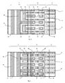
- Figure 1 shows a top view of a semiconductor device according to the first embodiment at a stage of manufacture before the deposition of the gate and source metallisations, though Figure 1 does show as dotted lines the relevant zones in which these metallisations are deposited, and Figure 2 a side view of the semiconductor device at this stage.
- Figure 3 shows the situation after the deposition of the gate and source metallisations.
- the semiconductor device includes an edge termination region 2 and a central region 4.
- the left edge of Figure 1 is the edge of the semiconductor device
- the right edge of Figure 1 is the central region which includes in this embodiment a high voltage semiconductor device.
- the direction from top to bottom in Figure 1 is a circumferential direction, around the circumference of the device, while the direction from left to right is a radial direction, from the edge towards the central region 4.
- the central region 4 of the semiconductor device includes gate trenches 6, which alternate with semiconductor body regions 8.
- the gate trenches are shown with vertical lines. In the example, the depth of the gate trenches is 0.4 ⁇ m to 1.2 ⁇ m, in some cases up to 1.8 ⁇ m.
- the gate trenches include insulated sidewalls and are filled with a conductive gate.
- a source region 52 is provided as well as a drain region 60, the latter being constituted by the substrate.
- the gates in the gate trenches 6 control the vertical conduction between source 52 and drain 60 as is known in the art.
- an insulator layer 54 in the example of TEOS, is deposited and various contact regions defined by a single mask.
- a source contact region 10 is defined at the top of the semiconductor body regions 8 to provide a source contact.
- a source metal 12 is provided over this region ( Figure 3 ), providing an electrical contact to the source contact regions.
- the semiconductor device thus contains a vertical high voltage field effect transistor in the central region 4, the source 52 being at the top and the drain 60 being the substrate, the high voltage field effect transistor in this instance made up of a single field effect transistor arranged as a repeating cell with a device cell pitch, in the example 1.7 ⁇ m.
- central region there are other types of device that can be formed in the central region.
- lateral field effect transistors may also be formed.
- the central region may also include an integrated circuit with multiple components.
- the edge termination formed in edge termination region 2 is formed in a way that does not require too many additional masks or processes.
- the edge termination includes deep trenches 20,34 extending in the example for a depth of 1.0 ⁇ m to 8.0 ⁇ m, in the example 2 ⁇ m.
- An isolation region 14 is formed between the edge termination region 2 and the central region 4.
- the isolation region 14 comprises isolation fingers 22, 24 extending in the radial direction.
- the gate trenches 6 include in particular edge gate trenches 28 in the edge termination region and gate contacts 30 defined in the edge gate trenches.
- the gate contacts 30 are defined in the same way and the same process as the source contacts 10.
- Gate fingers 18 alternating with the isolation fingers 22,24 connect the edge gate trenches 28 to the gate trenches 6 in the central region 4.
- a gate metal 32 extends over the edge termination region and provides the electrical connection to the gate contacts 30 and hence to the edge gate trenches 28 and via the gate fingers 18 to the gate trenches 6. In this way, the edge termination region 2 is used for the gate connection therefore avoiding the need for a separate region to connect to the gates.
- the isolation fingers include first isolation fingers 22 extending from the deep trenches 20 inwards from those trenches past the edge gate trenches 28, and second isolation fingers 24 which are not connected to the deep trenches 20 but which extend in alignment with the edge gate trenches 28 from inwards of the edge gate trenches 28 towards the central region 4. Note that the deep trenches 20, first isolation fingers 22 and second isolation fingers 24 are formed in a single process.
- the deep trenches 20,34 and first and second isolation fingers 22,24 have a thick sidewall of oxide and are filled with conductive polysilicon. This may be p-type or n-type, but conveniently is doped highly enough so that the polysilicon functions effectively as a conductor.
- Trench contacts 26 are defined over the isolation fingers 22, 24 - these are formed in the same process as source contacts 10 and gate contacts 30.
- the trench contacts 26 connect to the source metal 12 which accordingly overlaps not merely the source contacts 10 in the central region 4 but also overlaps the isolation region 14 to arrange that the deep trenches 20 and isolation fingers 22,24 are connected to the source. Note that it is the first isolation fingers 22 which are in connection with deep trenches 20 that provide the source connection to these deep trenches 20. It will also be noted that there is an outer deep trench 34 that is not connected to the source - this does not cause problems.
- the capacitance of the edge gate trenches in the edge region is shielded from the device by the reduced surface field effect in the isolation region 14.
- the manufacture of the device in the central region 4 is relatively standard and so will not be described in full detail.
- the formation of vertical field effect transistors with gate trenches 6, body 8, and source and drain 52,60 is known.
- the source 52 is formed by an implanted region of higher n-type carrier density than body 8. This is patterned using source-n mask having source-n mask edge 50 ( Fig. 1 ) so that the source 52 does not reach the outer edge of the source contact 10. This mask ensures that the source 52 is not present in the edge termination region, where it may create a parasitic npn transistor which may cause failure if high avalanche currents flow.
- the source-n mask is eliminated and the source 52 implantation carried out over the whole surface of the semiconductor device, relying on the improved breakdown achieved by the structure.
- the same mask and process steps are used to form the edge gate trenches 28 and the gate fingers 18 as described above and as illustrated in Figure 1 .
- An isolation definition mask is used to form the deep trenches 20, 34 of the deep trench isolation structure and the fingers 22,24 in a single operation. In principle, this step may take place before or after the manufacture of the gate trenches.
- TEOS layer 54 is deposited over the whole structure and contact openings 30,26,10 formed.
- p-type pillars 56 are deposited through the source contact openings 10 in the central region 4. These provide the RESURF effect in the central region 4.
- the p-type pillars are thus aligned with the source contact openings 10. Note that the structure of the semiconductor device of source, body and drain is maintained adjacent to the gate trenches 6 since the source contact openings 10 do not extend as far as the gate trenches. Thus, the function of the semiconductor device is maintained.
- a moat etch is then performed (not shown) through the same openings 30,26,10, which is relatively shallow compared with the deep trenches. Then, a metal layer is deposited and a further mask used to pattern this layer to form gate metal 32 and source metal 12, the former in connection with gate contact 30 and the latter in connection with source contact 10 and trench contact 26.
- the moat etch means that the metal layer contacts the polysilicon not just at the surface but also at the sides of the moat, which can act to improve the connection of the gate metal 32 and source metal 12. If this improvement is not required, the moat etch also can be omitted.
- edge cell pitch in the region of the edge gate trenches 28 and the isolation fingers 22, 24 is not the same as the device cell pitch in the central region 4.
- the pitch of the edge gate trenches is considerably larger, This allows enough space for the shielding isolation fingers 22, 24.
- the gate trenches 6 of the device in the central region are connected to gate metal 32 at the edge gate trenches 28 which are wider than the gate trenches elsewhere in the structure. This makes for improved connection to the gate.
- the structure includes floating intermediate semiconductor regions 36. In many examples, this will not cause a problem since the area is quite small and the regions are bounded by deep trenches, the isolation fingers 22,24.
- the isolation fingers 22, 24 are each broken into two, namely an outer region 44, an inner region 46, and a bridge 42 between the outer region and the inner region.
- Source contacts 47 are provided in each of the outer region 44, the inner region 46 and the bridge to connect each of these to the source metal 12.
- the bridge 42 provides the source connection of the semiconductor in the isolation regions.
- FIG. 6 A further variation is shown in Figure 6 .
- the first and second isolation fingers 22,24 are replaced by a single set of isolation fingers 22 that simply alternate with the edge gate trenches 28.
- the edge gate trenches are oriented to extend towards the central region 4 rather than to extend circumferentially as in the embodiments of Figures 1 to 3 .
- isolation fingers 22, 24 are connected to the source, but in alternative embodiments these may be left floating.
- metal in the terms “source metal” and “gate metal” is not intended to exclude metallic, conductive arrangements that are not strictly speaking pure metal.
Landscapes
- Insulated Gate Type Field-Effect Transistor (AREA)
- Electrodes Of Semiconductors (AREA)
Abstract
Description
- The invention relates to an edge termination region for a semiconductor device and a method of making it.
- A number of approaches are used to process the edges of semiconductor devices. In general, the intention is to avoid breakdown of the semiconductor device as a result of edge effects.
- A prior approach to edge termination, using what is known as a "reduced surface field" effect, is taught in
US 2010/0001362 . "Reduced surface field" is often abbreviated to RESURF. - According to the invention, there is provided a semiconductor device with an edge termination region according to claim 1.
- The inventors have sought to efficiently provide a RESURF structure in the edge termination region to increase the breakdown voltage of the device compared with an arrangement without the RESURF structure.
- One approach to such a RESURF structure is taught in
US 2010/0001362 , as mentioned above. This uses pillars to achieve a suitable structure. - When integrating such pillars into a conventional process, a convenient step to carry out the integration is after the mask step known as contact opening, i.e. after deposition of insulator (such as tetraethylorthosilicate, TEOS) and the creation of openings in the insulator. lon implantation may be carried out at this point using the insulator to create a plurality of pillars to act as a RESURF structure to protect the remainder of the semiconductor device. The problem with this approach is of course that the implantation can only take place in regions where there is an opening in the insulator. This is fine in the active region, but is not easy to implement in the edge termination region. In particular, there needs to be a gap between the gate metal and the source metal for isolation purposes and in this gap it is not possible to put a contact. Pillars may accordingly not be provided in this gap, which has the result that the breakdown may occur at lower voltage in this region.
- To solve this problem, the solution adopted by the inventors is to use a different RESURF effect in the intermediate region, namely by incorporating isolation fingers in this region on both sides of the gate trenches. The gate trenches are used to connect the edge gate trenches with the gate of the semiconductor device in the central active region.
- A further factor is that to save silicon area, and indeed one mask, it is convenient to deposit gate metal over the edge region of the semiconductor device and to connect the gate metal to edge gate conductor in trenches in this region. In this case, the gate metal can give rise to significant gate-drain capacitance which can seriously impact the performance of the device.
- By providing the isolation fingers alternating with the gate fingers, it is possible to achieve a "reduced surface field" ("RESURF") effect in this region. This can improve capacitance effects, in particular reduced gate-drain capacitance.
- In another aspect, the invention relates to a method of making the semiconductor device as taught in claim 11.
- For a better understanding of the invention, embodiments will now be described, purely by way of example, with reference to the accompanying drawings, in which:
-
Figure 1 shows a first embodiment of the invention in top view; -
Figure 2 shows a stage in the manufacture of the first embodiment of the invention in side section along line A-A inFigure 1 ; -
Figure 3 shows a later stage in the manufacture of the first embodiment of the invention in side section along line A-A inFigure 1 ; -
Figure 4 shows a second embodiment of the invention; -
Figure 5 shows a third embodiment of the invention; and -
Figure 6 shows a fourth embodiment of the invention. - The same reference numbers are used for the same or corresponding features in the various figures and the description relating to these features is not necessarily repeated. The figures are schematic and not to scale.
- Referring to
Figures 1 to 3 ,Figure 1 shows a top view of a semiconductor device according to the first embodiment at a stage of manufacture before the deposition of the gate and source metallisations, thoughFigure 1 does show as dotted lines the relevant zones in which these metallisations are deposited, andFigure 2 a side view of the semiconductor device at this stage.Figure 3 shows the situation after the deposition of the gate and source metallisations. - The semiconductor device includes an
edge termination region 2 and a central region 4. Thus, the left edge ofFigure 1 is the edge of the semiconductor device, the right edge ofFigure 1 is the central region which includes in this embodiment a high voltage semiconductor device. Thus, the direction from top to bottom inFigure 1 is a circumferential direction, around the circumference of the device, while the direction from left to right is a radial direction, from the edge towards the central region 4. - The central region 4 of the semiconductor device includes
gate trenches 6, which alternate withsemiconductor body regions 8. The gate trenches are shown with vertical lines. In the example, the depth of the gate trenches is 0.4 µm to 1.2 µm, in some cases up to 1.8 µm. The gate trenches include insulated sidewalls and are filled with a conductive gate. Asource region 52 is provided as well as adrain region 60, the latter being constituted by the substrate. The gates in the gate trenches 6 control the vertical conduction betweensource 52 anddrain 60 as is known in the art. - After forming various components in the semiconductor body, an
insulator layer 54, in the example of TEOS, is deposited and various contact regions defined by a single mask. In the central region 4, asource contact region 10 is defined at the top of thesemiconductor body regions 8 to provide a source contact. - A
source metal 12 is provided over this region (Figure 3 ), providing an electrical contact to the source contact regions. The semiconductor device thus contains a vertical high voltage field effect transistor in the central region 4, thesource 52 being at the top and thedrain 60 being the substrate, the high voltage field effect transistor in this instance made up of a single field effect transistor arranged as a repeating cell with a device cell pitch, in the example 1.7 µm. - Those skilled in the art will appreciate that there are other types of device that can be formed in the central region. For example, lateral field effect transistors may also be formed. The central region may also include an integrated circuit with multiple components.
- The edge termination formed in
edge termination region 2 is formed in a way that does not require too many additional masks or processes. The edge termination includesdeep trenches - An
isolation region 14 is formed between theedge termination region 2 and the central region 4. Theisolation region 14 comprisesisolation fingers -
Intermediate semiconductor regions 36 remain separating theisolation fingers gate fingers 18. - The
gate trenches 6 include in particularedge gate trenches 28 in the edge termination region andgate contacts 30 defined in the edge gate trenches. Thegate contacts 30 are defined in the same way and the same process as thesource contacts 10.Gate fingers 18 alternating with theisolation fingers edge gate trenches 28 to thegate trenches 6 in the central region 4. - A
gate metal 32 extends over the edge termination region and provides the electrical connection to thegate contacts 30 and hence to theedge gate trenches 28 and via thegate fingers 18 to thegate trenches 6. In this way, theedge termination region 2 is used for the gate connection therefore avoiding the need for a separate region to connect to the gates. - The isolation fingers include
first isolation fingers 22 extending from thedeep trenches 20 inwards from those trenches past theedge gate trenches 28, andsecond isolation fingers 24 which are not connected to thedeep trenches 20 but which extend in alignment with theedge gate trenches 28 from inwards of theedge gate trenches 28 towards the central region 4. Note that thedeep trenches 20,first isolation fingers 22 andsecond isolation fingers 24 are formed in a single process. - The
deep trenches second isolation fingers -
Trench contacts 26 are defined over theisolation fingers 22, 24 - these are formed in the same process assource contacts 10 andgate contacts 30. Thetrench contacts 26 connect to thesource metal 12 which accordingly overlaps not merely thesource contacts 10 in the central region 4 but also overlaps theisolation region 14 to arrange that thedeep trenches 20 andisolation fingers first isolation fingers 22 which are in connection withdeep trenches 20 that provide the source connection to thesedeep trenches 20. It will also be noted that there is an outerdeep trench 34 that is not connected to the source - this does not cause problems. - By virtue of the source connected
isolation fingers edge gate trenches 28 and the central region 4 containing the active device the capacitance of the edge gate trenches in the edge region is shielded from the device by the reduced surface field effect in theisolation region 14. - To manufacture the device, the manufacture of the device in the central region 4 is relatively standard and so will not be described in full detail. In particular, the formation of vertical field effect transistors with
gate trenches 6,body 8, and source and drain 52,60 is known. - One aspect of the manufacture is worth pointing out. The
source 52 is formed by an implanted region of higher n-type carrier density thanbody 8. This is patterned using source-n mask having source-n mask edge 50 (Fig. 1 ) so that thesource 52 does not reach the outer edge of thesource contact 10. This mask ensures that thesource 52 is not present in the edge termination region, where it may create a parasitic npn transistor which may cause failure if high avalanche currents flow. - In alternative embodiments, the source-n mask is eliminated and the
source 52 implantation carried out over the whole surface of the semiconductor device, relying on the improved breakdown achieved by the structure. - During manufacture of the
gate trenches 6 in the active region, the same mask and process steps are used to form theedge gate trenches 28 and thegate fingers 18 as described above and as illustrated inFigure 1 . - An isolation definition mask is used to form the
deep trenches fingers - After the formation of the semiconductor body and structures in the body,
TEOS layer 54 is deposited over the whole structure andcontact openings type pillars 56 are deposited through thesource contact openings 10 in the central region 4. These provide the RESURF effect in the central region 4. The p-type pillars are thus aligned with thesource contact openings 10. Note that the structure of the semiconductor device of source, body and drain is maintained adjacent to thegate trenches 6 since thesource contact openings 10 do not extend as far as the gate trenches. Thus, the function of the semiconductor device is maintained. - A further etch, a moat etch is then performed (not shown) through the
same openings gate metal 32 andsource metal 12, the former in connection withgate contact 30 and the latter in connection withsource contact 10 andtrench contact 26. The moat etch means that the metal layer contacts the polysilicon not just at the surface but also at the sides of the moat, which can act to improve the connection of thegate metal 32 andsource metal 12. If this improvement is not required, the moat etch also can be omitted. - It should be noted that the Figures are not to scale - in fact the slight dips shown in the top of the metallisation layer of
Figure 3 can in real life be relatively deep trenches, with depths of order the width or depths double the width. These can be filled if required with tungsten plugs. - A number of other aspects of this arrangement are worth noting.
- Firstly, the edge cell pitch in the region of the
edge gate trenches 28 and theisolation fingers shielding isolation fingers - The
gate trenches 6 of the device in the central region are connected togate metal 32 at theedge gate trenches 28 which are wider than the gate trenches elsewhere in the structure. This makes for improved connection to the gate. - The structure includes floating
intermediate semiconductor regions 36. In many examples, this will not cause a problem since the area is quite small and the regions are bounded by deep trenches, theisolation fingers - However, a change in device structure in the alternative embodiment illustrated in
Figure 4 ensures that these intermediate semiconductor regions are not floating but are source connectedintermediate semiconductor regions 38. This is ensured bybridge 40 joining theintermediate semiconductor regions 38 to thesource regions 8 in the central region 4. - An alternative change to the device structure of
Figure 1 to achieve the same result is shown inFigure 5 . - In this case, the
isolation fingers outer region 44, aninner region 46, and abridge 42 between the outer region and the inner region.Source contacts 47 are provided in each of theouter region 44, theinner region 46 and the bridge to connect each of these to thesource metal 12. Thus in this embodiment thebridge 42 provides the source connection of the semiconductor in the isolation regions. - A further variation is shown in
Figure 6 . In this case, the first andsecond isolation fingers isolation fingers 22 that simply alternate with theedge gate trenches 28. In this case, the edge gate trenches are oriented to extend towards the central region 4 rather than to extend circumferentially as in the embodiments ofFigures 1 to 3 . - Further, in the example shown the
isolation fingers - Those skilled in the art will realise that modifications are possible. For example, the term "metal" in the terms "source metal" and "gate metal" is not intended to exclude metallic, conductive arrangements that are not strictly speaking pure metal.
Claims (13)
- A semiconductor device having an edge termination region, the device comprising:a central region (4) forming at least one field effect transistor with a semiconductor body (8) having a source (52), drain (60) and gate,an edge termination region (2) including at least one deep trench isolation region (20) and a plurality of edge gate trench regions (28), the edge gate trench regions (28) comprising an insulated gate in a trench; andan isolation region (14) between the edge termination region (2) and the central region (4), the isolation region comprising gate fingers (18) extending from the edge gate trench regions (28) to the gate trenches (6) in the central region (4) to electrically connect the edge gate trench regions to the gate trenches (6) in the central region, and the isolation region further comprising conductive isolation fingers (22,24) extending from the edge termination region (2) towards the central region (4) and gate between the gate fingers (18).
- A semiconductor device according to claim 1, wherein the source (52) is of first conductivity type, connected to a source metal (12) through a plurality of source contacts(10), the semiconductor device further comprising a region of second conductivity type extending into the semiconductor body from the source contacts to reduce the breakdown voltage in the central region (4).
- A semiconductor device according to claim 2 wherein the source metal (12) is further connected to trench contacts (26,47) on the isolation fingers (22,24) to connect the isolation fingers to the source.
- A semiconductor device according to any preceding claim, further comprising a gate metal (32) over the edge gate trench regions connected to the edge gate trench regions through a gate contact (30) on the edge gate trench regions to provide a gate connection to the semiconductor device.
- A semiconductor device according to any preceding claim wherein the central region (4) includes a plurality of source contacts at a source pitch, and the pitch of the plurality of edge gate trench regions (28) is greater than the source pitch.
- A semiconductor device according to any preceding claim, further comprising an n-well (58) in the edge termination region.
- A semiconductor device according to any preceding claim further comprising a gate metal (34) over the edge termination region (2) directly in contact with gate contacts (30) in the edge gate trench regions (28) to provide a gate connection to the semiconductor device.
- A semiconductor device according to any preceding claim, wherein the isolation fingers (22,24) include:a first set of isolation fingers (22) being extensions of the deep trench isolation regions (20), anda second set of isolation fingers (24) being separated from the deep trench isolation regions (20) by the edge gate trench regions (28) and alternating with the first set of isolation fingers.
- A semiconductor device according to any of claims 1 to 7, wherein the isolation fingers (22) are each extensions of the deep trench isolation regions (20) and
the isolation fingers (22) alternate with the edge gate trench regions (28). - A semiconductor device according to any preceding claim, wherein at least some of the isolation fingers have an outer region (44) being an extension of the deep trench isolation region (20), and an inner region (46) separated from the outer region by a finger semiconductor region (42) ,
further comprising a source contact (47) in each of the outer region (44), the finger semiconductor region (42) and the inner region (46) of at least some of the isolation fingers, the source contacts being connected to source metal (12). - A method of manufacturing a semiconductor device, comprising:(a) forming a central region (4) with at least one field effect transistor with a semiconductor body (8) of a first conductivity type, the field effect transistor having a source (52), drain (60) and gate,(b) forming an edge termination region (2) including at least one deep trench isolation region (20) and a plurality of edge gate trench regions (28), the edge gate trench regions (28) comprising an insulated gate in a trench;(c) forming an isolation region (14) between the edge termination region (2) and the central region (4), the isolation region comprising gate fingers (18) extending from the edge gate trench regions (28) to the gate in the central region (4) and the isolation region further comprising conductive isolation fingers (22,24) extending from the edge termination region (2) towards the central region (4) and gate between the gate fingers (18);
where steps (a), (b), and (c) can take place in any order and/or concurrently, the method further comprising:(d) depositing an insulating layer (52);(e) forming contact openings (47,30,26,10) in the insulating layer; and(f) implanting regions of a second conductivity type opposite to the first conductivity type through the contact openings for improving the breakdown voltage of the device. - A method according to claim 11 including implanting over the complete semiconductor device a region of first conductivity type of higher doping concentration than the semiconductor body to form the source (52) in the central region (4).
- A method according to claim 11 or 12 further comprising implanting a counter doping of second conductivity type in the edge termination region (2) to reduce the doping of first conductivity type at the surface of the semiconductor in the edge termination region (2).
Priority Applications (3)
| Application Number | Priority Date | Filing Date | Title |
|---|---|---|---|
| EP10172933.3A EP2421044B1 (en) | 2010-08-16 | 2010-08-16 | Edge Termination Region for Semiconductor Device |
| CN201110230833.3A CN102376750B (en) | 2010-08-16 | 2011-08-12 | Edge termination region |
| US13/210,308 US8513733B2 (en) | 2010-08-16 | 2011-08-15 | Edge termination region of a semiconductor device |
Applications Claiming Priority (1)
| Application Number | Priority Date | Filing Date | Title |
|---|---|---|---|
| EP10172933.3A EP2421044B1 (en) | 2010-08-16 | 2010-08-16 | Edge Termination Region for Semiconductor Device |
Publications (2)
| Publication Number | Publication Date |
|---|---|
| EP2421044A1 true EP2421044A1 (en) | 2012-02-22 |
| EP2421044B1 EP2421044B1 (en) | 2015-07-29 |
Family
ID=43568183
Family Applications (1)
| Application Number | Title | Priority Date | Filing Date |
|---|---|---|---|
| EP10172933.3A Active EP2421044B1 (en) | 2010-08-16 | 2010-08-16 | Edge Termination Region for Semiconductor Device |
Country Status (3)
| Country | Link |
|---|---|
| US (1) | US8513733B2 (en) |
| EP (1) | EP2421044B1 (en) |
| CN (1) | CN102376750B (en) |
Families Citing this family (7)
| Publication number | Priority date | Publication date | Assignee | Title |
|---|---|---|---|---|
| IT1401755B1 (en) | 2010-08-30 | 2013-08-02 | St Microelectronics Srl | INTEGRATED ELECTRONIC DEVICE WITH VERTICAL CONDUCTION AND ITS MANUFACTURING METHOD. |
| IT1401756B1 (en) * | 2010-08-30 | 2013-08-02 | St Microelectronics Srl | INTEGRATED ELECTRONIC DEVICE WITH ON-BOARD TERMINATION STRUCTURE AND ITS MANUFACTURING METHOD. |
| IT1401754B1 (en) | 2010-08-30 | 2013-08-02 | St Microelectronics Srl | INTEGRATED ELECTRONIC DEVICE AND ITS MANUFACTURING METHOD. |
| CN103928460B (en) * | 2014-04-21 | 2017-06-30 | 上海联星电子有限公司 | A kind of radio frequency LDMOS domain structure |
| US9589847B1 (en) * | 2016-02-18 | 2017-03-07 | International Business Machines Corporation | Metal layer tip to tip short |
| CN114429981A (en) * | 2022-01-06 | 2022-05-03 | 上海华虹宏力半导体制造有限公司 | Groove type power device |
| CN114429982A (en) * | 2022-01-06 | 2022-05-03 | 上海华虹宏力半导体制造有限公司 | Groove type power device |
Citations (7)
| Publication number | Priority date | Publication date | Assignee | Title |
|---|---|---|---|---|
| WO2000042665A1 (en) * | 1999-01-11 | 2000-07-20 | Fraunhofer-Gesellschaft zur Förderung der angewandten Forschung e.V. | Power mos element and method for producing the same |
| WO2001008226A2 (en) * | 1999-07-22 | 2001-02-01 | Koninklijke Philips Electronics N.V. | Cellular trench-gate field-effect transistors |
| US7186618B2 (en) * | 2003-10-30 | 2007-03-06 | Infineon Technologies Ag | Power transistor arrangement and method for fabricating it |
| US20090085105A1 (en) * | 2007-10-02 | 2009-04-02 | Shih Tzung Su | Trench mosfet and method of manufacture utilizing two masks |
| US20090127616A1 (en) * | 2007-11-07 | 2009-05-21 | Kabushiki Kaisha Toshiba | Power semiconductor device and method for manufacturing same |
| US20100001362A1 (en) | 2005-05-24 | 2010-01-07 | Nxp B.V. | Edge termination for semiconductor device |
| US20100072544A1 (en) * | 2008-09-24 | 2010-03-25 | Jeffrey Pearse | Method of forming an mos transistor and structure therefor |
-
2010
- 2010-08-16 EP EP10172933.3A patent/EP2421044B1/en active Active
-
2011
- 2011-08-12 CN CN201110230833.3A patent/CN102376750B/en active Active
- 2011-08-15 US US13/210,308 patent/US8513733B2/en active Active
Patent Citations (7)
| Publication number | Priority date | Publication date | Assignee | Title |
|---|---|---|---|---|
| WO2000042665A1 (en) * | 1999-01-11 | 2000-07-20 | Fraunhofer-Gesellschaft zur Förderung der angewandten Forschung e.V. | Power mos element and method for producing the same |
| WO2001008226A2 (en) * | 1999-07-22 | 2001-02-01 | Koninklijke Philips Electronics N.V. | Cellular trench-gate field-effect transistors |
| US7186618B2 (en) * | 2003-10-30 | 2007-03-06 | Infineon Technologies Ag | Power transistor arrangement and method for fabricating it |
| US20100001362A1 (en) | 2005-05-24 | 2010-01-07 | Nxp B.V. | Edge termination for semiconductor device |
| US20090085105A1 (en) * | 2007-10-02 | 2009-04-02 | Shih Tzung Su | Trench mosfet and method of manufacture utilizing two masks |
| US20090127616A1 (en) * | 2007-11-07 | 2009-05-21 | Kabushiki Kaisha Toshiba | Power semiconductor device and method for manufacturing same |
| US20100072544A1 (en) * | 2008-09-24 | 2010-03-25 | Jeffrey Pearse | Method of forming an mos transistor and structure therefor |
Also Published As
| Publication number | Publication date |
|---|---|
| US20120037980A1 (en) | 2012-02-16 |
| CN102376750B (en) | 2015-04-08 |
| CN102376750A (en) | 2012-03-14 |
| EP2421044B1 (en) | 2015-07-29 |
| US8513733B2 (en) | 2013-08-20 |
Similar Documents
| Publication | Publication Date | Title |
|---|---|---|
| TWI684276B (en) | Ditch-type power transistor and manufacturing method thereof | |
| US7655975B2 (en) | Power trench transistor | |
| US10861965B2 (en) | Power MOSFET with an integrated pseudo-Schottky diode in source contact trench | |
| US8294235B2 (en) | Edge termination with improved breakdown voltage | |
| JP5089284B2 (en) | Semiconductor device having a space-saving edge structure | |
| KR101213068B1 (en) | Semiconductor device and method for fabricating the same | |
| US9385188B2 (en) | Semiconductor device with termination region having floating electrodes in an insulating layer | |
| US8445958B2 (en) | Power semiconductor device with trench bottom polysilicon and fabrication method thereof | |
| US8513733B2 (en) | Edge termination region of a semiconductor device | |
| US20210242342A1 (en) | Semiconductor device and method for manufacturing same | |
| JP5136578B2 (en) | Semiconductor device | |
| JP6375176B2 (en) | Semiconductor device and manufacturing method of semiconductor device | |
| CN111081779A (en) | A shielded gate trench MOSFET and its manufacturing method | |
| JP2016127245A (en) | Semiconductor device and manufacturing method of semiconductor device | |
| US11532741B2 (en) | Semiconductor device having vertical DMOS and manufacturing method thereof | |
| US10141397B2 (en) | Semiconductor device and method of manufacturing the same | |
| CN111564493A (en) | Trench power transistor and method of making the same | |
| CN108511341B (en) | Shielded gate trench power device and method of making the same | |
| US9324800B1 (en) | Bidirectional MOSFET with suppressed bipolar snapback and method of manufacture | |
| US9954118B2 (en) | Method of producing a high-voltage semiconductor drift device | |
| KR20050030538A (en) | Semiconductor device and manufacturing method thereof | |
| KR20050009797A (en) | Structure of high voltage transistor with shallow trench isolation layer | |
| US20240429231A1 (en) | Semiconductor die with a vertical transistor device | |
| CN103515424A (en) | Semiconductor device and fabricating method thereof | |
| CN113889536B (en) | Shielded gate trench semiconductor structure and shielded gate trench semiconductor device |
Legal Events
| Date | Code | Title | Description |
|---|---|---|---|
| AK | Designated contracting states |
Kind code of ref document: A1 Designated state(s): AL AT BE BG CH CY CZ DE DK EE ES FI FR GB GR HR HU IE IS IT LI LT LU LV MC MK MT NL NO PL PT RO SE SI SK SM TR |
|
| AX | Request for extension of the european patent |
Extension state: BA ME RS |
|
| PUAI | Public reference made under article 153(3) epc to a published international application that has entered the european phase |
Free format text: ORIGINAL CODE: 0009012 |
|
| 17P | Request for examination filed |
Effective date: 20120822 |
|
| 17Q | First examination report despatched |
Effective date: 20130312 |
|
| GRAP | Despatch of communication of intention to grant a patent |
Free format text: ORIGINAL CODE: EPIDOSNIGR1 |
|
| INTG | Intention to grant announced |
Effective date: 20150213 |
|
| GRAS | Grant fee paid |
Free format text: ORIGINAL CODE: EPIDOSNIGR3 |
|
| GRAA | (expected) grant |
Free format text: ORIGINAL CODE: 0009210 |
|
| AK | Designated contracting states |
Kind code of ref document: B1 Designated state(s): AL AT BE BG CH CY CZ DE DK EE ES FI FR GB GR HR HU IE IS IT LI LT LU LV MC MK MT NL NO PL PT RO SE SI SK SM TR |
|
| REG | Reference to a national code |
Ref country code: GB Ref legal event code: FG4D |
|
| REG | Reference to a national code |
Ref country code: CH Ref legal event code: EP |
|
| REG | Reference to a national code |
Ref country code: AT Ref legal event code: REF Ref document number: 739893 Country of ref document: AT Kind code of ref document: T Effective date: 20150815 |
|
| REG | Reference to a national code |
Ref country code: IE Ref legal event code: FG4D |
|
| REG | Reference to a national code |
Ref country code: DE Ref legal event code: R096 Ref document number: 602010026171 Country of ref document: DE |
|
| REG | Reference to a national code |
Ref country code: AT Ref legal event code: MK05 Ref document number: 739893 Country of ref document: AT Kind code of ref document: T Effective date: 20150729 |
|
| REG | Reference to a national code |
Ref country code: LT Ref legal event code: MG4D |
|
| REG | Reference to a national code |
Ref country code: NL Ref legal event code: MP Effective date: 20150729 |
|
| PG25 | Lapsed in a contracting state [announced via postgrant information from national office to epo] |
Ref country code: GR Free format text: LAPSE BECAUSE OF FAILURE TO SUBMIT A TRANSLATION OF THE DESCRIPTION OR TO PAY THE FEE WITHIN THE PRESCRIBED TIME-LIMIT Effective date: 20151030 Ref country code: LV Free format text: LAPSE BECAUSE OF FAILURE TO SUBMIT A TRANSLATION OF THE DESCRIPTION OR TO PAY THE FEE WITHIN THE PRESCRIBED TIME-LIMIT Effective date: 20150729 Ref country code: NO Free format text: LAPSE BECAUSE OF FAILURE TO SUBMIT A TRANSLATION OF THE DESCRIPTION OR TO PAY THE FEE WITHIN THE PRESCRIBED TIME-LIMIT Effective date: 20151029 Ref country code: FI Free format text: LAPSE BECAUSE OF FAILURE TO SUBMIT A TRANSLATION OF THE DESCRIPTION OR TO PAY THE FEE WITHIN THE PRESCRIBED TIME-LIMIT Effective date: 20150729 Ref country code: LT Free format text: LAPSE BECAUSE OF FAILURE TO SUBMIT A TRANSLATION OF THE DESCRIPTION OR TO PAY THE FEE WITHIN THE PRESCRIBED TIME-LIMIT Effective date: 20150729 |
|
| PG25 | Lapsed in a contracting state [announced via postgrant information from national office to epo] |
Ref country code: PT Free format text: LAPSE BECAUSE OF FAILURE TO SUBMIT A TRANSLATION OF THE DESCRIPTION OR TO PAY THE FEE WITHIN THE PRESCRIBED TIME-LIMIT Effective date: 20151130 Ref country code: ES Free format text: LAPSE BECAUSE OF FAILURE TO SUBMIT A TRANSLATION OF THE DESCRIPTION OR TO PAY THE FEE WITHIN THE PRESCRIBED TIME-LIMIT Effective date: 20150729 Ref country code: SE Free format text: LAPSE BECAUSE OF FAILURE TO SUBMIT A TRANSLATION OF THE DESCRIPTION OR TO PAY THE FEE WITHIN THE PRESCRIBED TIME-LIMIT Effective date: 20150729 Ref country code: HR Free format text: LAPSE BECAUSE OF FAILURE TO SUBMIT A TRANSLATION OF THE DESCRIPTION OR TO PAY THE FEE WITHIN THE PRESCRIBED TIME-LIMIT Effective date: 20150729 Ref country code: IS Free format text: LAPSE BECAUSE OF FAILURE TO SUBMIT A TRANSLATION OF THE DESCRIPTION OR TO PAY THE FEE WITHIN THE PRESCRIBED TIME-LIMIT Effective date: 20151129 Ref country code: AT Free format text: LAPSE BECAUSE OF FAILURE TO SUBMIT A TRANSLATION OF THE DESCRIPTION OR TO PAY THE FEE WITHIN THE PRESCRIBED TIME-LIMIT Effective date: 20150729 Ref country code: PL Free format text: LAPSE BECAUSE OF FAILURE TO SUBMIT A TRANSLATION OF THE DESCRIPTION OR TO PAY THE FEE WITHIN THE PRESCRIBED TIME-LIMIT Effective date: 20150729 |
|
| PG25 | Lapsed in a contracting state [announced via postgrant information from national office to epo] |
Ref country code: NL Free format text: LAPSE BECAUSE OF FAILURE TO SUBMIT A TRANSLATION OF THE DESCRIPTION OR TO PAY THE FEE WITHIN THE PRESCRIBED TIME-LIMIT Effective date: 20150729 |
|
| REG | Reference to a national code |
Ref country code: CH Ref legal event code: PL |
|
| PG25 | Lapsed in a contracting state [announced via postgrant information from national office to epo] |
Ref country code: CZ Free format text: LAPSE BECAUSE OF FAILURE TO SUBMIT A TRANSLATION OF THE DESCRIPTION OR TO PAY THE FEE WITHIN THE PRESCRIBED TIME-LIMIT Effective date: 20150729 Ref country code: IT Free format text: LAPSE BECAUSE OF FAILURE TO SUBMIT A TRANSLATION OF THE DESCRIPTION OR TO PAY THE FEE WITHIN THE PRESCRIBED TIME-LIMIT Effective date: 20150729 Ref country code: MC Free format text: LAPSE BECAUSE OF FAILURE TO SUBMIT A TRANSLATION OF THE DESCRIPTION OR TO PAY THE FEE WITHIN THE PRESCRIBED TIME-LIMIT Effective date: 20150729 Ref country code: CH Free format text: LAPSE BECAUSE OF NON-PAYMENT OF DUE FEES Effective date: 20150831 Ref country code: EE Free format text: LAPSE BECAUSE OF FAILURE TO SUBMIT A TRANSLATION OF THE DESCRIPTION OR TO PAY THE FEE WITHIN THE PRESCRIBED TIME-LIMIT Effective date: 20150729 Ref country code: LI Free format text: LAPSE BECAUSE OF NON-PAYMENT OF DUE FEES Effective date: 20150831 Ref country code: SK Free format text: LAPSE BECAUSE OF FAILURE TO SUBMIT A TRANSLATION OF THE DESCRIPTION OR TO PAY THE FEE WITHIN THE PRESCRIBED TIME-LIMIT Effective date: 20150729 Ref country code: DK Free format text: LAPSE BECAUSE OF FAILURE TO SUBMIT A TRANSLATION OF THE DESCRIPTION OR TO PAY THE FEE WITHIN THE PRESCRIBED TIME-LIMIT Effective date: 20150729 |
|
| REG | Reference to a national code |
Ref country code: DE Ref legal event code: R097 Ref document number: 602010026171 Country of ref document: DE |
|
| PG25 | Lapsed in a contracting state [announced via postgrant information from national office to epo] |
Ref country code: RO Free format text: LAPSE BECAUSE OF FAILURE TO SUBMIT A TRANSLATION OF THE DESCRIPTION OR TO PAY THE FEE WITHIN THE PRESCRIBED TIME-LIMIT Effective date: 20150729 |
|
| REG | Reference to a national code |
Ref country code: IE Ref legal event code: MM4A |
|
| PLBE | No opposition filed within time limit |
Free format text: ORIGINAL CODE: 0009261 |
|
| STAA | Information on the status of an ep patent application or granted ep patent |
Free format text: STATUS: NO OPPOSITION FILED WITHIN TIME LIMIT |
|
| GBPC | Gb: european patent ceased through non-payment of renewal fee |
Effective date: 20151029 |
|
| 26N | No opposition filed |
Effective date: 20160502 |
|
| PG25 | Lapsed in a contracting state [announced via postgrant information from national office to epo] |
Ref country code: IE Free format text: LAPSE BECAUSE OF NON-PAYMENT OF DUE FEES Effective date: 20150816 Ref country code: GB Free format text: LAPSE BECAUSE OF NON-PAYMENT OF DUE FEES Effective date: 20151029 |
|
| PG25 | Lapsed in a contracting state [announced via postgrant information from national office to epo] |
Ref country code: SI Free format text: LAPSE BECAUSE OF FAILURE TO SUBMIT A TRANSLATION OF THE DESCRIPTION OR TO PAY THE FEE WITHIN THE PRESCRIBED TIME-LIMIT Effective date: 20150729 |
|
| REG | Reference to a national code |
Ref country code: DE Ref legal event code: R081 Ref document number: 602010026171 Country of ref document: DE Owner name: NEXPERIA B.V., NL Free format text: FORMER OWNER: NXP B.V., EINDHOVEN, NL |
|
| REG | Reference to a national code |
Ref country code: FR Ref legal event code: ST Effective date: 20160907 |
|
| PG25 | Lapsed in a contracting state [announced via postgrant information from national office to epo] |
Ref country code: FR Free format text: LAPSE BECAUSE OF NON-PAYMENT OF DUE FEES Effective date: 20150929 |
|
| PG25 | Lapsed in a contracting state [announced via postgrant information from national office to epo] |
Ref country code: MT Free format text: LAPSE BECAUSE OF FAILURE TO SUBMIT A TRANSLATION OF THE DESCRIPTION OR TO PAY THE FEE WITHIN THE PRESCRIBED TIME-LIMIT Effective date: 20150729 |
|
| PG25 | Lapsed in a contracting state [announced via postgrant information from national office to epo] |
Ref country code: BG Free format text: LAPSE BECAUSE OF FAILURE TO SUBMIT A TRANSLATION OF THE DESCRIPTION OR TO PAY THE FEE WITHIN THE PRESCRIBED TIME-LIMIT Effective date: 20150729 Ref country code: SM Free format text: LAPSE BECAUSE OF FAILURE TO SUBMIT A TRANSLATION OF THE DESCRIPTION OR TO PAY THE FEE WITHIN THE PRESCRIBED TIME-LIMIT Effective date: 20150729 Ref country code: HU Free format text: LAPSE BECAUSE OF FAILURE TO SUBMIT A TRANSLATION OF THE DESCRIPTION OR TO PAY THE FEE WITHIN THE PRESCRIBED TIME-LIMIT; INVALID AB INITIO Effective date: 20100816 |
|
| PG25 | Lapsed in a contracting state [announced via postgrant information from national office to epo] |
Ref country code: CY Free format text: LAPSE BECAUSE OF FAILURE TO SUBMIT A TRANSLATION OF THE DESCRIPTION OR TO PAY THE FEE WITHIN THE PRESCRIBED TIME-LIMIT Effective date: 20150729 |
|
| PG25 | Lapsed in a contracting state [announced via postgrant information from national office to epo] |
Ref country code: BE Free format text: LAPSE BECAUSE OF NON-PAYMENT OF DUE FEES Effective date: 20150831 |
|
| PG25 | Lapsed in a contracting state [announced via postgrant information from national office to epo] |
Ref country code: TR Free format text: LAPSE BECAUSE OF FAILURE TO SUBMIT A TRANSLATION OF THE DESCRIPTION OR TO PAY THE FEE WITHIN THE PRESCRIBED TIME-LIMIT Effective date: 20150729 |
|
| PG25 | Lapsed in a contracting state [announced via postgrant information from national office to epo] |
Ref country code: LU Free format text: LAPSE BECAUSE OF NON-PAYMENT OF DUE FEES Effective date: 20150816 |
|
| PG25 | Lapsed in a contracting state [announced via postgrant information from national office to epo] |
Ref country code: MK Free format text: LAPSE BECAUSE OF FAILURE TO SUBMIT A TRANSLATION OF THE DESCRIPTION OR TO PAY THE FEE WITHIN THE PRESCRIBED TIME-LIMIT Effective date: 20150729 |
|
| PG25 | Lapsed in a contracting state [announced via postgrant information from national office to epo] |
Ref country code: AL Free format text: LAPSE BECAUSE OF FAILURE TO SUBMIT A TRANSLATION OF THE DESCRIPTION OR TO PAY THE FEE WITHIN THE PRESCRIBED TIME-LIMIT Effective date: 20150729 |
|
| REG | Reference to a national code |
Ref country code: DE Ref legal event code: R079 Ref document number: 602010026171 Country of ref document: DE Free format text: PREVIOUS MAIN CLASS: H01L0029423000 Ipc: H10D0064270000 |
|
| PGFP | Annual fee paid to national office [announced via postgrant information from national office to epo] |
Ref country code: DE Payment date: 20250827 Year of fee payment: 16 |