EP2421028A1 - Method for producing silicon epitaxial wafer - Google Patents
Method for producing silicon epitaxial wafer Download PDFInfo
- Publication number
- EP2421028A1 EP2421028A1 EP10764417A EP10764417A EP2421028A1 EP 2421028 A1 EP2421028 A1 EP 2421028A1 EP 10764417 A EP10764417 A EP 10764417A EP 10764417 A EP10764417 A EP 10764417A EP 2421028 A1 EP2421028 A1 EP 2421028A1
- Authority
- EP
- European Patent Office
- Prior art keywords
- polishing
- wafer
- single crystal
- silicon
- epitaxial wafer
- Prior art date
- Legal status (The legal status is an assumption and is not a legal conclusion. Google has not performed a legal analysis and makes no representation as to the accuracy of the status listed.)
- Granted
Links
Images




Classifications
-
- C—CHEMISTRY; METALLURGY
- C30—CRYSTAL GROWTH
- C30B—SINGLE-CRYSTAL GROWTH; UNIDIRECTIONAL SOLIDIFICATION OF EUTECTIC MATERIAL OR UNIDIRECTIONAL DEMIXING OF EUTECTOID MATERIAL; REFINING BY ZONE-MELTING OF MATERIAL; PRODUCTION OF A HOMOGENEOUS POLYCRYSTALLINE MATERIAL WITH DEFINED STRUCTURE; SINGLE CRYSTALS OR HOMOGENEOUS POLYCRYSTALLINE MATERIAL WITH DEFINED STRUCTURE; AFTER-TREATMENT OF SINGLE CRYSTALS OR A HOMOGENEOUS POLYCRYSTALLINE MATERIAL WITH DEFINED STRUCTURE; APPARATUS THEREFOR
- C30B25/00—Single-crystal growth by chemical reaction of reactive gases, e.g. chemical vapour-deposition growth
- C30B25/02—Epitaxial-layer growth
- C30B25/18—Epitaxial-layer growth characterised by the substrate
- C30B25/186—Epitaxial-layer growth characterised by the substrate being specially pre-treated by, e.g. chemical or physical means
-
- H—ELECTRICITY
- H10—SEMICONDUCTOR DEVICES; ELECTRIC SOLID-STATE DEVICES NOT OTHERWISE PROVIDED FOR
- H10P—GENERIC PROCESSES OR APPARATUS FOR THE MANUFACTURE OR TREATMENT OF DEVICES COVERED BY CLASS H10
- H10P52/00—Grinding, lapping or polishing of wafers, substrates or parts of devices
-
- B—PERFORMING OPERATIONS; TRANSPORTING
- B24—GRINDING; POLISHING
- B24B—MACHINES, DEVICES, OR PROCESSES FOR GRINDING OR POLISHING; DRESSING OR CONDITIONING OF ABRADING SURFACES; FEEDING OF GRINDING, POLISHING, OR LAPPING AGENTS
- B24B37/00—Lapping machines or devices; Accessories
- B24B37/04—Lapping machines or devices; Accessories designed for working plane surfaces
- B24B37/042—Lapping machines or devices; Accessories designed for working plane surfaces operating processes therefor
-
- C—CHEMISTRY; METALLURGY
- C30—CRYSTAL GROWTH
- C30B—SINGLE-CRYSTAL GROWTH; UNIDIRECTIONAL SOLIDIFICATION OF EUTECTIC MATERIAL OR UNIDIRECTIONAL DEMIXING OF EUTECTOID MATERIAL; REFINING BY ZONE-MELTING OF MATERIAL; PRODUCTION OF A HOMOGENEOUS POLYCRYSTALLINE MATERIAL WITH DEFINED STRUCTURE; SINGLE CRYSTALS OR HOMOGENEOUS POLYCRYSTALLINE MATERIAL WITH DEFINED STRUCTURE; AFTER-TREATMENT OF SINGLE CRYSTALS OR A HOMOGENEOUS POLYCRYSTALLINE MATERIAL WITH DEFINED STRUCTURE; APPARATUS THEREFOR
- C30B29/00—Single crystals or homogeneous polycrystalline material with defined structure characterised by the material or by their shape
- C30B29/02—Elements
- C30B29/06—Silicon
-
- H—ELECTRICITY
- H10—SEMICONDUCTOR DEVICES; ELECTRIC SOLID-STATE DEVICES NOT OTHERWISE PROVIDED FOR
- H10P—GENERIC PROCESSES OR APPARATUS FOR THE MANUFACTURE OR TREATMENT OF DEVICES COVERED BY CLASS H10
- H10P14/00—Formation of materials, e.g. in the shape of layers or pillars
- H10P14/20—Formation of materials, e.g. in the shape of layers or pillars of semiconductor materials
-
- H—ELECTRICITY
- H10—SEMICONDUCTOR DEVICES; ELECTRIC SOLID-STATE DEVICES NOT OTHERWISE PROVIDED FOR
- H10P—GENERIC PROCESSES OR APPARATUS FOR THE MANUFACTURE OR TREATMENT OF DEVICES COVERED BY CLASS H10
- H10P52/00—Grinding, lapping or polishing of wafers, substrates or parts of devices
- H10P52/40—Chemomechanical polishing [CMP]
- H10P52/402—Chemomechanical polishing [CMP] of semiconductor materials
-
- H—ELECTRICITY
- H10—SEMICONDUCTOR DEVICES; ELECTRIC SOLID-STATE DEVICES NOT OTHERWISE PROVIDED FOR
- H10P—GENERIC PROCESSES OR APPARATUS FOR THE MANUFACTURE OR TREATMENT OF DEVICES COVERED BY CLASS H10
- H10P90/00—Preparation of wafers not covered by a single main group of this subclass, e.g. wafer reinforcement
- H10P90/12—Preparing bulk and homogeneous wafers
- H10P90/129—Preparing bulk and homogeneous wafers by polishing
Definitions
- the present invention relates to a method for producing a silicon epitaxial wafer.
- a production method which grows a vapor phase epitaxial layer on the surface of a silicon single crystal wafer and then subjects the surface of the epitaxial layer to mirror polishing process (Patent Document 1). According to this production method, crown defects having occurred by the epitaxial growth are allowed to be removed and the flatness of the surface may be achieved.
- the above prior art production method may not solve the problem that the productivity is significantly deteriorated because mirror polishing steps are employed before and after the epitaxial growth step.
- Problems to be solved by the present invention include providing a method for producing a silicon epitaxial wafer, in which the high productivity is obtained and epitaxial defects are also allowed to be decreased.
- the present invention solves the above problems by providing a first double side polishing step at which, before a growth step at which an epitaxial layer is grown on a silicon single crystal substrate, at least a front surface of the silicon single crystal substrate is polished using slurry free from abrasive grains, while providing a second polishing step at which at least the front surface of the silicon single crystal substrate is subjected to finish polishing after the growth step.
- the productivity is allowed to be increased by polishing without using abrasive grains in the first double side polishing step.
- epitaxial defects are allowed to be decreased because damages due to abrasive grains may be decreased.
- FIG. 1 is a process chart illustrating a method for producing a silicon epitaxial wafer, to which an embodiment of the present invention is applied.
- a p-type silicon single crystal ingot is produced which has the main axis orientation of ⁇ 100> and the diameter of 305 mm, and this ingot is peripherally ground into the diameter of 300 mm and then subj ected to notch forming thereafter being cut into a plurality of blocks with electrical resistance of 5 to 10 m ⁇ cm.
- the main axis orientation of the silicon single crystal other orientations, such as ⁇ 110>, may be applicable alternatively to ⁇ 100>.
- other diameters such as 200 mm and 450 mm may be applicable alternatively to 300 mm.
- each of the above blocks is sliced using a wire saw to provide wafer-like substrates with a certain thickness.
- Sliced wafer substrates are subjected to double side grinding in lapping step B thereby to ensure a certain degree of flatness.
- the wafer substrates are interposed between upper and lower grinding surface plates of a double side grinding machine, and both surfaces, i.e. the front surface and the back surface of each wafer substrate are ground while supplying slurry containing abrasive grains.
- Wafer substrates having been flattened to a certain degree in the lapping step B are put into etching step C, and grinding damages generated on the surfaces are removed therefrom.
- wafer substrates may be sent to a chamfering step after the lapping step B, and the shapes of outer faces thereof may be adjusted using grinding stone.
- first polishing step D is provided which polishes, before epitaxial growth step F, at least front surfaces of the wafer substrates having been completed the etching step C, only by an abrasive cloth and using slurry not containing abrasive grains.
- the wafer substrate is interposed between upper and lower polishing surface plates of a double side polishing apparatus, to which hard polishing pads are attached, and both surfaces of the wafer substrate are polished at the same time under the condition of no abrasive grains.
- the polishing amount in this first polishing step D is within the range of 5 to 30 ⁇ m, for example.
- This first polishing step D improves the flatness of wafer substrates and suppresses polishing damages due to abrasive grains from occurring because the polishing is performed without abrasive grains, and defects to be subsequently formed in the epitaxial layer would be reduced.
- polishing with abrasive grains may be performed to polish the surfaces of the wafer substrates using slurry containing abrasive grains, however, in this case, in order to remove polishing damages due to abrasive grains, it is preferred that the polishing amount in the first polishing step D is set to be 100 nm or more.
- the wafer substrates are cleaned up to remove polishing residue (cleaning step E) thereafter being sent to the epitaxial growth step F.
- halogenated gas may be supplied into the reactor furnace to remove oxidized films having formed on the surfaces of the wafer substrates.
- the cleaning step E may be provided therein with a wet etching step where etching liquid for the oxidized films is dropped onto the wafer substrates.
- the wafer substrates are set on susceptors in the epitaxial reactor furnace and the reactive gases are supplied thereby to form epitaxial layers on the surfaces of the wafer substrates.
- Wafer substrates having formed thereon with epitaxial layers are sent to second polishing step G to be subjected to finish polishing.
- the second polishing step G is enough to be a step at which at least the front surface of each wafer substrate is subjected to the finish polishing
- the second polishing step G according to the present embodiment involves double side concurrently polishing step G1 and subsequent single side mirror polishing step G2.
- the double side concurrently polishing step G1 and the single side mirror polishing step G2 will be described as one example of the second polishing step G, but the present invention is not intended to be limited to this.
- FIG. 2 is a front elevational view illustrating one example of the polishing apparatus
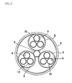
- FIG. 3 is a plan view from line A-A in FIG. 2 .
- the polishing apparatus shown in FIG. 2 and FIG. 3 comprises: a circular lower polishing surface plate 1 supported horizontally; a circular upper polishing surface plate 2 facing the lower polishing surface plate 1 from above; a sun gear 3 positioned at the inside of the circular lower polishing surface plate 1; and a ring-like internally-toothed gear 4 positioned at the outside of the lower polishing surface plate 1.
- reference numeral 5 denotes a cylinder
- reference numeral 6 denotes a joint
- reference numeral 7 denotes a tank for polishing liquid
- reference numeral 8 denotes carriers
- reference numeral 9 denotes holes for being set therein with wafer substrates 10.
- Facing surfaces of the lower polishing surface plate 1 and the upper polishing surface plate 2 are, as shown in FIG. 4 (a) to FIG. 4(c) , attached thereto pads (abrasive clothes) 15 and 25 each obtained by impregnating urethane resin into nonwoven fabric cloth, or pads (abrasive clothes) 15 and 25 comprised of urethane foams etc.
- polishing condition is set such that both surfaces of each wafer substrates 10 are evenly polished and the plurality of wafer substrates 10 are evenly polished.
- FIG. 4(a) to FIG. 4(c) are schematic cross-sectional views illustrating polishing statuses.
- the polishing pressures from the abrasive clothes 15 and 25 are allowed to be distributed toward adjacent wafer substrates 10 arranged close to each other as denoted by symbol B in FIG. 4 (c) . Consequently, disadvantages in the conventional technique are suppressed that the productivity may be deteriorated due to decreasing of the polishing rate and that the control of the thickness of carriers may be required, etc, while on the other hand, edge-roll-off of the wafer substrates 10 may be prevented from occurring at the outer edge portions thereof.
- the polishing method of the present embodiment by making smaller the distance between the wafer substrates 10 (distance between the holes 9), the deformation amount of the abrasive clothes 15 and 25 are allowed to be decreased in the vicinity of the position where adjacent wafer substrates 10 are close to each other. Consequently, the present embodiment allows the pressure concentration at the outer edge portions of the wafer substrates 10 to be alleviated in the vicinity of the outer edge portions of the wafer substrates 10. As a result, the occurrence of edge-roll-off of the wafer substrates 10 may be reduced at the outer edge portions thereof.
- the abrasive clothes 15 and 25 on the surfaces of the polishing surface plates having flexibility are deformed to outstand toward the carrier 8 from the height (the position in the thickness direction) at the planar position of the wafer substrate 10. Consequently, the pressures from the abrasive clothes 15 and 25 may be concentrated in the vicinity of the edge portion of the wafer substrate 10 along the entire length of the outer edge portion of the wafer substrate 10, thereby to possibly cause the occurrence of the edge-roll-off of the wafer substrate 10.
- the polishing method of the present embodiment through decreasing the distances among the wafer substrates 10 to be subjected to the double side polishing and causing the wafer substrates 10 to be close to one another, it is enabled to approach the status where the wafer substrates 10 positioned in three holes 9 within one carrier 8 are polished as if they are of one wafer substrate 10.
- any configuration of a part of the polishing apparatus may also be applicable so long as the arrangement of the holes 9 or the wafer substrates 10 within each carrier 8 complies with the above constitution.
- the polishing amount for the back surface of a silicon epitaxial wafer substrate is equal to or more than the polishing amount for the front surface.
- the polishing amount for the front surface of a wafer substrate is within the range of 0.01 to 0.1 ⁇ m, and the polishing amount for the back surface is within the range of 0.1 to 1.0 ⁇ m.
- the front surface of the wafer substrate is subjected to a mirror polishing.
- the polishing amount in the mirror polishing is, for example, 0.01 to 0.2 ⁇ m.
- the flatness of the wafer substrate is ensured by the first polishing step D to be performed before the epitaxial growth step F, and epitaxial defects may be reduced because polishing damages scarcely occurs due to the polishing not using abrasive grains.
- the double side concurrently polishing step G1 to be performed after the epitaxial growth step F the haze level of the surface of a wafer is improved.
- the double side concurrently polishing step G1 after the epitaxial growth may remove hitting flaws caused by susceptors in the epitaxial reactor furnace, which may occur on the back surface of the wafer, and also remove the depositions onto the back surface, thereby suppressing the degradation of flatness and/or the occurrence of particles due to such flaws and depositions.
- the double side concurrently polishing step G1 after the epitaxial growth allows the polishing amount of the wafer surfaces to be small as much as possible to the extent of removing oxidized layers on the surfaces, thereby maintaining the thickness of the epitaxial layers on the surfaces to be even.
- FIG. 5 depicts four silicon wafers produced by the production method according to the present embodiment as illustrated in FIG. 1 , wherein an average of six epitaxial defects per one silicon wafer is observed.
- the lower of FIG. 5 depicts four silicon wafers as comparative examples by using slurry containing abrasive grains in the first polishing step D as illustrated in FIG. 1 , wherein an average of 220 epitaxial defects per one silicon wafer is observed.
- the double side concurrently polishing step G1 is provided after the epitaxial growth step F in the above embodiments, this double side concurrently polishing step G1 may be omitted in the present invention. More specifically, it is enough to polish at least the front surface of a silicon single crystal substrate using slurry not containing abrasive grains in the first polishing step D and thereafter to perform epitaxial growth on that surface, and the subsequent double side concurrently polishing step G1 may thus be omitted. This allows for further improving the productivity.
Landscapes
- Chemical & Material Sciences (AREA)
- Engineering & Computer Science (AREA)
- Crystallography & Structural Chemistry (AREA)
- Materials Engineering (AREA)
- Metallurgy (AREA)
- Organic Chemistry (AREA)
- Chemical Kinetics & Catalysis (AREA)
- General Chemical & Material Sciences (AREA)
- Mechanical Engineering (AREA)
- Mechanical Treatment Of Semiconductor (AREA)
- Finish Polishing, Edge Sharpening, And Grinding By Specific Grinding Devices (AREA)
- Chemical Vapour Deposition (AREA)
Abstract
Description
- The present invention relates to a method for producing a silicon epitaxial wafer.
- A production method is known which grows a vapor phase epitaxial layer on the surface of a silicon single crystal wafer and then subjects the surface of the epitaxial layer to mirror polishing process (Patent Document 1). According to this production method, crown defects having occurred by the epitaxial growth are allowed to be removed and the flatness of the surface may be achieved.
-
- Patent Document 1: Examined Patent Publication No.
H8-17163 (1996 - However, the above prior art production method may not solve the problem that the productivity is significantly deteriorated because mirror polishing steps are employed before and after the epitaxial growth step.
- Problems to be solved by the present invention include providing a method for producing a silicon epitaxial wafer, in which the high productivity is obtained and epitaxial defects are also allowed to be decreased.
- The present invention solves the above problems by providing a first double side polishing step at which, before a growth step at which an epitaxial layer is grown on a silicon single crystal substrate, at least a front surface of the silicon single crystal substrate is polished using slurry free from abrasive grains, while providing a second polishing step at which at least the front surface of the silicon single crystal substrate is subjected to finish polishing after the growth step.
- According to the present invention, the productivity is allowed to be increased by polishing without using abrasive grains in the first double side polishing step. Moreover, epitaxial defects are allowed to be decreased because damages due to abrasive grains may be decreased.
-
- [
FIG. 1] FIG. 1 is a process chart illustrating a method for producing a silicon epitaxial wafer, to which an embodiment of the present invention is applied. - [
FIG. 2] FIG. 2 is a front elevational view illustrating one example of a polishing apparatus which is applied to the double side concurrently polishing step G1 inFIG. 1 . - [
FIG. 3] FIG. 3 is a plan view from line A-A inFIG. 2 . - [
FIG. 4] FIG. 4(a) to FIG. 4(c) are schematic cross-sectional views illustrating polishing statuses by the polishing apparatus inFIG. 2 . - [
FIG. 5] FIG. 5 depicts views illustrating epitaxial defects to be improved by the method inFIG. 1 - Hereinafter, embodiments of the present invention will be described with reference to the drawings.
-
FIG. 1 is a process chart illustrating a method for producing a silicon epitaxial wafer, to which an embodiment of the present invention is applied. - Describing at first one example of a pre-process for slicing step A, using Czochralski pulling up method, a p-type silicon single crystal ingot is produced which has the main axis orientation of <100> and the diameter of 305 mm, and this ingot is peripherally ground into the diameter of 300 mm and then subj ected to notch forming thereafter being cut into a plurality of blocks with electrical resistance of 5 to 10 mΩcm.
- Note that, as the main axis orientation of the silicon single crystal, other orientations, such as <110>, may be applicable alternatively to <100>. Also note that, as the diameter of the wafer, other diameters, such as 200 mm and 450 mm may be applicable alternatively to 300 mm.
- In the slicing step A, each of the above blocks is sliced using a wire saw to provide wafer-like substrates with a certain thickness.
- Sliced wafer substrates are subjected to double side grinding in lapping step B thereby to ensure a certain degree of flatness. In the lapping step B, the wafer substrates are interposed between upper and lower grinding surface plates of a double side grinding machine, and both surfaces, i.e. the front surface and the back surface of each wafer substrate are ground while supplying slurry containing abrasive grains.
- Wafer substrates having been flattened to a certain degree in the lapping step B are put into etching step C, and grinding damages generated on the surfaces are removed therefrom. Note that wafer substrates may be sent to a chamfering step after the lapping step B, and the shapes of outer faces thereof may be adjusted using grinding stone.
- In the producing method according to the present embodiment, first polishing step D is provided which polishes, before epitaxial growth step F, at least front surfaces of the wafer substrates having been completed the etching step C, only by an abrasive cloth and using slurry not containing abrasive grains.
- In this first polishing step D, only the front surface of each wafer substrate may be polished, or otherwise both the front surface and the back surface of each wafer substrate may be concurrently polished. In the case of concurrently polishing both surfaces, the wafer substrate is interposed between upper and lower polishing surface plates of a double side polishing apparatus, to which hard polishing pads are attached, and both surfaces of the wafer substrate are polished at the same time under the condition of no abrasive grains.
- The polishing amount in this first polishing step D is within the range of 5 to 30 µm, for example. This first polishing step D improves the flatness of wafer substrates and suppresses polishing damages due to abrasive grains from occurring because the polishing is performed without abrasive grains, and defects to be subsequently formed in the epitaxial layer would be reduced.
- Note that, after the etching step C and before the first polishing step D, polishing with abrasive grains may be performed to polish the surfaces of the wafer substrates using slurry containing abrasive grains, however, in this case, in order to remove polishing damages due to abrasive grains, it is preferred that the polishing amount in the first polishing step D is set to be 100 nm or more.
- After completing the first polishing step D, the wafer substrates are cleaned up to remove polishing residue (cleaning step E) thereafter being sent to the epitaxial growth step F.
- In the epitaxial growth step F, before supplying reactive gases into an epitaxial reactor furnace in which wafer substrates are set, halogenated gas may be supplied into the reactor furnace to remove oxidized films having formed on the surfaces of the wafer substrates. Alternatively to the method of etching by supplying halogenated gas into the epitaxial reactor furnace, the cleaning step E may be provided therein with a wet etching step where etching liquid for the oxidized films is dropped onto the wafer substrates.
- In the epitaxial growth step F, the wafer substrates are set on susceptors in the epitaxial reactor furnace and the reactive gases are supplied thereby to form epitaxial layers on the surfaces of the wafer substrates.
- Wafer substrates having formed thereon with epitaxial layers are sent to second polishing step G to be subjected to finish polishing. Although the second polishing step G is enough to be a step at which at least the front surface of each wafer substrate is subjected to the finish polishing, the second polishing step G according to the present embodiment involves double side concurrently polishing step G1 and subsequent single side mirror polishing step G2. Hereinafter, the double side concurrently polishing step G1 and the single side mirror polishing step G2 will be described as one example of the second polishing step G, but the present invention is not intended to be limited to this.
- In the double side concurrently polishing step G1, a double side polishing apparatus and a polishing method as shown in
FIG. 2 to FIGs. 4 (a) to 4 (c) may be employed. Hereinafter, one example of such polishing apparatus used in the double side concurrently polishing step G1 will be described.FIG. 2 is a front elevational view illustrating one example of the polishing apparatus, andFIG. 3 is a plan view from line A-A inFIG. 2 . - The polishing apparatus shown in
FIG. 2 andFIG. 3 comprises: a circular lowerpolishing surface plate 1 supported horizontally; a circular upperpolishing surface plate 2 facing the lowerpolishing surface plate 1 from above; asun gear 3 positioned at the inside of the circular lowerpolishing surface plate 1; and a ring-like internally-toothed gear 4 positioned at the outside of the lowerpolishing surface plate 1. In addition,reference numeral 5 denotes a cylinder, reference numeral 6 denotes a joint, reference numeral 7 denotes a tank for polishing liquid,reference numeral 8 denotes carriers, andreference numeral 9 denotes holes for being set therein withwafer substrates 10. - Facing surfaces of the lower
polishing surface plate 1 and the upperpolishing surface plate 2 are, as shown inFIG. 4 (a) to FIG. 4(c) , attached thereto pads (abrasive clothes) 15 and 25 each obtained by impregnating urethane resin into nonwoven fabric cloth, or pads (abrasive clothes) 15 and 25 comprised of urethane foams etc. - When performing the polishing of
wafer substrates 10, in the status where the upperpolishing surface plate 2 is lifted up, a plurality ofcarriers 8 are set on the lowerpolishing surface plate 1 and thewafer substrates 10 are set intoholes 9 of eachcarrier 8. The upperpolishing surface plate 2 is then caused to move down to apply a predetermined pressing force to eachwafer substrate 10. In this status, while polishing liquid is supplied between the lowerpolishing surface plate 1 and the upperpolishing surface plate 2, the lowerpolishing surface plate 1, the upperpolishing surface plate 2, thesun gear 3, and the internally-toothed gear 4 are caused to rotate in predetermined directions with predetermined speeds. - This allows a sun-and-planet motion to run where the plurality of
carriers 8 revolve around thesun gear 3 while each rotating between the lowerpolishing surface plate 1 and the upperpolishing surface plate 2. Thewafer substrates 10 held by eachcarrier 8 are contacted and rubbed with theabrasive clothes wafer substrates 10 are evenly polished and the plurality ofwafer substrates 10 are evenly polished. -
FIG. 4(a) to FIG. 4(c) are schematic cross-sectional views illustrating polishing statuses. - In the conventional polishing technique which involves a polishing
step using carriers 8 thinner thanwafer substrates 10, pressures from theabrasive clothes wafer substrates 10, one of which is denoted by symbol A inFIG. 4(a) , thereby causing edge-roll-off to occur in eachwafer substrate 10 as a result. In addition, according to the polishing technique described in Jpn. Unexamined Patent Publication No. 2002-254299, as shown inFIG. 4(b) , a method is employed in which the pressures to be concentrated at outer edges A are distributed toward the vicinity ofwafer substrates 10 and thecarriers 8 by enlarging the thickness dimensions of thecarriers 8. - In contrast, according to the polishing method of the present embodiment, by closely arranging the
holes 9 in the planar arrangement within eachcarrier 8 to concentrate the locations of thewafer substrates 10 toward the center of eachcarrier 8, as shown inFIG. 4(c) , the polishing pressures from theabrasive clothes adjacent wafer substrates 10 arranged close to each other as denoted by symbol B inFIG. 4 (c) . Consequently, disadvantages in the conventional technique are suppressed that the productivity may be deteriorated due to decreasing of the polishing rate and that the control of the thickness of carriers may be required, etc, while on the other hand, edge-roll-off of thewafer substrates 10 may be prevented from occurring at the outer edge portions thereof. - This is considered as being due to that the distances among the
wafer substrates 10 are made smaller in the status of eliminating the influence from the deformation ofcarriers 8 by thewafer substrates 10 during polishing, etc. Consequently, the concentration of polishing pressures from theabrasive clothes surface plates wafer substrates 10 is suppressed from occurring in the vicinity of the position whereadjacent wafer substrates 10 come to be most close to each other. - During operation of the polishing, at the position between a
wafer substrate 10 and anotherwafer substrate 10, due to the difference in thickness between thewafer substrates 10 and thecarrier 8, a status is provided where theabrasive clothes carrier 8 from the height (the position in the thickness direction) at the planar position of eachwafer substrate 10. For this reason, the pressures from theabrasive clothes wafer substrates 10 thereby to increase the polishing amount at the edge portions of thewafer substrates 10. - According to the polishing method of the present embodiment, however, as shown in
FIG. 4(c) , by making smaller the distance between the wafer substrates 10 (distance between the holes 9), the deformation amount of theabrasive clothes adjacent wafer substrates 10 are close to each other. Consequently, the present embodiment allows the pressure concentration at the outer edge portions of thewafer substrates 10 to be alleviated in the vicinity of the outer edge portions of thewafer substrates 10. As a result, the occurrence of edge-roll-off of thewafer substrates 10 may be reduced at the outer edge portions thereof. - This enables to easily and appropriately perform the polishing to a predetermined amount and to easily perceive the ending point of polishing, and to avoid the polishing pressure degradation to the
wafer substrates 10 due to the decreasing of the pressure from the polishing surface plates to thecarriers 8 even if during the latter half of the polishing step thereby to prevent the operation time efficiency/polishing efficiency from deteriorating, and also prevents thecarriers 8 from being polished thereby to obtain long life-time thereof, and additionally avoids the flatness deterioration and the like by preventing the occurrence of edge-roll-off thereby enabling to produce thewafer substrates 10 having high flatness. - Moreover, during the polishing operation, in the vicinity of the border, as the outer edge portion of each
wafer substrate 10, between thewafer substrate 10 and thecarrier 8, due to the difference in thickness between thewafer substrate 10 being polished and thecarrier 8, theabrasive clothes carrier 8 from the height (the position in the thickness direction) at the planar position of thewafer substrate 10. Consequently, the pressures from theabrasive clothes wafer substrate 10 along the entire length of the outer edge portion of thewafer substrate 10, thereby to possibly cause the occurrence of the edge-roll-off of thewafer substrate 10. - According to the polishing method of the present embodiment, however, through decreasing the distances among the
wafer substrates 10 to be subjected to the double side polishing and causing thewafer substrates 10 to be close to one another, it is enabled to approach the status where thewafer substrates 10 positioned in threeholes 9 within onecarrier 8 are polished as if they are of onewafer substrate 10. This allows to limit the length where the stress concentration occurs relative to the entire outer edge length of onewafer substrate 10, that is, to reduce the area where the polishing condition within the outer edge portion of thewafer substrate 10 becomes to be significant because the pressures from theabrasive clothes surface plates wafer substrate 10 due to the difference in thickness between thewafer substrate 10 and thecarrier 8. Consequently, the polishing pressure concentration is allowed to be alleviated for the entire length of the edge portion of onewafer substrate 10 at the time of completing the polishing, and the occurrence of the edge-roll-off along the outer edge portion of eachwafer substrate 10 is also allowed to be reduced. - Although the depicted example employs the configuration involving three
carriers 8, other number thereof may also be applicable, and other than this, any configuration of a part of the polishing apparatus may also be applicable so long as the arrangement of theholes 9 or thewafer substrates 10 within eachcarrier 8 complies with the above constitution. - Referring again to
FIG. 1 , in the double side concurrently polishing step G1 of the second polishing step G, it is preferred that the polishing amount for the back surface of a silicon epitaxial wafer substrate is equal to or more than the polishing amount for the front surface. For example, it is preferred that the polishing amount for the front surface of a wafer substrate is within the range of 0.01 to 0.1 µm, and the polishing amount for the back surface is within the range of 0.1 to 1.0 µm. - In the subsequent single side mirror polishing step G2, the front surface of the wafer substrate is subjected to a mirror polishing. The polishing amount in the mirror polishing is, for example, 0.01 to 0.2 µm.
- As described above, according to the method for producing a silicon epitaxial wafer in the present embodiment, the flatness of the wafer substrate is ensured by the first polishing step D to be performed before the epitaxial growth step F, and epitaxial defects may be reduced because polishing damages scarcely occurs due to the polishing not using abrasive grains.
- On the other hand, according to the double side concurrently polishing step G1 to be performed after the epitaxial growth step F, the haze level of the surface of a wafer is improved. At the same time, the double side concurrently polishing step G1 after the epitaxial growth may remove hitting flaws caused by susceptors in the epitaxial reactor furnace, which may occur on the back surface of the wafer, and also remove the depositions onto the back surface, thereby suppressing the degradation of flatness and/or the occurrence of particles due to such flaws and depositions.
- Moreover, the double side concurrently polishing step G1 after the epitaxial growth allows the polishing amount of the wafer surfaces to be small as much as possible to the extent of removing oxidized layers on the surfaces, thereby maintaining the thickness of the epitaxial layers on the surfaces to be even.
- The upper of
FIG. 5 depicts four silicon wafers produced by the production method according to the present embodiment as illustrated inFIG. 1 , wherein an average of six epitaxial defects per one silicon wafer is observed. In contrast, the lower ofFIG. 5 depicts four silicon wafers as comparative examples by using slurry containing abrasive grains in the first polishing step D as illustrated inFIG. 1 , wherein an average of 220 epitaxial defects per one silicon wafer is observed. - It is to be noted that the embodiments as explained above are described to facilitate understanding of the present invention and are not described to limit the present invention. Therefore, it is intended that the elements disclosed in the above embodiments include all design changes and equivalents to fall within the technical scope of the present invention.
- For example, although the double side concurrently polishing step G1 is provided after the epitaxial growth step F in the above embodiments, this double side concurrently polishing step G1 may be omitted in the present invention. More specifically, it is enough to polish at least the front surface of a silicon single crystal substrate using slurry not containing abrasive grains in the first polishing step D and thereafter to perform epitaxial growth on that surface, and the subsequent double side concurrently polishing step G1 may thus be omitted. This allows for further improving the productivity.
-
- 1
- lower polishing surface plate
- 2
- upper polishing surface plate
- 3
- sun gear
- 4
- internally-toothed gear
- 8
- carrier
- 9
- hole
- 10
- silicon wafer substrate
Claims (9)
- A method for producing a silicon epitaxial wafer, comprising:a growth step at which an epitaxial layer is grown on a silicon single crystal substrate;a first polishing step at which, before the growth step, at least a front surface of the silicon single crystal substrate is polished without using abrasive grains; anda second polishing step at which at least the front surface of the silicon single crystal substrate is subjected to finish polishing after the growth step.
- The method for producing a silicon epitaxial wafer as set forth in claim 1, further comprising
a polishing step at which a polishing is performed by using abrasive grains before the first polishing step. - The method for producing a silicon epitaxial wafer as set forth in claim 2, wherein
a polishing amount in the first polishing step is 100 nm or more. - The method for producing a silicon epitaxial wafer as set forth in any one of claims 1 to 3, wherein
the second polishing step has: a first step at which both main surfaces of the silicon single crystal substrate are polished; and a second step at which the front surface of the silicon single crystal substrate is subjected to mirror polishing. - The method for producing a silicon epitaxial wafer as set forth in claim 4, wherein
a polishing amount for a back surface of the silicon single crystal substrate in the second step is equal to or more than a polishing amount for the front surface. - The method for producing a silicon epitaxial wafer as set forth in claim 5, wherein
the polishing amount for the back surface is 0.1 to 1.0 µm. - The method for producing a silicon epitaxial wafer as set forth in any one of claims 1 to 3, wherein
only the front surface of the silicon single crystal substrate is subjected to mirror polishing in the second polishing step. - The method for producing a silicon epitaxial wafer as set forth in any one of claims 1 to 7, wherein
the growth step includes etching step at which, before growing the epitaxial layer, oxidized films having formed on surfaces of the silicon single crystal substrate are removed by halogenated gas. - The method for producing a silicon epitaxial wafer as set forth in any one of claims 1 to 7, further comprising
an etching step at which surfaces of the silicon single crystal substrate are subjected to wet etching process between the first polishing step and the growth step.
Applications Claiming Priority (2)
| Application Number | Priority Date | Filing Date | Title |
|---|---|---|---|
| JP2009096800 | 2009-04-13 | ||
| PCT/JP2010/056517 WO2010119833A1 (en) | 2009-04-13 | 2010-04-12 | Method for producing silicon epitaxial wafer |
Publications (3)
| Publication Number | Publication Date |
|---|---|
| EP2421028A1 true EP2421028A1 (en) | 2012-02-22 |
| EP2421028A4 EP2421028A4 (en) | 2013-01-02 |
| EP2421028B1 EP2421028B1 (en) | 2015-11-04 |
Family
ID=42982495
Family Applications (1)
| Application Number | Title | Priority Date | Filing Date |
|---|---|---|---|
| EP10764417.1A Active EP2421028B1 (en) | 2009-04-13 | 2010-04-12 | Method for producing silicon epitaxial wafer |
Country Status (7)
| Country | Link |
|---|---|
| US (1) | US8673784B2 (en) |
| EP (1) | EP2421028B1 (en) |
| JP (1) | JP5287982B2 (en) |
| KR (1) | KR101322969B1 (en) |
| MY (1) | MY154627A (en) |
| TW (1) | TWI474389B (en) |
| WO (1) | WO2010119833A1 (en) |
Cited By (1)
| Publication number | Priority date | Publication date | Assignee | Title |
|---|---|---|---|---|
| US10813002B2 (en) | 2013-07-18 | 2020-10-20 | Convida Wireless, Llc | Capillary device charging |
Families Citing this family (1)
| Publication number | Priority date | Publication date | Assignee | Title |
|---|---|---|---|---|
| KR102660335B1 (en) | 2018-05-02 | 2024-04-23 | 고쿠리츠다이가쿠호진 도호쿠다이가쿠 | Method for producing heated ozonated water, heated ozonated water and semiconductor wafer cleaning liquid |
Family Cites Families (22)
| Publication number | Priority date | Publication date | Assignee | Title |
|---|---|---|---|---|
| US3436259A (en) | 1966-05-12 | 1969-04-01 | Ibm | Method for plating and polishing a silicon planar surface |
| JPS54110783A (en) * | 1978-02-20 | 1979-08-30 | Hitachi Ltd | Semiconductor substrate and its manufacture |
| JPH0817163B2 (en) | 1990-04-12 | 1996-02-21 | 株式会社東芝 | Epitaxial wafer manufacturing method |
| JPH04122023A (en) | 1990-09-13 | 1992-04-22 | Hitachi Ltd | Method for manufacturing semiconductor wafers and methods for manufacturing semiconductor integrated circuit devices |
| JPH0817163A (en) | 1994-06-29 | 1996-01-19 | Sony Corp | Disk cartridge |
| JP3317330B2 (en) | 1995-12-27 | 2002-08-26 | 信越半導体株式会社 | Manufacturing method of semiconductor mirror surface wafer |
| DE19704546A1 (en) | 1997-02-06 | 1998-08-13 | Wacker Siltronic Halbleitermat | Process for producing a semiconductor wafer coated on one side and provided with a finish |
| DE19938340C1 (en) * | 1999-08-13 | 2001-02-15 | Wacker Siltronic Halbleitermat | Production of semiconductor wafer comprises simultaneously polishing the front and rear sides of wafer between rotating polishing plates using an alkaline polishing sol and then an alcohol, cleaning, drying and applying an epitaxial layer |
| JP3932756B2 (en) | 2000-02-09 | 2007-06-20 | 信越半導体株式会社 | Manufacturing method of silicon epitaxial wafer |
| US20020127766A1 (en) * | 2000-12-27 | 2002-09-12 | Memc Electronic Materials, Inc. | Semiconductor wafer manufacturing process |
| JP3991598B2 (en) | 2001-02-26 | 2007-10-17 | 株式会社Sumco | Wafer polishing method |
| US6863595B1 (en) * | 2001-12-19 | 2005-03-08 | Cypress Semiconductor Corp. | Methods for polishing a semiconductor topography |
| US6849548B2 (en) * | 2002-04-05 | 2005-02-01 | Seh America, Inc. | Method of reducing particulate contamination during polishing of a wafer |
| JP4511801B2 (en) | 2003-03-14 | 2010-07-28 | 株式会社リコー | Group III nitride crystal polishing method, group III nitride crystal and semiconductor device |
| JP4273943B2 (en) * | 2003-12-01 | 2009-06-03 | 株式会社Sumco | Silicon wafer manufacturing method |
| JP4240403B2 (en) * | 2003-12-11 | 2009-03-18 | 株式会社Sumco | Epitaxial wafer manufacturing method |
| EP1605498A1 (en) * | 2004-06-11 | 2005-12-14 | S.O.I. Tec Silicon on Insulator Technologies S.A. | A method of manufacturing a semiconductor wafer |
| JP2006120939A (en) * | 2004-10-22 | 2006-05-11 | Shin Etsu Handotai Co Ltd | Method for manufacturing silicon epitaxial wafer |
| JP4122023B2 (en) | 2005-11-08 | 2008-07-23 | 大日本印刷株式会社 | Printed matter |
| JP5029234B2 (en) | 2006-09-06 | 2012-09-19 | 株式会社Sumco | Epitaxial wafer manufacturing method |
| JPWO2009081720A1 (en) | 2007-12-21 | 2011-05-06 | 株式会社Sumco | Epitaxial silicon wafer manufacturing method |
| TW201000693A (en) * | 2008-06-05 | 2010-01-01 | Sumco Corp | Epitaxial silicon wafer and method for producing the same |
-
2010
- 2010-04-12 KR KR1020117026721A patent/KR101322969B1/en active Active
- 2010-04-12 MY MYPI2011004880A patent/MY154627A/en unknown
- 2010-04-12 US US13/264,057 patent/US8673784B2/en active Active
- 2010-04-12 EP EP10764417.1A patent/EP2421028B1/en active Active
- 2010-04-12 WO PCT/JP2010/056517 patent/WO2010119833A1/en not_active Ceased
- 2010-04-12 JP JP2011509281A patent/JP5287982B2/en active Active
- 2010-04-13 TW TW99111428A patent/TWI474389B/en active
Cited By (2)
| Publication number | Priority date | Publication date | Assignee | Title |
|---|---|---|---|---|
| US10813002B2 (en) | 2013-07-18 | 2020-10-20 | Convida Wireless, Llc | Capillary device charging |
| US11736968B2 (en) | 2013-07-18 | 2023-08-22 | Interdigital Patent Holdings, Inc. | Capillary device charging |
Also Published As
| Publication number | Publication date |
|---|---|
| US20120034850A1 (en) | 2012-02-09 |
| WO2010119833A1 (en) | 2010-10-21 |
| KR101322969B1 (en) | 2013-12-19 |
| JPWO2010119833A1 (en) | 2012-10-22 |
| KR20120000578A (en) | 2012-01-02 |
| US8673784B2 (en) | 2014-03-18 |
| EP2421028A4 (en) | 2013-01-02 |
| EP2421028B1 (en) | 2015-11-04 |
| JP5287982B2 (en) | 2013-09-11 |
| MY154627A (en) | 2015-07-15 |
| TWI474389B (en) | 2015-02-21 |
| TW201110216A (en) | 2011-03-16 |
Similar Documents
| Publication | Publication Date | Title |
|---|---|---|
| US10269554B2 (en) | Method for manufacturing SiC epitaxial wafer and SiC epitaxial wafer | |
| US9293318B2 (en) | Semiconductor wafer manufacturing method | |
| JP5177290B2 (en) | Fixed abrasive processing apparatus, fixed abrasive processing method, and semiconductor wafer manufacturing method | |
| KR101605384B1 (en) | Double-head grinding apparatus and wafer manufacturing method | |
| JPH0997775A (en) | Method for manufacturing semiconductor mirror surface wafer | |
| JP5600867B2 (en) | Manufacturing method of semiconductor wafer | |
| KR20090029270A (en) | Carrier for double side polishing apparatus, double side polishing apparatus and double side polishing method using same | |
| US7601644B2 (en) | Method for manufacturing silicon wafers | |
| WO2015037188A1 (en) | Production method for mirror polished wafers | |
| WO2014171059A1 (en) | Method for polishing silicon wafer and method for producing epitaxial wafer | |
| JP2009302410A (en) | Method of manufacturing semiconductor wafer | |
| KR20110016822A (en) | Polishing Semiconductor Wafer Manufacturing Method | |
| US8999061B2 (en) | Method for producing silicon epitaxial wafer | |
| JP7168113B1 (en) | Wafer double-sided polishing method | |
| EP1699074B1 (en) | Manufacturing method of silicon wafer | |
| EP2421028B1 (en) | Method for producing silicon epitaxial wafer | |
| JP4492293B2 (en) | Manufacturing method of semiconductor substrate | |
| JP4103808B2 (en) | Wafer grinding method and wafer | |
| JP2011091143A (en) | Method of manufacturing silicon epitaxial wafer | |
| JP2005209862A (en) | Method for manufacturing semiconductor epitaxial wafer | |
| KR100864347B1 (en) | Silicon Wafer Manufacturing Method |
Legal Events
| Date | Code | Title | Description |
|---|---|---|---|
| PUAI | Public reference made under article 153(3) epc to a published international application that has entered the european phase |
Free format text: ORIGINAL CODE: 0009012 |
|
| 17P | Request for examination filed |
Effective date: 20111108 |
|
| AK | Designated contracting states |
Kind code of ref document: A1 Designated state(s): AT BE BG CH CY CZ DE DK EE ES FI FR GB GR HR HU IE IS IT LI LT LU LV MC MK MT NL NO PL PT RO SE SI SK SM TR |
|
| DAX | Request for extension of the european patent (deleted) | ||
| REG | Reference to a national code |
Ref country code: DE Ref legal event code: R079 Ref document number: 602010028816 Country of ref document: DE Free format text: PREVIOUS MAIN CLASS: H01L0021304000 Ipc: B24B0037040000 |
|
| A4 | Supplementary search report drawn up and despatched |
Effective date: 20121129 |
|
| RIC1 | Information provided on ipc code assigned before grant |
Ipc: H01L 21/02 20060101ALI20121123BHEP Ipc: C30B 29/06 20060101ALI20121123BHEP Ipc: C30B 25/18 20060101ALI20121123BHEP Ipc: H01L 21/306 20060101ALI20121123BHEP Ipc: B24B 37/04 20120101AFI20121123BHEP |
|
| GRAJ | Information related to disapproval of communication of intention to grant by the applicant or resumption of examination proceedings by the epo deleted |
Free format text: ORIGINAL CODE: EPIDOSDIGR1 |
|
| GRAP | Despatch of communication of intention to grant a patent |
Free format text: ORIGINAL CODE: EPIDOSNIGR1 |
|
| INTG | Intention to grant announced |
Effective date: 20150522 |
|
| GRAS | Grant fee paid |
Free format text: ORIGINAL CODE: EPIDOSNIGR3 |
|
| GRAA | (expected) grant |
Free format text: ORIGINAL CODE: 0009210 |
|
| AK | Designated contracting states |
Kind code of ref document: B1 Designated state(s): AT BE BG CH CY CZ DE DK EE ES FI FR GB GR HR HU IE IS IT LI LT LU LV MC MK MT NL NO PL PT RO SE SI SK SM TR |
|
| REG | Reference to a national code |
Ref country code: GB Ref legal event code: FG4D |
|
| REG | Reference to a national code |
Ref country code: CH Ref legal event code: EP |
|
| REG | Reference to a national code |
Ref country code: AT Ref legal event code: REF Ref document number: 758861 Country of ref document: AT Kind code of ref document: T Effective date: 20151115 |
|
| REG | Reference to a national code |
Ref country code: IE Ref legal event code: FG4D |
|
| REG | Reference to a national code |
Ref country code: DE Ref legal event code: R096 Ref document number: 602010028816 Country of ref document: DE |
|
| REG | Reference to a national code |
Ref country code: NL Ref legal event code: MP Effective date: 20151104 |
|
| REG | Reference to a national code |
Ref country code: LT Ref legal event code: MG4D |
|
| REG | Reference to a national code |
Ref country code: AT Ref legal event code: MK05 Ref document number: 758861 Country of ref document: AT Kind code of ref document: T Effective date: 20151104 |
|
| PG25 | Lapsed in a contracting state [announced via postgrant information from national office to epo] |
Ref country code: HR Free format text: LAPSE BECAUSE OF FAILURE TO SUBMIT A TRANSLATION OF THE DESCRIPTION OR TO PAY THE FEE WITHIN THE PRESCRIBED TIME-LIMIT Effective date: 20151104 Ref country code: NO Free format text: LAPSE BECAUSE OF FAILURE TO SUBMIT A TRANSLATION OF THE DESCRIPTION OR TO PAY THE FEE WITHIN THE PRESCRIBED TIME-LIMIT Effective date: 20160204 Ref country code: IT Free format text: LAPSE BECAUSE OF FAILURE TO SUBMIT A TRANSLATION OF THE DESCRIPTION OR TO PAY THE FEE WITHIN THE PRESCRIBED TIME-LIMIT Effective date: 20151104 Ref country code: ES Free format text: LAPSE BECAUSE OF FAILURE TO SUBMIT A TRANSLATION OF THE DESCRIPTION OR TO PAY THE FEE WITHIN THE PRESCRIBED TIME-LIMIT Effective date: 20151104 Ref country code: IS Free format text: LAPSE BECAUSE OF FAILURE TO SUBMIT A TRANSLATION OF THE DESCRIPTION OR TO PAY THE FEE WITHIN THE PRESCRIBED TIME-LIMIT Effective date: 20160304 Ref country code: NL Free format text: LAPSE BECAUSE OF FAILURE TO SUBMIT A TRANSLATION OF THE DESCRIPTION OR TO PAY THE FEE WITHIN THE PRESCRIBED TIME-LIMIT Effective date: 20151104 Ref country code: LT Free format text: LAPSE BECAUSE OF FAILURE TO SUBMIT A TRANSLATION OF THE DESCRIPTION OR TO PAY THE FEE WITHIN THE PRESCRIBED TIME-LIMIT Effective date: 20151104 |
|
| PG25 | Lapsed in a contracting state [announced via postgrant information from national office to epo] |
Ref country code: SE Free format text: LAPSE BECAUSE OF FAILURE TO SUBMIT A TRANSLATION OF THE DESCRIPTION OR TO PAY THE FEE WITHIN THE PRESCRIBED TIME-LIMIT Effective date: 20151104 Ref country code: PT Free format text: LAPSE BECAUSE OF FAILURE TO SUBMIT A TRANSLATION OF THE DESCRIPTION OR TO PAY THE FEE WITHIN THE PRESCRIBED TIME-LIMIT Effective date: 20160304 Ref country code: LV Free format text: LAPSE BECAUSE OF FAILURE TO SUBMIT A TRANSLATION OF THE DESCRIPTION OR TO PAY THE FEE WITHIN THE PRESCRIBED TIME-LIMIT Effective date: 20151104 Ref country code: PL Free format text: LAPSE BECAUSE OF FAILURE TO SUBMIT A TRANSLATION OF THE DESCRIPTION OR TO PAY THE FEE WITHIN THE PRESCRIBED TIME-LIMIT Effective date: 20151104 Ref country code: FI Free format text: LAPSE BECAUSE OF FAILURE TO SUBMIT A TRANSLATION OF THE DESCRIPTION OR TO PAY THE FEE WITHIN THE PRESCRIBED TIME-LIMIT Effective date: 20151104 Ref country code: GR Free format text: LAPSE BECAUSE OF FAILURE TO SUBMIT A TRANSLATION OF THE DESCRIPTION OR TO PAY THE FEE WITHIN THE PRESCRIBED TIME-LIMIT Effective date: 20160205 Ref country code: AT Free format text: LAPSE BECAUSE OF FAILURE TO SUBMIT A TRANSLATION OF THE DESCRIPTION OR TO PAY THE FEE WITHIN THE PRESCRIBED TIME-LIMIT Effective date: 20151104 |
|
| PG25 | Lapsed in a contracting state [announced via postgrant information from national office to epo] |
Ref country code: CZ Free format text: LAPSE BECAUSE OF FAILURE TO SUBMIT A TRANSLATION OF THE DESCRIPTION OR TO PAY THE FEE WITHIN THE PRESCRIBED TIME-LIMIT Effective date: 20151104 |
|
| REG | Reference to a national code |
Ref country code: DE Ref legal event code: R097 Ref document number: 602010028816 Country of ref document: DE |
|
| PG25 | Lapsed in a contracting state [announced via postgrant information from national office to epo] |
Ref country code: RO Free format text: LAPSE BECAUSE OF FAILURE TO SUBMIT A TRANSLATION OF THE DESCRIPTION OR TO PAY THE FEE WITHIN THE PRESCRIBED TIME-LIMIT Effective date: 20151104 Ref country code: DK Free format text: LAPSE BECAUSE OF FAILURE TO SUBMIT A TRANSLATION OF THE DESCRIPTION OR TO PAY THE FEE WITHIN THE PRESCRIBED TIME-LIMIT Effective date: 20151104 Ref country code: BE Free format text: LAPSE BECAUSE OF NON-PAYMENT OF DUE FEES Effective date: 20160430 Ref country code: SK Free format text: LAPSE BECAUSE OF FAILURE TO SUBMIT A TRANSLATION OF THE DESCRIPTION OR TO PAY THE FEE WITHIN THE PRESCRIBED TIME-LIMIT Effective date: 20151104 Ref country code: SM Free format text: LAPSE BECAUSE OF FAILURE TO SUBMIT A TRANSLATION OF THE DESCRIPTION OR TO PAY THE FEE WITHIN THE PRESCRIBED TIME-LIMIT Effective date: 20151104 Ref country code: EE Free format text: LAPSE BECAUSE OF FAILURE TO SUBMIT A TRANSLATION OF THE DESCRIPTION OR TO PAY THE FEE WITHIN THE PRESCRIBED TIME-LIMIT Effective date: 20151104 |
|
| PLBE | No opposition filed within time limit |
Free format text: ORIGINAL CODE: 0009261 |
|
| STAA | Information on the status of an ep patent application or granted ep patent |
Free format text: STATUS: NO OPPOSITION FILED WITHIN TIME LIMIT |
|
| 26N | No opposition filed |
Effective date: 20160805 |
|
| PG25 | Lapsed in a contracting state [announced via postgrant information from national office to epo] |
Ref country code: SI Free format text: LAPSE BECAUSE OF FAILURE TO SUBMIT A TRANSLATION OF THE DESCRIPTION OR TO PAY THE FEE WITHIN THE PRESCRIBED TIME-LIMIT Effective date: 20151104 |
|
| REG | Reference to a national code |
Ref country code: CH Ref legal event code: PL |
|
| GBPC | Gb: european patent ceased through non-payment of renewal fee |
Effective date: 20160412 |
|
| PG25 | Lapsed in a contracting state [announced via postgrant information from national office to epo] |
Ref country code: LU Free format text: LAPSE BECAUSE OF FAILURE TO SUBMIT A TRANSLATION OF THE DESCRIPTION OR TO PAY THE FEE WITHIN THE PRESCRIBED TIME-LIMIT Effective date: 20160412 Ref country code: BE Free format text: LAPSE BECAUSE OF FAILURE TO SUBMIT A TRANSLATION OF THE DESCRIPTION OR TO PAY THE FEE WITHIN THE PRESCRIBED TIME-LIMIT Effective date: 20151104 |
|
| REG | Reference to a national code |
Ref country code: IE Ref legal event code: MM4A |
|
| REG | Reference to a national code |
Ref country code: FR Ref legal event code: ST Effective date: 20161230 |
|
| PG25 | Lapsed in a contracting state [announced via postgrant information from national office to epo] |
Ref country code: FR Free format text: LAPSE BECAUSE OF NON-PAYMENT OF DUE FEES Effective date: 20160502 Ref country code: GB Free format text: LAPSE BECAUSE OF NON-PAYMENT OF DUE FEES Effective date: 20160412 Ref country code: LI Free format text: LAPSE BECAUSE OF NON-PAYMENT OF DUE FEES Effective date: 20160430 Ref country code: CH Free format text: LAPSE BECAUSE OF NON-PAYMENT OF DUE FEES Effective date: 20160430 |
|
| PG25 | Lapsed in a contracting state [announced via postgrant information from national office to epo] |
Ref country code: IE Free format text: LAPSE BECAUSE OF NON-PAYMENT OF DUE FEES Effective date: 20160412 |
|
| PG25 | Lapsed in a contracting state [announced via postgrant information from national office to epo] |
Ref country code: CY Free format text: LAPSE BECAUSE OF FAILURE TO SUBMIT A TRANSLATION OF THE DESCRIPTION OR TO PAY THE FEE WITHIN THE PRESCRIBED TIME-LIMIT Effective date: 20151104 Ref country code: HU Free format text: LAPSE BECAUSE OF FAILURE TO SUBMIT A TRANSLATION OF THE DESCRIPTION OR TO PAY THE FEE WITHIN THE PRESCRIBED TIME-LIMIT; INVALID AB INITIO Effective date: 20100412 |
|
| PG25 | Lapsed in a contracting state [announced via postgrant information from national office to epo] |
Ref country code: MK Free format text: LAPSE BECAUSE OF FAILURE TO SUBMIT A TRANSLATION OF THE DESCRIPTION OR TO PAY THE FEE WITHIN THE PRESCRIBED TIME-LIMIT Effective date: 20151104 Ref country code: MC Free format text: LAPSE BECAUSE OF FAILURE TO SUBMIT A TRANSLATION OF THE DESCRIPTION OR TO PAY THE FEE WITHIN THE PRESCRIBED TIME-LIMIT Effective date: 20151104 Ref country code: TR Free format text: LAPSE BECAUSE OF FAILURE TO SUBMIT A TRANSLATION OF THE DESCRIPTION OR TO PAY THE FEE WITHIN THE PRESCRIBED TIME-LIMIT Effective date: 20151104 Ref country code: MT Free format text: LAPSE BECAUSE OF NON-PAYMENT OF DUE FEES Effective date: 20160430 |
|
| PG25 | Lapsed in a contracting state [announced via postgrant information from national office to epo] |
Ref country code: BG Free format text: LAPSE BECAUSE OF FAILURE TO SUBMIT A TRANSLATION OF THE DESCRIPTION OR TO PAY THE FEE WITHIN THE PRESCRIBED TIME-LIMIT Effective date: 20151104 |
|
| PGFP | Annual fee paid to national office [announced via postgrant information from national office to epo] |
Ref country code: DE Payment date: 20250422 Year of fee payment: 16 |