EP2420990A1 - Display apparatus and power supplying method performed by display apparatus - Google Patents
Display apparatus and power supplying method performed by display apparatus Download PDFInfo
- Publication number
- EP2420990A1 EP2420990A1 EP11178192A EP11178192A EP2420990A1 EP 2420990 A1 EP2420990 A1 EP 2420990A1 EP 11178192 A EP11178192 A EP 11178192A EP 11178192 A EP11178192 A EP 11178192A EP 2420990 A1 EP2420990 A1 EP 2420990A1
- Authority
- EP
- European Patent Office
- Prior art keywords
- voltage
- power
- output
- panel
- input line
- Prior art date
- Legal status (The legal status is an assumption and is not a legal conclusion. Google has not performed a legal analysis and makes no representation as to the accuracy of the status listed.)
- Granted
Links
Images



Classifications
-
- G—PHYSICS
- G09—EDUCATION; CRYPTOGRAPHY; DISPLAY; ADVERTISING; SEALS
- G09G—ARRANGEMENTS OR CIRCUITS FOR CONTROL OF INDICATING DEVICES USING STATIC MEANS TO PRESENT VARIABLE INFORMATION
- G09G3/00—Control arrangements or circuits, of interest only in connection with visual indicators other than cathode-ray tubes
- G09G3/20—Control arrangements or circuits, of interest only in connection with visual indicators other than cathode-ray tubes for presentation of an assembly of a number of characters, e.g. a page, by composing the assembly by combination of individual elements arranged in a matrix no fixed position being assigned to or needed to be assigned to the individual characters or partial characters
-
- G—PHYSICS
- G09—EDUCATION; CRYPTOGRAPHY; DISPLAY; ADVERTISING; SEALS
- G09G—ARRANGEMENTS OR CIRCUITS FOR CONTROL OF INDICATING DEVICES USING STATIC MEANS TO PRESENT VARIABLE INFORMATION
- G09G3/00—Control arrangements or circuits, of interest only in connection with visual indicators other than cathode-ray tubes
- G09G3/20—Control arrangements or circuits, of interest only in connection with visual indicators other than cathode-ray tubes for presentation of an assembly of a number of characters, e.g. a page, by composing the assembly by combination of individual elements arranged in a matrix no fixed position being assigned to or needed to be assigned to the individual characters or partial characters
- G09G3/22—Control arrangements or circuits, of interest only in connection with visual indicators other than cathode-ray tubes for presentation of an assembly of a number of characters, e.g. a page, by composing the assembly by combination of individual elements arranged in a matrix no fixed position being assigned to or needed to be assigned to the individual characters or partial characters using controlled light sources
- G09G3/30—Control arrangements or circuits, of interest only in connection with visual indicators other than cathode-ray tubes for presentation of an assembly of a number of characters, e.g. a page, by composing the assembly by combination of individual elements arranged in a matrix no fixed position being assigned to or needed to be assigned to the individual characters or partial characters using controlled light sources using electroluminescent panels
- G09G3/32—Control arrangements or circuits, of interest only in connection with visual indicators other than cathode-ray tubes for presentation of an assembly of a number of characters, e.g. a page, by composing the assembly by combination of individual elements arranged in a matrix no fixed position being assigned to or needed to be assigned to the individual characters or partial characters using controlled light sources using electroluminescent panels semiconductive, e.g. using light-emitting diodes [LED]
- G09G3/3208—Control arrangements or circuits, of interest only in connection with visual indicators other than cathode-ray tubes for presentation of an assembly of a number of characters, e.g. a page, by composing the assembly by combination of individual elements arranged in a matrix no fixed position being assigned to or needed to be assigned to the individual characters or partial characters using controlled light sources using electroluminescent panels semiconductive, e.g. using light-emitting diodes [LED] organic, e.g. using organic light-emitting diodes [OLED]
-
- G—PHYSICS
- G09—EDUCATION; CRYPTOGRAPHY; DISPLAY; ADVERTISING; SEALS
- G09G—ARRANGEMENTS OR CIRCUITS FOR CONTROL OF INDICATING DEVICES USING STATIC MEANS TO PRESENT VARIABLE INFORMATION
- G09G2330/00—Aspects of power supply; Aspects of display protection and defect management
- G09G2330/02—Details of power systems and of start or stop of display operation
-
- G—PHYSICS
- G09—EDUCATION; CRYPTOGRAPHY; DISPLAY; ADVERTISING; SEALS
- G09G—ARRANGEMENTS OR CIRCUITS FOR CONTROL OF INDICATING DEVICES USING STATIC MEANS TO PRESENT VARIABLE INFORMATION
- G09G2330/00—Aspects of power supply; Aspects of display protection and defect management
- G09G2330/02—Details of power systems and of start or stop of display operation
- G09G2330/021—Power management, e.g. power saving
-
- G—PHYSICS
- G09—EDUCATION; CRYPTOGRAPHY; DISPLAY; ADVERTISING; SEALS
- G09G—ARRANGEMENTS OR CIRCUITS FOR CONTROL OF INDICATING DEVICES USING STATIC MEANS TO PRESENT VARIABLE INFORMATION
- G09G2330/00—Aspects of power supply; Aspects of display protection and defect management
- G09G2330/02—Details of power systems and of start or stop of display operation
- G09G2330/028—Generation of voltages supplied to electrode drivers in a matrix display other than LCD
Definitions
- the present invention relates to a display apparatus that reduces power consumption in a low power display mode, and a power supplying method performed by the display apparatus,
- a display apparatus displays an image corresponding to an input image by applying a scan signal and a data voltage to each of a plurality of pixels. Each of the pixels operates by receiving at least one power voltage. For this operation, the display apparatus generates at least one power voltage from an external power source. A display panel receives at least one power voltage.
- the display apparatus is applied to mobile equipment, such as mobile phones, digital cameras, etc.
- mobile equipment For mobile equipment, it becomes important to reduce power consumption of the display apparatus.
- mobile equipment operates by using a battery. It is important to extend a battery use time for mobile equipment by reducing consumption of power stored in the battery.
- the display apparatus in mobile equipment requires high power consumption. There is a demand for decreasing power consumption in the display apparatus.
- the present invention sets out to provide a display apparatus and a power supplying method performed thereof, which substantially overcome one or more of the problems due to the limitations and disadvantages of the related art.
- a display apparatus including a panel that operates in a normal mode or a low power display mode; a power supplying unit that outputs a first high voltage and a first low voltage to the panel in the normal mode, wherein the first high voltage and the first low voltage are first power voltages; and a driving integrated circuit that selects at least one input voltage from among a plurality of input voltages according to a display mode, and that outputs a second high voltage and a second low voltage to the panel in the low power display mode, wherein the second high voltage and the second low voltage are second power voltages generated based on the selected at least one input voltage.
- the power supplying unit may generate the first power voltages based on a panel power voltage
- the driving integrated circuit may generate the second power voltages based on a panel power voltage and a logic voltage.
- a difference between the second high voltage and the second low voltage may be less then a difference between the first high voltage and the first low voltage.
- the driving integrated circuit may include a mode determination unit that determines the display mode; and a voltage conversion unit that generates a first driving voltage and a second driving voltage based on the panel power voltage in the normal mode, and that generates the second power voltages, a third driving voltage, and a fourth driving voltage based on the panel power voltage and the logic voltage in the low power display mode.
- the voltage conversion unit may include a charge pump that boosts an input voltage and then outputs a positive voltage and a negative voltage that are a multiple of the input voltage; and an amplifier that amplifies the positive voltage and the negative voltage output from the charge pump, and then generates the first driving voltage, the second driving voltage, the second power voltages, the third driving voltage, and the fourth driving voltage.
- the charge pump may include a first booster that outputs a positive first output voltage boosted to a predetermined level by using panel power voltages input via a first input line and a second input line in the normal mode, and that outputs a positive first output voltage boosted to a predetermined level by using the panel power voltage input via the first input line, and a logic voltage input via the second input line in the low power display mode; a second booster that outputs a positive second output voltage boosted to a predetermined level by using the positive first output voltages input via a first input line and a second input line in the normal mode, and that outputs a positive second output voltage boosted to a predetermined level by using the panel power voltage input via the first input line, and a logic voltage input via the second input line in the low power display mode; and a third booster that outputs a negative third output voltage stepped down to a predetermined level by using the positive first output voltages input via a first input line and a second input line in the normal mode, and that outputs a negative third output voltage
- the driving integrated circuit may further include a gamma correction unit that receives a voltage as a gamma correction voltage, wherein the voltage is obtained by amplifying the first output voltage.
- the display apparatus may further include a touch integrated circuit that receives a touch voltage and then generates a driving signal for operating a touch sensor, and the driving integrated circuit may generate the second power voltages based on the touch voltage.
- the driving integrated circuit may include a mode determination unit that determines the display mode; and a voltage conversion unit that generates a first driving voltage and a second driving voltage based on the panel power voltage in the normal mode, and that generates the second power voltages, a third driving voltage, and a fourth driving voltage based on the touch voltage in the low power display mode.
- the charge pump may include a first booster that outputs a positive first output voltage boosted to a predetermined level by using panel power voltages input via a first input line and a second input line in the normal mode, and that outputs a positive first output voltage boosted to a predetermined level by using touch voltages input via the first input line and the second input line in the low power display mode; a second booster that outputs a positive second output voltage boosted to a predetermined level by using the positive first output voltages input via a first input line and a second input line in the normal mode, and that outputs a positive second output voltage boosted to a predetermined level by using the positive first output voltages input via the first input line and the second input line in the low power display mode; and a third booster that outputs a negative third output voltage stepped down to a predetermined level by using the positive first output voltages input via a first input line and a second input line in the normal mode, and that outputs a negative third output voltage stepped down to a predetermined level by using a
- the display apparatus may further include a first switching device that is arranged between the power supplying unit and the panel, and that cuts the first high voltage; and a second switching device that is arranged between the power supplying unit and the panel, and that cuts the first low voltage.
- At least one of the above and other features and advantages may also be realized by providing a power supplying method performed by a display apparatus so as to drive a panel that operates in a normal mode and a low power display mode, the power supplying method including the operations of, supplying a first high voltage and a first low voltage by a power supplying unit in the normal mode, the first high voltage and the first low voltage are first power voltages to the panel; and selecting at least one input voltage from among a plurality of input voltages by a driving integrated circuit in the low power display mode, and outputting a second high voltage and a second low voltage to the panel, wherein the second high voltage and the second low voltage are second power voltages generated based on the selected at least one input voltage.
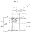
- FIG. 1 illustrates a diagram of a configuration of an organic light-emitting panel according to an embodiment of the invention
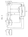
- FIG. 2 illustrates a block diagram of an organic light-emitting display apparatus according to an embodiment of the invention
- FIG. 3 illustrates a block diagram of a configuration of a driving integrated circuit of FIG. 2 according to an embodiment of the invention
- FIG. 4 illustrates a block diagram of a configuration of a voltage conversion unit of FIG. 3 according to an embodiment of the invention
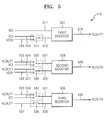
- FIG. 5 illustrates a block diagram of a configuration of a charge pump of FIG. 4 according to an embodiment of the invention
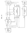
- FIG. 6 illustrates a block diagram of an organic light-emitting display apparatus according to another embodiment of the invention.
- FIG. 7 illustrates a block diagram of a configuration of a driving integrated circuit of FIG. 6 according to an embodiment of the invention
- FIG. 8 illustrates a block diagram of a configuration of a voltage conversion unit of FIG. 7 according to an embodiment of the invention.
- FIG. 9 illustrates a block diagram of configuration in a charge pump of FIG. 8 according to an embodiment of the invention.
- FIG. 1 illustrates a diagram of a configuration of an organic light-emitting panel 100 according to an embodiment of the invention.
- the organic light-emitting panel 100 includes a display unit 120, a scan driver 140, and a source driver 160.
- the display unit 120 includes a plurality of scan lines S1-Sn, a plurality of data lines D1-Dm, and a plurality of pixels P.
- the scan lines S1-Sn are arrayed in rows at regular intervals, and deliver scan signals, respectively.
- the data lines D1-Dm are arrayed in columns at regular intervals, and deliver data signals, respectively.
- the scan lines S1-Sn, and the data lines D1-Dm are matrix-arrayed, and a pixel P is formed in each of intersections between the scan lines S1-Sn, and the data lines D1-Dm.
- the display unit 120 operates according to a normal mode, a low power display mode, and a standby mode of a display apparatus including the organic light-emitting panel 100.
- the display unit 120 receives a power voltage ELVDD and ELVSS, and then allows light-emission of a light-emitting device.
- the display unit 120 receives a first high voltage ELVDD1 and a first low voltage ELVSS1 which are first power voltages, and supplies them to each pixel P.
- the display unit 120 receives a second high voltage ELVDD2 and a second low voltage ELVSS2 which are second power voltages, and supplies them to each pixel P.
- a driving current flows via the light-emitting device from the first high voltage ELVDD1 to the first low voltage ELVSS1, or from the second high voltage ELVDD2 to the second low voltage ELVSS2.
- the driving current allows the light-emission of the light-emitting device, in correspondence to a data signal applied to each pixel P.
- each pixel P may be dedicated to display one of primary colors, or each pixel P may alternately display primary colors according to time.
- a desired color is displayed by spatial or temporal summation of the primary colors.
- the primary colors include red(R), green(G), and blue(B) colors.
- red(R), green(G), and blue(B) colors are alternately displayed in one pixel according to time, so that the color is realized.
- the color is realized by three pixels of R, G, and B pixels.
- each of the three pixels is referred to as a subpixel, and the three sub-pixels are referred to as one pixel.
- R, G, and B pixels may be alternately arrayed in a row direction or a column direction, or may be arrayed in positions that correspond to three vertexes of a triangle.
- the scan driver 140 operates by receiving a first driving voltage Vdd and a second driving voltage Vss in the normal mode, and by receiving a third driving voltage Vdd' and a fourth driving voltage Vss' in the low power display mode.
- the scan driver 140 is connected to the scan lines S1-Sn of the display unit 120.
- the scan driver 140 applies a scan signal, which is configured as a combination of a gate-on voltage and a gate-off voltage, to the scan lines S1-Sn.
- the scan driver 140 may sequentially apply the scan signal to the scan lines S1-Sn. Where the scan signal has the gate-on voltage, a switching transistor connected to a corresponding scan line is turned on. The corresponding scan line is among the scan lines S1-Sn.
- the source driver 160 operates by receiving a first driving voltage Vdd and a second driving voltage Vss in the normal mode, and by receiving a third driving voltage Vdd' and a fourth driving voltage Vss' in the low power display mode.
- the source driver 160 is connected to the data lines D1-Dm of the display unit 120, and applies a data signal indicating a gray scale to the data lines D1-Dm.
- the source driver 160 converts input image data DATA having an input gray scale into a data signal in the form of voltage or current.
- the scan driver 140 and the source driver 160 is in at least one integrated circuit chip, and may be directly mounted on the display unit 120.
- the scan driver 140, the source driver 160, the signal lines S1-Sn and D1-Dm, and a thin film transistor (TFT) may be integrated to the display unit 120.
- the scan driver 140 and the source driver 160 may be integrated into one chip.
- FIG. 2 illustrates a block diagram of an organic light-emitting display apparatus according to another embodiment.
- the organic light-emitting display apparatus includes the organic light-emitting panel 100, a power source unit 200, a power supplying unit 300, and a driving integrated circuit 400.
- the organic light-emitting display apparatus may operate in numerous operation modes, including a normal mode, a low power display mode, and a standby mode.
- the normal mode indicates a general image display mode in which most functions of the organic light-emitting display apparatus are active.
- the low power display mode indicates a power saving mode that reduces the brightness of the organic light-emitting panel 100, or operates only some pixel regions of the organic light-emitting panel 100 to reduce power consumption. For example, where the organic light-emitting display apparatus does not receive a user input during a predetermined time period, the organic light-emitting display apparatus may operate in the low power display mode to reduce power consumption. In another example, where the organic light-emitting display apparatus operates by using a battery and the remaining capacity of the battery is equal to or less than a predetermined level, the organic light-emitting display apparatus may operate in the low power display mode so as to extend available operation time of the organic light-emitting display apparatus. Only some pixel regions may be active in the low power display mode so as to provide functions of a watch, a calendar, a to-do list, etc.
- the standby mode indicates the operation mode in which a power of the organic light-emitting display apparatus remains turned-on, while the organic light-emitting panel 100 does not emit light. For example, in a case where the organic light-emitting display apparatus does not receive a user input during a predetermined time period and the organic light-emitting display apparatus operates in the low power display mode, the organic light-emitting display apparatus may enter the standby mode. In another example, if the organic-light emitting display apparatus does not receive a user input during a predetermined time period and the remaining capacity of a battery is equal to or less than a predetermined level, the organic light-emitting display apparatus may be switched from the normal mode to the standby mode.
- the organic light-emitting panel 100 receives a first high voltage ELVDD1 and a first low voltage ELVSS1 from the power supplying unit 300, and supplies them to each pixel P.
- the organic light-emitting panel 100 receives a second high voltage ELVDD2 and a second low voltage ELVSS2 from the driving integrated circuit 400, and supplies them to each pixel P.
- the organic light-emitting panel 100 receives a first driving voltage Vdd and a second driving voltage Vss from the driving integrated circuit 400 so as to operate a driver (not shown).
- the organic light-emitting panel 100 receives a third driving voltage Vdd' and a fourth driving voltage Vss' from the driving integrated circuit 400.
- Vdd' a third driving voltage
- Vss' a fourth driving voltage
- the power source unit 200 may receive a power from an external power source, and may supply the power to each unit in the organic light-emitting panel 100.
- the power source unit 200 may also supply a power that is charged in a battery to each unit in the organic light-emitting panel 100.
- the power source unit 200 generates an initial voltage required to operate the organic light-emitting display apparatus by using a voltage output from the external power source or from the battery.
- the initial voltage may include a panel power voltage VCI and a logic voltage VDDI.
- the power source unit 200 outputs the panel power voltage VCI to the power supplying unit 300 and the driving integrated circuit 400.
- the power source unit 200 outputs the logic voltage VDDI to the driving integrated circuit 400.
- the logic voltage VDDI is used to drive a logic circuit in the driving integrated circuit 400.
- the power supplying unit 300 receives the panel power voltage VCI from the power source unit 200, converts the panel power voltage VCI, and generates the first high voltage ELVDD1 and the first low voltage ELVSS1.
- the first high voltage ELVDD1 and the first low voltage ELVSS1 allows light-emission of a light-emitting device of the organic light-emitting panel 100.
- the panel power voltage VCI may be regulated and used as an input voltage.
- the panel power voltage VCI may be regulated for generating the first high voltage ELVDD 1 and the first low voltage ELVSS 1.
- the first high voltage ELVDD1 has a positive level
- the first low voltage ELVSS 1 has a negative level.
- the power supplying unit 300 may be electrically connected to the organic light-emitting panel 100 via switching devices SW1 and SW2.
- the first high voltage ELVDD1 and the first low voltage ELVSS1 are input to the organic light-emitting panel 100.
- the power supplying unit 300 may use a direct current DC-to-DC converter as a DC power generator.
- the power supplying unit 300 supplies the first high voltage ELVDD1 and the first low voltage ELVSS1 to the organic light-emitting panel 100.
- the power supplying unit 300 cuts the first high voltage ELVDD1 and the first low voltage ELVSS1.
- the first high voltage ELVDD1 and the first low voltage ELVSS1 are supplied to the organic light-emitting panel 100.
- the power supplying unit 300 uses a low voltage including the panel power voltage VCI as an initial input power. In order to generate a voltage for allowing the light-emission of the light-emitting device, it is necessary to convert the initial input power by boosting or stepping down the initial input power to a desired voltage.
- a structure capable of simultaneously generating the first high voltage ELVDD1 and the first low voltage ELVSS1, with a large voltage difference therebetween, is formed of a plurality of devices. Thus, the structure formed of a plurality of devices increases power consumption.
- the power supplying unit 300 requires a large quiescent current. The power consumed by the quiescent current is greater than power applied to the organic light-emitting panel 100.
- the power supplying unit 300 supplies the first high voltage ELVDD1 and the first low voltage ELVSS 1 to the organic light-emitting panel 100 only when the organic light-emitting panel 100 operates in the normal mode.
- the driving integrated circuit 400 selects a plurality of input voltages according to a display mode of the organic light-emitting panel 100, and generates a voltage from combination of the selected input voltages.
- the voltage is necessary for the organic light-emitting panel 100 in the normal mode or the low power display mode.
- the driving integrated circuit 400 may receive the panel power voltage VCI and the logic voltage VDDI from the power source unit 200, and may generate a voltage from the appropriate combination thereof. The voltage generated is supplied to the organic light-emitting panel 100.
- the driving integrated circuit 400 determines the display mode of the organic light-emitting panel 100.
- the driving integrated circuit 400 outputs a control signal SW that turns on the switching devices SW1 and SW2 when the organic light-emitting panel 100 is in the normal mode.
- the driving integrated circuit outputs a control signal SW that turns off the switching devices SW1 and SW2 when the organic light-emitting panel 100 is in the low power display mode or the standby mode.
- the driving integrated circuit 400 receives the panel power voltage VCI, and generates a first driving voltage Vdd and a second driving voltage Vss for operating each driver of the organic light-emitting panel 100.
- the first driving voltage Vdd and the second driving voltage Vss are supplied to the organic light-emitting panel 100.
- the driving integrated circuit 400 When the organic light-emitting panel 100 is in the low power display mode, the driving integrated circuit 400 generates the second high voltage ELVDD2 and the second low voltage ELVSS2 by using the panel power voltage VCI and the logic voltage VDDI.
- the second high voltage ELVDD2 has a positive level
- the second low voltage ELVSS2 has a negative level.
- a voltage difference between the second high voltage ELVDD2 and the second low voltage ELVSS2 is less then the voltage difference between the first high voltage ELVDD1 and the first low voltage ELVSS1.
- the second high voltage ELVDD2 and the second low voltage ELVSS2 are supplied to the organic light-emitting panel 100.
- the second high voltage ELVDD2 and the second low voltage ELVSS2 may be generated by a combination of the panel power voltage VCI and the logic voltage VDDI.
- the second high voltage ELVDD2 and the second low voltage ELVSS2 may be generated by using a charge pump in the driving integrated circuit 400.
- the driving integrated circuit 400 generates a third driving voltage Vdd' and a fourth driving voltage Vss' by using the panel power voltage VCI and the logic voltage VDDI.
- the third driving voltage Vdd and the fourth driving voltage Vss' may be equivalent to or different from the first driving voltage Vdd and the second driving voltage V ss.
- the driving integrated circuit 400 does not boost or step down only the panel power voltage VCI, but uses both of the panel power voltage VCI and the logic voltage VDDI.
- boosting or stepping down may be decreased or not needed at all. Therefore, for the organic light-emitting panel 100 in the low power display mode, it is possible to generate the optimal low voltage by using a minimum power.
- FIG. 3 illustrates a block diagram of a configuration in the driving integrated circuit 400 of FIG. 2 according to an embodiment.
- the driving integrated circuit 400 includes a mode determination unit 401, a mode control unit 403, a voltage conversion unit 405, and a gamma correction unit 407.
- the mode determination unit 401 determines a display mode of the organic light-emitting panel 100.
- the mode determination unit 401 compares a display mode of the organic light-emitting panel 100 at a previous frame with a display mode of the organic light-emitting panel 100 at a current frame. When the display modes are the same, the power supplying unit 300 and the driving integrated circuit 400 operate in the same manner as the previous frame.
- the mode control unit 403 controls operations of the power supplying unit 300 (refer to FIG. 2 ), the first and second switching devices SW1 and SW2 (refer to FIG. 2 ), and the voltage conversion unit 405 according to the mode determination unit 401.
- the mode control unit 403 controls the operation of the power supplying unit 300 by applying an enable signal to the power supplying unit 300.
- the mode control unit 403 controls the operations of the first and second switching devices SW1 and SW2 by applying a switching signal SW to each of the first and second switching devices SW1 and SW2.
- the voltage conversion unit 405 selects a plurality of input voltages according to the display mode, generates a plurality of output voltages by boosting or stepping down the selected voltages or by combination of the selected voltages, and outputs the generated output voltages to the gamma correction unit 407 and the organic light-emitting panel 100.
- the voltage conversion unit 405 When the organic light-emitting panel 100 operates in the normal mode, the voltage conversion unit 405 generates a first driving voltage Vdd and a second driving voltage Vss by boosting and stepping down a panel power voltage VCI. The voltage conversion unit 405 supplies the first driving voltage Vdd and the second driving voltage Vss to the organic light-emitting panel 100.
- the voltage conversion unit 405 When the organic light-emitting panel 100 operates in the low power display mode, the voltage conversion unit 405 generates a second high voltage ELVDD2 and a second low voltage ELVSS2, and a third driving voltage Vdd' and a fourth driving voltage Vss' by combining the panel power voltage VCI and a logic voltage VDDI. The voltage conversion unit 405 supplies the second high voltage ELVDD2, a second low voltage ELVSS2, a third driving voltage Vdd', and a fourth driving voltage Vss' to the organic light-emitting panel 100.
- the gamma correction unit 407 receives a gamma correction voltage generated by the voltage conversion unit 405, and outputs data DATA.
- the output data DATA has a corrected gamma value.
- the gamma correction unit 407 outputs data DATA to the organic light-emitting panel 100.
- the driving integrated circuit 400 may include a timing control unit (not shown).
- the timing control unit outputs a control signal for controlling each driver of the organic light-emitting panel 100.
- the timing control unit generates a scan control signal and a data control signal.
- the timing control unit applies the scan control signal and the data control signal to a scan driver and a source driver, respectively, of the organic light-emitting panel 100.
- the scan control signal includes a scan start signal and a plurality of clock signals SCLK.
- the the scan start signal indicates a start of a scanning operation.
- the data control signal includes a horizontal synchronization start signal STH and a clock signal.
- the horizontal synchronization start signal STH indicates a transfer of input image data with respect to pixels P in one row.
- FIG. 4 illustrates a block diagram of a configuration in the voltage conversion unit 405 of FIG. 3 according to an embodiment.
- the voltage conversion unit 405 includes a charge pump 415 and an amplifier 425.
- the charge pump 415 boosts an input voltage and then outputs a positive voltage and a negative voltage, which are a multiple of the input voltage.
- the charge pump 415 uses capacitors in the boosting operation.
- the input voltage of the charge pump 415 includes a panel power voltage VCI and a logic voltage VDDI.
- the amplifier 425 amplifies a voltage output from the charge pump 415, and then generates a first driving voltage Vdd and a second driving voltage Vss and Vdd' and Vss'.
- the amplifier 425 amplifies a voltage output from the charge pump 415, and then generates a second high voltage ELVDD2 or a second low voltage ELVSS2.
- the amplifier 425 may separately include an amplifier for generation of a driving voltage, and an amplifier for generation of a power voltage.
- FIG. 5 illustrates a block diagram of a configuration in the charge pump 415 of FIG. 4 according to an embodiment.
- the charge pump 415 includes a first booster 501, a second booster 503, and a third booster 505.
- Each of the boosters 501, 503, and 505 selectively receives an input voltage according to a display mode of the organic light-emitting panel 100, and outputs a voltage according to the display mode.
- the input voltage of each of the boosters 501, 503, and 505 includes a panel power voltage VCI and a logic voltage VDDI.
- the first booster 501 outputs a first output voltage VLOUT1 by using the panel power voltage VCI and the logic voltage VDDI.
- the first booster 501 receives the panel power voltage VCI via a first booster input line 511.
- the first booster 501 receives the panel power voltage VCI or the logic voltage VDDI via a second booster input line 512.
- a switch 513 that is connected to the second booster input line 512 is selectively connected to a panel power voltage input line 514 or a logic voltage input line 515 according to a display mode of the organic light-emitting panel 100.
- the switch 513 When the organic light-emitting panel 100 is in the normal mode, the switch 513 is connected to the panel power voltage input line 514.
- the first booster 501 outputs a first output voltage VLOUT1 via a first output line 516 by using the panel power voltage VCI applied via the first booster input line 511 and the panel power voltage VCI applied via the second booster input line 512.
- the first output voltage VLOUT1 corresponds to 2xVCI, i.e. a double of the panel power voltage VCI.
- the first output voltage VLOUT1 is amplified by the amplifier 425, and output to the gamma correction unit 407.
- the switch 513 When the organic light-emitting panel 100 is in the low power display mode, the switch 513 is connected to the logic voltage input line 515.
- the first booster 501 outputs a first output voltage VLOUT1 via the first output line 516 by using the panel power voltage VCI.
- the panel power voltage VCI is applied via the first booster input line 511 and the logic voltage VDDI is applied via the second booster input line 512.
- the first output voltage VLOUT1 corresponds to VCI+VDDI, i.e. the sum of the panel power voltage VCI and the logic voltage VDDI.
- the first output voltage VLOUT1 is amplified by the amplifier 425, and is output to the gamma correction unit 407.
- the second booster 503 outputs a second output voltage VLOUT2 by using the first output voltage VLOUT1, the panel power voltage VCI, and the logic voltage VDDI.
- the second booster 503 receives the first output voltage VLOUT1 or the panel power voltage VCI via a first booster input line 521.
- a switch 522 that is connected to the first booster input line 521 is selectively connected to a first output voltage input line 523 or a panel power voltage input line 524 according to a display mode of the organic light-emitting panel 100.
- the second booster 503 receives the first output voltage VLOUT1 or the logic voltage VDDI via a second booster input line 525.
- a switch 526 is connected to the second booster input line 525.
- the switch 526 is selectively connected to a first output voltage input line 527 or a logic voltage input line 528 according to a display mode of the organic light-emitting panel 100.
- the switch 522 When the organic light-emitting panel 100 is in the normal mode, the switch 522 is connected to the first output voltage input line 523, and the switch 526 is connected to the first output voltage input line 527.
- the second booster 503 outputs a second output voltage VLOUT2 via a second output line 529 by using the first output voltage VLOUT1 (2xVCI).
- the first output voltage VLOUT1 is applied via the first booster input line 521 and the second booster input line 525.
- the second output voltage VLOUT2 corresponds to 4xVCI, i.e. a quadruple of the panel power voltage VCI.
- the second output voltage VLOUT2 is amplified by the amplifier 425, and output as a first driving voltage Vdd.
- the switch 522 When the organic light-emitting panel 100 is in the low power display mode, the switch 522 is connected to the panel power voltage input line 524, and the switch 526 is connected to the logic voltage input line 528.
- the second booster 503 outputs a second output voltage VLOUT2 via the second output line 529 by using the panel power voltage VCI applied via the first booster input line 521 and the logic voltage VDDI applied via the second booster input line 525, wherein the second output voltage VLOUT2 corresponds to VCI+VDDI that is the sum of the panel power voltage VCI and the logic voltage VDDI.
- the second output voltage VLOUT2 is amplified by the amplifier 425, and then is output as a second high voltage ELVDD2 or a third driving voltage Vdd'.
- the third booster 505 outputs a third output voltage VLOUT3 by using the first output voltage VLOUT1 and the panel power voltage VCI.
- the third booster 505 receives the first output voltage VLOUT1 or the panel power voltage VCI via a first booster input line 531.
- a switch 532 connected to the first booster input line 531, is selectively connected to a first output voltage input line 533 or a panel power voltage input line 534 according to a display mode of the organic light-emitting panel 100.
- the third booster 505 receives the first output voltage VLOUT1 via a second booster input line 535.
- a switch 536 connected to the second booster input line 535, is selectively connected to a first output voltage input line 537 according to a display mode of the organic light-emitting panel 100.
- the switch 532 When the organic light-emitting panel 100 is in the normal mode, the switch 532 is connected to the first output voltage input line 533, and the switch 536 is connected to the first output voltage input line 537.
- the third booster 505 outputs a third output voltage VLOUT3 via a third output line 538 by using the first output voltage VLOUT1 (2xVCI).
- the first output voltage VLOUT1 is applied via the first booster input line 531 and the second booster input line 535.
- the third output voltage VLOUT3 corresponds to -4xVCI, i.e. a negative quadruple of the panel power voltage VCI.
- the third output voltage VLOUT3 is amplified by the amplifier 425, and output as a second driving voltage Vss.
- the switch 532 When the organic light-emitting panel 100 is in the low power display mode, the switch 532 is connected to the panel power voltage input line 534, and the switch 536 is open.
- the third booster 505 outputs a third output voltage VLOUT3 via the third output line 538 by using the panel power voltage VCI.
- the panel power voltage VCI is applied via the first booster input line 531.
- the third output voltage VLOUT3 corresponds to - 1xVCI, i.e. a negative of the panel power voltage VCI.
- the third output voltage VLOUT3 is amplified by the amplifier 425, and output as a second low voltage ELVSS2 or a fourth driving voltage Vss'.
- FIG. 6 illustrates a block diagram of an organic light-emitting display apparatus according to another embodiment.
- the organic light-emitting display apparatus includes the organic light-emitting panel 100, a power source unit 250, a power supplying unit 350, a driving integrated circuit 450, a touch integrated circuit 600, and a touch sensor 650.
- the embodiment of FIG. 6 is different from the embodiment of FIG. 2 in that the embodiment of FIG. 6 further includes the touch integrated circuit 600 and the touch sensor 650.
- the embodiment of FIG. 6 uses a touch voltage VDD as an input voltage for generating a power voltage of the driving integrated circuit 450, instead of using a logic voltage VDDI in the embodiment of FIG. 2 .
- the organic light-emitting panel 100 When the organic light-emitting panel 100 operates in a normal mode, the organic light-emitting panel 100 receives a first high voltage ELVDD 1 and a first low voltage ELVSS1 from the power supplying unit 350. The organic light-emitting panel 100 supplies the first high voltage ELVDD1 and a first low voltage ELVSS1 to each pixel. When the organic light-emitting panel 100 operates in a low power display mode, the organic light-emitting panel 100 receives a second high voltage ELVDD2 and a second low voltage ELVSS2 from the driving integrated circuit 450. The organic light-emitting panel 100 supplies the second high voltage ELVDD2 and the second low voltage ELVSS2 to each pixel.
- the organic light-emitting panel 100 receives a first driving voltage Vdd and a second driving voltage Vss for operating each driver from the driving integrated circuit 450.
- the organic light-emitting panel 100 receives a third driving voltage Vdd' and a fourth driving voltage Vss' from the driving integrated circuit 450.
- the configuration in the organic light-emitting panel 100 is described above with reference to FIG. 1 .
- the power source unit 250 may receive power from an external power source, and may supply the power to each unit in the organic light-emitting panel 100.
- the power source unit 250 may supply a power that is charged in a battery to each unit in the organic light-emitting panel 100.
- the power source unit 250 generates an initial voltage required to operate the organic light-emitting display apparatus by using a voltage output from the external power source or from the battery.
- the initial voltage may include a panel power voltage VCI, a logic voltage VDDI, and a touch voltage VDD.
- the power source unit 250 outputs the panel power voltage VCI to the power supplying unit 350 and the driving integrated circuit 450, and outputs the logic voltage VDDI to the driving integrated circuit 450.
- the logic voltage VDDI is used to drive a logic circuit in the driving integrated circuit 450.
- the power source unit 250 outputs the touch voltage VDD to the driving integrated circuit 450 and the touch integrated circuit 600.
- the touch voltage VDD is used to drive the touch integrated circuit 600.
- the power supplying unit 350 receives the panel power voltage VCI from the power source unit 250, converts the panel power voltage VCI, and then generates the first high voltage ELVDD1 and the first low voltage ELVSS1.
- the generation of the first high voltage ELVDD1 and the first low voltage ELVSS1 allows for light-emission of a light-emitting device of the organic light-emitting panel 100.
- the panel power voltage VCI may be regulated.
- the power voltage VCI may be used as an input voltage for generating the first high voltage ELVDD1 and the first low voltage ELVSS1.
- the first high voltage ELVDD1 has a positive level
- the first low voltage ELVSS1 has a negative level.
- the power supplying unit 350 may be electrically connected to the organic light-emitting panel 100 via switching devices SW1 and SW2.
- the first high voltage ELVDD1 and the first low voltage ELVSS1 are input to the organic light-emitting panel 100.
- the power supplying unit 350 may use a DC-to-DC converter as a DC power generator.
- the power supplying unit 350 supplies the first high voltage ELVDD1 and the first low voltage ELVSS 1 to the organic light-emitting panel 100.
- the power supplying unit 350 cuts the first high voltage ELVDD1 and the first low voltage ELVSS1.
- the first high voltage ELVDD1 and the first low voltage ELVSS1 are supplied to the organic light-emitting panel 100.
- the driving integrated circuit 450 selects a plurality of input voltages according to a display mode of the organic light-emitting panel 100.
- the driving integrated circuit 450 generates a voltage from combination of the selected input voltages, wherein the voltage is necessary for the organic light-emitting panel 100 in the normal mode or the low power display mode.
- the driving integrated circuit 450 may receive the panel power voltage VCI, the logic voltage VDDI, and the touch voltage VDD from the power source unit 250.
- the driving circuit 450 may generate a voltage from the appropriate combination thereof.
- the generated voltage is for the organic light-emitting panel 100.
- the driving integrated circuit 450 determines the display mode of the organic light-emitting panel 100.
- the driving integrated circuit 450 outputs a control signal SW that turns on the switching devices SW1 and SW2 when the organic light-emitting panel 100 is in the normal mode.
- the driving integrated circuit 450 turns off the switching devices SW1 and SW2 when the organic light-emitting panel 100 is in the low power display mode or the standby mode.
- the driving integrated circuit 450 receives the panel power voltage VCI, and generates a first driving voltage Vdd and a second driving voltage Vss for operating each driver of the organic light-emitting panel 100.
- the first driving voltage Vdd and the second driving voltage Vss are supplied to the organic light-emitting panel 100.
- the driving integrated circuit 450 When the organic light-emitting panel 100 is in the low power display mode, the driving integrated circuit 450 generates the second high voltage ELVDD2 and the second low voltage ELVSS2 by using the panel power voltage VCI and the touch voltage VDD.
- the second high voltage ELVDD2 has a positive level
- the second low voltage ELVSS2 has a negative level.
- a voltage difference between the second high voltage ELVDD2 and the second low voltage ELVSS2 is less then a voltage difference between the first high voltage ELVDD1 and the first low voltage ELVSS1.
- the second high voltage ELVDD2 and the second low voltage ELVSS2 are supplied to the organic light-emitting panel 100.
- the second high voltage ELVDD2 and the second low voltage ELVSS2 may be generated by combining the panel power voltage VCI and the touch voltage VDD by using a charge pump in the driving integrated circuit 450. Also, the driving integrated circuit 450 generates a third driving voltage Vdd' and a fourth driving voltage Vss' by using the panel power voltage VCI and the touch voltage VDD. The third driving voltage Vdd and the fourth driving voltage Vss may be equivalent to or different from the first driving voltage Vdd and the second driving voltage Vss.
- the touch integrated circuit 600 receives the touch voltage VDD from the power source unit 250, and generates a driving signal for operating the touch sensor 650.
- the touch sensor 650 receives the driving signal from the touch integrated circuit 600, and detects a contact by a user or an object.
- the touch sensor 650 may be separately arranged on the organic light-emitting panel 100, or may be embedded in a pixel array.
- the driving integrated circuit 450 does not boost or step down only the panel power voltage VCI, but uses all of the panel power voltage VCI, the logic voltage VDDI, and the touch voltage VDD, so that boosted or stepped down voltages may be decreased. Thus, it is possible to generate the low voltage by using minimum power.
- the low voltage is optimal for the organic light-emitting panel 100 in the low power display mode.
- FIG. 7 illustrates a block diagram of a configuration in the driving integrated circuit 450 of FIG. 6 according to an embodiment.
- the driving integrated circuit 450 includes a mode determination unit 471, a mode control unit 473, a voltage conversion unit 475, and a gamma correction unit 477.
- the mode determination unit 471 determines a display mode of the organic light-emitting panel 100.
- the mode determination unit 471 compares a display mode of the organic light-emitting panel 100 at a previous frame with a display mode of the organic light-emitting panel 100 at a current frame. When the display modes are the same, the power supplying unit 350 and the driving integrated circuit 450 operate in the same manner as the previous frame.
- the mode control unit 473 controls operations of the power supplying unit 350, the first and second switching devices SW1 and SW2 (refer to FIG. 6 ), and the voltage conversion unit 475 according to the mode determination unit 471.
- the mode control unit 473 controls the operation of the power supplying unit 350 by applying an enable signal to the power supplying unit 350.
- the mode control unit 473 controls the operations of the first and second switching devices SW1 and SW2 by applying a switching signal SW to each of the first and second switching devices SW1 and SW2.
- the voltage conversion unit 475 selects a plurality of input voltages according to the display mode, generates a plurality of output voltages by boosting or stepping down the selected voltages or by combining the selected voltages, and outputs the generated output voltages to the gamma correction unit 477 and the organic light-emitting panel 100.
- the voltage conversion unit 475 When the organic light-emitting panel 100 operates in the normal mode, the voltage conversion unit 475 generates a first driving voltage Vdd and a second driving voltage Vss by boosting and stepping down a panel power voltage VCI. The voltage conversion unit 475 supplies the first driving voltage Vdd and the second driving voltage Vss to the organic light-emitting panel 100.
- the voltage conversion unit 475 When the organic light-emitting panel 100 operates in the low power display mode, the voltage conversion unit 475 generates a second high voltage ELVDD2 and a second low voltage ELVSS2, and a third driving voltage Vdd' and a fourth driving voltage Vss' by combining the panel power voltage VCI, a logic voltage VDDI, and a touch voltage VDD.
- the organic light-emitting panel 100 supplies the second high voltage ELVDD2, the second low voltage ELVSS2, the third driving voltage Vdd', and the fourth driving voltage Vss' to the organic light-emitting panel 100.
- the gamma correction unit 477 receives a gamma correction voltage generated by the voltage conversion unit 475, and outputs data DATA.
- the output data DATA has a corrected gamma value.
- the output data DATA is supplied to the organic light-emitting panel 100.
- the driving integrated circuit 450 may include a timing control unit (not shown).
- the timing control unit outputs a control signal for controlling each driver of the organic light-emitting panel 100.
- the timing control unit generates a scan control signal and a data control signal, and applies the scan control signal and the data control signal to a scan driver and a source driver, respectively, of the organic light-emitting panel 100.
- the scan control signal includes a scan start signal and a plurality of clock signals SCLK.
- the scan start signal indicates a start of a scanning operation.
- the data control signal includes a horizontal synchronization start signal STH and a clock signal.
- the horizontal synchronization start signal STH indicates a transfer of input image data with respect to pixels P in one row.
- FIG. 8 illustrates a block diagram of a configuration in the voltage conversion unit 475 of FIG. 7 .
- the voltage conversion unit 475 includes a charge pump 491 and an amplifier 495.
- the charge pump 491 boosts an input voltage and then outputs a positive voltage and a negative voltage, which are a multiple of the input voltage.
- the charge pump 491 uses capacitors in the boosting operation.
- the input voltage of the charge pump 415 includes a panel power voltage VCI and a touch voltage VDD.
- the amplifier 495 amplifies a voltage output from the charge pump 491, and then generates a first driving voltage Vdd and a second driving voltage Vss.
- the amplifier 495 amplifies a voltage output from the charge pump 491, and then generates a second high voltage ELVDD2 or a second low voltage ELVSS2.
- the amplifier 495 may separately include an amplifier for generation of a driving voltage, and an amplifier for generation of a power voltage.
- FIG. 9 illustrates a block diagram of a configuration of the charge pump 491 of FIG. 8 in accordance with an embodiment.
- the charge pump 491 includes a first booster 901, a second booster 903, and a third booster 905.
- Each of the boosters 901, 903, and 905 selectively receives an input voltage according to a display mode of the organic light-emitting panel 100, and outputs a voltage according to the display mode.
- the input voltage of each of the boosters 901, 903, and 905 includes a panel power voltage VCI and a touch voltage VDD.
- the first booster 901 outputs a first output voltage VLOUT1 by using the panel power voltage VCI and the touch voltage VDD.
- the first booster 901 receives the panel power voltage VCI or the touch voltage VDD via a first booster input line 911.
- a switch 912 connected to the first booster input line 911, is selectively connected to a panel power voltage input line 913 or a touch voltage input line 914 according to a display mode of the organic light-emitting panel 100.
- the first booster 901 receives the panel power voltage VCI or the touch voltage VDD via a second booster input line 915.
- a switch 916, connected to the second booster input line 915 is selectively connected to a panel power voltage input line 917 or a touch voltage input line 918 according to the display mode of the organic light-emitting panel 100.
- the switch 912 When the organic light-emitting panel 100 is in the normal mode, the switch 912 is connected to the panel power voltage input line 913, and the switch 916 is connected to the panel power voltage input line 917.
- the first booster 901 outputs a first output voltage VLOUT1, via a first output line 919, by using the panel power voltage VCI applied via the first booster input line 911 and the panel power voltage VCI applied via the second booster input line 915.
- the first output voltage VLOUT1 corresponds to 2xVCI, i.e. double of the panel power voltage VCI.
- the first output voltage VLOUT1 is amplified by the amplifier 495, and output to the gamma correction unit 477.
- the switch 912 When the organic light-emitting panel 100 is in the low power display mode, the switch 912 is connected to the touch voltage input line 914.
- the switch 916 is connected to the touch voltage input line 918.
- the first booster 901 outputs a first output voltage VLOUT1 via the first output line 919.
- the first booster 901 outputs a first output voltage VLOUT1 by using the touch voltage VDD applied via the first booster input line 911 and the touch voltage VDD applied via the second booster input line 915.
- the first output voltage VLOUT1 corresponds to 2xVDD, i.e. double of the touch voltage VDD.
- the first output voltage VLOUT1 is amplified by the amplifier 495, and output to the gamma correction unit 477.
- the second booster 903 outputs a second output voltage VLOUT2 by using the first output voltage VLOUT1.
- the second booster 903 receives the first output voltage VLOUT1 via a first booster input line 921 and a second booster input line 922.
- the second booster 903 When the organic light-emitting panel 100 is in the normal mode, the second booster 903 outputs the second output voltage VLOUT2 via a second output line 923.
- the second output voltage VLOUT2 corresponds to 4xVCI, i.e. the sum of the first output voltage VLOUT1 (2xVCI) applied via the first booster input line 921 and the first output voltage VLOUT1 (2xVCI) applied via the second booster input line 922.
- the second output voltage VLOUT2 is amplified by the amplifier 495, and output as a first driving voltage Vdd.
- the second booster 903 When the organic light-emitting panel 100 is in the low power display mode, the second booster 903 outputs a second output voltage VLOUT2 via the second output line 923.
- the second output voltage VLOUT2 corresponds to 4xVDD, i.e. the sum of the first output voltage VLOUT1 (2xVDD) applied via the first booster input line 921 and the first output voltage VLOUT1 (2xVDD) applied via the second booster input line 922.
- the second output voltage VLOUT2 is amplified by the amplifier 495, and output as a second high voltage ELVDD2 or a third driving voltage Vdd'.
- the third booster 905 outputs a third output voltage VLOUT3 by using the first output voltage VLOUT1 and the touch voltage VDD.
- the third booster 905 receives the first output voltage VLOUT1 or the touch voltage VDD via a first booster input line 931.
- a switch 932 connected to the first booster input line 931, is selectively connected to a first output voltage input line 933 or a touch voltage input line 934 according to a display mode of the organic light-emitting panel 100.
- the third booster 905 receives the first output voltage VLOUT1 via a second booster input line 935.
- a switch 93 6, connected to the second booster input line 93 5, is selectively connected to a first output voltage input line 937 according to a display mode of the organic light-emitting panel 100.
- the switch 932 When the organic light-emitting panel 100 is in the normal mode, the switch 932 is connected to the first output voltage input line 93 3, and the switch 93 6 is connected to the first output voltage input line 937.
- the third booster 905 outputs a third output voltage VLOUT3 via a third output line 938 by using the first output voltage VLOUT1 (2xVCI).
- the first output voltage VLOUT1 is applied via each of the first booster input line 931 and the second booster input line 935.
- the third output voltage VLOUT3 corresponds to -4xVCI, i.e. a negative quadruple of the panel power voltage VCI.
- the third output voltage VLOUT3 is amplified by the amplifier 495, and output as a second driving voltage Vss.
- the switch 932 When the organic light-emitting panel 100 is in the low power display mode, the switch 932 is connected to the touch voltage input line 934, and the switch 936 is open.
- the third booster 905 outputs a third output voltage VLOUT3 via the third output line 938 by using the touch voltage VDD that is applied via the first booster input line 931.
- the third output voltage VLOUT3 corresponds to -1xVDD, i.e. a negative of the touch voltage VDD.
- the third output voltage VLOUT3 is amplified by the amplifier 495, and output as a second low voltage ELVSS2 or a fourth driving voltage Vss'.
- a voltage for the organic light-emitting panel 100 is generated by using the logic voltage VDDI or the touch voltage VDD as the input voltage.
- Generation of the voltage for the organic light-emitting panel 100 is not limited thereto.
- the voltage for the organic light-emitting panel 100 in the low power display mode may vary according to a characteristic of a panel, so that the input voltage may be set from combination of the panel power voltage VCI, the logic voltage VDDI, and the touch voltage VDD, according to a low voltage necessary for the organic light-emitting panel 100 in the low power display mode.
- the driving integrated circuit may select the panel power voltage VCI having 3.7V and the touch voltage VDD having 2.8V as input voltages. Compared to a scenario in which 6.5V is generated by additionally boosting the panel power voltage VCI or the logic voltage VDDI, power consumption is reduced.
- voltages e.g., a voltage from a camera module included in a display apparatus
- a power source unit e.g., a voltage from a camera module included in a display apparatus
- the organic light-emitting display apparatus is described as an example in the aforementioned embodiments, but the display apparatus according to the one or more embodiments of the present invention is not limited thereto and thus may include various types of display apparatuses including the organic light-emitting display apparatus, a liquid crystal display (LCD) device, a field emission display (FED) device, or the like.
- LCD liquid crystal display
- FED field emission display
- a power voltage for a panel is supplied from the driving integrated circuit, so that power consumption in the power supplying unit may be reduced.
- the power voltage for the panel is generated by using combination of other voltages as well as the panel power voltage, so that power consumption required in voltage generation may be reduced.
Landscapes
- Engineering & Computer Science (AREA)
- Physics & Mathematics (AREA)
- Computer Hardware Design (AREA)
- General Physics & Mathematics (AREA)
- Theoretical Computer Science (AREA)
- Control Of Indicators Other Than Cathode Ray Tubes (AREA)
- Control Of El Displays (AREA)
- Electroluminescent Light Sources (AREA)
Abstract
Description
- The present invention relates to a display apparatus that reduces power consumption in a low power display mode, and a power supplying method performed by the display apparatus,
- A display apparatus displays an image corresponding to an input image by applying a scan signal and a data voltage to each of a plurality of pixels. Each of the pixels operates by receiving at least one power voltage. For this operation, the display apparatus generates at least one power voltage from an external power source. A display panel receives at least one power voltage.
- The display apparatus is applied to mobile equipment, such as mobile phones, digital cameras, etc. For mobile equipment, it becomes important to reduce power consumption of the display apparatus. In general, mobile equipment operates by using a battery. It is important to extend a battery use time for mobile equipment by reducing consumption of power stored in the battery. However, the display apparatus in mobile equipment requires high power consumption. There is a demand for decreasing power consumption in the display apparatus.
- The present invention sets out to provide a display apparatus and a power supplying method performed thereof, which substantially overcome one or more of the problems due to the limitations and disadvantages of the related art.
- It is therefore a feature of an embodiment to provide a display apparatus capable of reducing power consumption.
- It is therefore another feature of an embodiment to provide a power supplying method capable of reducing power consumption.
- At least one of the above and other features and advantages may be realized by providing a display apparatus including a panel that operates in a normal mode or a low power display mode; a power supplying unit that outputs a first high voltage and a first low voltage to the panel in the normal mode, wherein the first high voltage and the first low voltage are first power voltages; and a driving integrated circuit that selects at least one input voltage from among a plurality of input voltages according to a display mode, and that outputs a second high voltage and a second low voltage to the panel in the low power display mode, wherein the second high voltage and the second low voltage are second power voltages generated based on the selected at least one input voltage.
- The power supplying unit may generate the first power voltages based on a panel power voltage, and the driving integrated circuit may generate the second power voltages based on a panel power voltage and a logic voltage.
- A difference between the second high voltage and the second low voltage may be less then a difference between the first high voltage and the first low voltage.
- The driving integrated circuit may include a mode determination unit that determines the display mode; and a voltage conversion unit that generates a first driving voltage and a second driving voltage based on the panel power voltage in the normal mode, and that generates the second power voltages, a third driving voltage, and a fourth driving voltage based on the panel power voltage and the logic voltage in the low power display mode.
- The voltage conversion unit may include a charge pump that boosts an input voltage and then outputs a positive voltage and a negative voltage that are a multiple of the input voltage; and an amplifier that amplifies the positive voltage and the negative voltage output from the charge pump, and then generates the first driving voltage, the second driving voltage, the second power voltages, the third driving voltage, and the fourth driving voltage.
- The charge pump may include a first booster that outputs a positive first output voltage boosted to a predetermined level by using panel power voltages input via a first input line and a second input line in the normal mode, and that outputs a positive first output voltage boosted to a predetermined level by using the panel power voltage input via the first input line, and a logic voltage input via the second input line in the low power display mode; a second booster that outputs a positive second output voltage boosted to a predetermined level by using the positive first output voltages input via a first input line and a second input line in the normal mode, and that outputs a positive second output voltage boosted to a predetermined level by using the panel power voltage input via the first input line, and a logic voltage input via the second input line in the low power display mode; and a third booster that outputs a negative third output voltage stepped down to a predetermined level by using the positive first output voltages input via a first input line and a second input line in the normal mode, and that outputs a negative third output voltage stepped down to a predetermined level by using the panel power voltage input via the first input line in the low power display mode.
- The driving integrated circuit may further include a gamma correction unit that receives a voltage as a gamma correction voltage, wherein the voltage is obtained by amplifying the first output voltage.
- The display apparatus may further include a touch integrated circuit that receives a touch voltage and then generates a driving signal for operating a touch sensor, and the driving integrated circuit may generate the second power voltages based on the touch voltage.
- The driving integrated circuit may include a mode determination unit that determines the display mode; and a voltage conversion unit that generates a first driving voltage and a second driving voltage based on the panel power voltage in the normal mode, and that generates the second power voltages, a third driving voltage, and a fourth driving voltage based on the touch voltage in the low power display mode.
- The charge pump may include a first booster that outputs a positive first output voltage boosted to a predetermined level by using panel power voltages input via a first input line and a second input line in the normal mode, and that outputs a positive first output voltage boosted to a predetermined level by using touch voltages input via the first input line and the second input line in the low power display mode; a second booster that outputs a positive second output voltage boosted to a predetermined level by using the positive first output voltages input via a first input line and a second input line in the normal mode, and that outputs a positive second output voltage boosted to a predetermined level by using the positive first output voltages input via the first input line and the second input line in the low power display mode; and a third booster that outputs a negative third output voltage stepped down to a predetermined level by using the positive first output voltages input via a first input line and a second input line in the normal mode, and that outputs a negative third output voltage stepped down to a predetermined level by using a touch voltage input via the first input line in the low power display mode.
- The display apparatus may further include a first switching device that is arranged between the power supplying unit and the panel, and that cuts the first high voltage; and a second switching device that is arranged between the power supplying unit and the panel, and that cuts the first low voltage.
- At least one of the above and other features and advantages may also be realized by providing a power supplying method performed by a display apparatus so as to drive a panel that operates in a normal mode and a low power display mode, the power supplying method including the operations of, supplying a first high voltage and a first low voltage by a power supplying unit in the normal mode, the first high voltage and the first low voltage are first power voltages to the panel; and selecting at least one input voltage from among a plurality of input voltages by a driving integrated circuit in the low power display mode, and outputting a second high voltage and a second low voltage to the panel, wherein the second high voltage and the second low voltage are second power voltages generated based on the selected at least one input voltage.
- At least some of the above and other features of the invention are set out in the claims.
- The above and other features and advantages will become more apparent to those of ordinary skill in the art which is given upon making reference to the following description by way of example and with reference to the attached drawings, in which:
-
FIG. 1 illustrates a diagram of a configuration of an organic light-emitting panel according to an embodiment of the invention; -
FIG. 2 illustrates a block diagram of an organic light-emitting display apparatus according to an embodiment of the invention; -
FIG. 3 illustrates a block diagram of a configuration of a driving integrated circuit ofFIG. 2 according to an embodiment of the invention; -
FIG. 4 illustrates a block diagram of a configuration of a voltage conversion unit ofFIG. 3 according to an embodiment of the invention; -
FIG. 5 illustrates a block diagram of a configuration of a charge pump ofFIG. 4 according to an embodiment of the invention; -
FIG. 6 illustrates a block diagram of an organic light-emitting display apparatus according to another embodiment of the invention; -
FIG. 7 illustrates a block diagram of a configuration of a driving integrated circuit ofFIG. 6 according to an embodiment of the invention; -
FIG. 8 illustrates a block diagram of a configuration of a voltage conversion unit ofFIG. 7 according to an embodiment of the invention; and -
FIG. 9 illustrates a block diagram of configuration in a charge pump ofFIG. 8 according to an embodiment of the invention. - Example embodiments will now be described more fully hereinafter with reference to the accompanying drawings; however, the invention may be embodied in different forms and should not be construed as limited to the embodiments set forth herein. Rather, these embodiments are provided so that this disclosure will be thorough and complete, and will fully convey the scope of the invention to those skilled in the art. Like reference numerals in the drawings denote like elements. In the following description, well-known functions or constructions are not described in detail, as they would obscure the embodiments with unnecessary detail.
-
FIG. 1 illustrates a diagram of a configuration of an organic light-emitting panel 100 according to an embodiment of the invention. Referring toFIG. 1 , the organic light-emitting panel 100 includes adisplay unit 120, ascan driver 140, and asource driver 160. - The
display unit 120 includes a plurality of scan lines S1-Sn, a plurality of data lines D1-Dm, and a plurality of pixels P. The scan lines S1-Sn are arrayed in rows at regular intervals, and deliver scan signals, respectively. The data lines D1-Dm are arrayed in columns at regular intervals, and deliver data signals, respectively. The scan lines S1-Sn, and the data lines D1-Dm are matrix-arrayed, and a pixel P is formed in each of intersections between the scan lines S1-Sn, and the data lines D1-Dm. - The
display unit 120 operates according to a normal mode, a low power display mode, and a standby mode of a display apparatus including the organic light-emitting panel 100. Thedisplay unit 120 receives a power voltage ELVDD and ELVSS, and then allows light-emission of a light-emitting device. In the normal mode, thedisplay unit 120 receives a first high voltage ELVDD1 and a first low voltage ELVSS1 which are first power voltages, and supplies them to each pixel P. In the low power display mode, thedisplay unit 120 receives a second high voltage ELVDD2 and a second low voltage ELVSS2 which are second power voltages, and supplies them to each pixel P. In each pixel P, a driving current flows via the light-emitting device from the first high voltage ELVDD1 to the first low voltage ELVSS1, or from the second high voltage ELVDD2 to the second low voltage ELVSS2. The driving current allows the light-emission of the light-emitting device, in correspondence to a data signal applied to each pixel P. - In order to realize a color display, each pixel P may be dedicated to display one of primary colors, or each pixel P may alternately display primary colors according to time. A desired color is displayed by spatial or temporal summation of the primary colors. Examples of the primary colors include red(R), green(G), and blue(B) colors. Where a color is displayed by the temporal summation, red(R), green(G), and blue(B) colors are alternately displayed in one pixel according to time, so that the color is realized. Where a color is displayed by the spatial summation, the color is realized by three pixels of R, G, and B pixels. Thus, each of the three pixels is referred to as a subpixel, and the three sub-pixels are referred to as one pixel. Where a color is displayed by the spatial summation, R, G, and B pixels may be alternately arrayed in a row direction or a column direction, or may be arrayed in positions that correspond to three vertexes of a triangle.
- The
scan driver 140 operates by receiving a first driving voltage Vdd and a second driving voltage Vss in the normal mode, and by receiving a third driving voltage Vdd' and a fourth driving voltage Vss' in the low power display mode. Thescan driver 140 is connected to the scan lines S1-Sn of thedisplay unit 120. Thescan driver 140 applies a scan signal, which is configured as a combination of a gate-on voltage and a gate-off voltage, to the scan lines S1-Sn. Thescan driver 140 may sequentially apply the scan signal to the scan lines S1-Sn. Where the scan signal has the gate-on voltage, a switching transistor connected to a corresponding scan line is turned on. The corresponding scan line is among the scan lines S1-Sn. - The
source driver 160 operates by receiving a first driving voltage Vdd and a second driving voltage Vss in the normal mode, and by receiving a third driving voltage Vdd' and a fourth driving voltage Vss' in the low power display mode. Thesource driver 160 is connected to the data lines D1-Dm of thedisplay unit 120, and applies a data signal indicating a gray scale to the data lines D1-Dm. Thesource driver 160 converts input image data DATA having an input gray scale into a data signal in the form of voltage or current. - The
scan driver 140 and thesource driver 160 is in at least one integrated circuit chip, and may be directly mounted on thedisplay unit 120. In another embodiment, thescan driver 140, thesource driver 160, the signal lines S1-Sn and D1-Dm, and a thin film transistor (TFT) may be integrated to thedisplay unit 120. Thescan driver 140 and thesource driver 160 may be integrated into one chip. -
FIG. 2 illustrates a block diagram of an organic light-emitting display apparatus according to another embodiment. Referring toFIG. 2 , the organic light-emitting display apparatus includes the organic light-emittingpanel 100, apower source unit 200, apower supplying unit 300, and a drivingintegrated circuit 400. - The organic light-emitting display apparatus may operate in numerous operation modes, including a normal mode, a low power display mode, and a standby mode.
- The normal mode indicates a general image display mode in which most functions of the organic light-emitting display apparatus are active.
- The low power display mode indicates a power saving mode that reduces the brightness of the organic light-emitting
panel 100, or operates only some pixel regions of the organic light-emittingpanel 100 to reduce power consumption. For example, where the organic light-emitting display apparatus does not receive a user input during a predetermined time period, the organic light-emitting display apparatus may operate in the low power display mode to reduce power consumption. In another example, where the organic light-emitting display apparatus operates by using a battery and the remaining capacity of the battery is equal to or less than a predetermined level, the organic light-emitting display apparatus may operate in the low power display mode so as to extend available operation time of the organic light-emitting display apparatus. Only some pixel regions may be active in the low power display mode so as to provide functions of a watch, a calendar, a to-do list, etc. - The standby mode indicates the operation mode in which a power of the organic light-emitting display apparatus remains turned-on, while the organic light-emitting
panel 100 does not emit light. For example, in a case where the organic light-emitting display apparatus does not receive a user input during a predetermined time period and the organic light-emitting display apparatus operates in the low power display mode, the organic light-emitting display apparatus may enter the standby mode. In another example, if the organic-light emitting display apparatus does not receive a user input during a predetermined time period and the remaining capacity of a battery is equal to or less than a predetermined level, the organic light-emitting display apparatus may be switched from the normal mode to the standby mode. - In the normal mode, the organic light-emitting
panel 100 receives a first high voltage ELVDD1 and a first low voltage ELVSS1 from thepower supplying unit 300, and supplies them to each pixel P. In the low power display mode, the organic light-emittingpanel 100 receives a second high voltage ELVDD2 and a second low voltage ELVSS2 from the drivingintegrated circuit 400, and supplies them to each pixel P. In the normal mode, the organic light-emittingpanel 100 receives a first driving voltage Vdd and a second driving voltage Vss from the drivingintegrated circuit 400 so as to operate a driver (not shown). In the low power display mode, the organic light-emittingpanel 100 receives a third driving voltage Vdd' and a fourth driving voltage Vss' from the drivingintegrated circuit 400. A configuration of the organic light-emittingpanel 100 is described above with reference toFIG. 1 . - The
power source unit 200 may receive a power from an external power source, and may supply the power to each unit in the organic light-emittingpanel 100. Thepower source unit 200 may also supply a power that is charged in a battery to each unit in the organic light-emittingpanel 100. Thepower source unit 200 generates an initial voltage required to operate the organic light-emitting display apparatus by using a voltage output from the external power source or from the battery. The initial voltage may include a panel power voltage VCI and a logic voltage VDDI. Thepower source unit 200 outputs the panel power voltage VCI to thepower supplying unit 300 and the drivingintegrated circuit 400. Thepower source unit 200 outputs the logic voltage VDDI to the drivingintegrated circuit 400. The logic voltage VDDI is used to drive a logic circuit in the drivingintegrated circuit 400. - The
power supplying unit 300 receives the panel power voltage VCI from thepower source unit 200, converts the panel power voltage VCI, and generates the first high voltage ELVDD1 and the first low voltage ELVSS1. The first high voltage ELVDD1 and the first low voltage ELVSS1 allows light-emission of a light-emitting device of the organic light-emittingpanel 100. The panel power voltage VCI may be regulated and used as an input voltage. The panel power voltage VCI may be regulated for generating the firsthigh voltage ELVDD 1 and the firstlow voltage ELVSS 1. The first high voltage ELVDD1 has a positive level, and the firstlow voltage ELVSS 1 has a negative level. Thepower supplying unit 300 may be electrically connected to the organic light-emittingpanel 100 via switching devices SW1 and SW2. The first high voltage ELVDD1 and the first low voltage ELVSS1 are input to the organic light-emittingpanel 100. Thepower supplying unit 300 may use a direct current DC-to-DC converter as a DC power generator. - When the organic light-emitting
panel 100 operates in the normal mode, thepower supplying unit 300 supplies the first high voltage ELVDD1 and the first low voltage ELVSS1 to the organic light-emittingpanel 100. When the organic light-emittingpanel 100 operates in the low power display mode or the standby mode, thepower supplying unit 300 cuts the first high voltage ELVDD1 and the first low voltage ELVSS1. The first high voltage ELVDD1 and the first low voltage ELVSS1 are supplied to the organic light-emittingpanel 100. - The
power supplying unit 300 uses a low voltage including the panel power voltage VCI as an initial input power. In order to generate a voltage for allowing the light-emission of the light-emitting device, it is necessary to convert the initial input power by boosting or stepping down the initial input power to a desired voltage. A structure capable of simultaneously generating the first high voltage ELVDD1 and the first low voltage ELVSS1, with a large voltage difference therebetween, is formed of a plurality of devices. Thus, the structure formed of a plurality of devices increases power consumption. When the organic light-emittingpanel 100 operates in the low power display mode, thepower supplying unit 300 requires a large quiescent current. The power consumed by the quiescent current is greater than power applied to the organic light-emittingpanel 100. In order to prevent the quiescent current consumed when the organic light-emittingpanel 100 operates in the low power display mode, thepower supplying unit 300 supplies the first high voltage ELVDD1 and the firstlow voltage ELVSS 1 to the organic light-emittingpanel 100 only when the organic light-emittingpanel 100 operates in the normal mode. - The driving
integrated circuit 400 selects a plurality of input voltages according to a display mode of the organic light-emittingpanel 100, and generates a voltage from combination of the selected input voltages. The voltage is necessary for the organic light-emittingpanel 100 in the normal mode or the low power display mode. For example, the drivingintegrated circuit 400 may receive the panel power voltage VCI and the logic voltage VDDI from thepower source unit 200, and may generate a voltage from the appropriate combination thereof. The voltage generated is supplied to the organic light-emittingpanel 100. The drivingintegrated circuit 400 determines the display mode of the organic light-emittingpanel 100. The drivingintegrated circuit 400 outputs a control signal SW that turns on the switching devices SW1 and SW2 when the organic light-emittingpanel 100 is in the normal mode. The driving integrated circuit outputs a control signal SW that turns off the switching devices SW1 and SW2 when the organic light-emittingpanel 100 is in the low power display mode or the standby mode. - When the organic light-emitting
panel 100 is in the normal mode, the drivingintegrated circuit 400 receives the panel power voltage VCI, and generates a first driving voltage Vdd and a second driving voltage Vss for operating each driver of the organic light-emittingpanel 100. The first driving voltage Vdd and the second driving voltage Vss are supplied to the organic light-emittingpanel 100. - When the organic light-emitting
panel 100 is in the low power display mode, the drivingintegrated circuit 400 generates the second high voltage ELVDD2 and the second low voltage ELVSS2 by using the panel power voltage VCI and the logic voltage VDDI. The second high voltage ELVDD2 has a positive level, and the second low voltage ELVSS2 has a negative level. A voltage difference between the second high voltage ELVDD2 and the second low voltage ELVSS2 is less then the voltage difference between the first high voltage ELVDD1 and the first low voltage ELVSS1. The second high voltage ELVDD2 and the second low voltage ELVSS2 are supplied to the organic light-emittingpanel 100. The second high voltage ELVDD2 and the second low voltage ELVSS2 may be generated by a combination of the panel power voltage VCI and the logic voltage VDDI. The second high voltage ELVDD2 and the second low voltage ELVSS2 may be generated by using a charge pump in the drivingintegrated circuit 400. Also, the drivingintegrated circuit 400 generates a third driving voltage Vdd' and a fourth driving voltage Vss' by using the panel power voltage VCI and the logic voltage VDDI. The third driving voltage Vdd and the fourth driving voltage Vss' may be equivalent to or different from the first driving voltage Vdd and the second driving voltage V ss. - As described above, when the low voltage such as the panel power voltage VCI is boosted or stepped down so as to generate the voltage necessary for the organic light-emitting
panel 100, power consumption increases. However, in the present embodiment, the drivingintegrated circuit 400 does not boost or step down only the panel power voltage VCI, but uses both of the panel power voltage VCI and the logic voltage VDDI. Thus, boosting or stepping down may be decreased or not needed at all. Therefore, for the organic light-emittingpanel 100 in the low power display mode, it is possible to generate the optimal low voltage by using a minimum power. - In the low power display mode, it is possible to decrease power consumed by the driving
integrated circuit 400, when the drivingintegrated circuit 400 generates the second high voltage ELVDD2 and the second low voltage ELVSS2. -
FIG. 3 illustrates a block diagram of a configuration in the drivingintegrated circuit 400 ofFIG. 2 according to an embodiment. Referring toFIG. 3 , the drivingintegrated circuit 400 includes amode determination unit 401, amode control unit 403, avoltage conversion unit 405, and agamma correction unit 407. - The
mode determination unit 401 determines a display mode of the organic light-emittingpanel 100. Themode determination unit 401 compares a display mode of the organic light-emittingpanel 100 at a previous frame with a display mode of the organic light-emittingpanel 100 at a current frame. When the display modes are the same, thepower supplying unit 300 and the drivingintegrated circuit 400 operate in the same manner as the previous frame. - The
mode control unit 403 controls operations of the power supplying unit 300 (refer toFIG. 2 ), the first and second switching devices SW1 and SW2 (refer toFIG. 2 ), and thevoltage conversion unit 405 according to themode determination unit 401. Themode control unit 403 controls the operation of thepower supplying unit 300 by applying an enable signal to thepower supplying unit 300. Themode control unit 403 controls the operations of the first and second switching devices SW1 and SW2 by applying a switching signal SW to each of the first and second switching devices SW1 and SW2. - The
voltage conversion unit 405 selects a plurality of input voltages according to the display mode, generates a plurality of output voltages by boosting or stepping down the selected voltages or by combination of the selected voltages, and outputs the generated output voltages to thegamma correction unit 407 and the organic light-emittingpanel 100. - When the organic light-emitting
panel 100 operates in the normal mode, thevoltage conversion unit 405 generates a first driving voltage Vdd and a second driving voltage Vss by boosting and stepping down a panel power voltage VCI. Thevoltage conversion unit 405 supplies the first driving voltage Vdd and the second driving voltage Vss to the organic light-emittingpanel 100. When the organic light-emittingpanel 100 operates in the low power display mode, thevoltage conversion unit 405 generates a second high voltage ELVDD2 and a second low voltage ELVSS2, and a third driving voltage Vdd' and a fourth driving voltage Vss' by combining the panel power voltage VCI and a logic voltage VDDI. Thevoltage conversion unit 405 supplies the second high voltage ELVDD2, a second low voltage ELVSS2, a third driving voltage Vdd', and a fourth driving voltage Vss' to the organic light-emittingpanel 100. - The
gamma correction unit 407 receives a gamma correction voltage generated by thevoltage conversion unit 405, and outputs data DATA. The output data DATA has a corrected gamma value. Thegamma correction unit 407 outputs data DATA to the organic light-emittingpanel 100. - Although not illustrated in
FIG. 3 , the drivingintegrated circuit 400 may include a timing control unit (not shown). The timing control unit outputs a control signal for controlling each driver of the organic light-emittingpanel 100. For example, the timing control unit generates a scan control signal and a data control signal. The timing control unit applies the scan control signal and the data control signal to a scan driver and a source driver, respectively, of the organic light-emittingpanel 100. The scan control signal includes a scan start signal and a plurality of clock signals SCLK. The the scan start signal indicates a start of a scanning operation. The data control signal includes a horizontal synchronization start signal STH and a clock signal. The horizontal synchronization start signal STH indicates a transfer of input image data with respect to pixels P in one row. -
FIG. 4 illustrates a block diagram of a configuration in thevoltage conversion unit 405 ofFIG. 3 according to an embodiment. Referring toFIG. 4 , thevoltage conversion unit 405 includes acharge pump 415 and anamplifier 425. - The
charge pump 415 boosts an input voltage and then outputs a positive voltage and a negative voltage, which are a multiple of the input voltage. Thecharge pump 415 uses capacitors in the boosting operation. The input voltage of thecharge pump 415 includes a panel power voltage VCI and a logic voltage VDDI. - The
amplifier 425 amplifies a voltage output from thecharge pump 415, and then generates a first driving voltage Vdd and a second driving voltage Vss and Vdd' and Vss'. Theamplifier 425 amplifies a voltage output from thecharge pump 415, and then generates a second high voltage ELVDD2 or a second low voltage ELVSS2. Theamplifier 425 may separately include an amplifier for generation of a driving voltage, and an amplifier for generation of a power voltage. -
FIG. 5 illustrates a block diagram of a configuration in thecharge pump 415 ofFIG. 4 according to an embodiment. Referring toFIG. 5 , thecharge pump 415 includes afirst booster 501, asecond booster 503, and athird booster 505. Each of theboosters panel 100, and outputs a voltage according to the display mode. The input voltage of each of theboosters - The
first booster 501 outputs a first output voltage VLOUT1 by using the panel power voltage VCI and the logic voltage VDDI. Thefirst booster 501 receives the panel power voltage VCI via a firstbooster input line 511. Thefirst booster 501 receives the panel power voltage VCI or the logic voltage VDDI via a secondbooster input line 512. Aswitch 513 that is connected to the secondbooster input line 512 is selectively connected to a panel powervoltage input line 514 or a logicvoltage input line 515 according to a display mode of the organic light-emittingpanel 100. - When the organic light-emitting
panel 100 is in the normal mode, theswitch 513 is connected to the panel powervoltage input line 514. Thefirst booster 501 outputs a first output voltage VLOUT1 via afirst output line 516 by using the panel power voltage VCI applied via the firstbooster input line 511 and the panel power voltage VCI applied via the secondbooster input line 512. The first output voltage VLOUT1 corresponds to 2xVCI, i.e. a double of the panel power voltage VCI. The first output voltage VLOUT1 is amplified by theamplifier 425, and output to thegamma correction unit 407. - When the organic light-emitting
panel 100 is in the low power display mode, theswitch 513 is connected to the logicvoltage input line 515. Thefirst booster 501 outputs a first output voltage VLOUT1 via thefirst output line 516 by using the panel power voltage VCI. The panel power voltage VCI is applied via the firstbooster input line 511 and the logic voltage VDDI is applied via the secondbooster input line 512. The first output voltage VLOUT1 corresponds to VCI+VDDI, i.e. the sum of the panel power voltage VCI and the logic voltage VDDI. The first output voltage VLOUT1 is amplified by theamplifier 425, and is output to thegamma correction unit 407. - The
second booster 503 outputs a second output voltage VLOUT2 by using the first output voltage VLOUT1, the panel power voltage VCI, and the logic voltage VDDI. Thesecond booster 503 receives the first output voltage VLOUT1 or the panel power voltage VCI via a firstbooster input line 521. Aswitch 522 that is connected to the firstbooster input line 521 is selectively connected to a first outputvoltage input line 523 or a panel powervoltage input line 524 according to a display mode of the organic light-emittingpanel 100. Thesecond booster 503 receives the first output voltage VLOUT1 or the logic voltage VDDI via a secondbooster input line 525. Aswitch 526 is connected to the secondbooster input line 525. Theswitch 526 is selectively connected to a first outputvoltage input line 527 or a logicvoltage input line 528 according to a display mode of the organic light-emittingpanel 100. - When the organic light-emitting
panel 100 is in the normal mode, theswitch 522 is connected to the first outputvoltage input line 523, and theswitch 526 is connected to the first outputvoltage input line 527. Thesecond booster 503 outputs a second output voltage VLOUT2 via asecond output line 529 by using the first output voltage VLOUT1 (2xVCI). The first output voltage VLOUT1 is applied via the firstbooster input line 521 and the secondbooster input line 525. The second output voltage VLOUT2 corresponds to 4xVCI, i.e. a quadruple of the panel power voltage VCI. The second output voltage VLOUT2 is amplified by theamplifier 425, and output as a first driving voltage Vdd. - When the organic light-emitting
panel 100 is in the low power display mode, theswitch 522 is connected to the panel powervoltage input line 524, and theswitch 526 is connected to the logicvoltage input line 528. Thesecond booster 503 outputs a second output voltage VLOUT2 via thesecond output line 529 by using the panel power voltage VCI applied via the firstbooster input line 521 and the logic voltage VDDI applied via the secondbooster input line 525, wherein the second output voltage VLOUT2 corresponds to VCI+VDDI that is the sum of the panel power voltage VCI and the logic voltage VDDI. The second output voltage VLOUT2 is amplified by theamplifier 425, and then is output as a second high voltage ELVDD2 or a third driving voltage Vdd'. - The
third booster 505 outputs a third output voltage VLOUT3 by using the first output voltage VLOUT1 and the panel power voltage VCI. Thethird booster 505 receives the first output voltage VLOUT1 or the panel power voltage VCI via a firstbooster input line 531. Aswitch 532, connected to the firstbooster input line 531, is selectively connected to a first outputvoltage input line 533 or a panel powervoltage input line 534 according to a display mode of the organic light-emittingpanel 100. Thethird booster 505 receives the first output voltage VLOUT1 via a secondbooster input line 535. Aswitch 536, connected to the secondbooster input line 535, is selectively connected to a first outputvoltage input line 537 according to a display mode of the organic light-emittingpanel 100. - When the organic light-emitting
panel 100 is in the normal mode, theswitch 532 is connected to the first outputvoltage input line 533, and theswitch 536 is connected to the first outputvoltage input line 537. Thethird booster 505 outputs a third output voltage VLOUT3 via athird output line 538 by using the first output voltage VLOUT1 (2xVCI). The first output voltage VLOUT1is applied via the firstbooster input line 531 and the secondbooster input line 535. The third output voltage VLOUT3 corresponds to -4xVCI, i.e. a negative quadruple of the panel power voltage VCI. The third output voltage VLOUT3 is amplified by theamplifier 425, and output as a second driving voltage Vss. - When the organic light-emitting
panel 100 is in the low power display mode, theswitch 532 is connected to the panel powervoltage input line 534, and theswitch 536 is open. Thethird booster 505 outputs a third output voltage VLOUT3 via thethird output line 538 by using the panel power voltage VCI. The panel power voltage VCI is applied via the firstbooster input line 531. The third output voltage VLOUT3 corresponds to - 1xVCI, i.e. a negative of the panel power voltage VCI. The third output voltage VLOUT3 is amplified by theamplifier 425, and output as a second low voltage ELVSS2 or a fourth driving voltage Vss'. -
FIG. 6 illustrates a block diagram of an organic light-emitting display apparatus according to another embodiment. Referring toFIG. 6 , the organic light-emitting display apparatus includes the organic light-emittingpanel 100, apower source unit 250, apower supplying unit 350, a drivingintegrated circuit 450, a touch integratedcircuit 600, and atouch sensor 650. The embodiment ofFIG. 6 is different from the embodiment ofFIG. 2 in that the embodiment ofFIG. 6 further includes the touch integratedcircuit 600 and thetouch sensor 650. The embodiment ofFIG. 6 uses a touch voltage VDD as an input voltage for generating a power voltage of the drivingintegrated circuit 450, instead of using a logic voltage VDDI in the embodiment ofFIG. 2 . - When the organic light-emitting
panel 100 operates in a normal mode, the organic light-emittingpanel 100 receives a firsthigh voltage ELVDD 1 and a first low voltage ELVSS1 from thepower supplying unit 350. The organic light-emittingpanel 100 supplies the first high voltage ELVDD1 and a first low voltage ELVSS1 to each pixel. When the organic light-emittingpanel 100 operates in a low power display mode, the organic light-emittingpanel 100 receives a second high voltage ELVDD2 and a second low voltage ELVSS2 from the drivingintegrated circuit 450. The organic light-emittingpanel 100 supplies the second high voltage ELVDD2 and the second low voltage ELVSS2 to each pixel. The organic light-emittingpanel 100 receives a first driving voltage Vdd and a second driving voltage Vss for operating each driver from the drivingintegrated circuit 450. When the organic light-emittingpanel 100 operates in the low power display mode, the organic light-emittingpanel 100 receives a third driving voltage Vdd' and a fourth driving voltage Vss' from the drivingintegrated circuit 450. The configuration in the organic light-emittingpanel 100 is described above with reference toFIG. 1 . - The
power source unit 250 may receive power from an external power source, and may supply the power to each unit in the organic light-emittingpanel 100. Thepower source unit 250 may supply a power that is charged in a battery to each unit in the organic light-emittingpanel 100. Thepower source unit 250 generates an initial voltage required to operate the organic light-emitting display apparatus by using a voltage output from the external power source or from the battery. The initial voltage may include a panel power voltage VCI, a logic voltage VDDI, and a touch voltage VDD. Thepower source unit 250 outputs the panel power voltage VCI to thepower supplying unit 350 and the drivingintegrated circuit 450, and outputs the logic voltage VDDI to the drivingintegrated circuit 450. The logic voltage VDDI is used to drive a logic circuit in the drivingintegrated circuit 450. Thepower source unit 250 outputs the touch voltage VDD to the drivingintegrated circuit 450 and the touch integratedcircuit 600. The touch voltage VDD is used to drive the touch integratedcircuit 600. - The
power supplying unit 350 receives the panel power voltage VCI from thepower source unit 250, converts the panel power voltage VCI, and then generates the first high voltage ELVDD1 and the first low voltage ELVSS1. The generation of the first high voltage ELVDD1 and the first low voltage ELVSS1 allows for light-emission of a light-emitting device of the organic light-emittingpanel 100. The panel power voltage VCI may be regulated. The power voltage VCI may be used as an input voltage for generating the first high voltage ELVDD1 and the first low voltage ELVSS1. The first high voltage ELVDD1 has a positive level, and the first low voltage ELVSS1 has a negative level. Thepower supplying unit 350 may be electrically connected to the organic light-emittingpanel 100 via switching devices SW1 and SW2. The first high voltage ELVDD1 and the first low voltage ELVSS1 are input to the organic light-emittingpanel 100. Thepower supplying unit 350 may use a DC-to-DC converter as a DC power generator. - When the organic light-emitting
panel 100 operates in the normal mode, thepower supplying unit 350 supplies the first high voltage ELVDD1 and the firstlow voltage ELVSS 1 to the organic light-emittingpanel 100. When the organic light-emittingpanel 100 operates in the low power display mode or a standby mode, thepower supplying unit 350 cuts the first high voltage ELVDD1 and the first low voltage ELVSS1. The first high voltage ELVDD1 and the first low voltage ELVSS1 are supplied to the organic light-emittingpanel 100. - The driving
integrated circuit 450 selects a plurality of input voltages according to a display mode of the organic light-emittingpanel 100. The drivingintegrated circuit 450 generates a voltage from combination of the selected input voltages, wherein the voltage is necessary for the organic light-emittingpanel 100 in the normal mode or the low power display mode. For example, the drivingintegrated circuit 450 may receive the panel power voltage VCI, the logic voltage VDDI, and the touch voltage VDD from thepower source unit 250. The drivingcircuit 450 may generate a voltage from the appropriate combination thereof. The generated voltage is for the organic light-emittingpanel 100. The drivingintegrated circuit 450 determines the display mode of the organic light-emittingpanel 100. The drivingintegrated circuit 450 outputs a control signal SW that turns on the switching devices SW1 and SW2 when the organic light-emittingpanel 100 is in the normal mode. The drivingintegrated circuit 450 turns off the switching devices SW1 and SW2 when the organic light-emittingpanel 100 is in the low power display mode or the standby mode. - When the organic light-emitting
panel 100 is in the normal mode, the drivingintegrated circuit 450 receives the panel power voltage VCI, and generates a first driving voltage Vdd and a second driving voltage Vss for operating each driver of the organic light-emittingpanel 100. The first driving voltage Vdd and the second driving voltage Vss are supplied to the organic light-emittingpanel 100. - When the organic light-emitting
panel 100 is in the low power display mode, the drivingintegrated circuit 450 generates the second high voltage ELVDD2 and the second low voltage ELVSS2 by using the panel power voltage VCI and the touch voltage VDD. The second high voltage ELVDD2 has a positive level, and the second low voltage ELVSS2 has a negative level. A voltage difference between the second high voltage ELVDD2 and the second low voltage ELVSS2 is less then a voltage difference between the first high voltage ELVDD1 and the first low voltage ELVSS1. The second high voltage ELVDD2 and the second low voltage ELVSS2 are supplied to the organic light-emittingpanel 100. The second high voltage ELVDD2 and the second low voltage ELVSS2 may be generated by combining the panel power voltage VCI and the touch voltage VDD by using a charge pump in the drivingintegrated circuit 450. Also, the drivingintegrated circuit 450 generates a third driving voltage Vdd' and a fourth driving voltage Vss' by using the panel power voltage VCI and the touch voltage VDD. The third driving voltage Vdd and the fourth driving voltage Vss may be equivalent to or different from the first driving voltage Vdd and the second driving voltage Vss. - The touch integrated
circuit 600 receives the touch voltage VDD from thepower source unit 250, and generates a driving signal for operating thetouch sensor 650. - The
touch sensor 650 receives the driving signal from the touch integratedcircuit 600, and detects a contact by a user or an object. Thetouch sensor 650 may be separately arranged on the organic light-emittingpanel 100, or may be embedded in a pixel array. - As described above, when the low voltage such as the panel power voltage VCI is boosted or stepped down to generate the voltage necessary for the organic light-emitting
panel 100, power consumption increases. However, in the present embodiment, the drivingintegrated circuit 450 does not boost or step down only the panel power voltage VCI, but uses all of the panel power voltage VCI, the logic voltage VDDI, and the touch voltage VDD, so that boosted or stepped down voltages may be decreased. Thus, it is possible to generate the low voltage by using minimum power. The low voltage is optimal for the organic light-emittingpanel 100 in the low power display mode. - In the low power display mode, it is possible to decrease a power consumed by the driving
integrated circuit 450 so as to generate the second high voltage ELVDD2 and the second low voltage ELVSS2. -
FIG. 7 illustrates a block diagram of a configuration in the drivingintegrated circuit 450 ofFIG. 6 according to an embodiment. Referring toFIG. 7 , the drivingintegrated circuit 450 includes amode determination unit 471, amode control unit 473, avoltage conversion unit 475, and agamma correction unit 477. - The
mode determination unit 471 determines a display mode of the organic light-emittingpanel 100. Themode determination unit 471 compares a display mode of the organic light-emittingpanel 100 at a previous frame with a display mode of the organic light-emittingpanel 100 at a current frame. When the display modes are the same, thepower supplying unit 350 and the drivingintegrated circuit 450 operate in the same manner as the previous frame. - The
mode control unit 473 controls operations of thepower supplying unit 350, the first and second switching devices SW1 and SW2 (refer toFIG. 6 ), and thevoltage conversion unit 475 according to themode determination unit 471. Themode control unit 473 controls the operation of thepower supplying unit 350 by applying an enable signal to thepower supplying unit 350. Themode control unit 473 controls the operations of the first and second switching devices SW1 and SW2 by applying a switching signal SW to each of the first and second switching devices SW1 and SW2. - The
voltage conversion unit 475 selects a plurality of input voltages according to the display mode, generates a plurality of output voltages by boosting or stepping down the selected voltages or by combining the selected voltages, and outputs the generated output voltages to thegamma correction unit 477 and the organic light-emittingpanel 100. - When the organic light-emitting
panel 100 operates in the normal mode, thevoltage conversion unit 475 generates a first driving voltage Vdd and a second driving voltage Vss by boosting and stepping down a panel power voltage VCI. Thevoltage conversion unit 475 supplies the first driving voltage Vdd and the second driving voltage Vss to the organic light-emittingpanel 100. When the organic light-emittingpanel 100 operates in the low power display mode, thevoltage conversion unit 475 generates a second high voltage ELVDD2 and a second low voltage ELVSS2, and a third driving voltage Vdd' and a fourth driving voltage Vss' by combining the panel power voltage VCI, a logic voltage VDDI, and a touch voltage VDD. The organic light-emittingpanel 100 supplies the second high voltage ELVDD2, the second low voltage ELVSS2, the third driving voltage Vdd', and the fourth driving voltage Vss' to the organic light-emittingpanel 100. - The
gamma correction unit 477 receives a gamma correction voltage generated by thevoltage conversion unit 475, and outputs data DATA. The output data DATA has a corrected gamma value. The output data DATA is supplied to the organic light-emittingpanel 100. - Although not illustrated in
FIG. 7 , the drivingintegrated circuit 450 may include a timing control unit (not shown). The timing control unit outputs a control signal for controlling each driver of the organic light-emittingpanel 100. For example, the timing control unit generates a scan control signal and a data control signal, and applies the scan control signal and the data control signal to a scan driver and a source driver, respectively, of the organic light-emittingpanel 100. The scan control signal includes a scan start signal and a plurality of clock signals SCLK. The scan start signal indicates a start of a scanning operation. The data control signal includes a horizontal synchronization start signal STH and a clock signal. The horizontal synchronization start signal STH indicates a transfer of input image data with respect to pixels P in one row. - According to an embodiment,
FIG. 8 illustrates a block diagram of a configuration in thevoltage conversion unit 475 ofFIG. 7 . Referring toFIG. 8 , thevoltage conversion unit 475 includes acharge pump 491 and anamplifier 495. - The
charge pump 491 boosts an input voltage and then outputs a positive voltage and a negative voltage, which are a multiple of the input voltage. Thecharge pump 491 uses capacitors in the boosting operation. The input voltage of thecharge pump 415 includes a panel power voltage VCI and a touch voltage VDD. - The
amplifier 495 amplifies a voltage output from thecharge pump 491, and then generates a first driving voltage Vdd and a second driving voltage Vss. Theamplifier 495 amplifies a voltage output from thecharge pump 491, and then generates a second high voltage ELVDD2 or a second low voltage ELVSS2. Theamplifier 495 may separately include an amplifier for generation of a driving voltage, and an amplifier for generation of a power voltage. -
FIG. 9 illustrates a block diagram of a configuration of thecharge pump 491 ofFIG. 8 in accordance with an embodiment. Referring toFIG. 9 , thecharge pump 491 includes afirst booster 901, asecond booster 903, and athird booster 905. Each of theboosters panel 100, and outputs a voltage according to the display mode. The input voltage of each of theboosters - The
first booster 901 outputs a first output voltage VLOUT1 by using the panel power voltage VCI and the touch voltage VDD. Thefirst booster 901 receives the panel power voltage VCI or the touch voltage VDD via a firstbooster input line 911. Aswitch 912, connected to the firstbooster input line 911, is selectively connected to a panel powervoltage input line 913 or a touchvoltage input line 914 according to a display mode of the organic light-emittingpanel 100. Thefirst booster 901 receives the panel power voltage VCI or the touch voltage VDD via a secondbooster input line 915. Aswitch 916, connected to the secondbooster input line 915, is selectively connected to a panel powervoltage input line 917 or a touchvoltage input line 918 according to the display mode of the organic light-emittingpanel 100. - When the organic light-emitting
panel 100 is in the normal mode, theswitch 912 is connected to the panel powervoltage input line 913, and theswitch 916 is connected to the panel powervoltage input line 917. Thefirst booster 901 outputs a first output voltage VLOUT1, via afirst output line 919, by using the panel power voltage VCI applied via the firstbooster input line 911 and the panel power voltage VCI applied via the secondbooster input line 915. The first output voltage VLOUT1 corresponds to 2xVCI, i.e. double of the panel power voltage VCI. The first output voltage VLOUT1 is amplified by theamplifier 495, and output to thegamma correction unit 477. - When the organic light-emitting
panel 100 is in the low power display mode, theswitch 912 is connected to the touchvoltage input line 914. Theswitch 916 is connected to the touchvoltage input line 918. Thefirst booster 901 outputs a first output voltage VLOUT1 via thefirst output line 919. Thefirst booster 901 outputs a first output voltage VLOUT1 by using the touch voltage VDD applied via the firstbooster input line 911 and the touch voltage VDD applied via the secondbooster input line 915. The first output voltage VLOUT1 corresponds to 2xVDD, i.e. double of the touch voltage VDD. The first output voltage VLOUT1 is amplified by theamplifier 495, and output to thegamma correction unit 477. - The
second booster 903 outputs a second output voltage VLOUT2 by using the first output voltage VLOUT1. Thesecond booster 903 receives the first output voltage VLOUT1 via a firstbooster input line 921 and a secondbooster input line 922. - When the organic light-emitting
panel 100 is in the normal mode, thesecond booster 903 outputs the second output voltage VLOUT2 via asecond output line 923. The second output voltage VLOUT2 corresponds to 4xVCI, i.e. the sum of the first output voltage VLOUT1 (2xVCI) applied via the firstbooster input line 921 and the first output voltage VLOUT1 (2xVCI) applied via the secondbooster input line 922. The second output voltage VLOUT2 is amplified by theamplifier 495, and output as a first driving voltage Vdd. - When the organic light-emitting
panel 100 is in the low power display mode, thesecond booster 903 outputs a second output voltage VLOUT2 via thesecond output line 923. The second output voltage VLOUT2 corresponds to 4xVDD, i.e. the sum of the first output voltage VLOUT1 (2xVDD) applied via the firstbooster input line 921 and the first output voltage VLOUT1 (2xVDD) applied via the secondbooster input line 922. The second output voltage VLOUT2 is amplified by theamplifier 495, and output as a second high voltage ELVDD2 or a third driving voltage Vdd'. - The
third booster 905 outputs a third output voltage VLOUT3 by using the first output voltage VLOUT1 and the touch voltage VDD. Thethird booster 905 receives the first output voltage VLOUT1 or the touch voltage VDD via a firstbooster input line 931. Aswitch 932, connected to the firstbooster input line 931, is selectively connected to a first outputvoltage input line 933 or a touchvoltage input line 934 according to a display mode of the organic light-emittingpanel 100. Thethird booster 905 receives the first output voltage VLOUT1 via a secondbooster input line 935. A switch 93 6, connected to the second booster input line 93 5, is selectively connected to a first outputvoltage input line 937 according to a display mode of the organic light-emittingpanel 100. - When the organic light-emitting
panel 100 is in the normal mode, theswitch 932 is connected to the first output voltage input line 93 3, and the switch 93 6 is connected to the first outputvoltage input line 937. Thethird booster 905 outputs a third output voltage VLOUT3 via athird output line 938 by using the first output voltage VLOUT1 (2xVCI). The first output voltage VLOUT1 is applied via each of the firstbooster input line 931 and the secondbooster input line 935. The third output voltage VLOUT3 corresponds to -4xVCI, i.e. a negative quadruple of the panel power voltage VCI. The third output voltage VLOUT3 is amplified by theamplifier 495, and output as a second driving voltage Vss. - When the organic light-emitting
panel 100 is in the low power display mode, theswitch 932 is connected to the touchvoltage input line 934, and theswitch 936 is open. Thethird booster 905 outputs a third output voltage VLOUT3 via thethird output line 938 by using the touch voltage VDD that is applied via the firstbooster input line 931. The third output voltage VLOUT3 corresponds to -1xVDD, i.e. a negative of the touch voltage VDD. The third output voltage VLOUT3 is amplified by theamplifier 495, and output as a second low voltage ELVSS2 or a fourth driving voltage Vss'. - In the aforementioned embodiments, when the organic light-emitting
panel 100 is in the low power display mode, a voltage for the organic light-emittingpanel 100 is generated by using the logic voltage VDDI or the touch voltage VDD as the input voltage. Generation of the voltage for the organic light-emittingpanel 100 is not limited thereto. The voltage for the organic light-emittingpanel 100 in the low power display mode may vary according to a characteristic of a panel, so that the input voltage may be set from combination of the panel power voltage VCI, the logic voltage VDDI, and the touch voltage VDD, according to a low voltage necessary for the organic light-emittingpanel 100 in the low power display mode. For example, where the panel power voltage VCI is 3.7V, the logic voltage VDDI is 1.8V, and the touch voltage VDD is 2.8V, if the organic light-emittingpanel 100 requires 6.5V, the driving integrated circuit may select the panel power voltage VCI having 3.7V and the touch voltage VDD having 2.8V as input voltages. Compared to a scenario in which 6.5V is generated by additionally boosting the panel power voltage VCI or the logic voltage VDDI, power consumption is reduced. According to the aforementioned embodiments, voltages (e.g., a voltage from a camera module included in a display apparatus) that may be supplied from a power source unit are added to input voltages, so that the low voltage for the organic light-emittingpanel 100 may be generated by selectively using the input voltages. - The organic light-emitting display apparatus is described as an example in the aforementioned embodiments, but the display apparatus according to the one or more embodiments of the present invention is not limited thereto and thus may include various types of display apparatuses including the organic light-emitting display apparatus, a liquid crystal display (LCD) device, a field emission display (FED) device, or the like.
- According to the one or more embodiments, when the organic light-emitting panel is in the low power display mode, a power voltage for a panel is supplied from the driving integrated circuit, so that power consumption in the power supplying unit may be reduced.
- According to the one or more embodiments, when the organic light-emitting panel is in the low power display mode, the power voltage for the panel is generated by using combination of other voltages as well as the panel power voltage, so that power consumption required in voltage generation may be reduced.
- Embodiments of the invention have been disclosed herein, and although specific terms are employed, they are used and are to be interpreted in a generic and descriptive sense only and not for purpose of limitation. Accordingly, it will be understood by those of ordinary skill in the art that various changes in form and details may be made without departing from the scope of the present invention as set forth in the following claims.
Claims (17)
- A display apparatus, comprising:a panel configured to operate in a normal mode or a low power display mode;a power supplying unit adapted to output a first high voltage and a first low voltage to the panel in the normal mode, wherein the first high voltage and the first low voltage are first power voltages; anda driving integrated circuit configured to select at least one input voltage from among a plurality of input voltages according to a display mode, and output a second high voltage and a second low voltage to the panel in the low power display mode, wherein the second high voltage and the second low voltage are second power voltages generated on the basis of the selected at least one input voltage.
- A display apparatus as claimed in claim 1, wherein the power supplying unit is configured to generate the first power voltages on the basis of a panel power voltage.
- A display apparatus as claimed in any preceding claim, wherein a difference between the second high voltage and the second low voltage is less then a difference between the first high voltage and the first low voltage.
- A display apparatus as claimed in any preceding claim, wherein the driving integrated circuit is adapted to generate the second power voltages on the basis of a panel power voltage and a logic voltage.
- A display apparatus as claimed in claim 4, wherein the driving integrated circuit comprises:a mode determination unit adapted to determine the display mode; anda voltage conversion unit adapted to generate a first driving voltage and a second driving voltage based on the panel power voltage in the normal mode, and generate the second power voltages, a third driving voltage, and a fourth driving voltage based on the panel power voltage and the logic voltage in the low power display mode.
- A display apparatus as claimed in claim 5, wherein the voltage conversion unit comprises:a charge pump adapted to boost an input voltage and then output a positive voltage and a negative voltage that are a multiple of the input voltage; and
an amplifier adapted to amplifiy the positive voltage and the negative voltage output from the charge pump, and then generate the first driving voltage, the second driving voltage, the second power voltages, the third driving voltage, and the fourth driving voltage. - A display apparatus as claimed in claim 6, wherein the charge pump comprises:a first booster adapted to output a positive first output voltage boosted to a predetermined level by using panel power voltages input via a first input line and a second input line in the normal mode, and output a positive first output voltage boosted to a predetermined level by using the panel power voltage input via the first input line, and a logic voltage input via the second input line in the low power display mode;a second booster adapted to output a positive second output voltage boosted to a predetermined level by using the positive first output voltages input via a first input line and a second input line in the normal mode, and output a positive second output voltage boosted to a predetermined level by using the panel power voltage input via the first input line, and a logic voltage input via the second input line in the low power display mode; anda third booster adapted to output a negative third output voltage stepped down to a predetermined level by using the positive first output voltages input via a first input line and a second input line in the normal mode, and output a negative third output voltage stepped down to a predetermined level by using the panel power voltage input via the first input line in the low power display mode.
- A display apparatus as claimed in claim 7, wherein the driving integrated circuit further comprises a gamma correction unit adapted to receive a voltage as a gamma correction voltage, wherein the voltage is obtained by amplifying the first output voltage.
- A display apparatus as claimed in one of claims 1 to 6, further comprising a touch integrated circuit adapted to receive a touch voltage and then generate a driving signal for operating a touch sensor,
wherein the driving integrated circuit is adapted to generate the second power voltages on the basis of the touch voltage. - A display apparatus as claimed in claim 9, when dependent upon claim 6, wherein the charge pump comprises:a first booster adapted to output a positive first output voltage boosted to a predetermined level by using panel power voltages input via a first input line and a second input line in the normal mode, and output a positive first output voltage boosted to a predetermined level by using touch voltages input via the first input line and the second input line in the low power display mode;a second booster adapted to output a positive second output voltage boosted to a predetermined level by using the positive first output voltages input via a first input line and a second input line in the normal mode, and output a positive second output voltage boosted to a predetermined level by using the positive first output voltages input via the first input line and the second input line in the low power display mode; anda third booster adapted to output a negative third output voltage stepped down to a predetermined level by using the positive first output voltages input via a first input line and a second input line in the normal mode, and output a negative third output voltage stepped down to a predetermined level by using a touch voltage input via the first input line in the low power display mode.
- A display apparatus as claimed in claim 10, wherein the driving integrated circuit further comprises a gamma correction unit adapted to receive a voltage as a gamma correction voltage, wherein the voltage is obtained by amplifying the first output voltage.
- A display apparatus as claimed in any preceding claim, further comprising:a first switching device that is arranged between the power supplying unit and the panel, and is adapted to cut the first high voltage; anda second switching device that is arranged between the power supplying unit and the panel, and is adapted to cut the first low voltage.
- A power supplying method performed by a display apparatus so as to drive a panel that operates in a normal mode and a low power display mode, the power supplying method comprising:supplying a first high voltage and a first low voltage to the panel from a power supplying circuit in the normal mode, wherein the first high voltage and the first low voltage are first power voltages;selecting at least one input voltage from among a plurality of input voltages by a driving integrated circuit in the low power display mode, and outputting a second high voltage and a second low voltage to the panel, wherein the second high voltage and the second low voltage are second power voltages generated based on the selected at least one input voltage.
- A power supplying method as claimed in claim 13, wherein the power supplying unit generates the first power voltages on the basis of a panel power voltage.
- A power supplying method as claimed in claim 13 or 14, wherein the driving integrated circuit generates the second power voltages on the basis of a panel power voltage and a logic voltage.
- A power supplying method as claimed in claim 15, wherein the driving integrated circuit generates the second power voltages on the basis of a touch voltage.
- A power supplying method as claimed in one of claims 13 to 16, wherein a difference between the second high voltage and the second low voltage is less then a difference between the first high voltage and the first low voltage.
Applications Claiming Priority (1)
| Application Number | Priority Date | Filing Date | Title |
|---|---|---|---|
| KR1020100080883A KR101716781B1 (en) | 2010-08-20 | 2010-08-20 | Display apparatus and method of providing power thereof |
Publications (2)
| Publication Number | Publication Date |
|---|---|
| EP2420990A1 true EP2420990A1 (en) | 2012-02-22 |
| EP2420990B1 EP2420990B1 (en) | 2016-05-11 |
Family
ID=44644994
Family Applications (1)
| Application Number | Title | Priority Date | Filing Date |
|---|---|---|---|
| EP11178192.8A Active EP2420990B1 (en) | 2010-08-20 | 2011-08-19 | Display apparatus and power supplying method performed by display apparatus |
Country Status (5)
| Country | Link |
|---|---|
| US (1) | US9595216B2 (en) |
| EP (1) | EP2420990B1 (en) |
| KR (1) | KR101716781B1 (en) |
| CN (1) | CN102376249B (en) |
| TW (1) | TWI567712B (en) |
Cited By (2)
| Publication number | Priority date | Publication date | Assignee | Title |
|---|---|---|---|---|
| EP3021311A1 (en) * | 2014-11-12 | 2016-05-18 | Samsung Electronics Co., Ltd. | Display driving method, display driver integrated circuit, and electronic device comprising the same |
| WO2025227642A1 (en) * | 2024-04-30 | 2025-11-06 | 京东方科技集团股份有限公司 | Display module, display apparatus, and display method |
Families Citing this family (47)
| Publication number | Priority date | Publication date | Assignee | Title |
|---|---|---|---|---|
| KR101886743B1 (en) * | 2010-12-20 | 2018-08-10 | 삼성디스플레이 주식회사 | Pulse Generator and Organic Light Emitting Display Device Using the same |
| KR20120079398A (en) * | 2011-01-04 | 2012-07-12 | 삼성전자주식회사 | Apparatus and method for reducing power consumption in portable terminal |
| KR101938762B1 (en) * | 2012-01-06 | 2019-01-16 | 삼성디스플레이 주식회사 | Driver IC of Display apparatus and Method for generating logic power using Driver IC |
| KR20130140445A (en) * | 2012-06-14 | 2013-12-24 | 삼성디스플레이 주식회사 | Display device, power control device and driving method thereof |
| TWI486755B (en) * | 2012-06-22 | 2015-06-01 | Askey Computer Corp | Power supply mode switching circuit and method |
| KR101962781B1 (en) * | 2012-07-12 | 2019-07-31 | 삼성전자주식회사 | Display driving circuit and electronic device comprising the same |
| CN103631500A (en) * | 2012-08-28 | 2014-03-12 | 宏碁股份有限公司 | Mobile device and wake-up method |
| KR102044431B1 (en) * | 2013-07-05 | 2019-11-14 | 삼성디스플레이 주식회사 | Organic Light Emitting Display and Driving Method Thereof |
| CN103915071B (en) * | 2014-03-13 | 2017-02-15 | 京东方科技集团股份有限公司 | Display panel power supply voltage regulating device and method and display device |
| KR102285910B1 (en) * | 2014-12-31 | 2021-08-06 | 엘지디스플레이 주식회사 | Touch sensor intergrated display devive |
| JP6569234B2 (en) * | 2015-02-17 | 2019-09-04 | セイコーエプソン株式会社 | Circuit device, electro-optical device and electronic apparatus |
| US10102794B2 (en) * | 2015-06-09 | 2018-10-16 | X-Celeprint Limited | Distributed charge-pump power-supply system |
| CN106920511A (en) * | 2015-12-28 | 2017-07-04 | 上海和辉光电有限公司 | A kind of electric power system and terminal device for reducing holding state power consumption |
| CN107347223B (en) * | 2016-05-05 | 2019-04-09 | 展讯通信(上海)有限公司 | Power supply circuit that supports both TFT and AMOLED |
| US10755622B2 (en) * | 2016-08-19 | 2020-08-25 | Samsung Electronics Co., Ltd. | Display driver integrated circuit for supporting low power mode of display panel |
| KR102606476B1 (en) * | 2016-08-19 | 2023-11-29 | 삼성전자주식회사 | Display driver integraged circuit for supporting low power mode of display panel |
| KR102555827B1 (en) * | 2016-08-31 | 2023-07-17 | 엘지디스플레이 주식회사 | Touch-Type Display Device |
| CN106787693A (en) * | 2017-02-14 | 2017-05-31 | 上海华虹宏力半导体制造有限公司 | A kind of charge pump circuit of belt switch |
| KR101802469B1 (en) * | 2017-03-24 | 2017-11-28 | 주식회사 큐에스택 | Diagnosis Strip and Diagnosis System using the Same |
| CN107369409B (en) * | 2017-08-17 | 2019-07-23 | 武汉华星光电技术有限公司 | A kind of touch device and touch control method of OLED flexible display apparatus |
| CN109493802B (en) * | 2017-09-12 | 2021-02-19 | 上海和辉光电股份有限公司 | Display device and screen power consumption control method thereof |
| CN109493796B (en) * | 2017-09-12 | 2021-04-09 | 上海和辉光电股份有限公司 | Display device and screen power consumption control method thereof |
| CN109509432A (en) * | 2017-09-14 | 2019-03-22 | 上海和辉光电有限公司 | Active matrix organic light-emitting diode display device and its driving method |
| CN107678584B (en) * | 2017-09-19 | 2019-12-06 | 珠海格力电器股份有限公司 | Driving method and device of touch screen and intelligent terminal |
| CN109754755B (en) * | 2017-11-07 | 2021-04-16 | 上海和辉光电股份有限公司 | Power supply method and device for display panel and display equipment |
| KR102470339B1 (en) * | 2017-12-22 | 2022-11-25 | 엘지디스플레이 주식회사 | Display Device and Driving Method thereof |
| CN108154857B (en) * | 2017-12-29 | 2019-12-13 | 深圳市华星光电半导体显示技术有限公司 | gamma reference voltage generating circuit, driving circuit and method of liquid crystal display panel |
| KR102600798B1 (en) | 2018-07-06 | 2023-11-13 | 삼성디스플레이 주식회사 | Display apparatus |
| CN109448623A (en) * | 2018-11-21 | 2019-03-08 | Oppo(重庆)智能科技有限公司 | Electronic equipment display screen driving chip driving method, device and electronic equipment |
| CN111583868A (en) * | 2019-02-18 | 2020-08-25 | 华为技术有限公司 | A terminal device based on display drive circuit |
| CN111175639A (en) * | 2020-01-13 | 2020-05-19 | 上海华岭集成电路技术股份有限公司 | Method for providing multi-level voltage by ATE |
| US11614791B2 (en) * | 2020-09-15 | 2023-03-28 | Apple Inc. | Electronic display pipeline power management systems and methods |
| KR20220037280A (en) * | 2020-09-17 | 2022-03-24 | 삼성전자주식회사 | Power supply method and electronic device usint the same |
| KR102888981B1 (en) * | 2020-11-12 | 2025-11-24 | 삼성디스플레이 주식회사 | Display device and method of operating a display device |
| KR102913515B1 (en) * | 2020-12-08 | 2026-01-16 | 삼성디스플레이 주식회사 | Inspection method of touch driver |
| KR20220147959A (en) | 2021-04-28 | 2022-11-04 | 삼성전자주식회사 | Electronic device including organic light emitting display device |
| KR102931745B1 (en) * | 2021-05-04 | 2026-02-26 | 삼성디스플레이 주식회사 | Display apparatus and driving method of display apparatus |
| CN113674697A (en) * | 2021-08-17 | 2021-11-19 | 晟合微电子(肇庆)有限公司 | Pixel circuit, display device and display driving method |
| CN114093324B (en) * | 2021-11-18 | 2023-05-12 | 广州国显科技有限公司 | Driving circuit of display panel and display device |
| US11620929B1 (en) | 2021-11-23 | 2023-04-04 | Hewlett-Packard Development Company, L.P. | Voltage adjustments for display panels |
| CN115001058B (en) * | 2021-12-24 | 2023-04-11 | 荣耀终端有限公司 | Electronic device, power supply method, and computer storage medium |
| CN114613316B (en) * | 2022-02-16 | 2024-07-12 | 重庆惠科金渝光电科技有限公司 | Driving circuit of display panel and display device |
| CN115132115B (en) * | 2022-06-28 | 2025-05-16 | 合肥维信诺科技有限公司 | Display panel control method, control device and display device |
| CN119698588A (en) * | 2022-08-22 | 2025-03-25 | 三星电子株式会社 | Electronic device including standby mode, display device, display system and control method thereof |
| CN115691380B (en) * | 2022-09-08 | 2024-11-12 | 武汉天马微电子有限公司 | Display driving circuit and setting method thereof, display device and driving method thereof |
| JP2025016277A (en) * | 2023-07-21 | 2025-01-31 | シャープディスプレイテクノロジー株式会社 | Display unit and display system |
| CN117238245A (en) * | 2023-11-07 | 2023-12-15 | 惠科股份有限公司 | Display panels and display devices |
Citations (2)
| Publication number | Priority date | Publication date | Assignee | Title |
|---|---|---|---|---|
| US20020154109A1 (en) * | 1997-03-28 | 2002-10-24 | Seiko Epson Corporation | Power supply circuit, display device and electronic instrument |
| EP2056282A2 (en) * | 2007-10-29 | 2009-05-06 | Samsung Mobile Display Co., Ltd. | Organic light emitting display and power supply method thereof |
Family Cites Families (18)
| Publication number | Priority date | Publication date | Assignee | Title |
|---|---|---|---|---|
| TW277111B (en) | 1994-04-20 | 1996-06-01 | Hitachi Seisakusyo Kk | |
| JP2939897B2 (en) | 1994-04-20 | 1999-08-25 | 株式会社日立製作所 | Liquid crystal display |
| JP2001282164A (en) * | 2000-03-31 | 2001-10-12 | Sanyo Electric Co Ltd | Driving device for display device |
| JP2001286126A (en) | 2000-03-31 | 2001-10-12 | Sanyo Electric Co Ltd | Charge pump power source circuit, display drive device using it and display |
| JP5004386B2 (en) * | 2000-09-18 | 2012-08-22 | 三洋電機株式会社 | Display device and driving method thereof |
| JP4743570B2 (en) * | 2001-04-10 | 2011-08-10 | ルネサスエレクトロニクス株式会社 | Semiconductor integrated circuit with built-in power supply circuit, liquid crystal display control device, and portable electronic device |
| JP3873003B2 (en) * | 2002-04-24 | 2007-01-24 | 株式会社 日立ディスプレイズ | Liquid crystal display device and TFT substrate |
| JP2005043435A (en) * | 2003-07-23 | 2005-02-17 | Renesas Technology Corp | Display driving controller and its driving method, electronic equipment, and semiconductor integrated circuit |
| KR20060034025A (en) | 2004-10-18 | 2006-04-21 | 삼성전자주식회사 | Voltage generating device and method thereof, display device having same and driving device thereof |
| JP4803637B2 (en) * | 2005-03-08 | 2011-10-26 | 東北パイオニア株式会社 | Driving device and driving method for active matrix light emitting display panel |
| JP2007058157A (en) * | 2005-07-26 | 2007-03-08 | Sanyo Epson Imaging Devices Corp | Electro-optical device, method for driving electro-optical device, and electronic apparatus |
| KR100805547B1 (en) * | 2006-11-14 | 2008-02-20 | 삼성에스디아이 주식회사 | OLED display and driving method thereof |
| KR20080093750A (en) | 2007-04-18 | 2008-10-22 | 삼성에스디아이 주식회사 | Organic light emitting display device and driving method thereof |
| KR100909964B1 (en) * | 2007-05-14 | 2009-07-29 | 삼성전자주식회사 | Voltage Generator Prevents Latch-Up |
| TWI367474B (en) * | 2007-07-24 | 2012-07-01 | Novatek Microelectronics Corp | Display and drive control method thereof |
| JP5242130B2 (en) * | 2007-10-31 | 2013-07-24 | ルネサスエレクトロニクス株式会社 | Liquid crystal display panel driving method, liquid crystal display device, and LCD driver |
| US8077118B2 (en) * | 2008-03-28 | 2011-12-13 | Casio Computer Co., Ltd. | Display apparatus and driving method thereof |
| US8194060B2 (en) * | 2008-10-29 | 2012-06-05 | Himax Technologies Limited | Display system |
-
2010
- 2010-08-20 KR KR1020100080883A patent/KR101716781B1/en active Active
-
2011
- 2011-06-15 CN CN201110166619.6A patent/CN102376249B/en active Active
- 2011-07-27 US US13/191,506 patent/US9595216B2/en active Active
- 2011-08-17 TW TW100129473A patent/TWI567712B/en active
- 2011-08-19 EP EP11178192.8A patent/EP2420990B1/en active Active
Patent Citations (2)
| Publication number | Priority date | Publication date | Assignee | Title |
|---|---|---|---|---|
| US20020154109A1 (en) * | 1997-03-28 | 2002-10-24 | Seiko Epson Corporation | Power supply circuit, display device and electronic instrument |
| EP2056282A2 (en) * | 2007-10-29 | 2009-05-06 | Samsung Mobile Display Co., Ltd. | Organic light emitting display and power supply method thereof |
Cited By (5)
| Publication number | Priority date | Publication date | Assignee | Title |
|---|---|---|---|---|
| EP3021311A1 (en) * | 2014-11-12 | 2016-05-18 | Samsung Electronics Co., Ltd. | Display driving method, display driver integrated circuit, and electronic device comprising the same |
| US9997131B2 (en) | 2014-11-12 | 2018-06-12 | Samsung Electronics Co., Ltd. | Display driving method, display driver integrated circuit, and electronic device comprising the same |
| EP3543992A1 (en) * | 2014-11-12 | 2019-09-25 | Samsung Electronics Co., Ltd. | Display driving method, display driver integrated circuit, and electronic device comprising the same |
| US10902772B2 (en) | 2014-11-12 | 2021-01-26 | Samsung Electronics Co., Ltd. | Display driving method, display driver integrated circuit, and electronic device comprising the same |
| WO2025227642A1 (en) * | 2024-04-30 | 2025-11-06 | 京东方科技集团股份有限公司 | Display module, display apparatus, and display method |
Also Published As
| Publication number | Publication date |
|---|---|
| KR20120017929A (en) | 2012-02-29 |
| KR101716781B1 (en) | 2017-03-16 |
| US9595216B2 (en) | 2017-03-14 |
| EP2420990B1 (en) | 2016-05-11 |
| TW201222514A (en) | 2012-06-01 |
| US20120044273A1 (en) | 2012-02-23 |
| CN102376249A (en) | 2012-03-14 |
| TWI567712B (en) | 2017-01-21 |
| CN102376249B (en) | 2016-09-14 |
Similar Documents
| Publication | Publication Date | Title |
|---|---|---|
| EP2420990B1 (en) | Display apparatus and power supplying method performed by display apparatus | |
| US8605074B2 (en) | Method and apparatus for supplying power to a display apparatus | |
| US9058772B2 (en) | Display device and driving method thereof | |
| KR101323390B1 (en) | Organic light emitting diode display device and low power driving method thereof | |
| US9041626B2 (en) | Organic light emitting display and power supply method thereof | |
| US9064456B2 (en) | Organic light emitting diode display having short detecting circuit and method of driving the same | |
| US10762848B2 (en) | Display device and driving method for the same | |
| CN110364105B (en) | Display device and method for driving the same | |
| KR102606476B1 (en) | Display driver integraged circuit for supporting low power mode of display panel | |
| US10748475B2 (en) | Organic light emitting display device and driving method for the same | |
| EP2209107A1 (en) | Data driver and organic light emitting display device using the same | |
| US8154196B2 (en) | Organic light emitting display with improved power supply control and method of driving the same | |
| US20120327063A1 (en) | Display device and method of driving the same | |
| US8686982B2 (en) | Current generator and organic light emitting display using the same | |
| US20160260384A1 (en) | Energy retrievable data driver, display, and method of driving display | |
| KR20210034878A (en) | Power supply unit and display device including the same | |
| US8698790B2 (en) | Power driver, driving method of the same, and organic light emitting display device including power driver | |
| US20110080433A1 (en) | Driver ic and organic light emitting diode display using the same | |
| JP2009244342A (en) | Display apparatus and driving method thereof | |
| US8581896B2 (en) | Power supply for receiving different input voltages and organic light emitting display device using the same | |
| CN112088400A (en) | Display driving method, display driving device and display device | |
| TW202318378A (en) | Display device, calibration method and frame displaying method | |
| JP2008039887A (en) | Liquid crystal driving device |
Legal Events
| Date | Code | Title | Description |
|---|---|---|---|
| AK | Designated contracting states |
Kind code of ref document: A1 Designated state(s): AL AT BE BG CH CY CZ DE DK EE ES FI FR GB GR HR HU IE IS IT LI LT LU LV MC MK MT NL NO PL PT RO RS SE SI SK SM TR |
|
| AX | Request for extension of the european patent |
Extension state: BA ME |
|
| PUAI | Public reference made under article 153(3) epc to a published international application that has entered the european phase |
Free format text: ORIGINAL CODE: 0009012 |
|
| 17P | Request for examination filed |
Effective date: 20120817 |
|
| RAP1 | Party data changed (applicant data changed or rights of an application transferred) |
Owner name: SAMSUNG DISPLAY CO., LTD. |
|
| 17Q | First examination report despatched |
Effective date: 20141010 |
|
| GRAP | Despatch of communication of intention to grant a patent |
Free format text: ORIGINAL CODE: EPIDOSNIGR1 |
|
| RAP1 | Party data changed (applicant data changed or rights of an application transferred) |
Owner name: SAMSUNG DISPLAY CO., LTD. |
|
| INTG | Intention to grant announced |
Effective date: 20150908 |
|
| GRAS | Grant fee paid |
Free format text: ORIGINAL CODE: EPIDOSNIGR3 |
|
| INTG | Intention to grant announced |
Effective date: 20160303 |
|
| GRAA | (expected) grant |
Free format text: ORIGINAL CODE: 0009210 |
|
| AK | Designated contracting states |
Kind code of ref document: B1 Designated state(s): AL AT BE BG CH CY CZ DE DK EE ES FI FR GB GR HR HU IE IS IT LI LT LU LV MC MK MT NL NO PL PT RO RS SE SI SK SM TR |
|
| REG | Reference to a national code |
Ref country code: GB Ref legal event code: FG4D |
|
| REG | Reference to a national code |
Ref country code: CH Ref legal event code: EP |
|
| REG | Reference to a national code |
Ref country code: AT Ref legal event code: REF Ref document number: 799205 Country of ref document: AT Kind code of ref document: T Effective date: 20160515 |
|
| REG | Reference to a national code |
Ref country code: IE Ref legal event code: FG4D |
|
| REG | Reference to a national code |
Ref country code: DE Ref legal event code: R096 Ref document number: 602011026353 Country of ref document: DE |
|
| REG | Reference to a national code |
Ref country code: NL Ref legal event code: FP |
|
| REG | Reference to a national code |
Ref country code: FR Ref legal event code: PLFP Year of fee payment: 6 |
|
| REG | Reference to a national code |
Ref country code: LT Ref legal event code: MG4D |
|
| PG25 | Lapsed in a contracting state [announced via postgrant information from national office to epo] |
Ref country code: NO Free format text: LAPSE BECAUSE OF FAILURE TO SUBMIT A TRANSLATION OF THE DESCRIPTION OR TO PAY THE FEE WITHIN THE PRESCRIBED TIME-LIMIT Effective date: 20160811 Ref country code: FI Free format text: LAPSE BECAUSE OF FAILURE TO SUBMIT A TRANSLATION OF THE DESCRIPTION OR TO PAY THE FEE WITHIN THE PRESCRIBED TIME-LIMIT Effective date: 20160511 Ref country code: LT Free format text: LAPSE BECAUSE OF FAILURE TO SUBMIT A TRANSLATION OF THE DESCRIPTION OR TO PAY THE FEE WITHIN THE PRESCRIBED TIME-LIMIT Effective date: 20160511 |
|
| REG | Reference to a national code |
Ref country code: AT Ref legal event code: MK05 Ref document number: 799205 Country of ref document: AT Kind code of ref document: T Effective date: 20160511 |
|
| PG25 | Lapsed in a contracting state [announced via postgrant information from national office to epo] |
Ref country code: HR Free format text: LAPSE BECAUSE OF FAILURE TO SUBMIT A TRANSLATION OF THE DESCRIPTION OR TO PAY THE FEE WITHIN THE PRESCRIBED TIME-LIMIT Effective date: 20160511 Ref country code: SE Free format text: LAPSE BECAUSE OF FAILURE TO SUBMIT A TRANSLATION OF THE DESCRIPTION OR TO PAY THE FEE WITHIN THE PRESCRIBED TIME-LIMIT Effective date: 20160511 Ref country code: GR Free format text: LAPSE BECAUSE OF FAILURE TO SUBMIT A TRANSLATION OF THE DESCRIPTION OR TO PAY THE FEE WITHIN THE PRESCRIBED TIME-LIMIT Effective date: 20160812 Ref country code: RS Free format text: LAPSE BECAUSE OF FAILURE TO SUBMIT A TRANSLATION OF THE DESCRIPTION OR TO PAY THE FEE WITHIN THE PRESCRIBED TIME-LIMIT Effective date: 20160511 Ref country code: PT Free format text: LAPSE BECAUSE OF FAILURE TO SUBMIT A TRANSLATION OF THE DESCRIPTION OR TO PAY THE FEE WITHIN THE PRESCRIBED TIME-LIMIT Effective date: 20160912 Ref country code: ES Free format text: LAPSE BECAUSE OF FAILURE TO SUBMIT A TRANSLATION OF THE DESCRIPTION OR TO PAY THE FEE WITHIN THE PRESCRIBED TIME-LIMIT Effective date: 20160511 Ref country code: LV Free format text: LAPSE BECAUSE OF FAILURE TO SUBMIT A TRANSLATION OF THE DESCRIPTION OR TO PAY THE FEE WITHIN THE PRESCRIBED TIME-LIMIT Effective date: 20160511 |
|
| PG25 | Lapsed in a contracting state [announced via postgrant information from national office to epo] |
Ref country code: IT Free format text: LAPSE BECAUSE OF FAILURE TO SUBMIT A TRANSLATION OF THE DESCRIPTION OR TO PAY THE FEE WITHIN THE PRESCRIBED TIME-LIMIT Effective date: 20160511 Ref country code: BE Free format text: LAPSE BECAUSE OF NON-PAYMENT OF DUE FEES Effective date: 20160831 |
|
| PG25 | Lapsed in a contracting state [announced via postgrant information from national office to epo] |
Ref country code: DK Free format text: LAPSE BECAUSE OF FAILURE TO SUBMIT A TRANSLATION OF THE DESCRIPTION OR TO PAY THE FEE WITHIN THE PRESCRIBED TIME-LIMIT Effective date: 20160511 Ref country code: SK Free format text: LAPSE BECAUSE OF FAILURE TO SUBMIT A TRANSLATION OF THE DESCRIPTION OR TO PAY THE FEE WITHIN THE PRESCRIBED TIME-LIMIT Effective date: 20160511 Ref country code: RO Free format text: LAPSE BECAUSE OF FAILURE TO SUBMIT A TRANSLATION OF THE DESCRIPTION OR TO PAY THE FEE WITHIN THE PRESCRIBED TIME-LIMIT Effective date: 20160511 Ref country code: CZ Free format text: LAPSE BECAUSE OF FAILURE TO SUBMIT A TRANSLATION OF THE DESCRIPTION OR TO PAY THE FEE WITHIN THE PRESCRIBED TIME-LIMIT Effective date: 20160511 Ref country code: EE Free format text: LAPSE BECAUSE OF FAILURE TO SUBMIT A TRANSLATION OF THE DESCRIPTION OR TO PAY THE FEE WITHIN THE PRESCRIBED TIME-LIMIT Effective date: 20160511 |
|
| REG | Reference to a national code |
Ref country code: DE Ref legal event code: R097 Ref document number: 602011026353 Country of ref document: DE |
|
| PG25 | Lapsed in a contracting state [announced via postgrant information from national office to epo] |
Ref country code: PL Free format text: LAPSE BECAUSE OF FAILURE TO SUBMIT A TRANSLATION OF THE DESCRIPTION OR TO PAY THE FEE WITHIN THE PRESCRIBED TIME-LIMIT Effective date: 20160511 Ref country code: BE Free format text: LAPSE BECAUSE OF FAILURE TO SUBMIT A TRANSLATION OF THE DESCRIPTION OR TO PAY THE FEE WITHIN THE PRESCRIBED TIME-LIMIT Effective date: 20160511 Ref country code: SM Free format text: LAPSE BECAUSE OF FAILURE TO SUBMIT A TRANSLATION OF THE DESCRIPTION OR TO PAY THE FEE WITHIN THE PRESCRIBED TIME-LIMIT Effective date: 20160511 Ref country code: AT Free format text: LAPSE BECAUSE OF FAILURE TO SUBMIT A TRANSLATION OF THE DESCRIPTION OR TO PAY THE FEE WITHIN THE PRESCRIBED TIME-LIMIT Effective date: 20160511 |
|
| PLBE | No opposition filed within time limit |
Free format text: ORIGINAL CODE: 0009261 |
|
| STAA | Information on the status of an ep patent application or granted ep patent |
Free format text: STATUS: NO OPPOSITION FILED WITHIN TIME LIMIT |
|
| PG25 | Lapsed in a contracting state [announced via postgrant information from national office to epo] |
Ref country code: MC Free format text: LAPSE BECAUSE OF FAILURE TO SUBMIT A TRANSLATION OF THE DESCRIPTION OR TO PAY THE FEE WITHIN THE PRESCRIBED TIME-LIMIT Effective date: 20160511 |
|
| REG | Reference to a national code |
Ref country code: CH Ref legal event code: PL |
|
| 26N | No opposition filed |
Effective date: 20170214 |
|
| PG25 | Lapsed in a contracting state [announced via postgrant information from national office to epo] |
Ref country code: CH Free format text: LAPSE BECAUSE OF NON-PAYMENT OF DUE FEES Effective date: 20160831 Ref country code: LI Free format text: LAPSE BECAUSE OF NON-PAYMENT OF DUE FEES Effective date: 20160831 |
|
| PG25 | Lapsed in a contracting state [announced via postgrant information from national office to epo] |
Ref country code: SI Free format text: LAPSE BECAUSE OF FAILURE TO SUBMIT A TRANSLATION OF THE DESCRIPTION OR TO PAY THE FEE WITHIN THE PRESCRIBED TIME-LIMIT Effective date: 20160511 |
|
| REG | Reference to a national code |
Ref country code: IE Ref legal event code: MM4A |
|
| REG | Reference to a national code |
Ref country code: FR Ref legal event code: PLFP Year of fee payment: 7 |
|
| PG25 | Lapsed in a contracting state [announced via postgrant information from national office to epo] |
Ref country code: IE Free format text: LAPSE BECAUSE OF NON-PAYMENT OF DUE FEES Effective date: 20160819 |
|
| PG25 | Lapsed in a contracting state [announced via postgrant information from national office to epo] |
Ref country code: LU Free format text: LAPSE BECAUSE OF NON-PAYMENT OF DUE FEES Effective date: 20160819 |
|
| PG25 | Lapsed in a contracting state [announced via postgrant information from national office to epo] |
Ref country code: CY Free format text: LAPSE BECAUSE OF FAILURE TO SUBMIT A TRANSLATION OF THE DESCRIPTION OR TO PAY THE FEE WITHIN THE PRESCRIBED TIME-LIMIT Effective date: 20160511 Ref country code: HU Free format text: LAPSE BECAUSE OF FAILURE TO SUBMIT A TRANSLATION OF THE DESCRIPTION OR TO PAY THE FEE WITHIN THE PRESCRIBED TIME-LIMIT; INVALID AB INITIO Effective date: 20110819 |
|
| PG25 | Lapsed in a contracting state [announced via postgrant information from national office to epo] |
Ref country code: IS Free format text: LAPSE BECAUSE OF FAILURE TO SUBMIT A TRANSLATION OF THE DESCRIPTION OR TO PAY THE FEE WITHIN THE PRESCRIBED TIME-LIMIT Effective date: 20160511 Ref country code: MK Free format text: LAPSE BECAUSE OF FAILURE TO SUBMIT A TRANSLATION OF THE DESCRIPTION OR TO PAY THE FEE WITHIN THE PRESCRIBED TIME-LIMIT Effective date: 20160511 Ref country code: TR Free format text: LAPSE BECAUSE OF FAILURE TO SUBMIT A TRANSLATION OF THE DESCRIPTION OR TO PAY THE FEE WITHIN THE PRESCRIBED TIME-LIMIT Effective date: 20160511 Ref country code: MT Free format text: LAPSE BECAUSE OF NON-PAYMENT OF DUE FEES Effective date: 20160831 |
|
| REG | Reference to a national code |
Ref country code: FR Ref legal event code: PLFP Year of fee payment: 8 |
|
| PG25 | Lapsed in a contracting state [announced via postgrant information from national office to epo] |
Ref country code: BG Free format text: LAPSE BECAUSE OF FAILURE TO SUBMIT A TRANSLATION OF THE DESCRIPTION OR TO PAY THE FEE WITHIN THE PRESCRIBED TIME-LIMIT Effective date: 20160511 |
|
| PG25 | Lapsed in a contracting state [announced via postgrant information from national office to epo] |
Ref country code: AL Free format text: LAPSE BECAUSE OF FAILURE TO SUBMIT A TRANSLATION OF THE DESCRIPTION OR TO PAY THE FEE WITHIN THE PRESCRIBED TIME-LIMIT Effective date: 20160511 |
|
| P01 | Opt-out of the competence of the unified patent court (upc) registered |
Effective date: 20230515 |
|
| PGFP | Annual fee paid to national office [announced via postgrant information from national office to epo] |
Ref country code: NL Payment date: 20250722 Year of fee payment: 15 |
|
| PGFP | Annual fee paid to national office [announced via postgrant information from national office to epo] |
Ref country code: DE Payment date: 20250721 Year of fee payment: 15 |
|
| PGFP | Annual fee paid to national office [announced via postgrant information from national office to epo] |
Ref country code: GB Payment date: 20250722 Year of fee payment: 15 |
|
| PGFP | Annual fee paid to national office [announced via postgrant information from national office to epo] |
Ref country code: FR Payment date: 20250725 Year of fee payment: 15 |