EP2416487A2 - Electric power converting system - Google Patents
Electric power converting system Download PDFInfo
- Publication number
- EP2416487A2 EP2416487A2 EP20110158460 EP11158460A EP2416487A2 EP 2416487 A2 EP2416487 A2 EP 2416487A2 EP 20110158460 EP20110158460 EP 20110158460 EP 11158460 A EP11158460 A EP 11158460A EP 2416487 A2 EP2416487 A2 EP 2416487A2
- Authority
- EP
- European Patent Office
- Prior art keywords
- electric power
- converting system
- power converting
- switching circuits
- inverter
- Prior art date
- Legal status (The legal status is an assumption and is not a legal conclusion. Google has not performed a legal analysis and makes no representation as to the accuracy of the status listed.)
- Granted
Links
Images


Classifications
-
- H—ELECTRICITY
- H02—GENERATION; CONVERSION OR DISTRIBUTION OF ELECTRIC POWER
- H02M—APPARATUS FOR CONVERSION BETWEEN AC AND AC, BETWEEN AC AND DC, OR BETWEEN DC AND DC, AND FOR USE WITH MAINS OR SIMILAR POWER SUPPLY SYSTEMS; CONVERSION OF DC OR AC INPUT POWER INTO SURGE OUTPUT POWER; CONTROL OR REGULATION THEREOF
- H02M7/00—Conversion of AC power input into DC power output; Conversion of DC power input into AC power output
- H02M7/42—Conversion of DC power input into AC power output without possibility of reversal
- H02M7/44—Conversion of DC power input into AC power output without possibility of reversal by static converters
- H02M7/48—Conversion of DC power input into AC power output without possibility of reversal by static converters using discharge tubes with control electrode or semiconductor devices with control electrode
-
- H—ELECTRICITY
- H02—GENERATION; CONVERSION OR DISTRIBUTION OF ELECTRIC POWER
- H02M—APPARATUS FOR CONVERSION BETWEEN AC AND AC, BETWEEN AC AND DC, OR BETWEEN DC AND DC, AND FOR USE WITH MAINS OR SIMILAR POWER SUPPLY SYSTEMS; CONVERSION OF DC OR AC INPUT POWER INTO SURGE OUTPUT POWER; CONTROL OR REGULATION THEREOF
- H02M1/00—Details of apparatus for conversion
- H02M1/0067—Converter structures employing plural converter units, other than for parallel operation of the units on a single load
- H02M1/008—Plural converter units for generating at two or more independent and non-parallel outputs, e.g. systems with plural point of load switching regulators
-
- H—ELECTRICITY
- H02—GENERATION; CONVERSION OR DISTRIBUTION OF ELECTRIC POWER
- H02M—APPARATUS FOR CONVERSION BETWEEN AC AND AC, BETWEEN AC AND DC, OR BETWEEN DC AND DC, AND FOR USE WITH MAINS OR SIMILAR POWER SUPPLY SYSTEMS; CONVERSION OF DC OR AC INPUT POWER INTO SURGE OUTPUT POWER; CONTROL OR REGULATION THEREOF
- H02M1/00—Details of apparatus for conversion
- H02M1/32—Means for protecting converters other than automatic disconnection
- H02M1/322—Means for rapidly discharging a capacitor of the converter for protecting electrical components or for preventing electrical shock
Definitions
- reference numeral 1 denotes an AC power supply such as a commercial power supply and reference numerals 2 to 5 denote AC motors as loads to each of which electric power is supplied from an electric power converting system 10.
- the electric power converting system 10 shown in FIG. 4 is formed of an operation sequence circuit 11 conducting the whole operation sequences of the electric power converting system 10, a master disconnecting switch 12, an electromagnetic contactor 13, a converter 14 with diodes in bridge connection, a DC reactor 15 for smoothing the output voltage of the converter 14 and inverter units 20, 30, 40 and 50 as a plurality of sets of inverters.
- the failed inverter in an electric power converting system of this kind, when any one of a plurality of the sets of inverters causes a failure, the failed inverter can be safely and immediately replaced by an inverter that can be normally operated without stopping the operation of the whole electric power converting system.
- FIGURE 3 is a flowchart illustrating the steps of a preliminary operation in mounting a sound inverter unit after the removal of the failed inverter unit 20a and making the sound inverter unit start an operation in the electric power converting system 60 shown in FIG. 1 .
- step S22 With the disconnecting switch 25 brought into a closed state (step S22), the electromagnetic contactor 26 is closed by an instruction from the operation sequence circuit 61 (step S23), by which an output voltage of the converter 14 is applied to the capacitor 23 through the charging current suppressing resistor 21.
Landscapes
- Engineering & Computer Science (AREA)
- Power Engineering (AREA)
- Inverter Devices (AREA)
- Stand-By Power Supply Arrangements (AREA)
Abstract
Description
- The present invention relates to an electric converting system formed by a plurality of sets of inverters to which electric power is supplied from a common DC electric power supply and which can be operated independently of one another.
-
FIGURE 4 is a diagram showing a circuit configuration of an example of a related electric power converting system of this kind (seeJP-A-2007-181331 - In the diagram, reference numeral 1 denotes an AC power supply such as a commercial power supply and
reference numerals 2 to 5 denote AC motors as loads to each of which electric power is supplied from an electric power converting system 10. - The electric power converting system 10 shown in
FIG. 4 is formed of anoperation sequence circuit 11 conducting the whole operation sequences of the electric power converting system 10, amaster disconnecting switch 12, anelectromagnetic contactor 13, aconverter 14 with diodes in bridge connection, aDC reactor 15 for smoothing the output voltage of theconverter 14 andinverter units - The
inverter units capacitors resistors electromagnetic contactors inverter circuits
Each of thecapacitors converter 14, the charging current suppressingresistor capacitors electromagnetic contactors resistor inverter circuits - The
AC motors 2 to 5 to which electric power is supplied by the electric power converting system 10 shown inFIG. 4 are made available for power sources such as driving sources for conveying line equipment in iron-manufacturing machinery or paper-manufacturing machinery. -
- [Patent Document 1]
JP-A-2007-181331 - In an electric power converting system such as the electric power converting system 10 shown in
FIG. 4 formed with a plurality of sets of inverters whose electric power is supplied from a common DC electric power supply and which can be operated independently of one another, as is disclosed inJP-A-2007-181331 - Moreover, when any one of a plurality of the sets of inverters causes a failure to be brought into a state in which the operation of the failed inverter is stopped, it is required that the failed inverter can be immediately replaced by an inverter that can be normally operated.
- In spite of such a requirement, however, in the related electric power converting system 10 shown in
FIG. 4 , when any one of theinverter units operation sequence circuit 11, theelectromagnetic contactor 13 is opened and, along with this, the operation of the whole electric power converting system 10 is made stopped. Thereafter, with themaster disconnecting switch 12 being made opened, the failed inverter unit is made disconnected before a normal inverter unit is connected. - Thus, the related electric power converting system 10 has a problem in that the operation of the whole electric power converting system must be made stopped. In particular, in the case in which the subject machinery is that in a line control system in iron-manufacturing or in paper-manufacturing, this is to cause tremendous losses. Furthermore, in such an inverter replacement operation, there was also a problem in that the replacement operation requires a certain time because it is necessary to wait for a time to elapse until charges remaining in the respective capacitors forming sound inverter units are sufficiently discharged.
- Accordingly, it is an object of the present invention to provide an electric power converting system in which the above explained problems are solved.
- A first aspect of the invention is characterized in that in an electric power converting system formed by a plurality of sets of inverters capable of being operated independently of one another with electric power thereof supplied from a common DC power supply, the system includes a plurality of sets of first switching circuits provided between the common DC power supply and a plurality of the sets of the inverters as their respective switching circuits, and a plurality of sets of second switching circuits provided for a plurality of the sets of the inverters as their respective switching circuits for discharging main circuit capacitors respectively forming a plurality of the sets of the inverters.
- A second aspect of the invention is characterized in that in the electric power converting system according to the first aspect, when at least one of a plurality of the sets of the inverters is disconnected by the operation of its own first switching circuit from the common DC power supply, the second switching circuit, provided for the inverter to be disconnected as its own switching circuit, is made to be operated.
- A third aspect of the invention is characterized in that in the electric power converting system according to the first aspect or the second aspect, the main circuit capacitors respectively forming a plurality of the sets of the inverters have their respective charging current suppressing resistors connected thereto and the second switching circuits are operated so as to discharge their respective main circuit capacitors through their respective charging current suppressing resistors.
- According to the inventions, in an electric power converting system of this kind, when any one of a plurality of the sets of inverters causes a failure, the failed inverter can be safely and immediately replaced by an inverter that can be normally operated without stopping the operation of the whole electric power converting system.
-
-
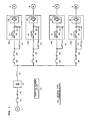
FIG. 1 is a diagram showing the circuit configuration of an example of an electric power converting system according to the invention; -
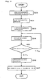
FIG. 2 is a flowchart illustrating the steps of a preliminary operation in removing a failed inverter unit in the electric power converting system shown inFIG. 1 ; -
FIG. 3 is a flowchart illustrating the steps of a preliminary operation in mounting a sound inverter unit after the removal of the failed inverter unit and making the sound inverter unit start an operation in the electric power converting system shown inFIG. 1 ; and -
FIG. 4 is a diagram showing a circuit configuration of an example of a related electric power converting system. -
FIGURE 1 is a diagram showing the circuit configuration of an example of an electric power converting system according to the invention. In the diagram, constituents having the same functions as those of the constituents in the circuit configuration of the related electric power converting system shown inFIG. 4 are denoted with the same reference numerals and signs. - Namely, in an electric
power converting system 60 shown inFIG. 1 , instead of theoperation sequence circuit 11 in the related electric power converting system 10, anoperation sequence circuit 61 is provided. Moreover, disconnectingswitches electromagnetic contactors electromagnetic contactors switches electromagnetic contactors electromagnetic contactors resistors inverter units inverter units capacitors electromagnetic contactors - In the electric
power converting system 60 according to the invention shown inFIG. 1 , in a normal operation, all of amaster disconnecting switch 12, anelectromagnetic contactor 13, thedisconnecting switches electromagnetic contactors electromagnetic contactors - However, when the
capacitors inverter units inverter units inverter units electromagnetic contactors capacitors resistors capacitors electromagnetic contactors resistors power converting system 60 carry out a normal operation. - Suppose that in the electric
power converting system 60 in normal operation, theinverter unit 20a, for example, of theinverter units inverter unit 20a into a state of being stopped. With respect to the operation at this time for replacing the failedinverter unit 20a by an inverter unit capable of carrying out a normal operation will be explained in the following with reference to flow charts shown inFIG. 2 andFIG. 3 . -
FIGURE 2 is a flowchart illustrating the steps of a preliminary operation in removing the failedinverter unit 20a in the electricpower converting system 60 shown inFIG. 1 . - Namely, inFIG.2, in the electric
power converting system 60 made to be in operation by thenormal inverter units switch 25, normally in a closed state, is made opened (step S11) to bring the electricpower converting system 60 into a state in which no output voltage of theconverter 14 is applied to theinverter unit 20a. - In the next, by an instruction from the
operation sequence circuit 61, theelectromagnetic contactor 26 is brought into an opened state (step S12) and, along with this, theelectromagnetic contactors 22 is brought into an opened state (step S13). - Following this, by an instruction from the
operation sequence circuit 61, theelectromagnetic contactor 27, normally being in an opened state, is made closed (step S14), by which the second switching circuit (discharging circuit of the capacitor 23) is formed with the path of the positive potential side of thecapacitor 23 → the charging current suppressingresistor 21 → the contact point of theelectromagnetic contactor 27 → the negative potential side of thecapacitor 23. - Subsequent to this, by an instruction from the
operation sequence circuit 61, a voltage across thecapacitor 23 is measured when the charges remained in thecapacitor 23 are being gradually discharged through the above explained path (step S15). Through the measurement, monitoring is carried out as to whether or not the voltage across thecapacitor 23 is lowered to be equal to or less than the voltage VL previously set as the voltage at which the replacement operation can be safely carried out (step S16). When the monitored voltage exceeds the voltage VL, the operation returns to step S15. Moreover, when the monitored voltage is equal to or less than the voltage VL, it is decided that the voltage across thecapacitor 23 is sufficiently lowered and the operation is shifted to step S17 to inform externally that theinverter unit 20a is in a removable state. - With the steps illustrated by the flow chart explained above, the failed
inverter unit 20a can be safely removed without stopping the electricpower converting system 60 in operation by thenormal inverter units capacitor 23 to discharge with the use of the charging current suppressingresistor 21 which is normally provided in theinverter unit 20a, a discharging time is shortened to make it possible to shorten the time required for the work of replacing the failedinverter unit 20a with a normal one. - In addition, the functions in step S15 and step S16 shown in
FIG. 2 can be replaced by the operation of a timer in which a time, elapsing from the instant when theelectromagnetic contactor 27 is closed in step S14 to the instant when the voltage across thecapacitor 23 lowers to be equal to or less than the voltage VL, is set as a specified standby time. In this case, mounting of a relatively expensive DC voltage detector can be omitted. -
FIGURE 3 is a flowchart illustrating the steps of a preliminary operation in mounting a sound inverter unit after the removal of the failedinverter unit 20a and making the sound inverter unit start an operation in the electricpower converting system 60 shown inFIG. 1 . - Namely, in
FIG. 3 , after thesound inverter unit 20a carrying out a normal operation is mounted, theelectromagnetic contactors operation sequence circuit 61, by which the electricpower converting system 60 is brought into a state in which no output voltage of theconverter 14 is suddenly applied to theinverter unit 20a. - Next, with the disconnecting
switch 25 brought into a closed state (step S22), theelectromagnetic contactor 26 is closed by an instruction from the operation sequence circuit 61 (step S23), by which an output voltage of theconverter 14 is applied to thecapacitor 23 through the charging current suppressingresistor 21. - Then, by an instruction from the
operation sequence circuit 61, the voltage across thecapacitor 23 is measured (step S24) when thecapacitor 23 is gradually charged by the above voltage application operation for monitoring as to whether or not the measured voltage across thecapacitor 23 becomes equal to or more than the previously set minimum permissible input voltage VH (step S25). When the monitored voltage is less than the voltage VH, the operation returns to step S24. Moreover, when the monitored voltage is equal to or more than the voltage VH, it is decided that the voltage across thecapacitor 23 is sufficiently increased and the operation is shifted to step S26 to close theelectromagnetic contactor 22, by which the charging current suppressingresistor 21 is short-circuited to bring theinverter unit 20a into a state in which a normal DC voltage is applied thereto. - Next to this, by an instruction from the
operation sequence circuit 61, a start-up signal is given to theinverter circuit 24 forming theinverter unit 20a (step S27), by which the electricpower converting system 60 is restored to its normal operating condition. - In addition, the functions in step S24 and step S25 shown in
FIG. 3 can be replaced by the operation of a timer in which a time, elapsing from the instant when theelectromagnetic contactor 26 is closed in step S23 to the instant when the voltage across thecapacitor 23 increases to be equal to or more than the voltage VH, is set as a specified standby time. In this case, mounting of a relatively expensive DC voltage detector can be omitted.
While the present invention has been particularly shown and described with reference to the preferred embodiment thereof, it will be understood by those skilled in the art that the foregoing and other changes in form and details can be made therein without departing from the spirit and scope of the present invention.
Claims (3)
- An electric power converting system formed by a plurality of sets of inverters (20a, 30a, 40a, 50a) capable of being operated independently of one another with electric power thereof supplied from a common DC power supply, the electric power system comprising:a plurality of sets of first switching circuits (25, 26; 35, 36; 45, 46; 55,56) provided between the common DC power supply and a plurality of the sets of the inverters as their respective switching circuits; anda plurality of sets of second switching circuits (20a, 30a, 40a, 50a) provided for a plurality of the sets of the inverters as their respective switching circuits for discharging main circuit capacitors (23, 33, 43, 53) respectively forming a plurality of the sets of the inverters.
- The electric power converting system as claimed in claim 1 wherein when at least one of a plurality of the sets of the inverters (20a, 30a, 40a, 50a) is disconnected by the operation of its own first switching circuit (25, 26; 35, 36; 45, 46; 55, 56) from the common DC power supply, the second switching circuit (21, 27; 31, 37; 41, 47; 51, 57), provided for the inverter to be disconnected as its own switching circuit, is made to be operated.
- The electric power converting system as claimed in claim 1 or 2 wherein the main circuit capacitors (23, 33, 43, 53) respectively forming a plurality of the sets of the inverters have their respective charging current suppressing resistors (21, 31, 41, 51) connected thereto and the second switching circuits are operated so as to discharge their respective main circuit capacitors (23, 33, 43, 53) through their respective charging current suppressing resistors (21, 31, 41, 51).
Applications Claiming Priority (1)
| Application Number | Priority Date | Filing Date | Title |
|---|---|---|---|
| JP2010061028A JP5875214B2 (en) | 2010-03-17 | 2010-03-17 | Power conversion system |
Publications (3)
| Publication Number | Publication Date |
|---|---|
| EP2416487A2 true EP2416487A2 (en) | 2012-02-08 |
| EP2416487A3 EP2416487A3 (en) | 2014-10-08 |
| EP2416487B1 EP2416487B1 (en) | 2018-08-15 |
Family
ID=44603026
Family Applications (1)
| Application Number | Title | Priority Date | Filing Date |
|---|---|---|---|
| EP11158460.3A Active EP2416487B1 (en) | 2010-03-17 | 2011-03-16 | Electric power converting system |
Country Status (4)
| Country | Link |
|---|---|
| US (1) | US8896149B2 (en) |
| EP (1) | EP2416487B1 (en) |
| JP (1) | JP5875214B2 (en) |
| CN (1) | CN102195493B (en) |
Families Citing this family (11)
| Publication number | Priority date | Publication date | Assignee | Title |
|---|---|---|---|---|
| EP2644436B1 (en) * | 2012-03-27 | 2018-05-30 | ALSTOM Transport Technologies | Improved hard pre-charge for parallel inverters |
| KR101390641B1 (en) * | 2012-05-07 | 2014-04-30 | 한국에너지기술연구원 | System and method for converting electric power, and apparatus and method for controlling the system |
| CN103580553A (en) * | 2012-07-31 | 2014-02-12 | 施耐德东芝换流器欧洲公司 | Movement and control system |
| US8988841B2 (en) * | 2012-09-06 | 2015-03-24 | Siemens Aktiengesellschaft | Apparatus and methods for input protection for power converters |
| ES2673974T3 (en) * | 2012-11-23 | 2018-06-26 | Moog Unna Gmbh | Conversion system and hydraulic or wind turbine |
| JP2015156740A (en) * | 2014-02-20 | 2015-08-27 | 東芝三菱電機産業システム株式会社 | Power converter |
| WO2015177903A1 (en) * | 2014-05-22 | 2015-11-26 | 三菱電機株式会社 | Inrush current suppression circuit |
| JP6371254B2 (en) * | 2015-05-13 | 2018-08-08 | 東芝三菱電機産業システム株式会社 | Power converter |
| JP2017034801A (en) * | 2015-07-30 | 2017-02-09 | 富士電機株式会社 | Charge control system, power conversion system, charge control device, and power conversion device |
| JP7154907B2 (en) | 2018-09-14 | 2022-10-18 | 株式会社東芝 | semiconductor module |
| JP7396493B2 (en) * | 2021-03-05 | 2023-12-12 | 東芝三菱電機産業システム株式会社 | power converter |
Citations (1)
| Publication number | Priority date | Publication date | Assignee | Title |
|---|---|---|---|---|
| JP2007181331A (en) | 2005-12-28 | 2007-07-12 | Toshiba Mitsubishi-Electric Industrial System Corp | Inverter system |
Family Cites Families (14)
| Publication number | Priority date | Publication date | Assignee | Title |
|---|---|---|---|---|
| US4598263A (en) * | 1984-11-13 | 1986-07-01 | Westinghouse Electric Corp. | Magnetically operated circuit breaker |
| JPH0623195Y2 (en) * | 1985-02-28 | 1994-06-15 | 三菱電機株式会社 | Inverter control circuit |
| JPS62114492A (en) * | 1985-11-11 | 1987-05-26 | Hitachi Ltd | Inverter control device |
| US5170105A (en) | 1991-03-08 | 1992-12-08 | General Electric Company | Method for determining operability of an electrical dynamic braking system |
| JPH06113401A (en) * | 1992-09-28 | 1994-04-22 | Hitachi Ltd | Control device for electric vehicle drive inverter |
| JPH0819266A (en) * | 1994-06-30 | 1996-01-19 | Shimadzu Corp | Inverter device |
| JP3107344B2 (en) | 1994-07-13 | 2000-11-06 | 本田技研工業株式会社 | Control device for electric vehicle motor |
| JPH08275570A (en) * | 1995-01-31 | 1996-10-18 | Mitsubishi Electric Corp | Power control device |
| JP3572915B2 (en) * | 1997-12-16 | 2004-10-06 | 三菱電機株式会社 | A control circuit having an inrush current prevention function, an overvoltage prevention function, and a discharge function, and a power converter including the control circuit |
| JP2000245005A (en) | 1999-02-18 | 2000-09-08 | Toshiba Corp | Vehicle drive control device |
| US8615339B2 (en) * | 2006-04-12 | 2013-12-24 | Mitsubishi Electric Corporation | Control device of electric vehicles |
| JP2008017609A (en) | 2006-07-05 | 2008-01-24 | Toshiba Corp | Electric vehicle control device |
| JP2008017586A (en) | 2006-07-05 | 2008-01-24 | Toyo Electric Mfg Co Ltd | Parallel balance correction control |
| DE102007012590B3 (en) * | 2007-03-13 | 2008-11-27 | Diehl Ako Stiftung & Co. Kg | solar module |
-
2010
- 2010-03-17 JP JP2010061028A patent/JP5875214B2/en active Active
-
2011
- 2011-03-10 US US13/064,196 patent/US8896149B2/en active Active
- 2011-03-16 EP EP11158460.3A patent/EP2416487B1/en active Active
- 2011-03-17 CN CN201110068385.1A patent/CN102195493B/en active Active
Patent Citations (1)
| Publication number | Priority date | Publication date | Assignee | Title |
|---|---|---|---|---|
| JP2007181331A (en) | 2005-12-28 | 2007-07-12 | Toshiba Mitsubishi-Electric Industrial System Corp | Inverter system |
Also Published As
| Publication number | Publication date |
|---|---|
| JP2011199940A (en) | 2011-10-06 |
| CN102195493A (en) | 2011-09-21 |
| JP5875214B2 (en) | 2016-03-02 |
| CN102195493B (en) | 2016-10-05 |
| EP2416487A3 (en) | 2014-10-08 |
| US8896149B2 (en) | 2014-11-25 |
| US20110248564A1 (en) | 2011-10-13 |
| EP2416487B1 (en) | 2018-08-15 |
Similar Documents
| Publication | Publication Date | Title |
|---|---|---|
| US8896149B2 (en) | Electric power converting system | |
| US10044286B2 (en) | Power conversion system including plurality of power converters connected in parallel to load | |
| US10525838B2 (en) | Power conversion system | |
| CN108666966B (en) | Converter with short-circuit fault detection function and short-circuit fault detection method thereof | |
| EP3731368A1 (en) | Power conversion system | |
| US7944089B2 (en) | Uninterruptible power supply module | |
| WO2018113704A1 (en) | A switching arrangement for switching between two inputs, equipment, system and a method | |
| CN1985429A (en) | Frequency converter having an intermediate circuit without any capacitors | |
| CN105406580A (en) | Power supply system and method | |
| CN100382409C (en) | Non-power cutting power supply system | |
| US10940813B2 (en) | Universal platform architecture for hybrid more electric aircraft | |
| CN116349110A (en) | UPS | |
| CN213442110U (en) | Motor drive system and electric automobile | |
| CN100359778C (en) | voltage compensation device | |
| CN210958137U (en) | Bus capacitor discharge circuit and power supply protection system | |
| CN109709479B (en) | Contactor adhesion detection circuit and contactor adhesion detection method | |
| JP2009033943A (en) | Direct high voltage inverter apparatus | |
| JP6584869B2 (en) | Electric vehicle power converter | |
| US12113458B2 (en) | Drive system with common DC bus | |
| CN104753168B (en) | Uninterrupted power supply(ups) | |
| CN214429313U (en) | Power supply switching circuit | |
| WO2020105080A1 (en) | Power conversion device and disconnection detection method | |
| US12132346B2 (en) | UPS module and UPS module control method | |
| JP2014166060A (en) | Power storage device | |
| KR20180096090A (en) | Uninterruptible power supply system |
Legal Events
| Date | Code | Title | Description |
|---|---|---|---|
| AK | Designated contracting states |
Kind code of ref document: A2 Designated state(s): AL AT BE BG CH CY CZ DE DK EE ES FI FR GB GR HR HU IE IS IT LI LT LU LV MC MK MT NL NO PL PT RO RS SE SI SK SM TR |
|
| AX | Request for extension of the european patent |
Extension state: BA ME |
|
| PUAI | Public reference made under article 153(3) epc to a published international application that has entered the european phase |
Free format text: ORIGINAL CODE: 0009012 |
|
| PUAL | Search report despatched |
Free format text: ORIGINAL CODE: 0009013 |
|
| AK | Designated contracting states |
Kind code of ref document: A3 Designated state(s): AL AT BE BG CH CY CZ DE DK EE ES FI FR GB GR HR HU IE IS IT LI LT LU LV MC MK MT NL NO PL PT RO RS SE SI SK SM TR |
|
| AX | Request for extension of the european patent |
Extension state: BA ME |
|
| RIC1 | Information provided on ipc code assigned before grant |
Ipc: H02M 1/00 20070101ALN20140829BHEP Ipc: H02M 1/32 20070101ALN20140829BHEP Ipc: H02M 7/48 20070101AFI20140829BHEP |
|
| 17P | Request for examination filed |
Effective date: 20150408 |
|
| RBV | Designated contracting states (corrected) |
Designated state(s): AL AT BE BG CH CY CZ DE DK EE ES FI FR GB GR HR HU IE IS IT LI LT LU LV MC MK MT NL NO PL PT RO RS SE SI SK SM TR |
|
| STAA | Information on the status of an ep patent application or granted ep patent |
Free format text: STATUS: EXAMINATION IS IN PROGRESS |
|
| 17Q | First examination report despatched |
Effective date: 20170120 |
|
| RIC1 | Information provided on ipc code assigned before grant |
Ipc: H02M 7/48 20070101AFI20171221BHEP Ipc: H02M 1/32 20070101ALN20171221BHEP Ipc: H02M 1/00 20060101ALN20171221BHEP |
|
| GRAP | Despatch of communication of intention to grant a patent |
Free format text: ORIGINAL CODE: EPIDOSNIGR1 |
|
| STAA | Information on the status of an ep patent application or granted ep patent |
Free format text: STATUS: GRANT OF PATENT IS INTENDED |
|
| RIC1 | Information provided on ipc code assigned before grant |
Ipc: H02M 1/00 20060101ALN20180119BHEP Ipc: H02M 7/48 20070101AFI20180119BHEP Ipc: H02M 1/32 20070101ALN20180119BHEP |
|
| INTG | Intention to grant announced |
Effective date: 20180212 |
|
| GRAJ | Information related to disapproval of communication of intention to grant by the applicant or resumption of examination proceedings by the epo deleted |
Free format text: ORIGINAL CODE: EPIDOSDIGR1 |
|
| STAA | Information on the status of an ep patent application or granted ep patent |
Free format text: STATUS: EXAMINATION IS IN PROGRESS |
|
| GRAR | Information related to intention to grant a patent recorded |
Free format text: ORIGINAL CODE: EPIDOSNIGR71 |
|
| GRAS | Grant fee paid |
Free format text: ORIGINAL CODE: EPIDOSNIGR3 |
|
| STAA | Information on the status of an ep patent application or granted ep patent |
Free format text: STATUS: GRANT OF PATENT IS INTENDED |
|
| GRAA | (expected) grant |
Free format text: ORIGINAL CODE: 0009210 |
|
| STAA | Information on the status of an ep patent application or granted ep patent |
Free format text: STATUS: THE PATENT HAS BEEN GRANTED |
|
| INTC | Intention to grant announced (deleted) | ||
| RIC1 | Information provided on ipc code assigned before grant |
Ipc: H02M 7/48 20070101AFI20180625BHEP Ipc: H02M 1/00 20060101ALN20180625BHEP Ipc: H02M 1/32 20070101ALN20180625BHEP |
|
| INTG | Intention to grant announced |
Effective date: 20180704 |
|
| AK | Designated contracting states |
Kind code of ref document: B1 Designated state(s): AL AT BE BG CH CY CZ DE DK EE ES FI FR GB GR HR HU IE IS IT LI LT LU LV MC MK MT NL NO PL PT RO RS SE SI SK SM TR |
|
| REG | Reference to a national code |
Ref country code: CH Ref legal event code: EP Ref country code: GB Ref legal event code: FG4D Ref country code: AT Ref legal event code: REF Ref document number: 1030919 Country of ref document: AT Kind code of ref document: T Effective date: 20180815 |
|
| REG | Reference to a national code |
Ref country code: IE Ref legal event code: FG4D |
|
| REG | Reference to a national code |
Ref country code: DE Ref legal event code: R096 Ref document number: 602011050989 Country of ref document: DE |
|
| REG | Reference to a national code |
Ref country code: NL Ref legal event code: MP Effective date: 20180815 |
|
| REG | Reference to a national code |
Ref country code: LT Ref legal event code: MG4D |
|
| REG | Reference to a national code |
Ref country code: AT Ref legal event code: MK05 Ref document number: 1030919 Country of ref document: AT Kind code of ref document: T Effective date: 20180815 |
|
| PG25 | Lapsed in a contracting state [announced via postgrant information from national office to epo] |
Ref country code: FI Free format text: LAPSE BECAUSE OF FAILURE TO SUBMIT A TRANSLATION OF THE DESCRIPTION OR TO PAY THE FEE WITHIN THE PRESCRIBED TIME-LIMIT Effective date: 20180815 Ref country code: RS Free format text: LAPSE BECAUSE OF FAILURE TO SUBMIT A TRANSLATION OF THE DESCRIPTION OR TO PAY THE FEE WITHIN THE PRESCRIBED TIME-LIMIT Effective date: 20180815 Ref country code: IS Free format text: LAPSE BECAUSE OF FAILURE TO SUBMIT A TRANSLATION OF THE DESCRIPTION OR TO PAY THE FEE WITHIN THE PRESCRIBED TIME-LIMIT Effective date: 20181215 Ref country code: GR Free format text: LAPSE BECAUSE OF FAILURE TO SUBMIT A TRANSLATION OF THE DESCRIPTION OR TO PAY THE FEE WITHIN THE PRESCRIBED TIME-LIMIT Effective date: 20181116 Ref country code: NO Free format text: LAPSE BECAUSE OF FAILURE TO SUBMIT A TRANSLATION OF THE DESCRIPTION OR TO PAY THE FEE WITHIN THE PRESCRIBED TIME-LIMIT Effective date: 20181115 Ref country code: BG Free format text: LAPSE BECAUSE OF FAILURE TO SUBMIT A TRANSLATION OF THE DESCRIPTION OR TO PAY THE FEE WITHIN THE PRESCRIBED TIME-LIMIT Effective date: 20181115 Ref country code: AT Free format text: LAPSE BECAUSE OF FAILURE TO SUBMIT A TRANSLATION OF THE DESCRIPTION OR TO PAY THE FEE WITHIN THE PRESCRIBED TIME-LIMIT Effective date: 20180815 Ref country code: NL Free format text: LAPSE BECAUSE OF FAILURE TO SUBMIT A TRANSLATION OF THE DESCRIPTION OR TO PAY THE FEE WITHIN THE PRESCRIBED TIME-LIMIT Effective date: 20180815 Ref country code: SE Free format text: LAPSE BECAUSE OF FAILURE TO SUBMIT A TRANSLATION OF THE DESCRIPTION OR TO PAY THE FEE WITHIN THE PRESCRIBED TIME-LIMIT Effective date: 20180815 Ref country code: LT Free format text: LAPSE BECAUSE OF FAILURE TO SUBMIT A TRANSLATION OF THE DESCRIPTION OR TO PAY THE FEE WITHIN THE PRESCRIBED TIME-LIMIT Effective date: 20180815 |
|
| PG25 | Lapsed in a contracting state [announced via postgrant information from national office to epo] |
Ref country code: AL Free format text: LAPSE BECAUSE OF FAILURE TO SUBMIT A TRANSLATION OF THE DESCRIPTION OR TO PAY THE FEE WITHIN THE PRESCRIBED TIME-LIMIT Effective date: 20180815 Ref country code: ES Free format text: LAPSE BECAUSE OF FAILURE TO SUBMIT A TRANSLATION OF THE DESCRIPTION OR TO PAY THE FEE WITHIN THE PRESCRIBED TIME-LIMIT Effective date: 20180815 Ref country code: LV Free format text: LAPSE BECAUSE OF FAILURE TO SUBMIT A TRANSLATION OF THE DESCRIPTION OR TO PAY THE FEE WITHIN THE PRESCRIBED TIME-LIMIT Effective date: 20180815 Ref country code: HR Free format text: LAPSE BECAUSE OF FAILURE TO SUBMIT A TRANSLATION OF THE DESCRIPTION OR TO PAY THE FEE WITHIN THE PRESCRIBED TIME-LIMIT Effective date: 20180815 |
|
| PG25 | Lapsed in a contracting state [announced via postgrant information from national office to epo] |
Ref country code: PL Free format text: LAPSE BECAUSE OF FAILURE TO SUBMIT A TRANSLATION OF THE DESCRIPTION OR TO PAY THE FEE WITHIN THE PRESCRIBED TIME-LIMIT Effective date: 20180815 Ref country code: RO Free format text: LAPSE BECAUSE OF FAILURE TO SUBMIT A TRANSLATION OF THE DESCRIPTION OR TO PAY THE FEE WITHIN THE PRESCRIBED TIME-LIMIT Effective date: 20180815 Ref country code: CZ Free format text: LAPSE BECAUSE OF FAILURE TO SUBMIT A TRANSLATION OF THE DESCRIPTION OR TO PAY THE FEE WITHIN THE PRESCRIBED TIME-LIMIT Effective date: 20180815 Ref country code: IT Free format text: LAPSE BECAUSE OF FAILURE TO SUBMIT A TRANSLATION OF THE DESCRIPTION OR TO PAY THE FEE WITHIN THE PRESCRIBED TIME-LIMIT Effective date: 20180815 Ref country code: EE Free format text: LAPSE BECAUSE OF FAILURE TO SUBMIT A TRANSLATION OF THE DESCRIPTION OR TO PAY THE FEE WITHIN THE PRESCRIBED TIME-LIMIT Effective date: 20180815 |
|
| REG | Reference to a national code |
Ref country code: DE Ref legal event code: R097 Ref document number: 602011050989 Country of ref document: DE |
|
| PG25 | Lapsed in a contracting state [announced via postgrant information from national office to epo] |
Ref country code: DK Free format text: LAPSE BECAUSE OF FAILURE TO SUBMIT A TRANSLATION OF THE DESCRIPTION OR TO PAY THE FEE WITHIN THE PRESCRIBED TIME-LIMIT Effective date: 20180815 Ref country code: SM Free format text: LAPSE BECAUSE OF FAILURE TO SUBMIT A TRANSLATION OF THE DESCRIPTION OR TO PAY THE FEE WITHIN THE PRESCRIBED TIME-LIMIT Effective date: 20180815 Ref country code: SK Free format text: LAPSE BECAUSE OF FAILURE TO SUBMIT A TRANSLATION OF THE DESCRIPTION OR TO PAY THE FEE WITHIN THE PRESCRIBED TIME-LIMIT Effective date: 20180815 |
|
| PLBE | No opposition filed within time limit |
Free format text: ORIGINAL CODE: 0009261 |
|
| STAA | Information on the status of an ep patent application or granted ep patent |
Free format text: STATUS: NO OPPOSITION FILED WITHIN TIME LIMIT |
|
| 26N | No opposition filed |
Effective date: 20190516 |
|
| PG25 | Lapsed in a contracting state [announced via postgrant information from national office to epo] |
Ref country code: SI Free format text: LAPSE BECAUSE OF FAILURE TO SUBMIT A TRANSLATION OF THE DESCRIPTION OR TO PAY THE FEE WITHIN THE PRESCRIBED TIME-LIMIT Effective date: 20180815 |
|
| PG25 | Lapsed in a contracting state [announced via postgrant information from national office to epo] |
Ref country code: MC Free format text: LAPSE BECAUSE OF FAILURE TO SUBMIT A TRANSLATION OF THE DESCRIPTION OR TO PAY THE FEE WITHIN THE PRESCRIBED TIME-LIMIT Effective date: 20180815 |
|
| REG | Reference to a national code |
Ref country code: CH Ref legal event code: PL |
|
| GBPC | Gb: european patent ceased through non-payment of renewal fee |
Effective date: 20190316 |
|
| PG25 | Lapsed in a contracting state [announced via postgrant information from national office to epo] |
Ref country code: LU Free format text: LAPSE BECAUSE OF NON-PAYMENT OF DUE FEES Effective date: 20190316 |
|
| REG | Reference to a national code |
Ref country code: BE Ref legal event code: MM Effective date: 20190331 |
|
| PG25 | Lapsed in a contracting state [announced via postgrant information from national office to epo] |
Ref country code: IE Free format text: LAPSE BECAUSE OF NON-PAYMENT OF DUE FEES Effective date: 20190316 Ref country code: LI Free format text: LAPSE BECAUSE OF NON-PAYMENT OF DUE FEES Effective date: 20190331 Ref country code: CH Free format text: LAPSE BECAUSE OF NON-PAYMENT OF DUE FEES Effective date: 20190331 Ref country code: GB Free format text: LAPSE BECAUSE OF NON-PAYMENT OF DUE FEES Effective date: 20190316 |
|
| PG25 | Lapsed in a contracting state [announced via postgrant information from national office to epo] |
Ref country code: FR Free format text: LAPSE BECAUSE OF NON-PAYMENT OF DUE FEES Effective date: 20190331 Ref country code: BE Free format text: LAPSE BECAUSE OF NON-PAYMENT OF DUE FEES Effective date: 20190331 |
|
| PG25 | Lapsed in a contracting state [announced via postgrant information from national office to epo] |
Ref country code: TR Free format text: LAPSE BECAUSE OF FAILURE TO SUBMIT A TRANSLATION OF THE DESCRIPTION OR TO PAY THE FEE WITHIN THE PRESCRIBED TIME-LIMIT Effective date: 20180815 |
|
| PG25 | Lapsed in a contracting state [announced via postgrant information from national office to epo] |
Ref country code: PT Free format text: LAPSE BECAUSE OF FAILURE TO SUBMIT A TRANSLATION OF THE DESCRIPTION OR TO PAY THE FEE WITHIN THE PRESCRIBED TIME-LIMIT Effective date: 20181215 Ref country code: MT Free format text: LAPSE BECAUSE OF NON-PAYMENT OF DUE FEES Effective date: 20190316 |
|
| PG25 | Lapsed in a contracting state [announced via postgrant information from national office to epo] |
Ref country code: CY Free format text: LAPSE BECAUSE OF FAILURE TO SUBMIT A TRANSLATION OF THE DESCRIPTION OR TO PAY THE FEE WITHIN THE PRESCRIBED TIME-LIMIT Effective date: 20180815 |
|
| PG25 | Lapsed in a contracting state [announced via postgrant information from national office to epo] |
Ref country code: HU Free format text: LAPSE BECAUSE OF FAILURE TO SUBMIT A TRANSLATION OF THE DESCRIPTION OR TO PAY THE FEE WITHIN THE PRESCRIBED TIME-LIMIT; INVALID AB INITIO Effective date: 20110316 |
|
| PG25 | Lapsed in a contracting state [announced via postgrant information from national office to epo] |
Ref country code: MK Free format text: LAPSE BECAUSE OF FAILURE TO SUBMIT A TRANSLATION OF THE DESCRIPTION OR TO PAY THE FEE WITHIN THE PRESCRIBED TIME-LIMIT Effective date: 20180815 |
|
| PGFP | Annual fee paid to national office [announced via postgrant information from national office to epo] |
Ref country code: DE Payment date: 20260128 Year of fee payment: 16 |