EP2416363A1 - Organic electroluminescent device - Google Patents
Organic electroluminescent device Download PDFInfo
- Publication number
- EP2416363A1 EP2416363A1 EP11176411A EP11176411A EP2416363A1 EP 2416363 A1 EP2416363 A1 EP 2416363A1 EP 11176411 A EP11176411 A EP 11176411A EP 11176411 A EP11176411 A EP 11176411A EP 2416363 A1 EP2416363 A1 EP 2416363A1
- Authority
- EP
- European Patent Office
- Prior art keywords
- color filter
- substrate
- organic electroluminescent
- filter pattern
- electrode
- Prior art date
- Legal status (The legal status is an assumption and is not a legal conclusion. Google has not performed a legal analysis and makes no representation as to the accuracy of the status listed.)
- Granted
Links
Images


Classifications
-
- H—ELECTRICITY
- H10—SEMICONDUCTOR DEVICES; ELECTRIC SOLID-STATE DEVICES NOT OTHERWISE PROVIDED FOR
- H10K—ORGANIC ELECTRIC SOLID-STATE DEVICES
- H10K59/00—Integrated devices, or assemblies of multiple devices, comprising at least one organic light-emitting element covered by group H10K50/00
- H10K59/30—Devices specially adapted for multicolour light emission
- H10K59/38—Devices specially adapted for multicolour light emission comprising colour filters or colour changing media [CCM]
-
- H—ELECTRICITY
- H10—SEMICONDUCTOR DEVICES; ELECTRIC SOLID-STATE DEVICES NOT OTHERWISE PROVIDED FOR
- H10K—ORGANIC ELECTRIC SOLID-STATE DEVICES
- H10K50/00—Organic light-emitting devices
-
- H—ELECTRICITY
- H10—SEMICONDUCTOR DEVICES; ELECTRIC SOLID-STATE DEVICES NOT OTHERWISE PROVIDED FOR
- H10K—ORGANIC ELECTRIC SOLID-STATE DEVICES
- H10K59/00—Integrated devices, or assemblies of multiple devices, comprising at least one organic light-emitting element covered by group H10K50/00
- H10K59/30—Devices specially adapted for multicolour light emission
- H10K59/35—Devices specially adapted for multicolour light emission comprising red-green-blue [RGB] subpixels
- H10K59/351—Devices specially adapted for multicolour light emission comprising red-green-blue [RGB] subpixels comprising more than three subpixels, e.g. red-green-blue-white [RGBW]
Definitions
- the present invention relates to an organic electroluminescent device (OELD), more particularly, to an OELD having reduced consumption power and improved ambient contrast ratio.
- OELD organic electroluminescent device
- An OELD of new flat panel display devices is a self-emitting type.
- the OELD has excellent characteristics of a view angel, a contrast ratio and so on. Also, since the OELD does not require a backlight assembly, the OELD has low weight and low power consumption. Moreover, the OELD has advantages of a high response rate, a low production cost and so on.
- the OELD may be classified into a passive matrix type and an active matrix type.
- anodes are arranged perpendicular to cathodes. The intersection of the cathode and anode make up the pixel where light is emitted. External circuitry applies current to selected strips of anode and cathode such that one pixel is turned on and other pixels are turned off. The brightness of each pixel is proportional to the amount of applied current.
- the passive matrix type OELD is easy to make, but more power is required.
- a thin film transistor (TFT) as a switching element is positioned in each pixel.
- a first electrode, which is connected to the TFT, is turned on and off in each pixel, and a second electrode facing the first electrode serves as a common electrode.
- an applied voltage is charged in a storage capacitor, the voltage is maintained by next frame. Accordingly, the active matrix type OELD requires a lower power, so it is efficient for large display devices.
- FIG. 1 is a circuit diagram showing a pixel region of the related art OELD.
- a gate line “GL”, a data line “DL”, a power supply line “PL”, a switching thin film transistor (TFT) "STr”, a storage capacitor “StgC”, a driving TFT “DTr”, and an organic electroluminescent diode “E” are formed in one pixel region “P".
- the gate line “GL” and the data line “DL” cross each other such that the pixel region "P" is defined, and the power supply line “PL” is formed to be parallel to the data line "DL”.
- the switching TFT “STr” is formed at crossing portion of the gate and data line “GL” and “DL”.
- the driving TFT “DTr” is electrically connected to the switching TFT "STr”.
- the driving TFT "DTr” is electrically connected to the organic electroluminescent diode "E".
- a first electrode of the organic electroluminescent diode “E” is connected to a drain electrode of the driving TFT "DTr”
- a second electrode of the organic electroluminescent diode “E” is connected to the power supply line "PL”.
- the power supply line "PL” provides a source voltage to the organic electroluminescent diode "E”.
- the storage capacitor “Cst” is disposed between gate and source electrodes of the driving TFT "Tr”.
- the storage capacitor "StgC” serves as maintaining the voltage of the gate electrode of the driving TFT “DTr” when the switching TFT "STr” is turned off. Accordingly, even if the switching TFT "STr” is turned off, a level of an electric current applied from the power supply line "PL" to the organic electroluminescent diode "E” is maintained to next frame.
- An organic emitting layer of the OELD may include organic emitting materials for emitting red, green and blue colors.
- the organic emitting layer may include an organic emitting material for emitting a white light, and red, green and blue color filter patterns are formed in each pixel.
- an OELD displaying a color image using a white pixel with red, green and blue pixels is introduced.
- a circular polarizer is positioned at outmost side of the display device.
- the circular polarizer causes an increase of power consumption.
- the color filter patterns are used for increasing the ambient contrast ratio.
- the OELD including a white organic emitting layer uses color filters to display a color image.
- the OELD is intended to increase the ambient contrast ratio without the circular polarizer.
- the OELD including the red, green and blue color filter patterns without the white pixel has an advantage in the ambient contrast ratio but has a disadvantage in power consumption.
- a color coordinate of a device displaying a white light is equal to a reference color coordinate of a panel.
- the reference color coordinate becomes less by driving the blue pixel, which has less transmittance.
- the blue pixel is also driven with the white pixel, power consumption is increased.
- the present invention is directed to an OELD that substantially obviates one or more of the problems due to limitations and disadvantages of the related art.
- an organic electroluminescent device includes a first substrate including first to fourth pixel regions; an organic electroluminescent diode on the first substrate and in each of the first to fourth pixel regions, the organic electroluminescent diode emitting a white light; a second substrate facing the first substrate; and a color filter layer positioned between the organic electroluminescent diode and the second substrate or between the organic electroluminescent diode and the first substrate and including a red color filter pattern, a green color filter pattern, a blue color filter pattern and a white color filter pattern corresponding to the first to fourth pixel regions, respectively, wherein the white color filter pattern has a first transmittance with respect to a blue light greater than a second transmittance with respect to a red light and a green light.
- FIG. 1 is a circuit diagram showing a pixel region of the related art OELD.
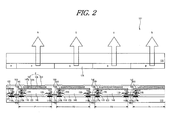
- FIG. 2 is a schematic cross-sectional view showing red, green, blue and white pixel regions of an OELD according to the present invention.
- FIG. 3 is a graph showing power consumption in OELDs.
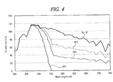
- FIG. 4 is a graph showing an external light reflection in OELDs.
- FIG. 2 is a schematic cross-sectional view showing red, green, blue and white pixel regions of an OELD according to the present invention.
- a switching region where a switching thin film transistor (TFT) is formed
- a driving region where a driving TFT is formed
- an OELD 101 includes a first substrate 110, a switching TFT (not shown), a driving TFT DTr, an organic electroluminescent diode E, a second substrate 170, which faces the first substrate 110, and a color filter layer 175.
- the switching TFT (not shown), the driving TFT DTr and the organic electroluminescent diode E are positioned on the first substrate 110, and the color filter layer 175 is positioned on the second substrate 170.
- the color filter layer 175 includes a red color filter pattern R, a green color filter pattern G, a blue color filter pattern B and a white color filter pattern W.
- a first semiconductor layer 113 including a first region 113a as a channel and second regions 113b at both sides of the first region 113a are formed in the driving region DA.
- the first region 113a is formed of intrinsic polycrystalline silicon, and high impurities are doped in the second regions 113b.
- a buffer layer which is formed of an inorganic insulating material, such as silicon oxide and silicon nitride, may be formed between the first substrate 110 and the first semiconductor layer 113. Due to the buffer layer, property degradation of the semiconductor layer 113 by alkali ions from the first substrate 110 during a crystallization process of the semiconductor layer 113 is prevented.
- a second semiconductor layer including a third region as a channel and fourth regions at both sides of the third region is formed in the switching region.
- a gate insulating layer 116 is formed on the first semiconductor layer 113 and the second semiconductor layer, and a first gate electrode 120 is formed on the gate insulating layer 116.
- the first gate electrode 120 corresponding to the first region 113a of the first semiconductor layer 113. Namely, the first gate electrode 120 overlaps the first region 113a.
- a second gate electrode corresponding to the third region of the second semiconductor layer is formed on the gate insulating layer 116.
- a gate line (not shown) connected to the second gate electrode is also formed on the gate insulating layer 116.
- An interlayer insulating layer 123 is formed on the first gate electrode 120, the second gate electrode and the gate line.
- the interlayer insulating layer 123 and the gate insulating layer 116 are patterned to form first semiconductor contact holes 125 respectively exposing the second regions 113b of the first semiconductor layer 113.
- second semiconductor contact holes respectively exposing the fourth regions of the second semiconductor layer are formed thorough the interlayer insulating layer 123 and the gate insulating layer 116.
- a first source electrode 133 and a first drain electrode 136 are formed on the interlayer insulating layer 123.
- the first source electrode 133 and the first drain electrode 136 respectively contact the second regions 113b through the first semiconductor contact holes 125.
- a second source electrode and a second drain electrode are formed on the interlayer insulating layer 123.
- the second source electrode and the second drain electrode respectively contact the fourth regions through the second semiconductor contact holes.
- a data line and a power line are formed on the interlayer insulating layer 123.
- the data line crosses the gate line to define first to fourth pixel regions P1, P2, P3 and P4.
- the data line is connected to the second source electrode in the switching region, and the power line is connected to the first source electrode in the driving region.
- the first semiconductor layer 113, the first gate electrode 120, the first source electrode 133 and the first drain electrode 136 constitute the driving TFT DTr.
- the second semiconductor layer, the second gate electrode, the second source electrode and the second drain electrode constitute the switching TFT.
- the switching TFT is electrically connected to the driving TFT DTr, the gate line and the data line.
- the switching TFT and the driving TFT DTr are classified into a p-type or an n-type TFT depending on a doped impurity.
- a trivalent atom such as boron is doped into the second regions 113b to form the p-type TFT.
- a hole is used as a carrier.
- a first electrode 147 of the organic electroluminescent diode E serves as an anode or a cathode depending on a type of the driving TFT DTr.
- the driving TFT DTr is the p-type such that the first electrode 147 serves as the anode.
- FIG. 2 shows the driving TFT DTr being as a top gate type and including the semiconductor layer of polycrystalline silicon.
- each of the driving TFT DTr and the switching TFT may be a bottom gate type and include the semiconductor layers of amorphous silicon.
- the gate electrode, the gate insulating layer, the semiconductor layer including an active layer of intrinsic amorphous silicon and an ohmic contact layer of impurity-doped silicon are sequentially stacked, and the source electrode and the drain electrode are positioned on the semiconductor layer.
- the gate line is positioned at the same layer as the gate electrode, and the data line is positioned at the same layer as the source electrode.
- the gate line is connected to the gate electrode of the switching TFT, and the data line is connected to the source electrode of the switching TFT.
- a passivation layer 140 is formed on the switching TFT and the driving TFT DTr.
- the passivation layer 140 has a drain contact hole 143 exposing the first drain electrode 136 of the driving TFT DTr.
- the first electrode 147 is formed in each of the first to fourth pixel regions P1, P2, P3 and P4.
- the first electrode 147 contacts the first drain electrode 136 of the driving TFT DTr through the drain contact hole 143.
- the first electrode 147 has a double-layered structure.
- a lower layer 147a serves as a reflection plate, and an upper layer 147b serves as an anode.
- the upper layer 147b is formed of a transparent conductive material such as indium-tin-oxide (ITO) and indium-zinc-oxide (IZO). Since the transparent conductive material has a relatively high work function such that the upper layer 147b serves as the anode.
- the lower layer 147a is formed of a relative high reflection efficiency material such as aluminum (A1) and silver (Ag) to reflect light toward the second substrate 170.
- a buffer pattern 150 corresponding to edges of the first electrode 147 is formed. Namely, the buffer pattern 150 surrounds each of the first to fourth pixel regions P1, P2, P3 and P4.
- the buffer pattern 150 may be formed of an organic insulating material such as polyimide, photo-acryl and benzocyclobutene (BCB).
- the buffer pattern 150 may be formed of a black resin.
- an organic emitting layer 155 is formed on the first electrode 147.
- the organic emitting layer 155 emits white light and is surrounded by the buffer pattern 150.
- a second electrode 158 covering an entire display area of the first substrate 110 is formed on the organic emitting layer 155.
- the first electrode 147, the organic emitting layer 155 and the second electrode 158 constitute the organic electroluminescent diode E.
- a first emission-compensation layer and a second emission-compensation layer may be formed between the first electrode 147 and the organic emitting layer 155 and between the second electrode 158 and the organic emitting layer 155, respectively.
- the first emission-compensation layer includes a hole injection layer and a hole transporting layer
- the second emission-compensation layer includes an electron transporting layer and an electron injection layer.
- Each of the first and second emission-compensation layers may cover an entire display area of the first substrate or may be positioned in each of the first to fourth pixel regions P1, P2, P3 and P4.
- the second electrode 158 is formed of a relatively low work function material such as Al, Al alloy, Ag, magnesium (Mg), gold (Au) and Al-Mg alloy (AlMg) to serve as a cathode.
- the second electrode 158 has a thickness of about 10 to 200 angstroms such that light from the organic emitting layer 155 passes through the second electrode 158.
- the first electrode 147 and the second electrode 158 respectively serve as the anode and the cathode.
- the first electrode 147 may be formed of a relatively low work function material to serve as a cathode
- the second electrode 158 may be formed of a relatively high work function material to serve as an anode.
- the color filter layer 175 includes the red color filter pattern R as a first color filter pattern, the green color filter pattern G as a second color filter pattern and the blue color filter pattern B as a fourth color filter pattern corresponding to the first to third pixel regions P1, P2 and P3, respectively.
- the color filter layer 175 further includes a white color filter pattern W as a fourth color filter pattern corresponding to the fourth pixel region P4.
- the white color filter pattern W emits bluish-white light.
- an overcoat layer may be formed on the color filter layer 175.
- a white color filter pattern is formed of a transparent resin having substantially the same transmittance of 30 to 35% with respect to the red light, the green light and the blue light.
- the white color filter pattern W has a blue light transmittance greater than each of a red light transmittance and a green light transmittance.
- the white color filter pattern W is formed of a transparent resin having a first transmittance of about 50 to 99% to a wavelength of 450 to 550 nm, i.e., a blue light, and a second transmittance of about 10 to 90% to a wavelength of 550 to 780 nm, i.e., a red light or a green light.
- the white color filter pattern W Since the white color filter pattern W has the first transmittance to the blue light being greater than the second transmittance to the red light and/or the green light, the white color filter pattern W emits the bluish-white light. Due to the white color filter pattern W, which emits the bluish-white light, in the fourth pixel region P4, the ambient contrast ratio is increase.
- an efficiency of a white device is maximized when an efficiency of each of red, green and blue devices is maximized.
- an efficiency of the blue device is smaller than that of the red and green devices, there is a limitation in increasing a color temperature of the white device, e.g., 5000 to 8000 K.
- the red, green and blue pixel regions should be driven with the white pixel region.
- the white pixel region has an emitting efficiency greater than the red, green and blue pixel regions, power consumption of the panel can be reduced when the color temperature of the white pixel region is adjusted to the reference color temperature of the panel.
- the white color filter pattern W which emits the bluish-white light and provides a desired color temperature
- power consumption of the OELD is reduced.
- an ambient contrast ratio is improved.
- the ambient contrast ratio is controlled by the white color filter pattern W, there is the degree of the freedom in the ambient contrast ratio.
- the white color filter pattern W includes a dye of a weight % of about 0.1 to 15.
- the dye is a blue color dye or a mixture of the blue color dye and a purple color dye.
- FIG. 3 is a graph showing power consumption in OELDs.
- "CF1" is a graph in an OELD including a white color filter pattern only transmitting a blue light
- CF4 is a graph in an OELD including a white color filter pattern in the present invention
- "CF5" is a graph in an OELD including a white color filter pattern having substantially the same transmittance with respect to the red, green and blue lights
- "No CF” is a graph in an OELD without a white color filter pattern.
- FIG. 3 shows power consumption of the panel when an image having a color temperature of 9000 K and a brightness of about 200 nit.
- the OELD "CF4" in the present invention having the white color filter pattern, which has a blue light transmittance greater than each of a red light transmittance and a green light transmittance, has the power consumption of about 5.9 W.
- the OELD "No CF" without the white color filter pattern has the power consumption of about 7.74 W
- an the OELD "CF5" has the power consumption of about 6.72 W.
- the OELD "CF1" has the power consumption of about 15.45 W. Namely, the OELD according to the present invention has an advantage in power consumption with the same condition.
- FIG. 4 is a graph showing an external light reflection in OELDs.
- the external light reflection has smallest intensity in the OELD "CF1" and largest intensity in the OELD "No CF”.
- the OELD "CF4" in the present invention has larger external light reflection intensity than the OELD "CF1” and smaller external light reflection intensity than the OELD "No CF” and the OELD "CF5".
- the external light reflection intensity of the OELD "CF4" in the present invention is about half of that of the OELD "No CF”. Namely, the external light reflection is relatively decreased in the OELD of the present invention such that the ambient contrast ratio is relatively increased.
- the OELD in the present invention has advantages in the power consumption and the ambient contrast ratio with compared to other OELDs.
- a seal pattern or a frit pattern (not shown) as a bonding element is formed along an edge of the first substrate 110 or the second substrate 170 such that the first and second substrates 110 and 170 are attached to each other under a condition of vacuum or an inert gas.
- a circular polarizer may be further formed on an outer side of the second substrate 170 to further improve the ambient contrast ratio. Even though the power consumption is increased with the circular, the power consumption in the OELD of the present invention is still lower than other OELDs because the power consumption is lowest as shown in FIG. 3 .
- the buffer pattern 150 may be formed of a transparent organic material.
- the buffer pattern 150 may be formed of a black resin for the ambient contrast ratio.
- FIG. 2 shows a top emission type OELD where the color filter layer 175 is formed between the organic electroluminescent diode E and the second substrate 170.
- the color filter layer 175 may be formed between the first substrate and the organic electroluminescent diode E to obtain a bottom emission type OELD.
- the circular polarizer is positioned on an outer side of the first substrate such that the color filter layer 175 is positioned between the circular polarizer and the organic electroluminescent diode "E".
Landscapes
- Physics & Mathematics (AREA)
- Optics & Photonics (AREA)
- Electroluminescent Light Sources (AREA)
Abstract
Description
- The present application claims the benefit of Korean Patent Application Nos.
10-2010-0075112 10-2010-0079404 - The present invention relates to an organic electroluminescent device (OELD), more particularly, to an OELD having reduced consumption power and improved ambient contrast ratio.
- An OELD of new flat panel display devices is a self-emitting type. The OELD has excellent characteristics of a view angel, a contrast ratio and so on. Also, since the OELD does not require a backlight assembly, the OELD has low weight and low power consumption. Moreover, the OELD has advantages of a high response rate, a low production cost and so on.
- The OELD may be classified into a passive matrix type and an active matrix type.
- In the passive matrix type OELD, anodes are arranged perpendicular to cathodes. The intersection of the cathode and anode make up the pixel where light is emitted. External circuitry applies current to selected strips of anode and cathode such that one pixel is turned on and other pixels are turned off. The brightness of each pixel is proportional to the amount of applied current. The passive matrix type OELD is easy to make, but more power is required.
- In the active matrix type OELD, a thin film transistor (TFT) as a switching element is positioned in each pixel. A first electrode, which is connected to the TFT, is turned on and off in each pixel, and a second electrode facing the first electrode serves as a common electrode. In addition, an applied voltage is charged in a storage capacitor, the voltage is maintained by next frame. Accordingly, the active matrix type OELD requires a lower power, so it is efficient for large display devices.
-
FIG. 1 is a circuit diagram showing a pixel region of the related art OELD. As shown inFIG. 1 , a gate line "GL", a data line "DL", a power supply line "PL", a switching thin film transistor (TFT) "STr", a storage capacitor "StgC", a driving TFT "DTr", and an organic electroluminescent diode "E" are formed in one pixel region "P". The gate line "GL" and the data line "DL" cross each other such that the pixel region "P" is defined, and the power supply line "PL" is formed to be parallel to the data line "DL". The switching TFT "STr" is formed at crossing portion of the gate and data line "GL" and "DL". The driving TFT "DTr" is electrically connected to the switching TFT "STr". - The driving TFT "DTr" is electrically connected to the organic electroluminescent diode "E". In more detail, a first electrode of the organic electroluminescent diode "E" is connected to a drain electrode of the driving TFT "DTr", and a second electrode of the organic electroluminescent diode "E" is connected to the power supply line "PL". The power supply line "PL" provides a source voltage to the organic electroluminescent diode "E". The storage capacitor "Cst" is disposed between gate and source electrodes of the driving TFT "Tr".
- When a signal is applied to the switching TFT "STr" through the gate line "GL" such that the switching TFT "STr" is turned on, a signal from the data line "DL" is applied to the gate electrode of the driving TFT "DTr" such that the driving TFT "DTr" is turned on. As a result, light is emitted from the organic electroluminescent diode "E". In this case, when the driving TFT "DTr" is turned on, a level of an electric current applied from the power supply line "PL" to the organic electroluminescent diode "E" is determined such that the organic electroluminescent diode "E" can produce a gray scale. The storage capacitor "StgC" serves as maintaining the voltage of the gate electrode of the driving TFT "DTr" when the switching TFT "STr" is turned off. Accordingly, even if the switching TFT "STr" is turned off, a level of an electric current applied from the power supply line "PL" to the organic electroluminescent diode "E" is maintained to next frame.
- An organic emitting layer of the OELD may include organic emitting materials for emitting red, green and blue colors. Alternatively, the organic emitting layer may include an organic emitting material for emitting a white light, and red, green and blue color filter patterns are formed in each pixel.
- Recently, to increase brightness and reduce power consumption, an OELD displaying a color image using a white pixel with red, green and blue pixels is introduced.
- On the other hand, to improve an ambient contrast ration (ACR) of the display device, a circular polarizer is positioned at outmost side of the display device. Unfortunately, the circular polarizer causes an increase of power consumption.
- To prevent the increase of power consumption, the color filter patterns are used for increasing the ambient contrast ratio. However, there is a limitation in increasing the ambient contrast ratio because there is no color filter pattern in the white pixel. In more detail, the OELD including a white organic emitting layer uses color filters to display a color image. In the OELD is intended to increase the ambient contrast ratio without the circular polarizer. However, since there is no color filter pattern in the white pixel, there is bad effect on the ambient contrast ratio. On the other hand, the OELD including the red, green and blue color filter patterns without the white pixel has an advantage in the ambient contrast ratio but has a disadvantage in power consumption.
- Generally, in the OELD including red, green, blue and white pixels, power consumption is reduced when a color coordinate of a device displaying a white light is equal to a reference color coordinate of a panel. In general, since a color coordinate of a device displaying a white light is less than a reference color coordinate of a panel, the reference color coordinate becomes less by driving the blue pixel, which has less transmittance. In this case, since the blue pixel is also driven with the white pixel, power consumption is increased.
- Accordingly, the present invention is directed to an OELD that substantially obviates one or more of the problems due to limitations and disadvantages of the related art.
- Additional features and advantages of the invention will be set forth in the description which follows, and in part will be apparent from the description, or may be learned by practice of the invention. These and other advantages of the invention will be realized and attained by the structure particularly pointed out in the written description and claims hereof as well as the appended drawings.
- In accordance with the present invention, as embodied and broadly described herein, an organic electroluminescent device includes a first substrate including first to fourth pixel regions; an organic electroluminescent diode on the first substrate and in each of the first to fourth pixel regions, the organic electroluminescent diode emitting a white light; a second substrate facing the first substrate; and a color filter layer positioned between the organic electroluminescent diode and the second substrate or between the organic electroluminescent diode and the first substrate and including a red color filter pattern, a green color filter pattern, a blue color filter pattern and a white color filter pattern corresponding to the first to fourth pixel regions, respectively, wherein the white color filter pattern has a first transmittance with respect to a blue light greater than a second transmittance with respect to a red light and a green light.
- It is to be understood that both the foregoing general description and the following detailed description are exemplary and explanatory and are intended to provide further explanation of the invention as claimed.
- The accompanying drawings, which are included to provide a further understanding of the invention and are incorporated in and constitute a part of this specification, illustrate embodiments of the invention and together with the description serve to explain the principles of the invention.
-
FIG. 1 is a circuit diagram showing a pixel region of the related art OELD. -
FIG. 2 is a schematic cross-sectional view showing red, green, blue and white pixel regions of an OELD according to the present invention. -
FIG. 3 is a graph showing power consumption in OELDs. -
FIG. 4 is a graph showing an external light reflection in OELDs. - Reference will now be made in detail to the preferred embodiments, examples of which are illustrated in the accompanying drawings.
-
FIG. 2 is a schematic cross-sectional view showing red, green, blue and white pixel regions of an OELD according to the present invention. For convenience of explanation, a switching region, where a switching thin film transistor (TFT) is formed, and a driving region, where a driving TFT is formed, are defined. - As shown in
FIG. 2 , an OELD 101 according to the present invention includes afirst substrate 110, a switching TFT (not shown), a driving TFT DTr, an organic electroluminescent diode E, asecond substrate 170, which faces thefirst substrate 110, and acolor filter layer 175. The switching TFT (not shown), the driving TFT DTr and the organic electroluminescent diode E are positioned on thefirst substrate 110, and thecolor filter layer 175 is positioned on thesecond substrate 170. Thecolor filter layer 175 includes a red color filter pattern R, a green color filter pattern G, a blue color filter pattern B and a white color filter pattern W. - On the
first substrate 110, a first semiconductor layer 113 including afirst region 113a as a channel andsecond regions 113b at both sides of thefirst region 113a are formed in the driving region DA. Thefirst region 113a is formed of intrinsic polycrystalline silicon, and high impurities are doped in thesecond regions 113b. Although not shown, a buffer layer, which is formed of an inorganic insulating material, such as silicon oxide and silicon nitride, may be formed between thefirst substrate 110 and the first semiconductor layer 113. Due to the buffer layer, property degradation of the semiconductor layer 113 by alkali ions from thefirst substrate 110 during a crystallization process of the semiconductor layer 113 is prevented. - Although not shown, a second semiconductor layer including a third region as a channel and fourth regions at both sides of the third region is formed in the switching region.
- A
gate insulating layer 116 is formed on the first semiconductor layer 113 and the second semiconductor layer, and afirst gate electrode 120 is formed on thegate insulating layer 116. Thefirst gate electrode 120 corresponding to thefirst region 113a of the first semiconductor layer 113. Namely, thefirst gate electrode 120 overlaps thefirst region 113a. Although not shown, a second gate electrode corresponding to the third region of the second semiconductor layer is formed on thegate insulating layer 116. - A gate line (not shown) connected to the second gate electrode is also formed on the
gate insulating layer 116. - An interlayer insulating
layer 123 is formed on thefirst gate electrode 120, the second gate electrode and the gate line. The interlayer insulatinglayer 123 and thegate insulating layer 116 are patterned to form first semiconductor contact holes 125 respectively exposing thesecond regions 113b of the first semiconductor layer 113. Although not shown, second semiconductor contact holes respectively exposing the fourth regions of the second semiconductor layer are formed thorough the interlayer insulatinglayer 123 and thegate insulating layer 116. - On the
interlayer insulating layer 123, afirst source electrode 133 and afirst drain electrode 136 are formed. Thefirst source electrode 133 and thefirst drain electrode 136 respectively contact thesecond regions 113b through the first semiconductor contact holes 125. Although not shown, a second source electrode and a second drain electrode are formed on theinterlayer insulating layer 123. The second source electrode and the second drain electrode respectively contact the fourth regions through the second semiconductor contact holes. In addition, a data line and a power line are formed on theinterlayer insulating layer 123. The data line crosses the gate line to define first to fourth pixel regions P1, P2, P3 and P4. The data line is connected to the second source electrode in the switching region, and the power line is connected to the first source electrode in the driving region. - The first semiconductor layer 113, the
first gate electrode 120, thefirst source electrode 133 and thefirst drain electrode 136 constitute the driving TFT DTr. In addition, the second semiconductor layer, the second gate electrode, the second source electrode and the second drain electrode constitute the switching TFT. The switching TFT is electrically connected to the driving TFT DTr, the gate line and the data line. - The switching TFT and the driving TFT DTr are classified into a p-type or an n-type TFT depending on a doped impurity. For example, a trivalent atom such as boron is doped into the
second regions 113b to form the p-type TFT. In the p-type TFT, a hole is used as a carrier. - On the other hand, a
first electrode 147 of the organic electroluminescent diode E serves as an anode or a cathode depending on a type of the driving TFT DTr. In the present invention, the driving TFT DTr is the p-type such that thefirst electrode 147 serves as the anode. -
FIG. 2 shows the driving TFT DTr being as a top gate type and including the semiconductor layer of polycrystalline silicon. Alternatively, each of the driving TFT DTr and the switching TFT may be a bottom gate type and include the semiconductor layers of amorphous silicon. In the bottom gate type TFTs, the gate electrode, the gate insulating layer, the semiconductor layer including an active layer of intrinsic amorphous silicon and an ohmic contact layer of impurity-doped silicon are sequentially stacked, and the source electrode and the drain electrode are positioned on the semiconductor layer. The gate line is positioned at the same layer as the gate electrode, and the data line is positioned at the same layer as the source electrode. The gate line is connected to the gate electrode of the switching TFT, and the data line is connected to the source electrode of the switching TFT. - On the switching TFT and the driving TFT DTr, a
passivation layer 140 is formed. Thepassivation layer 140 has adrain contact hole 143 exposing thefirst drain electrode 136 of the driving TFT DTr. - On the
passivation layer 140, thefirst electrode 147 is formed in each of the first to fourth pixel regions P1, P2, P3 and P4. Thefirst electrode 147 contacts thefirst drain electrode 136 of the driving TFT DTr through thedrain contact hole 143. In the present invention, thefirst electrode 147 has a double-layered structure. Alower layer 147a serves as a reflection plate, and anupper layer 147b serves as an anode. Theupper layer 147b is formed of a transparent conductive material such as indium-tin-oxide (ITO) and indium-zinc-oxide (IZO). Since the transparent conductive material has a relatively high work function such that theupper layer 147b serves as the anode. Thelower layer 147a is formed of a relative high reflection efficiency material such as aluminum (A1) and silver (Ag) to reflect light toward thesecond substrate 170. - A
buffer pattern 150 corresponding to edges of thefirst electrode 147 is formed. Namely, thebuffer pattern 150 surrounds each of the first to fourth pixel regions P1, P2, P3 and P4. For example, thebuffer pattern 150 may be formed of an organic insulating material such as polyimide, photo-acryl and benzocyclobutene (BCB). Alternatively, thebuffer pattern 150 may be formed of a black resin. - In each of the first to fourth pixel regions P1, P2, P3 and P4, an organic emitting
layer 155 is formed on thefirst electrode 147. The organic emittinglayer 155 emits white light and is surrounded by thebuffer pattern 150. In addition, asecond electrode 158 covering an entire display area of thefirst substrate 110 is formed on the organic emittinglayer 155. Thefirst electrode 147, the organic emittinglayer 155 and thesecond electrode 158 constitute the organic electroluminescent diode E. - Although not shown, to increase an emitting efficiency of the organic emitting
layer 155, a first emission-compensation layer and a second emission-compensation layer may be formed between thefirst electrode 147 and the organic emittinglayer 155 and between thesecond electrode 158 and the organic emittinglayer 155, respectively. The first emission-compensation layer includes a hole injection layer and a hole transporting layer, and the second emission-compensation layer includes an electron transporting layer and an electron injection layer. Each of the first and second emission-compensation layers may cover an entire display area of the first substrate or may be positioned in each of the first to fourth pixel regions P1, P2, P3 and P4. - The
second electrode 158 is formed of a relatively low work function material such as Al, Al alloy, Ag, magnesium (Mg), gold (Au) and Al-Mg alloy (AlMg) to serve as a cathode. Thesecond electrode 158 has a thickness of about 10 to 200 angstroms such that light from the organic emittinglayer 155 passes through thesecond electrode 158. - As mentioned above, the
first electrode 147 and thesecond electrode 158 respectively serve as the anode and the cathode. Alternatively, thefirst electrode 147 may be formed of a relatively low work function material to serve as a cathode, and thesecond electrode 158 may be formed of a relatively high work function material to serve as an anode. - On the
second substrate 170, thecolor filter layer 175 is formed. Thecolor filter layer 175 includes the red color filter pattern R as a first color filter pattern, the green color filter pattern G as a second color filter pattern and the blue color filter pattern B as a fourth color filter pattern corresponding to the first to third pixel regions P1, P2 and P3, respectively. In addition, thecolor filter layer 175 further includes a white color filter pattern W as a fourth color filter pattern corresponding to the fourth pixel region P4. The white color filter pattern W emits bluish-white light. Although not shown, an overcoat layer may be formed on thecolor filter layer 175. - Generally, a white color filter pattern is formed of a transparent resin having substantially the same transmittance of 30 to 35% with respect to the red light, the green light and the blue light.
- However, in the
OELD 101 according to the present invention, the white color filter pattern W has a blue light transmittance greater than each of a red light transmittance and a green light transmittance. Namely, the white color filter pattern W is formed of a transparent resin having a first transmittance of about 50 to 99% to a wavelength of 450 to 550 nm, i.e., a blue light, and a second transmittance of about 10 to 90% to a wavelength of 550 to 780 nm, i.e., a red light or a green light. Since the white color filter pattern W has the first transmittance to the blue light being greater than the second transmittance to the red light and/or the green light, the white color filter pattern W emits the bluish-white light. Due to the white color filter pattern W, which emits the bluish-white light, in the fourth pixel region P4, the ambient contrast ratio is increase. - Generally, an efficiency of a white device is maximized when an efficiency of each of red, green and blue devices is maximized. However, since an efficiency of the blue device is smaller than that of the red and green devices, there is a limitation in increasing a color temperature of the white device, e.g., 5000 to 8000 K. In addition, in order that the white device meets a color temperature above 9000K, which is required in the general display device, the red, green and blue pixel regions should be driven with the white pixel region.
- On the other hand, since the white pixel region has an emitting efficiency greater than the red, green and blue pixel regions, power consumption of the panel can be reduced when the color temperature of the white pixel region is adjusted to the reference color temperature of the panel.
- In the present invention, by forming the white color filter pattern W, which emits the bluish-white light and provides a desired color temperature, in the fourth pixel region P4, power consumption of the OELD is reduced. In addition, by reducing an ambient light reflection in the fourth pixel region P4, an ambient contrast ratio is improved. Moreover, since the ambient contrast ratio is controlled by the white color filter pattern W, there is the degree of the freedom in the ambient contrast ratio.
- The white color filter pattern W includes a dye of a weight % of about 0.1 to 15. The dye is a blue color dye or a mixture of the blue color dye and a purple color dye.
-
FIG. 3 is a graph showing power consumption in OELDs. InFIG. 3 , "CF1" is a graph in an OELD including a white color filter pattern only transmitting a blue light, and "CF4" is a graph in an OELD including a white color filter pattern in the present invention. "CF5" is a graph in an OELD including a white color filter pattern having substantially the same transmittance with respect to the red, green and blue lights, and "No CF" is a graph in an OELD without a white color filter pattern.FIG. 3 shows power consumption of the panel when an image having a color temperature of 9000 K and a brightness of about 200 nit. - As shown in
FIG. 3 , the OELD "CF4" in the present invention having the white color filter pattern, which has a blue light transmittance greater than each of a red light transmittance and a green light transmittance, has the power consumption of about 5.9 W. On the other hand, the OELD "No CF" without the white color filter pattern has the power consumption of about 7.74 W, an the OELD "CF5" has the power consumption of about 6.72 W. The OELD "CF1" has the power consumption of about 15.45 W. Namely, the OELD according to the present invention has an advantage in power consumption with the same condition. -
FIG. 4 is a graph showing an external light reflection in OELDs. As shown inFIG. 4 , the external light reflection has smallest intensity in the OELD "CF1" and largest intensity in the OELD "No CF". The OELD "CF4" in the present invention has larger external light reflection intensity than the OELD "CF1" and smaller external light reflection intensity than the OELD "No CF" and the OELD "CF5". The external light reflection intensity of the OELD "CF4" in the present invention is about half of that of the OELD "No CF". Namely, the external light reflection is relatively decreased in the OELD of the present invention such that the ambient contrast ratio is relatively increased. - Referring to
FIGs. 3 and4 , the OELD in the present invention has advantages in the power consumption and the ambient contrast ratio with compared to other OELDs. - Referring back to
FIG. 2 , a seal pattern or a frit pattern (not shown) as a bonding element is formed along an edge of thefirst substrate 110 or thesecond substrate 170 such that the first andsecond substrates - Although not shown, a circular polarizer may be further formed on an outer side of the
second substrate 170 to further improve the ambient contrast ratio. Even though the power consumption is increased with the circular, the power consumption in the OELD of the present invention is still lower than other OELDs because the power consumption is lowest as shown inFIG. 3 . With the circular polarizer, thebuffer pattern 150 may be formed of a transparent organic material. On the other hand, without the circular polarizer, thebuffer pattern 150 may be formed of a black resin for the ambient contrast ratio. -
FIG. 2 shows a top emission type OELD where thecolor filter layer 175 is formed between the organic electroluminescent diode E and thesecond substrate 170. Alternatively, thecolor filter layer 175 may be formed between the first substrate and the organic electroluminescent diode E to obtain a bottom emission type OELD. In this case, the circular polarizer is positioned on an outer side of the first substrate such that thecolor filter layer 175 is positioned between the circular polarizer and the organic electroluminescent diode "E". - It will be apparent to those skilled in the art that various modifications and variations can be made in the present invention without departing from the spirit or scope of the invention. Thus, it is intended that the present invention cover the modifications and variations of this invention provided they come within the scope of the appended claims and their equivalents.
Claims (9)
- An organic electroluminescent device, comprising:a first substrate including first to fourth pixel regions;an organic electroluminescent diode on the first substrate and in each of the first to fourth pixel regions, the organic electroluminescent diode emitting a white light;a second substrate facing the first substrate; anda color filter layer positioned between the organic electroluminescent diode and the second substrate or between the organic electroluminescent diode and the first substrate and including a red color filter pattern, a green color filter pattern, a blue color filter pattern and a white color filter pattern corresponding to the first to fourth pixel regions, respectively,wherein the white color filter pattern has a first transmittance with respect to a blue light greater than a second transmittance with respect to a red light and a green light.
- The device according to claim 1, wherein the first transmittance has a range of about 50 to 99 %, and the second transmittance has a range of about 10 to 90 %.
- The device according to claim 1, further comprising:a switching thin film transistor in each of the first to fourth pixel regions;a driving thin film transistor in each of the first to fourth pixel regions and connected to the switching thin film transistora gate line and a data line crossing each other and electrically connected to the switching thin film transistor; anda power line electrically connected to the driving thin film transistor.
- The device according to claim 3, wherein the organic electroluminescent diode includes a first electrode, a second electrode and an organic emitting layer between the first and second electrodes, and the first electrode is connected to the driving thin film transistor.
- The device according to claim 4, wherein further comprising a buffer pattern surrounding the organic emitting layer.
- The device according to claim 5, wherein the buffer pattern is formed of a transparent organic insulating material or a black resin.
- The device according to claim 1, further comprising a circular polarizer between on an outer side of the first substrate or the second substrate such that the color filter layer is positioned between the circular polarizer and the organic electroluminescent diode.
- The device according to claim 1, wherein the white color filter layer includes a dye having a weight % of about 0.1 to 15.
- The device according to claim 8, wherein the dye is a blue color dye or a mixture of the blue color dye and a purple color dye.
Applications Claiming Priority (2)
| Application Number | Priority Date | Filing Date | Title |
|---|---|---|---|
| KR20100075112 | 2010-08-03 | ||
| KR1020100079404A KR101241131B1 (en) | 2010-08-03 | 2010-08-17 | Organic electro luminescent device |
Publications (2)
| Publication Number | Publication Date |
|---|---|
| EP2416363A1 true EP2416363A1 (en) | 2012-02-08 |
| EP2416363B1 EP2416363B1 (en) | 2020-04-22 |
Family
ID=44925698
Family Applications (1)
| Application Number | Title | Priority Date | Filing Date |
|---|---|---|---|
| EP11176411.4A Active EP2416363B1 (en) | 2010-08-03 | 2011-08-03 | Organic electroluminescent device |
Country Status (4)
| Country | Link |
|---|---|
| US (1) | US8421345B2 (en) |
| EP (1) | EP2416363B1 (en) |
| KR (1) | KR101241131B1 (en) |
| CN (1) | CN102347348B (en) |
Cited By (1)
| Publication number | Priority date | Publication date | Assignee | Title |
|---|---|---|---|---|
| GB2567551A (en) * | 2017-08-31 | 2019-04-17 | Lg Display Co Ltd | Organic light emitting display device |
Families Citing this family (19)
| Publication number | Priority date | Publication date | Assignee | Title |
|---|---|---|---|---|
| KR20140113923A (en) * | 2012-01-16 | 2014-09-25 | 소니 주식회사 | Solid-state image sensor and camera system |
| KR20130142715A (en) * | 2012-06-20 | 2013-12-30 | 삼성디스플레이 주식회사 | Polarization structure, method of manufacturing a polarization structure and display device including a polarization structure |
| KR101931173B1 (en) * | 2012-07-27 | 2018-12-21 | 삼성디스플레이 주식회사 | Organic light emitting display device |
| JP2015037062A (en) * | 2013-08-15 | 2015-02-23 | ソニー株式会社 | Display device and electronic apparatus |
| JP6578641B2 (en) * | 2014-06-19 | 2019-09-25 | 大日本印刷株式会社 | Color filter for organic electroluminescence display device and organic electroluminescence display device |
| KR102284214B1 (en) * | 2014-09-23 | 2021-08-02 | 삼성디스플레이 주식회사 | Display device comprising gray color filter |
| KR20160035680A (en) | 2014-09-23 | 2016-04-01 | 삼성디스플레이 주식회사 | Display device comprising gray color filter |
| KR20160079975A (en) * | 2014-12-26 | 2016-07-07 | 삼성디스플레이 주식회사 | Organec light emitting display device and method of manufacturing the same |
| KR20160084553A (en) * | 2015-01-05 | 2016-07-14 | 삼성디스플레이 주식회사 | LIQUID CRYSTAL DISPLAY DEVICE having white pixel |
| KR20160087047A (en) * | 2015-01-12 | 2016-07-21 | 삼성디스플레이 주식회사 | Display device |
| KR102431372B1 (en) * | 2015-07-20 | 2022-08-11 | 엘지디스플레이 주식회사 | Color Filter Array Substrate And Organic Light Emitting Diode Display Device Including The Same |
| KR20170133564A (en) | 2016-05-25 | 2017-12-06 | 삼성디스플레이 주식회사 | Organic light emitting display |
| CN106125185B (en) * | 2016-08-29 | 2019-02-26 | 武汉华星光电技术有限公司 | Display screen and its polaroid |
| CN106125179B (en) * | 2016-08-29 | 2019-02-26 | 武汉华星光电技术有限公司 | Display device and filter thereof |
| KR102437327B1 (en) * | 2017-12-27 | 2022-08-29 | 엘지디스플레이 주식회사 | Display device |
| WO2019215538A1 (en) | 2018-05-11 | 2019-11-14 | 株式会社半導体エネルギー研究所 | Display device, display module, and electronic device |
| KR102885546B1 (en) * | 2019-07-25 | 2025-11-12 | 엘지디스플레이 주식회사 | Organic Light Emitting Diode Display Device |
| KR102785979B1 (en) * | 2020-01-21 | 2025-03-27 | 삼성디스플레이 주식회사 | Display panel |
| KR20230091225A (en) | 2021-12-15 | 2023-06-23 | 삼성디스플레이 주식회사 | Display device |
Citations (5)
| Publication number | Priority date | Publication date | Assignee | Title |
|---|---|---|---|---|
| US20050218768A1 (en) * | 2004-03-30 | 2005-10-06 | Sanyo Electric Co., Ltd. | Organic electroluminescent apparatus |
| US20090072693A1 (en) * | 2007-09-17 | 2009-03-19 | Cok Ronald S | Led device having improved light output |
| KR20100075112A (en) | 2008-12-24 | 2010-07-02 | 삼성테크윈 주식회사 | Waste tape removal device |
| US20100171910A1 (en) * | 2009-01-08 | 2010-07-08 | Yun-I Liu | Display Device and Display Panel and Color Filter thereof |
| KR20100079404A (en) | 2008-12-31 | 2010-07-08 | 주식회사 메이텍 | Transfer system for picker portion of test handler |
Family Cites Families (7)
| Publication number | Priority date | Publication date | Assignee | Title |
|---|---|---|---|---|
| JP4011292B2 (en) * | 2001-01-15 | 2007-11-21 | 株式会社日立製作所 | LIGHT EMITTING ELEMENT AND DISPLAY DEVICE |
| US20050147844A1 (en) * | 2004-01-05 | 2005-07-07 | Eastman Kodak Company | White oled devices with color filter arrays |
| JP2007019014A (en) * | 2005-07-06 | 2007-01-25 | Samsung Sdi Co Ltd | Flat panel display device and manufacturing method thereof |
| EP2654034B1 (en) * | 2006-06-19 | 2016-09-07 | Sharp Kabushiki Kaisha | Display device |
| JP4899929B2 (en) * | 2007-02-28 | 2012-03-21 | セイコーエプソン株式会社 | Display device |
| JP5007602B2 (en) | 2007-05-09 | 2012-08-22 | セイコーエプソン株式会社 | Electroluminescence device and electronic device |
| KR20090104765A (en) * | 2008-03-31 | 2009-10-06 | 스미또모 가가꾸 가부시키가이샤 | Color filter |
-
2010
- 2010-08-17 KR KR1020100079404A patent/KR101241131B1/en active Active
-
2011
- 2011-07-27 US US13/192,316 patent/US8421345B2/en active Active
- 2011-08-03 CN CN201110225412.1A patent/CN102347348B/en active Active
- 2011-08-03 EP EP11176411.4A patent/EP2416363B1/en active Active
Patent Citations (5)
| Publication number | Priority date | Publication date | Assignee | Title |
|---|---|---|---|---|
| US20050218768A1 (en) * | 2004-03-30 | 2005-10-06 | Sanyo Electric Co., Ltd. | Organic electroluminescent apparatus |
| US20090072693A1 (en) * | 2007-09-17 | 2009-03-19 | Cok Ronald S | Led device having improved light output |
| KR20100075112A (en) | 2008-12-24 | 2010-07-02 | 삼성테크윈 주식회사 | Waste tape removal device |
| KR20100079404A (en) | 2008-12-31 | 2010-07-08 | 주식회사 메이텍 | Transfer system for picker portion of test handler |
| US20100171910A1 (en) * | 2009-01-08 | 2010-07-08 | Yun-I Liu | Display Device and Display Panel and Color Filter thereof |
Cited By (3)
| Publication number | Priority date | Publication date | Assignee | Title |
|---|---|---|---|---|
| GB2567551A (en) * | 2017-08-31 | 2019-04-17 | Lg Display Co Ltd | Organic light emitting display device |
| US10516002B2 (en) | 2017-08-31 | 2019-12-24 | Lg Display Co., Ltd. | Organic light emitting display device |
| GB2567551B (en) * | 2017-08-31 | 2021-03-10 | Lg Display Co Ltd | Organic light emitting display device including light absorption material layer |
Also Published As
| Publication number | Publication date |
|---|---|
| KR20120012940A (en) | 2012-02-13 |
| EP2416363B1 (en) | 2020-04-22 |
| CN102347348A (en) | 2012-02-08 |
| KR101241131B1 (en) | 2013-03-11 |
| CN102347348B (en) | 2015-11-25 |
| US20120032583A1 (en) | 2012-02-09 |
| US8421345B2 (en) | 2013-04-16 |
Similar Documents
| Publication | Publication Date | Title |
|---|---|---|
| EP2416363B1 (en) | Organic electroluminescent device | |
| JP3995476B2 (en) | Display device and manufacturing method thereof | |
| KR101589272B1 (en) | Touch sensor in-cell type organic electroluminescent device and methode of fabricating the same | |
| US7482746B2 (en) | Liquid crystal display apparatus having reflective layer | |
| KR101697611B1 (en) | Organic electro luminescent device | |
| US10396133B2 (en) | Two-way organic light emitting diode display device | |
| KR20170012664A (en) | Thin Film Transistor Array Substrate And Organic Light Emitting Diode Display Device Including The Same | |
| US9590022B2 (en) | Dual emitting device for active matrix organic electroluminescence | |
| US12324341B2 (en) | Transparent display device for reducing difference in visibility between display area and bezel area | |
| US12349548B2 (en) | Display device | |
| KR102564169B1 (en) | Organic light emitting diodes, Head mounted display including the same, and method for manufacturing the same. | |
| US20250372042A1 (en) | Display with dyed interlayer to reduce external reflectance | |
| KR101770592B1 (en) | Organic electro-luminescent Device | |
| JP2007140547A (en) | Display device and its manufacturing method | |
| US20250275445A1 (en) | Display device | |
| US20260059986A1 (en) | Light emitting display device | |
| KR102888573B1 (en) | Electroluminescent display device | |
| US20240224661A1 (en) | Dual-side organic light emitting display device | |
| CN120021398A (en) | Display device | |
| JP2005215646A (en) | Electro-optical device and electronic apparatus | |
| KR20250119044A (en) | Display apparatus | |
| KR20100065687A (en) | Dual plate type organic electro-luminescent device and the method for fabricating thereof |
Legal Events
| Date | Code | Title | Description |
|---|---|---|---|
| AK | Designated contracting states |
Kind code of ref document: A1 Designated state(s): AL AT BE BG CH CY CZ DE DK EE ES FI FR GB GR HR HU IE IS IT LI LT LU LV MC MK MT NL NO PL PT RO RS SE SI SK SM TR |
|
| AX | Request for extension of the european patent |
Extension state: BA ME |
|
| PUAI | Public reference made under article 153(3) epc to a published international application that has entered the european phase |
Free format text: ORIGINAL CODE: 0009012 |
|
| 17P | Request for examination filed |
Effective date: 20120313 |
|
| STAA | Information on the status of an ep patent application or granted ep patent |
Free format text: STATUS: EXAMINATION IS IN PROGRESS |
|
| 17Q | First examination report despatched |
Effective date: 20170717 |
|
| GRAP | Despatch of communication of intention to grant a patent |
Free format text: ORIGINAL CODE: EPIDOSNIGR1 |
|
| STAA | Information on the status of an ep patent application or granted ep patent |
Free format text: STATUS: GRANT OF PATENT IS INTENDED |
|
| INTG | Intention to grant announced |
Effective date: 20200123 |
|
| GRAS | Grant fee paid |
Free format text: ORIGINAL CODE: EPIDOSNIGR3 |
|
| GRAA | (expected) grant |
Free format text: ORIGINAL CODE: 0009210 |
|
| STAA | Information on the status of an ep patent application or granted ep patent |
Free format text: STATUS: THE PATENT HAS BEEN GRANTED |
|
| AK | Designated contracting states |
Kind code of ref document: B1 Designated state(s): AL AT BE BG CH CY CZ DE DK EE ES FI FR GB GR HR HU IE IS IT LI LT LU LV MC MK MT NL NO PL PT RO RS SE SI SK SM TR |
|
| REG | Reference to a national code |
Ref country code: GB Ref legal event code: FG4D |
|
| REG | Reference to a national code |
Ref country code: CH Ref legal event code: EP |
|
| REG | Reference to a national code |
Ref country code: IE Ref legal event code: FG4D |
|
| REG | Reference to a national code |
Ref country code: DE Ref legal event code: R096 Ref document number: 602011066358 Country of ref document: DE |
|
| REG | Reference to a national code |
Ref country code: AT Ref legal event code: REF Ref document number: 1261278 Country of ref document: AT Kind code of ref document: T Effective date: 20200515 |
|
| REG | Reference to a national code |
Ref country code: LT Ref legal event code: MG4D |
|
| REG | Reference to a national code |
Ref country code: NL Ref legal event code: MP Effective date: 20200422 |
|
| PG25 | Lapsed in a contracting state [announced via postgrant information from national office to epo] |
Ref country code: SE Free format text: LAPSE BECAUSE OF FAILURE TO SUBMIT A TRANSLATION OF THE DESCRIPTION OR TO PAY THE FEE WITHIN THE PRESCRIBED TIME-LIMIT Effective date: 20200422 Ref country code: IS Free format text: LAPSE BECAUSE OF FAILURE TO SUBMIT A TRANSLATION OF THE DESCRIPTION OR TO PAY THE FEE WITHIN THE PRESCRIBED TIME-LIMIT Effective date: 20200822 Ref country code: FI Free format text: LAPSE BECAUSE OF FAILURE TO SUBMIT A TRANSLATION OF THE DESCRIPTION OR TO PAY THE FEE WITHIN THE PRESCRIBED TIME-LIMIT Effective date: 20200422 Ref country code: PT Free format text: LAPSE BECAUSE OF FAILURE TO SUBMIT A TRANSLATION OF THE DESCRIPTION OR TO PAY THE FEE WITHIN THE PRESCRIBED TIME-LIMIT Effective date: 20200824 Ref country code: GR Free format text: LAPSE BECAUSE OF FAILURE TO SUBMIT A TRANSLATION OF THE DESCRIPTION OR TO PAY THE FEE WITHIN THE PRESCRIBED TIME-LIMIT Effective date: 20200723 Ref country code: NO Free format text: LAPSE BECAUSE OF FAILURE TO SUBMIT A TRANSLATION OF THE DESCRIPTION OR TO PAY THE FEE WITHIN THE PRESCRIBED TIME-LIMIT Effective date: 20200722 Ref country code: NL Free format text: LAPSE BECAUSE OF FAILURE TO SUBMIT A TRANSLATION OF THE DESCRIPTION OR TO PAY THE FEE WITHIN THE PRESCRIBED TIME-LIMIT Effective date: 20200422 Ref country code: LT Free format text: LAPSE BECAUSE OF FAILURE TO SUBMIT A TRANSLATION OF THE DESCRIPTION OR TO PAY THE FEE WITHIN THE PRESCRIBED TIME-LIMIT Effective date: 20200422 |
|
| REG | Reference to a national code |
Ref country code: AT Ref legal event code: MK05 Ref document number: 1261278 Country of ref document: AT Kind code of ref document: T Effective date: 20200422 |
|
| PG25 | Lapsed in a contracting state [announced via postgrant information from national office to epo] |
Ref country code: RS Free format text: LAPSE BECAUSE OF FAILURE TO SUBMIT A TRANSLATION OF THE DESCRIPTION OR TO PAY THE FEE WITHIN THE PRESCRIBED TIME-LIMIT Effective date: 20200422 Ref country code: BG Free format text: LAPSE BECAUSE OF FAILURE TO SUBMIT A TRANSLATION OF THE DESCRIPTION OR TO PAY THE FEE WITHIN THE PRESCRIBED TIME-LIMIT Effective date: 20200722 Ref country code: HR Free format text: LAPSE BECAUSE OF FAILURE TO SUBMIT A TRANSLATION OF THE DESCRIPTION OR TO PAY THE FEE WITHIN THE PRESCRIBED TIME-LIMIT Effective date: 20200422 Ref country code: LV Free format text: LAPSE BECAUSE OF FAILURE TO SUBMIT A TRANSLATION OF THE DESCRIPTION OR TO PAY THE FEE WITHIN THE PRESCRIBED TIME-LIMIT Effective date: 20200422 |
|
| PG25 | Lapsed in a contracting state [announced via postgrant information from national office to epo] |
Ref country code: AL Free format text: LAPSE BECAUSE OF FAILURE TO SUBMIT A TRANSLATION OF THE DESCRIPTION OR TO PAY THE FEE WITHIN THE PRESCRIBED TIME-LIMIT Effective date: 20200422 |
|
| REG | Reference to a national code |
Ref country code: DE Ref legal event code: R097 Ref document number: 602011066358 Country of ref document: DE |
|
| PG25 | Lapsed in a contracting state [announced via postgrant information from national office to epo] |
Ref country code: SM Free format text: LAPSE BECAUSE OF FAILURE TO SUBMIT A TRANSLATION OF THE DESCRIPTION OR TO PAY THE FEE WITHIN THE PRESCRIBED TIME-LIMIT Effective date: 20200422 Ref country code: RO Free format text: LAPSE BECAUSE OF FAILURE TO SUBMIT A TRANSLATION OF THE DESCRIPTION OR TO PAY THE FEE WITHIN THE PRESCRIBED TIME-LIMIT Effective date: 20200422 Ref country code: IT Free format text: LAPSE BECAUSE OF FAILURE TO SUBMIT A TRANSLATION OF THE DESCRIPTION OR TO PAY THE FEE WITHIN THE PRESCRIBED TIME-LIMIT Effective date: 20200422 Ref country code: AT Free format text: LAPSE BECAUSE OF FAILURE TO SUBMIT A TRANSLATION OF THE DESCRIPTION OR TO PAY THE FEE WITHIN THE PRESCRIBED TIME-LIMIT Effective date: 20200422 Ref country code: DK Free format text: LAPSE BECAUSE OF FAILURE TO SUBMIT A TRANSLATION OF THE DESCRIPTION OR TO PAY THE FEE WITHIN THE PRESCRIBED TIME-LIMIT Effective date: 20200422 Ref country code: EE Free format text: LAPSE BECAUSE OF FAILURE TO SUBMIT A TRANSLATION OF THE DESCRIPTION OR TO PAY THE FEE WITHIN THE PRESCRIBED TIME-LIMIT Effective date: 20200422 Ref country code: ES Free format text: LAPSE BECAUSE OF FAILURE TO SUBMIT A TRANSLATION OF THE DESCRIPTION OR TO PAY THE FEE WITHIN THE PRESCRIBED TIME-LIMIT Effective date: 20200422 Ref country code: CZ Free format text: LAPSE BECAUSE OF FAILURE TO SUBMIT A TRANSLATION OF THE DESCRIPTION OR TO PAY THE FEE WITHIN THE PRESCRIBED TIME-LIMIT Effective date: 20200422 |
|
| PG25 | Lapsed in a contracting state [announced via postgrant information from national office to epo] |
Ref country code: PL Free format text: LAPSE BECAUSE OF FAILURE TO SUBMIT A TRANSLATION OF THE DESCRIPTION OR TO PAY THE FEE WITHIN THE PRESCRIBED TIME-LIMIT Effective date: 20200422 Ref country code: SK Free format text: LAPSE BECAUSE OF FAILURE TO SUBMIT A TRANSLATION OF THE DESCRIPTION OR TO PAY THE FEE WITHIN THE PRESCRIBED TIME-LIMIT Effective date: 20200422 |
|
| PLBE | No opposition filed within time limit |
Free format text: ORIGINAL CODE: 0009261 |
|
| STAA | Information on the status of an ep patent application or granted ep patent |
Free format text: STATUS: NO OPPOSITION FILED WITHIN TIME LIMIT |
|
| 26N | No opposition filed |
Effective date: 20210125 |
|
| PG25 | Lapsed in a contracting state [announced via postgrant information from national office to epo] |
Ref country code: MC Free format text: LAPSE BECAUSE OF FAILURE TO SUBMIT A TRANSLATION OF THE DESCRIPTION OR TO PAY THE FEE WITHIN THE PRESCRIBED TIME-LIMIT Effective date: 20200422 |
|
| REG | Reference to a national code |
Ref country code: CH Ref legal event code: PL |
|
| PG25 | Lapsed in a contracting state [announced via postgrant information from national office to epo] |
Ref country code: CH Free format text: LAPSE BECAUSE OF NON-PAYMENT OF DUE FEES Effective date: 20200831 Ref country code: LI Free format text: LAPSE BECAUSE OF NON-PAYMENT OF DUE FEES Effective date: 20200831 Ref country code: LU Free format text: LAPSE BECAUSE OF NON-PAYMENT OF DUE FEES Effective date: 20200803 |
|
| REG | Reference to a national code |
Ref country code: BE Ref legal event code: MM Effective date: 20200831 |
|
| PG25 | Lapsed in a contracting state [announced via postgrant information from national office to epo] |
Ref country code: SI Free format text: LAPSE BECAUSE OF FAILURE TO SUBMIT A TRANSLATION OF THE DESCRIPTION OR TO PAY THE FEE WITHIN THE PRESCRIBED TIME-LIMIT Effective date: 20200422 |
|
| PG25 | Lapsed in a contracting state [announced via postgrant information from national office to epo] |
Ref country code: BE Free format text: LAPSE BECAUSE OF NON-PAYMENT OF DUE FEES Effective date: 20200831 Ref country code: IE Free format text: LAPSE BECAUSE OF NON-PAYMENT OF DUE FEES Effective date: 20200803 |
|
| PG25 | Lapsed in a contracting state [announced via postgrant information from national office to epo] |
Ref country code: TR Free format text: LAPSE BECAUSE OF FAILURE TO SUBMIT A TRANSLATION OF THE DESCRIPTION OR TO PAY THE FEE WITHIN THE PRESCRIBED TIME-LIMIT Effective date: 20200422 Ref country code: MT Free format text: LAPSE BECAUSE OF FAILURE TO SUBMIT A TRANSLATION OF THE DESCRIPTION OR TO PAY THE FEE WITHIN THE PRESCRIBED TIME-LIMIT Effective date: 20200422 Ref country code: CY Free format text: LAPSE BECAUSE OF FAILURE TO SUBMIT A TRANSLATION OF THE DESCRIPTION OR TO PAY THE FEE WITHIN THE PRESCRIBED TIME-LIMIT Effective date: 20200422 |
|
| PG25 | Lapsed in a contracting state [announced via postgrant information from national office to epo] |
Ref country code: MK Free format text: LAPSE BECAUSE OF FAILURE TO SUBMIT A TRANSLATION OF THE DESCRIPTION OR TO PAY THE FEE WITHIN THE PRESCRIBED TIME-LIMIT Effective date: 20200422 |
|
| REG | Reference to a national code |
Ref country code: DE Ref legal event code: R079 Ref document number: 602011066358 Country of ref document: DE Free format text: PREVIOUS MAIN CLASS: H01L0027320000 Ipc: H10K0059000000 |
|
| PGFP | Annual fee paid to national office [announced via postgrant information from national office to epo] |
Ref country code: GB Payment date: 20250624 Year of fee payment: 15 |
|
| PGFP | Annual fee paid to national office [announced via postgrant information from national office to epo] |
Ref country code: FR Payment date: 20250624 Year of fee payment: 15 |
|
| PGFP | Annual fee paid to national office [announced via postgrant information from national office to epo] |
Ref country code: DE Payment date: 20250624 Year of fee payment: 15 |