EP2416185A2 - Optical article and optical article production method - Google Patents
Optical article and optical article production method Download PDFInfo
- Publication number
- EP2416185A2 EP2416185A2 EP11175746A EP11175746A EP2416185A2 EP 2416185 A2 EP2416185 A2 EP 2416185A2 EP 11175746 A EP11175746 A EP 11175746A EP 11175746 A EP11175746 A EP 11175746A EP 2416185 A2 EP2416185 A2 EP 2416185A2
- Authority
- EP
- European Patent Office
- Prior art keywords
- layer
- optical
- optical article
- argon
- base material
- Prior art date
- Legal status (The legal status is an assumption and is not a legal conclusion. Google has not performed a legal analysis and makes no representation as to the accuracy of the status listed.)
- Withdrawn
Links
- 230000003287 optical effect Effects 0.000 title claims abstract description 119
- 238000004519 manufacturing process Methods 0.000 title claims description 13
- XKRFYHLGVUSROY-UHFFFAOYSA-N Argon Chemical compound [Ar] XKRFYHLGVUSROY-UHFFFAOYSA-N 0.000 claims abstract description 168
- 229910052786 argon Inorganic materials 0.000 claims abstract description 81
- 239000000463 material Substances 0.000 claims abstract description 77
- 238000001004 secondary ion mass spectrometry Methods 0.000 claims abstract description 20
- 229910003087 TiOx Inorganic materials 0.000 claims abstract description 18
- 238000001228 spectrum Methods 0.000 claims abstract description 18
- HLLICFJUWSZHRJ-UHFFFAOYSA-N tioxidazole Chemical compound CCCOC1=CC=C2N=C(NC(=O)OC)SC2=C1 HLLICFJUWSZHRJ-UHFFFAOYSA-N 0.000 claims abstract description 18
- 239000007789 gas Substances 0.000 claims description 106
- 238000000576 coating method Methods 0.000 claims description 89
- 239000011248 coating agent Substances 0.000 claims description 86
- 238000000034 method Methods 0.000 claims description 58
- MYMOFIZGZYHOMD-UHFFFAOYSA-N Dioxygen Chemical compound O=O MYMOFIZGZYHOMD-UHFFFAOYSA-N 0.000 claims description 33
- 229910001882 dioxygen Inorganic materials 0.000 claims description 33
- 238000004833 X-ray photoelectron spectroscopy Methods 0.000 claims description 26
- 230000003373 anti-fouling effect Effects 0.000 claims description 22
- 229920003023 plastic Polymers 0.000 claims description 5
- 239000004033 plastic Substances 0.000 claims description 5
- 239000010410 layer Substances 0.000 description 362
- 239000000523 sample Substances 0.000 description 102
- GWEVSGVZZGPLCZ-UHFFFAOYSA-N Titan oxide Chemical compound O=[Ti]=O GWEVSGVZZGPLCZ-UHFFFAOYSA-N 0.000 description 97
- 238000012545 processing Methods 0.000 description 90
- 239000002585 base Substances 0.000 description 51
- 239000001301 oxygen Substances 0.000 description 40
- 229910052760 oxygen Inorganic materials 0.000 description 40
- QVGXLLKOCUKJST-UHFFFAOYSA-N atomic oxygen Chemical compound [O] QVGXLLKOCUKJST-UHFFFAOYSA-N 0.000 description 35
- 150000002500 ions Chemical class 0.000 description 35
- 230000000052 comparative effect Effects 0.000 description 32
- 238000007740 vapor deposition Methods 0.000 description 31
- 238000000151 deposition Methods 0.000 description 29
- 230000008021 deposition Effects 0.000 description 27
- 238000004458 analytical method Methods 0.000 description 24
- 238000011156 evaluation Methods 0.000 description 24
- 239000000203 mixture Substances 0.000 description 24
- 238000010521 absorption reaction Methods 0.000 description 22
- 239000000126 substance Substances 0.000 description 20
- VYPSYNLAJGMNEJ-UHFFFAOYSA-N Silicium dioxide Chemical compound O=[Si]=O VYPSYNLAJGMNEJ-UHFFFAOYSA-N 0.000 description 18
- 238000010884 ion-beam technique Methods 0.000 description 17
- 238000005259 measurement Methods 0.000 description 17
- RVTZCBVAJQQJTK-UHFFFAOYSA-N oxygen(2-);zirconium(4+) Chemical compound [O-2].[O-2].[Zr+4] RVTZCBVAJQQJTK-UHFFFAOYSA-N 0.000 description 16
- 229920005989 resin Polymers 0.000 description 16
- 239000011347 resin Substances 0.000 description 16
- 229910001928 zirconium oxide Inorganic materials 0.000 description 16
- 238000010586 diagram Methods 0.000 description 15
- 230000000694 effects Effects 0.000 description 15
- 230000008569 process Effects 0.000 description 15
- -1 argon ion Chemical class 0.000 description 13
- 230000007547 defect Effects 0.000 description 13
- 239000010408 film Substances 0.000 description 12
- 239000010419 fine particle Substances 0.000 description 11
- 230000015572 biosynthetic process Effects 0.000 description 10
- 239000008199 coating composition Substances 0.000 description 10
- 230000008961 swelling Effects 0.000 description 10
- 239000000377 silicon dioxide Substances 0.000 description 9
- 239000007788 liquid Substances 0.000 description 8
- 230000001133 acceleration Effects 0.000 description 7
- 230000007423 decrease Effects 0.000 description 7
- 229910052751 metal Inorganic materials 0.000 description 7
- 239000002184 metal Substances 0.000 description 7
- XUIMIQQOPSSXEZ-UHFFFAOYSA-N Silicon Chemical compound [Si] XUIMIQQOPSSXEZ-UHFFFAOYSA-N 0.000 description 6
- PPBRXRYQALVLMV-UHFFFAOYSA-N Styrene Chemical compound C=CC1=CC=CC=C1 PPBRXRYQALVLMV-UHFFFAOYSA-N 0.000 description 6
- 230000006866 deterioration Effects 0.000 description 6
- 239000010703 silicon Substances 0.000 description 6
- 229910052710 silicon Inorganic materials 0.000 description 6
- 239000010936 titanium Substances 0.000 description 6
- YCKRFDGAMUMZLT-UHFFFAOYSA-N Fluorine atom Chemical compound [F] YCKRFDGAMUMZLT-UHFFFAOYSA-N 0.000 description 5
- 238000005299 abrasion Methods 0.000 description 5
- 239000002253 acid Substances 0.000 description 5
- 239000000969 carrier Substances 0.000 description 5
- 238000010894 electron beam technology Methods 0.000 description 5
- 229910052731 fluorine Inorganic materials 0.000 description 5
- 239000011737 fluorine Substances 0.000 description 5
- 238000010438 heat treatment Methods 0.000 description 5
- 229910044991 metal oxide Inorganic materials 0.000 description 5
- 150000004706 metal oxides Chemical class 0.000 description 5
- PNEYBMLMFCGWSK-UHFFFAOYSA-N aluminium oxide Inorganic materials [O-2].[O-2].[O-2].[Al+3].[Al+3] PNEYBMLMFCGWSK-UHFFFAOYSA-N 0.000 description 4
- 150000001875 compounds Chemical class 0.000 description 4
- 229910052593 corundum Inorganic materials 0.000 description 4
- 238000013461 design Methods 0.000 description 4
- AMGQUBHHOARCQH-UHFFFAOYSA-N indium;oxotin Chemical compound [In].[Sn]=O AMGQUBHHOARCQH-UHFFFAOYSA-N 0.000 description 4
- 150000003961 organosilicon compounds Chemical class 0.000 description 4
- 229920001225 polyester resin Polymers 0.000 description 4
- 239000004645 polyester resin Substances 0.000 description 4
- 238000005215 recombination Methods 0.000 description 4
- 230000006798 recombination Effects 0.000 description 4
- 239000005871 repellent Substances 0.000 description 4
- PBCFLUZVCVVTBY-UHFFFAOYSA-N tantalum pentoxide Inorganic materials O=[Ta](=O)O[Ta](=O)=O PBCFLUZVCVVTBY-UHFFFAOYSA-N 0.000 description 4
- 229920002803 thermoplastic polyurethane Polymers 0.000 description 4
- XOLBLPGZBRYERU-UHFFFAOYSA-N tin dioxide Chemical compound O=[Sn]=O XOLBLPGZBRYERU-UHFFFAOYSA-N 0.000 description 4
- 238000002834 transmittance Methods 0.000 description 4
- 229910001845 yogo sapphire Inorganic materials 0.000 description 4
- 229920000178 Acrylic resin Polymers 0.000 description 3
- 239000004925 Acrylic resin Substances 0.000 description 3
- 239000004593 Epoxy Substances 0.000 description 3
- 150000007513 acids Chemical class 0.000 description 3
- 230000002411 adverse Effects 0.000 description 3
- 230000008859 change Effects 0.000 description 3
- MTHSVFCYNBDYFN-UHFFFAOYSA-N diethylene glycol Chemical compound OCCOCCO MTHSVFCYNBDYFN-UHFFFAOYSA-N 0.000 description 3
- CJNBYAVZURUTKZ-UHFFFAOYSA-N hafnium(IV) oxide Inorganic materials O=[Hf]=O CJNBYAVZURUTKZ-UHFFFAOYSA-N 0.000 description 3
- 238000010849 ion bombardment Methods 0.000 description 3
- 239000000758 substrate Substances 0.000 description 3
- 239000002344 surface layer Substances 0.000 description 3
- OGIDPMRJRNCKJF-UHFFFAOYSA-N titanium oxide Inorganic materials [Ti]=O OGIDPMRJRNCKJF-UHFFFAOYSA-N 0.000 description 3
- 229920002554 vinyl polymer Polymers 0.000 description 3
- DHKHKXVYLBGOIT-UHFFFAOYSA-N 1,1-Diethoxyethane Chemical compound CCOC(C)OCC DHKHKXVYLBGOIT-UHFFFAOYSA-N 0.000 description 2
- CSCPPACGZOOCGX-UHFFFAOYSA-N Acetone Chemical compound CC(C)=O CSCPPACGZOOCGX-UHFFFAOYSA-N 0.000 description 2
- IJGRMHOSHXDMSA-UHFFFAOYSA-N Atomic nitrogen Chemical compound N#N IJGRMHOSHXDMSA-UHFFFAOYSA-N 0.000 description 2
- IMROMDMJAWUWLK-UHFFFAOYSA-N Ethenol Chemical compound OC=C IMROMDMJAWUWLK-UHFFFAOYSA-N 0.000 description 2
- JVTAAEKCZFNVCJ-REOHCLBHSA-N L-lactic acid Chemical compound C[C@H](O)C(O)=O JVTAAEKCZFNVCJ-REOHCLBHSA-N 0.000 description 2
- CPLXHLVBOLITMK-UHFFFAOYSA-N Magnesium oxide Chemical compound [Mg]=O CPLXHLVBOLITMK-UHFFFAOYSA-N 0.000 description 2
- 239000004640 Melamine resin Substances 0.000 description 2
- 229920000877 Melamine resin Polymers 0.000 description 2
- RTAQQCXQSZGOHL-UHFFFAOYSA-N Titanium Chemical group [Ti] RTAQQCXQSZGOHL-UHFFFAOYSA-N 0.000 description 2
- XLOMVQKBTHCTTD-UHFFFAOYSA-N Zinc monoxide Chemical compound [Zn]=O XLOMVQKBTHCTTD-UHFFFAOYSA-N 0.000 description 2
- 239000011354 acetal resin Substances 0.000 description 2
- 239000003513 alkali Substances 0.000 description 2
- 229920003180 amino resin Polymers 0.000 description 2
- CETPSERCERDGAM-UHFFFAOYSA-N ceric oxide Chemical compound O=[Ce]=O CETPSERCERDGAM-UHFFFAOYSA-N 0.000 description 2
- 229910000422 cerium(IV) oxide Inorganic materials 0.000 description 2
- 238000006243 chemical reaction Methods 0.000 description 2
- 229920001577 copolymer Polymers 0.000 description 2
- 238000005260 corrosion Methods 0.000 description 2
- 230000007797 corrosion Effects 0.000 description 2
- 239000006059 cover glass Substances 0.000 description 2
- 238000007598 dipping method Methods 0.000 description 2
- 239000003822 epoxy resin Substances 0.000 description 2
- 230000008020 evaporation Effects 0.000 description 2
- 238000001704 evaporation Methods 0.000 description 2
- 239000011521 glass Substances 0.000 description 2
- 238000003384 imaging method Methods 0.000 description 2
- 238000007654 immersion Methods 0.000 description 2
- 229910052738 indium Inorganic materials 0.000 description 2
- APFVFJFRJDLVQX-UHFFFAOYSA-N indium atom Chemical compound [In] APFVFJFRJDLVQX-UHFFFAOYSA-N 0.000 description 2
- 229910010272 inorganic material Inorganic materials 0.000 description 2
- 239000011147 inorganic material Substances 0.000 description 2
- 239000012948 isocyanate Substances 0.000 description 2
- 238000003475 lamination Methods 0.000 description 2
- 239000002346 layers by function Substances 0.000 description 2
- 230000005923 long-lasting effect Effects 0.000 description 2
- ZKATWMILCYLAPD-UHFFFAOYSA-N niobium pentoxide Chemical compound O=[Nb](=O)O[Nb](=O)=O ZKATWMILCYLAPD-UHFFFAOYSA-N 0.000 description 2
- 239000003960 organic solvent Substances 0.000 description 2
- 125000004430 oxygen atom Chemical group O* 0.000 description 2
- 239000008188 pellet Substances 0.000 description 2
- 238000009832 plasma treatment Methods 0.000 description 2
- 229920006122 polyamide resin Polymers 0.000 description 2
- 229920000647 polyepoxide Polymers 0.000 description 2
- 239000004848 polyfunctional curative Substances 0.000 description 2
- 229920006324 polyoxymethylene Polymers 0.000 description 2
- 229910000077 silane Inorganic materials 0.000 description 2
- LIVNPJMFVYWSIS-UHFFFAOYSA-N silicon monoxide Chemical compound [Si-]#[O+] LIVNPJMFVYWSIS-UHFFFAOYSA-N 0.000 description 2
- 230000003068 static effect Effects 0.000 description 2
- 210000004243 sweat Anatomy 0.000 description 2
- 230000008685 targeting Effects 0.000 description 2
- 238000012360 testing method Methods 0.000 description 2
- ZNOKGRXACCSDPY-UHFFFAOYSA-N tungsten(VI) oxide Inorganic materials O=[W](=O)=O ZNOKGRXACCSDPY-UHFFFAOYSA-N 0.000 description 2
- XLYOFNOQVPJJNP-UHFFFAOYSA-N water Substances O XLYOFNOQVPJJNP-UHFFFAOYSA-N 0.000 description 2
- RUDFQVOCFDJEEF-UHFFFAOYSA-N yttrium(III) oxide Inorganic materials [O-2].[O-2].[O-2].[Y+3].[Y+3] RUDFQVOCFDJEEF-UHFFFAOYSA-N 0.000 description 2
- JHQVCQDWGSXTFE-UHFFFAOYSA-N 2-(2-prop-2-enoxycarbonyloxyethoxy)ethyl prop-2-enyl carbonate Chemical compound C=CCOC(=O)OCCOCCOC(=O)OCC=C JHQVCQDWGSXTFE-UHFFFAOYSA-N 0.000 description 1
- 125000003903 2-propenyl group Chemical group [H]C([*])([H])C([H])=C([H])[H] 0.000 description 1
- LFQSCWFLJHTTHZ-UHFFFAOYSA-N Ethanol Chemical compound CCO LFQSCWFLJHTTHZ-UHFFFAOYSA-N 0.000 description 1
- 229910019714 Nb2O3 Inorganic materials 0.000 description 1
- 239000004721 Polyphenylene oxide Substances 0.000 description 1
- 229910004160 TaO2 Inorganic materials 0.000 description 1
- 229910009973 Ti2O3 Inorganic materials 0.000 description 1
- ATJFFYVFTNAWJD-UHFFFAOYSA-N Tin Chemical compound [Sn] ATJFFYVFTNAWJD-UHFFFAOYSA-N 0.000 description 1
- HCHKCACWOHOZIP-UHFFFAOYSA-N Zinc Chemical compound [Zn] HCHKCACWOHOZIP-UHFFFAOYSA-N 0.000 description 1
- 150000008065 acid anhydrides Chemical class 0.000 description 1
- LJCFOYOSGPHIOO-UHFFFAOYSA-N antimony pentoxide Inorganic materials O=[Sb](=O)O[Sb](=O)=O LJCFOYOSGPHIOO-UHFFFAOYSA-N 0.000 description 1
- 125000004429 atom Chemical group 0.000 description 1
- 230000008901 benefit Effects 0.000 description 1
- JKJWYKGYGWOAHT-UHFFFAOYSA-N bis(prop-2-enyl) carbonate Chemical compound C=CCOC(=O)OCC=C JKJWYKGYGWOAHT-UHFFFAOYSA-N 0.000 description 1
- 229910052792 caesium Inorganic materials 0.000 description 1
- 238000004140 cleaning Methods 0.000 description 1
- 238000001246 colloidal dispersion Methods 0.000 description 1
- 239000008119 colloidal silica Substances 0.000 description 1
- 239000002131 composite material Substances 0.000 description 1
- 238000011109 contamination Methods 0.000 description 1
- 239000013078 crystal Substances 0.000 description 1
- 239000008367 deionised water Substances 0.000 description 1
- 229910021641 deionized water Inorganic materials 0.000 description 1
- 230000001627 detrimental effect Effects 0.000 description 1
- 238000011161 development Methods 0.000 description 1
- NQKXFODBPINZFK-UHFFFAOYSA-N dioxotantalum Chemical compound O=[Ta]=O NQKXFODBPINZFK-UHFFFAOYSA-N 0.000 description 1
- 238000002845 discoloration Methods 0.000 description 1
- 239000002612 dispersion medium Substances 0.000 description 1
- 238000001035 drying Methods 0.000 description 1
- 230000008030 elimination Effects 0.000 description 1
- 238000003379 elimination reaction Methods 0.000 description 1
- 238000005530 etching Methods 0.000 description 1
- 239000005357 flat glass Substances 0.000 description 1
- 150000002440 hydroxy compounds Chemical class 0.000 description 1
- 230000006872 improvement Effects 0.000 description 1
- PJXISJQVUVHSOJ-UHFFFAOYSA-N indium(III) oxide Inorganic materials [O-2].[O-2].[O-2].[In+3].[In+3] PJXISJQVUVHSOJ-UHFFFAOYSA-N 0.000 description 1
- 239000011261 inert gas Substances 0.000 description 1
- 229910052809 inorganic oxide Inorganic materials 0.000 description 1
- 238000007733 ion plating Methods 0.000 description 1
- JEIPFZHSYJVQDO-UHFFFAOYSA-N iron(III) oxide Inorganic materials O=[Fe]O[Fe]=O JEIPFZHSYJVQDO-UHFFFAOYSA-N 0.000 description 1
- 238000010030 laminating Methods 0.000 description 1
- MRELNEQAGSRDBK-UHFFFAOYSA-N lanthanum oxide Inorganic materials [O-2].[O-2].[O-2].[La+3].[La+3] MRELNEQAGSRDBK-UHFFFAOYSA-N 0.000 description 1
- 230000031700 light absorption Effects 0.000 description 1
- 239000004973 liquid crystal related substance Substances 0.000 description 1
- 229910001635 magnesium fluoride Inorganic materials 0.000 description 1
- 238000000691 measurement method Methods 0.000 description 1
- 150000002739 metals Chemical class 0.000 description 1
- HFLAMWCKUFHSAZ-UHFFFAOYSA-N niobium dioxide Inorganic materials O=[Nb]=O HFLAMWCKUFHSAZ-UHFFFAOYSA-N 0.000 description 1
- BFRGSJVXBIWTCF-UHFFFAOYSA-N niobium monoxide Inorganic materials [Nb]=O BFRGSJVXBIWTCF-UHFFFAOYSA-N 0.000 description 1
- 239000004745 nonwoven fabric Substances 0.000 description 1
- 239000011368 organic material Substances 0.000 description 1
- 230000003647 oxidation Effects 0.000 description 1
- 238000007254 oxidation reaction Methods 0.000 description 1
- KTUFCUMIWABKDW-UHFFFAOYSA-N oxo(oxolanthaniooxy)lanthanum Chemical compound O=[La]O[La]=O KTUFCUMIWABKDW-UHFFFAOYSA-N 0.000 description 1
- 239000002245 particle Substances 0.000 description 1
- 230000000704 physical effect Effects 0.000 description 1
- 229920005668 polycarbonate resin Polymers 0.000 description 1
- 239000004431 polycarbonate resin Substances 0.000 description 1
- 229920000570 polyether Polymers 0.000 description 1
- 229920006295 polythiol Polymers 0.000 description 1
- 230000002265 prevention Effects 0.000 description 1
- 238000011084 recovery Methods 0.000 description 1
- 239000013074 reference sample Substances 0.000 description 1
- 230000008439 repair process Effects 0.000 description 1
- 150000003839 salts Chemical class 0.000 description 1
- 150000004756 silanes Chemical class 0.000 description 1
- 125000005372 silanol group Chemical group 0.000 description 1
- 235000012239 silicon dioxide Nutrition 0.000 description 1
- 239000002356 single layer Substances 0.000 description 1
- 239000002904 solvent Substances 0.000 description 1
- 238000004528 spin coating Methods 0.000 description 1
- 239000007921 spray Substances 0.000 description 1
- 238000004544 sputter deposition Methods 0.000 description 1
- 125000000446 sulfanediyl group Chemical group *S* 0.000 description 1
- 238000003786 synthesis reaction Methods 0.000 description 1
- 239000004149 tartrazine Substances 0.000 description 1
- 239000010409 thin film Substances 0.000 description 1
- 229910052718 tin Inorganic materials 0.000 description 1
- 229910052719 titanium Inorganic materials 0.000 description 1
- GQUJEMVIKWQAEH-UHFFFAOYSA-N titanium(III) oxide Chemical compound O=[Ti]O[Ti]=O GQUJEMVIKWQAEH-UHFFFAOYSA-N 0.000 description 1
- 230000001131 transforming effect Effects 0.000 description 1
- 238000005019 vapor deposition process Methods 0.000 description 1
- 125000000391 vinyl group Chemical group [H]C([*])=C([H])[H] 0.000 description 1
- 229910052724 xenon Inorganic materials 0.000 description 1
- FHNFHKCVQCLJFQ-UHFFFAOYSA-N xenon atom Chemical compound [Xe] FHNFHKCVQCLJFQ-UHFFFAOYSA-N 0.000 description 1
- 229910052725 zinc Inorganic materials 0.000 description 1
- 239000011701 zinc Substances 0.000 description 1
Images






Classifications
-
- G—PHYSICS
- G02—OPTICS
- G02B—OPTICAL ELEMENTS, SYSTEMS OR APPARATUS
- G02B1/00—Optical elements characterised by the material of which they are made; Optical coatings for optical elements
- G02B1/10—Optical coatings produced by application to, or surface treatment of, optical elements
- G02B1/11—Anti-reflection coatings
- G02B1/113—Anti-reflection coatings using inorganic layer materials only
- G02B1/115—Multilayers
- G02B1/116—Multilayers including electrically conducting layers
-
- C—CHEMISTRY; METALLURGY
- C23—COATING METALLIC MATERIAL; COATING MATERIAL WITH METALLIC MATERIAL; CHEMICAL SURFACE TREATMENT; DIFFUSION TREATMENT OF METALLIC MATERIAL; COATING BY VACUUM EVAPORATION, BY SPUTTERING, BY ION IMPLANTATION OR BY CHEMICAL VAPOUR DEPOSITION, IN GENERAL; INHIBITING CORROSION OF METALLIC MATERIAL OR INCRUSTATION IN GENERAL
- C23C—COATING METALLIC MATERIAL; COATING MATERIAL WITH METALLIC MATERIAL; SURFACE TREATMENT OF METALLIC MATERIAL BY DIFFUSION INTO THE SURFACE, BY CHEMICAL CONVERSION OR SUBSTITUTION; COATING BY VACUUM EVAPORATION, BY SPUTTERING, BY ION IMPLANTATION OR BY CHEMICAL VAPOUR DEPOSITION, IN GENERAL
- C23C14/00—Coating by vacuum evaporation, by sputtering or by ion implantation of the coating forming material
- C23C14/06—Coating by vacuum evaporation, by sputtering or by ion implantation of the coating forming material characterised by the coating material
- C23C14/08—Oxides
- C23C14/083—Oxides of refractory metals or yttrium
-
- C—CHEMISTRY; METALLURGY
- C23—COATING METALLIC MATERIAL; COATING MATERIAL WITH METALLIC MATERIAL; CHEMICAL SURFACE TREATMENT; DIFFUSION TREATMENT OF METALLIC MATERIAL; COATING BY VACUUM EVAPORATION, BY SPUTTERING, BY ION IMPLANTATION OR BY CHEMICAL VAPOUR DEPOSITION, IN GENERAL; INHIBITING CORROSION OF METALLIC MATERIAL OR INCRUSTATION IN GENERAL
- C23C—COATING METALLIC MATERIAL; COATING MATERIAL WITH METALLIC MATERIAL; SURFACE TREATMENT OF METALLIC MATERIAL BY DIFFUSION INTO THE SURFACE, BY CHEMICAL CONVERSION OR SUBSTITUTION; COATING BY VACUUM EVAPORATION, BY SPUTTERING, BY ION IMPLANTATION OR BY CHEMICAL VAPOUR DEPOSITION, IN GENERAL
- C23C14/00—Coating by vacuum evaporation, by sputtering or by ion implantation of the coating forming material
- C23C14/22—Coating by vacuum evaporation, by sputtering or by ion implantation of the coating forming material characterised by the process of coating
- C23C14/24—Vacuum evaporation
- C23C14/28—Vacuum evaporation by wave energy or particle radiation
- C23C14/30—Vacuum evaporation by wave energy or particle radiation by electron bombardment
-
- G—PHYSICS
- G02—OPTICS
- G02B—OPTICAL ELEMENTS, SYSTEMS OR APPARATUS
- G02B1/00—Optical elements characterised by the material of which they are made; Optical coatings for optical elements
- G02B1/10—Optical coatings produced by application to, or surface treatment of, optical elements
- G02B1/12—Optical coatings produced by application to, or surface treatment of, optical elements by surface treatment, e.g. by irradiation
-
- G—PHYSICS
- G02—OPTICS
- G02B—OPTICAL ELEMENTS, SYSTEMS OR APPARATUS
- G02B1/00—Optical elements characterised by the material of which they are made; Optical coatings for optical elements
- G02B1/10—Optical coatings produced by application to, or surface treatment of, optical elements
- G02B1/16—Optical coatings produced by application to, or surface treatment of, optical elements having an anti-static effect, e.g. electrically conducting coatings
-
- G—PHYSICS
- G02—OPTICS
- G02B—OPTICAL ELEMENTS, SYSTEMS OR APPARATUS
- G02B1/00—Optical elements characterised by the material of which they are made; Optical coatings for optical elements
- G02B1/10—Optical coatings produced by application to, or surface treatment of, optical elements
- G02B1/18—Coatings for keeping optical surfaces clean, e.g. hydrophobic or photo-catalytic films
-
- Y—GENERAL TAGGING OF NEW TECHNOLOGICAL DEVELOPMENTS; GENERAL TAGGING OF CROSS-SECTIONAL TECHNOLOGIES SPANNING OVER SEVERAL SECTIONS OF THE IPC; TECHNICAL SUBJECTS COVERED BY FORMER USPC CROSS-REFERENCE ART COLLECTIONS [XRACs] AND DIGESTS
- Y10—TECHNICAL SUBJECTS COVERED BY FORMER USPC
- Y10T—TECHNICAL SUBJECTS COVERED BY FORMER US CLASSIFICATION
- Y10T428/00—Stock material or miscellaneous articles
- Y10T428/26—Web or sheet containing structurally defined element or component, the element or component having a specified physical dimension
- Y10T428/263—Coating layer not in excess of 5 mils thick or equivalent
- Y10T428/264—Up to 3 mils
- Y10T428/265—1 mil or less
Definitions
- the present invention relates to optical articles for use in optical materials and products, including lenses such as an eyeglass lenses, and to methods for producing such optical articles.
- a known variation of optical articles such as an eyeglass lens is one that includes various functional layers (films) formed on an optical base material.
- films include a hardcoat layer that ensures durability for the optical base material, and an antireflection coating that prevents ghosts and flickers.
- JP-A-004-341052 discloses a technique intended to provide an antistatic optical element preferable for low-heat-resistant base material.
- an optical element such as an eyeglass lens is described that includes an antireflection coating of a multilayer configuration formed on a plastic optical base material, in which the antireflection coating includes a transparent conductive layer formed by ion-assisted vacuum vapor deposition, and other layers formed by methods such as electron beam vacuum vapor deposition.
- the conductive layer is described as being a material such as indium, tin, and zinc, or an inorganic oxide of two or more of such components, particularly preferably indium tin oxide (ITO) .
- ITO Indium Tin Oxide
- a conductive layer of a certain thickness for the film or layer for example, a multilayer antireflection coating
- a conductive layer of a certain thickness for the film or layer for example, a multilayer antireflection coating
- An aspect of the invention is directed to an optical article that comprises: an optical base material; and a translucent first layer that contains TiO x (0 ⁇ x ⁇ 2), the first layer being formed on the optical base material either directly or via another layer, and first layer having a surface side and a side facing the optical base material, the first layer having a higher argon concentration on the surface side than on the side facing the optical base material side (deeper portion) of the first layer.
- the TiO x (0 ⁇ x ⁇ 2)-containing translucent first layer having a higher argon concentration on the surface layer side has both translucency and conductivity, and can impart antistatic performance and/or electromagnetic shielding performance to the optical article.
- an optical article such as an eyeglass lens, that has antistatic performance and/or electromagnetic shielding performance, with or without the lamination of ITO (Indium Tin Oxide) is provided.
- the optical article is typically one in which an argon peak appears on the surface side in a spectrum obtained by secondary ion mass spectrometry (SIMS) performed for the first layer along the depth direction from the surface of the first layer.
- SIMS secondary ion mass spectrometry
- the optical article may be such that a spectrum corresponding to an atomic weight of argon atoms in the first layer after being normalized by a spectrum in the optical base material side of the first layer in SIMS analysis has a peak that appears on the surface side.
- the argon atom concentration on the surface side of the first layer is preferably at least 2.0% as measured by X ⁇ ray photoelectron spectroscopy (XPS), because it helps produce the antistatic effect.
- the argon atom concentration on the surface side of the first layer as measured by XPS is preferably 2.2% or more, more preferably 2.5% or more.
- the first layer has a thickness of preferably at least 4 nm, because it helps produce the antistatic effect.
- the thickness of the first layer is more preferably 5 nm or more, more preferably 8 nm or more.
- the first layer may be a single layer, or one layer in a multilayer structure layer.
- the multilayer structure layer is typically a multilayer antireflection coating.
- the optical article may include a multilayer antireflection coating, and the first layer may be a layer included in the multilayer antireflection coating.
- the optical article may further include an antifouling layer formed on the first layer either directly or via some other layer.
- the optical base material is typically a plastic lens base material.
- One form of the optical article is an eyeglass lens, and another aspect of the invention is directed to eyeglasses that include an eyeglass lens, and a frame attached to the eyeglass lens.
- Still another aspect of the invention is directed to a method of manufacturing an optical article.
- the method comprises: forming a TiO 2 ⁇ containing translucent target layer on the optical base material either directly or via another layer; and ionizing and bombarding a mixed gas of argon gas and oxygen gas on the surface of the target layer.
- the method enables the target layer to be changed (converted) to a TiO x (0 ⁇ x ⁇ 2) ⁇ containing translucent first layer that has an argon concentration which is higher on the surface side of the first layer than on the side of the first layer which is facing the optical base material , and can thus produce an optical article provided with such a first layer.
- the method thus enables the production and supply of an optical article that has sufficient translucency for articles such as eyeglass lenses, and antistatic performance and/or electromagnetic shielding performance.
- the target layer may be one of the layers included in the multilayer antireflection coating. Further, the optical article producing method may include forming an antifouling layer on the bombarded target layer, specifically, on the first layer, either directly or via some other layer.
- the mixed gas be bombarded for 30 seconds to 300 seconds (hereinafter, "irradiation time"). It becomes difficult to obtain antistatic performance with an irradiation time below 30 seconds. An irradiation time above 300 seconds (5 min) is not preferable, because it may increase the temperature of the optical base material too high, and raises the manufacturing cost of the optical article.
- the irradiation time is more preferably 100 seconds to 300 seconds, further preferably 120 seconds to 300 seconds.
- the volume ratio of the argon gas and the oxygen gas in the mixed gas is preferably 10:1 to 1:2. Transparency lowers with a mixture ratio above 10:1. With a mixture ratio below 1:2, it becomes difficult to obtain antistatic performance. More preferably, the mixture ratio ranges from 5:1 to 1 : 1.
- FIG. 1 is a cross sectional view illustrating the structure of a lens that includes a multilayer antireflection coating.
- FIG. 2 is a diagram schematically illustrating a vapor deposition apparatus which may be used to produce the antireflection coating.
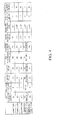
- FIG. 3 is a diagram representing antireflection coating structures of samples that include antireflection coatings of ZrO 2 /SiO 2 (a total of five layers in each antireflection coating).
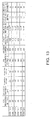
- FIG. 4 is a diagram summarizing the producing conditions and the evaluation results for the conduction processing layer included in the antireflection coating.
- FIG. 5A is a cross sectional view showing how the sheet resistance of a sample surface is measured
- FIG. 5B is a plan view showing how the sheet resistance of a sample surface is measured.
- FIG. 6 is a diagram schematically illustrating the structure of a sample for XPS analysis.
- FIG. 7 is a diagram summarizing the producing conditions and the evaluation results for XPS analysis samples.
- FIGS. 8A and 8B are diagrams representing XPS analysis results, in which FIG. 8A represents an Ar2p spectrum, and FIG. 8B represents a Ti2p spectrum.
- FIG. 9 is a diagram schematically illustrating the structure of a sample for SIMS analysis.
- FIG. 10 is a diagram representing the depth profile measurement result of SIMS targeting Ar.
- FIG. 11 is a diagram schematically representing a sample for reflectance measurement, and a reflectance measurement method.
- FIG. 12 is a diagram representing the result of reflectance measurement.
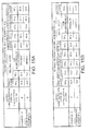
- FIG. 13 summarizes the producing conditions and the evaluation results for samples of other Examples.
- FIG. 14 is a cross sectional view illustrating the structure of a lens that includes a multilayer antireflection coating.
- FIG. 15A is a diagram representing an example of ion bombardment of a second layer
- FIG. 15B is a diagram representing an example of ion bombardment of a sixth layer.
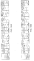
- FIG. 16A is a diagram summarizing the producing conditions and the evaluation results for the samples of the Example and Comparative Example represented in FIG 15A
- FIG. 16B is a diagram summarizing the producing conditions and the evaluation results for the samples of the Example and Comparative Example represented in FIG 15B .
- FIG. 17 is a diagram schematically illustrating eyeglasses.
- FIG. 1 shows a cross sectional configuration of a lens of an embodiment of the invention on one side of the lens relative to the base material at the center.
- a lens (optical article) 10 includes a lens base material (optical base material) 1, a hardcoat layer 2 formed on a surface of the lens base material 1, a translucent, multilayer antireflection coating 3 formed on the hardcoat layer 2, and an antifouling layer 4 formed on the antireflection coating 3.
- the antireflection coating 3 includes a conduction processing layer (first layer) 33 formed on the optical base material 1 via the hardcoat layer 2 and the other layers of the antireflection coating 3.
- the first layer 33 is a translucent layer that contains TiO x (0 ⁇ x ⁇ 2).
- the argon concentration of the first layer 33 is higher on a surface side (surface region) 33a than in a deeper portion (optical base material side) 33b of the first layer 33.
- the first layer 33 containing TiO x (0 ⁇ x ⁇ 2), and having an argon concentration higher in the surface region 33a than in the deeper portion (optical base material side) 33b has sufficient levels of translucency for eyeglass lenses, and is conductive with a low sheet resistance.
- the first layer 33 can typically be produced using a producing method that includes: (1) forming a TiO 2 -containing translucent target layer on the optical base material, either directly or via some other layer; and (2) ionizing and bombarding a mixed gas of argon gas and oxygen gas on a surface of the target layer.
- the present inventors speculate that the ionization and bombardment of the mixed gas of argon gas and oxygen gas on the surface of the TiO 2 -containing target layer forms the first layer 33 with oxygen defects (oxygen losses) in the surface region 33a, and that the oxygen losses in the surface region 33a serve as carriers to develop conductivity. Further, because the mixed gas contains both argon gas and oxygen gas, the ionization and bombardment of the mixed gas is believed to appropriately correct the argon ion-induced oxygen losses by the presence of oxygen ions, and thus suppress a large decrease in light transmittance. Further, the conductivity of the surface region 33a is presumably maintained by argon atoms captured in the surface region 33a.
- the argon concentration in the deeper portion 33b of the first layer 33 is either low or zero.
- the oxygen loss region is thus confined only within the surface region 33a, and is unlikely to affect the translucency of the first layer 33.
- the oxygen defect is also expected to improve conductivity (lower the sheet resistance).
- the properties of metal oxides change greatly when the mol ratio between the metal and oxide are nonstoichiometric.
- metal is present in an amount which is other than the stoichiometric proportion, oxygen vacancies may form, and these may improve conductivity.
- the increased distortion or oxygen vacancy may form a color center and absorb light to impart color or change the refractive index of the layer, lowering translucency. For this reason, it is difficult to obtain only the conductivity improving effect while avoiding discoloration.
- the oxygen defects oxygen losses
- conductivity can be improved while suppressing the adverse effects on the optical and/or physical characteristics of the layer structure.
- the effects of bombarding the ionized gas tend to diminish with time, for example, as the defect recovers.
- the ionization and bombardment of the mixed gas of argon and oxygen on the target layer surface is believed to allow the argon to remain in the surface region 33a over extended time periods.
- the low surface ⁇ resistance state of the first layer 33 achieved by the ionization and bombardment of the mixed gas (low-resistance process, conduction process) is therefore maintained for a long time.
- the lens (optical article) 10 produced thus has superior optical characteristics and further improved conductivity.
- the deterioration of antistatic performance and/or electromagnetic shielding performance proceeds at a very slow rate in the lens 10, and thus the lens 10 can have long-lasting antistatic performance and/or electromagnetic shielding performance. This is considered to be due to the argon being localized in the surface region 33a of the first layer 33 over extended time periods, causing a localized internal stress increase in the first layer 33, and thus suppressing combination of oxygen vacancies, or forming localized levels.
- ITO Indium Tin Oxide
- In (indium) is a scarce metal (rare metal), and is expensive.
- the ITO easily dissolves in acids and alkalis, the use of ITO for eyeglass lenses and other optical articles requiring environment adaptability is not desirable.
- the first layer 33 containing TiO x (0 ⁇ x ⁇ 2) withstands acids and alkalis.
- the lens 10 in addition to being antistatic, can have strong resistance to acids and alkalis such as in sweat, all at low cost.
- the optical article provided by the embodiment of the invention may include an ITO layer. However, because conductivity can be imparted without an ITO layer, the lens 10 can be provided at low cost, and can be used in a wide variety of environments.
- TiO x is formed within TiO 2 by breaking the TiO 2 bonds through irradiation of a several nanometer thick deposited layer of TiO 2 with an argon and oxygen ion beam having an energy of several hundred electronvolts, to thereby form TiO x .
- the following embodiments also describe producing an antistatic optical article with the TiO x serving as carriers to develop conductivity. Though it is desirable to reduce the thickness of TiO x for transparency, when a TiO x layer is too thin, it may be unstable and have lower conductivity as a result of, for example, defect recombination. Thus, the following describes the conditions for maintaining a stable antistatic property over extended time periods. Further, several conditions suited for antistatic eyeglass lens applications will be described through the improvement of durability realized by preventing recombination with appropriate numbers of argon atoms near the oxygen vacancies.
- the lens base material 1 is not particularly limited, and may be (meth) acrylic resin.
- Other examples include allyl carbonate resin such as styrene resin, polycarbonate resin, allyl resin, and diethylene glycol bis (allyl carbonate) resin (CR-39) ; urethane resin obtained by the reaction of vinyl resin, polyester resin, polyether resin, or an isocyanate compound with a hydroxy compound such as diethylene glycol; thiourethane resin as the product of a reaction between an isocyanate compound and a polythiol compound; and transparent resin obtained by curing a polymerizable composition that contains a (thio)epoxy compound having one or more disulfide bonds within the molecule.
- the refractive index of the lens base material 1 is, for example, about 1.60 to 1.75.
- the refractive index of the lens base material 1 is not limited to this, and may be above or below this range.
- the hardcoat layer 2 formed on the lens base material 1 is provided to impart abrasion resistance to the lens 10 (lens base material 1), or to increase the strength of the lens 10 (lens base material 1).
- the material usable for the hardcoat layer 2 include acrylic resin, melamine resin, urethane resin, epoxy resin, polyvinyl acetal resin, amino resin, polyester resin, polyamide resin, vinyl alcohol resin, styrene resin, silicon resin, and mixtures or copolymers of these.
- the hardcoat layer 2 is silicon resin.
- the hardcoat layer 2 can be formed by, for example, applying and curing a coating composition that contains metal oxide fine particles, and a silane compound.
- the coating composition may also include components such as colloidal silica, and a polyfunctional epoxy compound.
- the metal oxide fine particles contained in the coating composition include fine particles of metal oxides such as SiO 2 , Al 2 O 3 , SnO 2 , Sb 2 O 5 , Ta 2 O 5 , CeO 2 , La 2 O 3 , Fe 2 O 3 , ZnO, WO 3 , ZrO 2 , In 2 O 3 , and TiO 2 , and composite fine particles of metal oxides of two or more metals.
- a colloidal dispersion of such fine particles in a dispersion medium for example, water, alcohol, and other organic solvents
- a dispersion medium for example, water, alcohol, and other organic solvents
- a primer layer may be provided between the lens base material 1 and the hardcoat layer 2 to ensure adhesion between the lens base material 1 and the hardcoat layer 2.
- the primer layer is also effective at improving the impact resistance, a drawback of high-refractive-index lens base material.
- the material used for the primer layer include acrylic resin, melamine resin, urethane resin, epoxy resin, polyvinyl acetal resin, amino resin, polyester resin, polyamide resin, vinyl alcohol resin, styrene resin, silicon resin, and mixtures or copolymers of these.
- Urethane resin and polyester resin are preferable as the primer layer used to provide adhesion.
- the hardcoat layer 2 and the primer layer can be formed by applying a coating composition using a dipping method, a spinner method, a spray method, or a flow method, followed by heating and drying at a temperature of 40 to 200°C for several hours.
- the antireflection coating 3 formed on the hardcoat layer 2 is an inorganic antireflection coating or an organic antireflection coating.
- the lens 10 of the present embodiment includes an inorganic antireflection coating.
- the inorganic antireflection coating is typically configured as a multilayer film.
- the multilayer antireflection coating can be formed by, for example, alternately laminating a low-refractive-index layer having a refractive index of 1.3 to 1.6 and a high-refractive-index layer having a refractive index of 1.8 to 2.6.
- the number of layers is preferably about 5 to 7.
- Examples of the inorganic material used for each layer of the antireflection coating include SiO 2 , SiO, ZrO 2 , TiO 2 , TiO, Ti 2 O 3' Ti 2 O 5 , Al 2 O 3 , TaO 2 , Ta 2 O 5 , NdO 2 , NbO, Nb 2 O 3 , NbO 2 , Nb 2 O 5 , CeO 2 , MgO, Y 2 O 3 , SnO 2 , MgF 2 , WO 3 , HfO 2 , and Y 2 O 3 .
- These inorganic materials may be used either alone or as a mixture of two or more.
- the method (producing method) used to form the antireflection coating 3 may be a dry method, for example, such as a vacuum vapor deposition method, an ion plating method, and a sputtering method.
- the vacuum vapor deposition method may use an ion beam-assisted method, in which an ion beam is simultaneously shone during the vapor deposition.
- An organic antireflection coating may be formed in place of the inorganic antireflection coating 3.
- a wet method may be used as the method (producing method) of forming the organic antireflection coating.
- the organic antireflection coating may also be formed by, for example, coating with an antireflection coating composition that contains (i) silica fine particles having inner cavities (hereinafter, also referred to as "hollow silica fine particles"), and (ii) an organosilicon compound, using the same methods used to form the hardcoat layer and the primer layer.
- the reason the hollow silica fine particles are used for the antireflection coating coating composition is that the inner cavities contain a gas or a solvent of lower refractive index than that of silica, and that the lower refractive index than that of silica fine particles having no cavities provides superior antireflection effects.
- the hollow silica fine particles can be produced using, for example, the method described in JP-A-2001-233611 .
- hollow silica fine particles having an average particle size of 1 to 150 nm, and a refractive index of 1.16 to 1.39 are used.
- the thickness of the organic antireflection coating is preferably 50 to 150 nm.
- the antireflection coating 3 includes the first layer 33.
- the first layer 33 contributes to making the lens 10 conductive (low resistance).
- the first layer 33 will be referred to as conduction processing layer 33.
- the first layer 33 may also be called a conduction layer, or a low-resistance layer.
- the basic composition of the conduction processing layer 33 is TiO x (0 ⁇ x ⁇ 2).
- the conduction processing layer (first layer) 33 is formed (configured) on the surface layer of any of the high-refractive-index layers.
- the conduction processing layer (first layer) 33 is formed on at least one of the layers, typically by being laminated on the surface of at least one of the high ⁇ refractive ⁇ index layers.
- the conduction processing layer (first layer) 33 also may be formed by being laminated on the surface of the organic antireflection coating to lower surface resistance.
- the lens 10 includes the multilayer antireflection coating 3 as a laminate of a low-refractive-index layer 31 (SiO 2 ) and a high-refractive-index layer 32 (ZrO 2 ) .
- the antireflection coating 3 has a 5-layer structure including alternately laminated three low-refractive-index layers 31 and two high ⁇ refractive ⁇ index layers 32.
- the conduction processing layer 33 is thus formed by being laminated on any of the high-refractive-index layers 32 (ZrO 2 ) of different compositions.
- the conduction processing layer 33 is provided between the uppermost low ⁇ refractive ⁇ index layer (fifth layer) 31 and the uppermost high ⁇ refractive ⁇ index layer (fourth layer) 32.
- the antireflection coating 3 of basically a 5-layer structure can be said to have a 6-layer structure with the conduction processing layer 33.
- the conduction processing layer 33 of the lens 10 is a translucent layer of TiO x (0 ⁇ x ⁇ 2), containing more argon on the surface side (surface region) 33a.
- the proportion x in the composition TiO x (0 ⁇ x ⁇ 2 ) of the conduction processing layer 33 is not required to be constant throughout the conduction processing layer 33. It is assumed that the surface region 33a contains relatively larger amounts of TiO x1 (x1 ⁇ 1.7 to 1.8) , and that the deeper portion (base material 1 side) 33b contains rel atively larger amounts of TiO x2 (x2 ⁇ 2.0).
- the argon concentration is higher in the surface region 33a than in the deeper portion 33b, forming a concentration gradient or concentration steps in the conduction processing layer 33.
- the conduction processing layer 33 argon-rich on the surface can be produced using a producing method that includes: forming a target layer that contains the main component TiO 2 ; and ionizing and bombarding a mixed gas of argon gas and oxygen gas on the target layer surface.
- the ionization and bombardment of the mixed gas of argon gas and oxygen gas is important.
- the bombardment of the ionized argon gas forms the conduction processing layer 33 that has the surface region 33a of high argon concentration, and the bombardment of the ionized oxygen gas repairs the bombardment-induced defects in surface region 33a to some extent to suppress large deterioration of optical performance. Further, because the detects in the surface region 33a are repaired to some extent, the argon (atoms) can be confined in a stable fashion in the surface region 33a, and the electrical properties of the conduction processing layer 33 can remain stable over extended time periods.
- the ionization and bombardment of the mixed gas of argon gas and oxygen gas causes the oxygen atoms in some of the TiO 2 in the surface region 33a of the target TiO 2 layer to separate or leave, making the stoichiometric ratio of the metal and oxygen atoms out of proportion from the composition of the predetermined compound (i.e creating a nonstoichiometric composition).
- This is believed to create oxygen defects (vacancies due to oxygen losses) in the surface region 33a, the oxygen vacancies serving as carriers to develop conductivity (lower the sheet resistance).
- the argon remains in the localized state in the surface region 33a, recombination of oxygen vacancies can be suppressed, or localized levels are formed.
- the inclusion of the conduction processing layer 33 thus imparts antistatic performance to the antireflection coating 3, and the antistatic performance is maintained over extended time periods. Further, the oxygen loss region in the conduction processing layer 33 is confined only in the surface region 33a, and thus has only small influence on the optical performance of the antireflection coating 3.
- Changes in argon concentration in the conduction processing layer 33 can be measured by secondary ion mass spectrometry (SIMS) performed along the depth direction from the surface of the conduction processing layer 33.
- SIMS secondary ion mass spectrometry
- the analysis method is not limited to this, and any method can be used as long as it is recognized as being effective for analytical purposes.
- Specific values of argon concentration can be measured by using, for example, X ⁇ ray photoelectron spectroscopy (XPS).
- the thickness of the conduction processing layer 33 is not particularly limited, as long as it does not affect the performance of the high ⁇ refractive ⁇ index layers 32.
- the conduction processing layer 33 preferably has a thickness of 4 nm or more, in order to obtain the effect of the conduction process by the bombardment of the ionized mixed gas, and to contain appropriate concentrations of argon in the surface region 33a.
- the thickness of the conduction processing layer 33 is preferably 15 nm or less, because when too thick, it may increase the optical absorption loss.
- a water ⁇ repellent film or a hydrophilic anti-fog film (antifouling layer) 4 is often formed on the antireflection coating 3.
- the antifouling layer 4 is formed as a layer of a fluorine-containing organosilicon compound on the antireflection coating 3 to improve the water-repellency and oil ⁇ repellency of the surface of the optical article (lens) 10.
- Preferred examples of the fluorine-containing organosilicon compound include fluorine ⁇ containing silane compounds.
- the fluorine-containing silane compound is dissolved in an organic solvent, and used as a water-repellent treatment liquid adjusted to a predetermined concentration (antifouling layer-forming coating composition).
- the antifouling layer can be formed by applying the water-repellent treatment liquid (antifouling layer-forming coating composition) on the antireflection coating.
- the method may be, for example, a dipping method, or a spin coating method.
- the antifouling layer also may be formed by a dry method such as a vacuum vapor deposition method, using the water ⁇ repellent treatment liquid (antifouling layer-forming coating composition) charged into a metal pellet.
- the thickness of the antifouling layer 4 having water- and oil ⁇ repellency is not particularly limited, and is preferably from 0.001 to 0.5 ⁇ m, more preferably from 0.001 to 0.03 ⁇ m. It is not preferable to make the thickness of the antifouling layer 4 too thin, because it diminishes the water ⁇ repelling and oil-repelling effect, or to make it too thick as it makes the surface tacky. A thickness of the antifouling layer 4 above 0. 03 ⁇ m may lower the Antireflection effect.
- FIG. 3 summarizes the structure of each antireflection coating 3 of Examples and Comparative Examples.
- FIG. 4 summarizes the conditions used to produce each conduction processing layer 33 of Examples and Comparative Examples, and the evaluation results for these layers.
- An eyeglass plastic lens base material (refractive index 1.67; Seiko Super Sovereign (SSV); Seiko Epson) was used as the lens base material 1.
- the application liquid (coating liquid) for forming the hardcoat layer 2 was prepared as follows. 4.46 parts by weight of an acid anhydride hardener (hardener liquid (C2); Arakawa Chemical Industries, Ltd.) was added to 20 parts by weight of an epoxy resin-silica hybrid (Compoceran E102; Arakawa Chemical Industries, Ltd.), and the mixture was stirred to obtain the application liquid (coating liquid, coating solution). The coating solution was then applied on the lens base material 1 in a predetermined thickness using a spin coater. The lens base material 1 with the coating was calcined at 125°C for 2 hours to deposit the hardcoat layer 2.
- an acid anhydride hardener hardener liquid (C2); Arakawa Chemical Industries, Ltd.
- C2 acid anhydride hardener
- an epoxy resin-silica hybrid Compoceran E102; Arakawa Chemical Industries, Ltd.
- the antireflection coating 3 (type A) for the lens sample S1 of Example 1 was deposited.
- sample S1 the sample of each Example
- sample S1 the sample of each Example
- sample 10 the term “sample 10" will be used to collectively refer to the samples of Examples.
- FIG. 2 illustrates an example of a vapor deposition apparatus 100 that can be used to continuously produce (deposit) the inorganic multilayer antireflection coating 3, and the conduction processing layer 33 provided in the antireflection coating 3.
- the vapor deposition apparatus 100 is an electron beam vapor deposition apparatus, and includes a vacuum vessel 110, an evacuator 120, and a gas supply unit 130.
- the vacuum vessel 110 includes a sample support 115 used to place the lens sample 10 with the hardcoat layer 2 formed (deposited) thereon, a base material-heating heater 116 used to heat the lens sample 10 set on the sample support 115, and filaments 117 that generate thermoelectrons.
- the base material-heating heater 116 is provided as, for example, an infrared lamp, and heats the lens sample 10 to remove gas or moisture, and thus ensures adhesion for the layer formed on the surface of the lens sample 10.
- thermoelectrons 114 bombards thermoelectrons 114 to the material (vapor deposition material) set in evaporation sources (crucibles) 112 and 113, causing the material to evaporate and vapor deposit on the lens sample 10.
- the vapor deposition apparatus 100 also includes an ion gun 118 for ion-assisted vapor deposition.
- the ion gun 118 ionizes and accelerates the gas introduced into the vacuum vessel 110 for bombardment onto the lens sample 10.
- the vacuum vessel 110 may be provided with devices such as a cold trap used to remove the remaining moisture, and a device used to control the thickness. Examples of thickness control device include a reflection ⁇ type optical thickness meter, and a crystal oscillator thickness meter.
- the vacuum vessel 110 may be maintained at a high vacuum, for example, 1 ⁇ 10 -4 Pa, using a turbo molecular pump or a cryopump 121, and a pressure control valve 122 provided in the evacuator 120.
- a predetermined gas atmosphere also may be created inside the vacuum vessel 110 using the gas supply unit 130.
- the gas supply unit 130 includes a gas container 131 ready to supply gases such as argon (Ar), nitrogen (N 2 ), and oxygen (O 2 ).
- the gas flow volume can be controlled using a flow volume controller 132.
- the pressure inside the vacuum vessel 110 can be controlled using a pressure meter 135.
- the vapor deposition conditions of the vapor deposition apparatus 100 basically include vapor deposition material, the acceleration voltage and the current value of the electron gun, and the presence or absence of ion assistance.
- the conditions for ion assistance depend on the type of ions (atmosphere of the vacuum vessel 110), and the voltage and current values of the ion gun 118.
- the acceleration voltage and the current value of the electron gun are selected from the 5 to 10 kV range and the 50 to 500 mA range, respectively, according to such factors as the deposition rate, unless otherwise specified.
- the voltage value and the current value of the ion gun 118 are selected from the 200 V to 1 kV range and the 100 to 500 mA range, respectively, according to such factors as the deposition rate.
- the lens sample 10 with the hardcoat layer 2 was washed with acetone.
- the moisture attached to the lens sample 10 was evaporated by a heat treatment performed at about 70°C inside the vacuum vessel 110.
- an oxygen ion beam was shone on the surface of the lens sample 10 at a several hundred electronvolt energy using the ion gun 118 to remove the organic material adhered on the surface of the lens sample 10.
- This process (method) can also improve the adhesion of the layer (film) formed on the surface of the lens sample 10.
- the same process may be performed using inert gas, for example, such as argon (Ar) gas and xenon (Xe) gas, or using nitrogen (N 2 ), instead of oxygen ions. Irradiation of oxygen radicals or oxygen plasma is also possible.
- the low-refractive-index layers 31 and the high ⁇ refractive ⁇ index layers 32 were alternately laminated to produce the antireflection coating 3, using an electron beam vacuum vapor deposition method.
- silicon dioxide (SiO 2 ) layers were formed as the low-refractive-index layers 31, and zirconium oxide (ZrO 2 ) layers were formed as the high-refractive-index layers 32.
- the first layer, the third layer, and the fifth layer represent the low ⁇ refractive ⁇ index layers 31, and the SiO 2 layers were deposited by vacuum vapor deposition without ion assistance.
- the deposition rate was 2.0 nm/sec, and the acceleration voltage and the current of the electron gun were 7 kV and 100 mA, respectively.
- the first layer, the third layer, and the fifth layer were controlled to have thicknesses of 29 nm, 16 nm, and 91 nm, respectively.
- the second layer and the fourth layer represent the high ⁇ refractive ⁇ index layers 32, and were deposited as ZrO 2 layers by the heat evaporation of tablet ZrO 2 sintered material using an electron beam.
- the deposition rate was 0.8 nm/sec.
- the second layer and the fourth layer were controlled to have thicknesses of 40 nm and 60 nm, respectively.
- the conduction processing layer 33 was deposited after the deposition of the fourth layer (ZrO 2 ) 32, before depositing the fifth layer (SiO 2 ) 31.
- the target TiO 2 layer (thickness, 8 nm) was deposited on the fourth layer by ion-assisted vapor deposition with the introduced oxygen gas.
- the deposition rate was 0.4 nm/sec
- the voltage of the irradiated ion beam (ion acceleration voltage) was 500 V
- the ion beam current was 200 mA.
- Oxygen gas (O 2 gas; 35 sccm) was used as the introduced gas to the ion gun (where sccm stands for "standard cubic centimeter per minute”).
- Oxygen gas (O 2 gas; 15 sccm) was also used as the introduced gas to the vacuum vessel (chamber) 110.
- a mixed gas of argon gas and oxygen gas was ionized and bombarded on the surface of the target TiO 2 layer using the vapor deposition apparatus (vacuum vapor deposition apparatus) 100 to alter the target TiO 2 layer to the conduction processing layer 33.
- the gas introduced to the ion gun is the mixed gas of argon gas and oxygen gas, and contains 16.5 sccm of argon gas (Ar gas), and 3.5 sccm of oxygen gas (O 2 gas) (a mixture ratio of about 4.7:1) .
- the irradiation (process) was performed for 30 seconds with the 800-V of the irradiated ion beam (ion acceleration voltage) and the 200 ⁇ mA ion beam current.
- a pellet material containing "KY-130" (Shin-Etsu Chemical Co., Ltd.) that contains a large-molecular-weight fluorine ⁇ containing organosilicon compound was used as the deposition source and heated at about 500°C in the vacuum vessel 110 to evaporate the KY-130 and deposit the antifouling layer 4 on the antireflection coating 3 (on the final SiO 2 layer 31 of the antireflection coating 3) .
- the vapor deposition time was about 3 minutes.
- the lens sample 10 was taken out of the vacuum vapor deposition apparatus 100, flipped over, and placed in the apparatus again, where the steps 2.1.2.2 to 2.1.2.4 and the step 2.1.3 were repeated in the same procedure to deposit the antireflection coating 3 and the antifouling layer 4.
- the lens sample 10 was then taken out of the vacuum vapor deposition apparatus 100.
- the resulting lens sample S1 of Example 1 thus included the hardcoat layer 2, the antireflection coating 3 (type A1), and the antifouling layer 4 on each side of the lens base material 1.
- Samples S2 and S3 of Examples 2 and 3 were produced in the same manner as in sample S1 of Example 1. Note, however, that the irradiation time of the ionized mixed gas in the conduction processing layer-forming step 2.1.2.4 was 120 seconds for sample S2 of Example 2. For sample S3 of Example 3, the irradiation time of the ionized mixed gas in the conduction processing layer-forming step 2.1.2.4 was 240 seconds. The other conditions for these samples are the same as in Example 1.
- Samples R1 and R2 of Comparative Examples 1 and 2 were produced for comparison with the samples obtained in Examples.
- vapor deposition material (Patinal Titanium Oxide S TiO 1.7 ; MERCK) was used. The material was melted and evaporated in a vacuum (in the vacuum vessel 110) by electron beam heating. The acceleration voltage and the current of the electron gun were 6 kV and 270 mA, respectively. No gas was introduced to the chamber (vacuum vessel) 110, and ion assistance was not used. The conduction processing layer was deposited only with a TiO 1.7 steam, and the deposition of a 8-nm thick TiO 1.7 film took 50 seconds.
- Sample R2 of Comparative Example 2 was produced by ionizing and bombarding only the argon gas on the surface of the target TiO 2 layer in the conduction processing layer ⁇ forming step 2.1.2.4.
- argon gas Ar gas
- All the other conditions for these samples are the same as in Example 1.
- the samples S1 to S3 and the samples R1 to R2 produced as above were measured for optical absorption loss and initial sheet resistance value, and the antistatic property (initial) and the durability of antistatic property were evaluated.
- optical absorption loss was measured using samples prepared to include the conduction processing layer 33 in the antireflection coating 3, and the antifouling layer 4 formed in the steps described above, using parallel flat glass as the base material. The hardcoat layer was not deposited in these samples.
- the optical absorption loss was found by calculating absorption from the measured reflectance and transmittance, according to the following equation (A).
- Spectrophotometer U ⁇ 4100 Hitachi was used for the measurement.
- Absorption (absorption loss) 100% - transmittance - reflectance ...(A)
- the absorption is the absorption near 550 nm wavelength.
- FIG. 4 summarizes the measurement results. The values of optical absorption loss were 1% or less in Samples S1 to S3 of Examples 1 to 3 and in sample R1 of Comparative Example 1. It is thus believed that translucency is sufficiently high, and that there is no large influence on the translucency of the antireflection coating 3.
- the value of optical absorption loss was as high as 2.26% in sample R2 of Comparative Example 2, in which only the argon gas was ionized and bombarded on the surface of the target TiO 2 layer. It was therefore found that the optical absorption loss could be reduced by the ionization and bombardment of the mixed gas of argon and oxygen.
- FIGS. 5A and 5B show how the sheet resistance of each sample was measured.
- the sheet resistance on a surface 10F of the lens sample 10 was measured with a ring probe 61 in contact with the surface 10F of the lens sample 10 being measured.
- High-resistance resistivity meter Hiresta UP (Model MCP-HT450; Mitsubishi Chemical Corporation) was used as a measurement device 60.
- the ring probe 61 is of an URS type, and includes two electrodes.
- An outer ring electrode 61A has an outer diameter of 18 mm, and an inner diameter of 10 mm.
- An inner circular electrode 61B has a diameter of 7 mm.
- the sheet resistance of each sample was measured by applying a voltage of 100 V to 10, 000 V between these electrodes.
- FIG. 4 summarizes the measurement results.
- Samples S1 to S3 of Examples 1 to 3 had sheet resistances of 1 x 10 10 [ ⁇ / ⁇ ], 4 x 10 8 [ ⁇ / ⁇ ], and 3 x 10 8 [ ⁇ / ⁇ ], respectively.
- the sheet resistance of sample R2 of Comparative Example 2 was 6 x 10 5 [ ⁇ / ⁇ ], an even lower resistance.
- the optical absorption loss was large, the use of the lens 10 may be limited to applications where a large optical absorption loss can be tolerated, for example, as in sunglasses.
- a sheet resistance of 1 x 10 12 [ ⁇ / ⁇ ] or less is regarded as the indicator that determines the presence or absence of antistatic property in eyeglasses lenses.
- an eyeglasses lens can be deemed as being antistatic when it has a sheet resistance of 1 x 10 12 [ ⁇ / ⁇ ] or less.
- the sheet resistance measured by the foregoing method is more preferably 1 x 10 11 [ ⁇ / ⁇ ] or less.
- Samples S1 to S3 all have sheet resistances of 1 x 10 11 [ ⁇ / ⁇ ] or less as measured by the foregoing method, and are thus can be said as being safe for use, and having an excellent antistatic property.
- the antistatic property and the durability of antistatic property were evaluated as follows.
- samples S1 to S3 of Examples 1 to 3 were evaluated as Good, sample R1 of Comparative Example 1 as Acceptable, and sample R2 of Comparative Example 2 as Good, showing that the samples all have antistatic property, including sample R1 of Comparative Example 1.
- Each sample was stored in 60°C, 98% RH conditions, and changes (deterioration) in sheet resistance were examined. Specifically, the time for the sheet resistance of each sample to reach 1 x 10 12 [ ⁇ / ⁇ ] was measured, and the durability was determined according to the length of the measured time, according to the following criteria. Excellent: 350 hours or more Good: 250 hours or more, less than 350 hours Acceptable: 100 hours or more, less than 250 hours Poor: Less than 100 hours
- the durability was 100 hours or more in samples S1 to S3 of Examples 1 to 3, and 350 hours or more in samples S2 and S3 of Examples 2 and 3.
- the durability was not much different in this range, as demonstrated by sample R2 of Comparative Example 2 which also had a durability of 350 hours or more.
- the conduction processing layer 33 formed by the ionization and bombardment of the mixed gas of argon gas and oxygen gas on the surface of the target TiO 2 layer could lower sheet resistance, and provide the static charge preventing and electromagnetic shielding effects. These effects were also found to be long lasting.
- Samples S1 to S3 of Examples 1 to 3 were evaluated for chemical resistance and swelling.
- Chemical resistance was evaluated by observing the presence or absence of peeling of the antireflection coating from the sample surface immersed in a chemical solution after being scratched. More specifically, chemical resistance was evaluated after the abrasion step and chemical immersion step performed as follows.
- evaluation samples 10 were attached to the inner wall of a container (drum), and a nonwoven fabric and sawdust were placed in the container to create abrasion.
- the container was capped, and the drum was rotated at 30 rpm for 30 minutes.
- a chemical solution mimicking human sweat was prepared (a solution of 50 g/L lactic acid and 100 g/L salt dissolved in deionized water) . Samples 10 after the abrasion step (1) were then immersed for 100 hours in the chemical solution maintained at 50°C.
- Moisture resistance was evaluated by a constant-temperature constant-humidity environment test. Specifically, samples S1 to S3 and samples R1 and R2 were left unattended in a constant-temperature constant-humidity environment (60°C, 98% RH) for 8 days, and evaluated according to the following criteria.
- the presence or absence of swelling was determined by observing the reflected light off the front or back surface of each sample subjected to the constant-temperature constant-humidity environment test. Specifically, the fluorescence reflected light off the convex face of each sample was observed, and the sample was determined as having "no swelling" when clear, defined outlines were observed in the fluorescence reflected light image. On the other hand, the sample was determined as having "swelling" when the outlines of the fluorescence reflected light image appeared blurry or dim.
- samples S1 to S3 of Examples 1 to 3 had antistatic properties and antistatic property durability, and the level of transparency was sufficient for use as an article such as an eyeglass lens.
- Samples S2 and S3 of Examples 2 and 3 were found to be particularly durable in terms of antistatic property. From the foregoing, it is considered preferable that the mixed gas of argon gas and oxygen gas be ionized and bombarded on the surface of the target TiO 2 layer for 120 seconds or more (ion beam irradiation time) in the conduction process (2.1.2.4).
- the state of the conduction processing layer 33 was confirmed by X-ray photoelectron spectroscopy (XPS), secondary ion mass spectrometry (SIMS), and reflectance measurement.
- XPS X-ray photoelectron spectroscopy
- SIMS secondary ion mass spectrometry
- Samples X1 to X3 for XPS analysis corresponding to samples S1 to S3 of Example 1 to 3, were produced to confirm the argon concentration in the surface region 33a in the conduction processing layer 33 by XPS analysis.
- samples X1 to X3 for XPS analysis were produced by forming the conduction processing layer 33 under the same deposition conditions (2.1.2.4) used for the conduction processing layers 33 of Examples 1 to 3, using a silicon wafer (Si(100)) as the base material.
- the target TiO 2 layer (thickness, 8 nm) was formed, and the mixed gas of argon gas and oxygen gas was ionized and bombarded by ion-assisted vapor deposition performed with the introduced oxygen gas. Note that the sheet resistance of the conductive layer itself cannot be measured because of the low resistivity of the silicon wafer (Si(100)). Thus, the conduction processing layer 33 was deposited on a glass substrate using the same procedure described above, and the electrical properties were confirmed.
- the results of XPS analysis at the photoelectron escape angle of 45° are believed to relatively reflect the state of the surface region 33a of the conduction processing layer 33.
- the XPS analysis thus revealed the presence of 2. 0% or more argon atoms in the surface regions 33a of the conduction processing layers 33 of samples X1 to X3 of Examples 1 to 3.
- the argon concentration in the surface region 33a of the conduction processing layer 33 typically the concentration of argon atoms determined by XPS analysis was preferably 2.0% or more, in order to obtain antistatic property.
- the preferred argon concentration in the surface region 33a of the conduction processing layer 33 was found to be 2.2% or more, further preferably 2.5% or more.
- FIGS. 8A and 8B represent an example of spectra obtained by XPS analysis for sample X2.
- the horizontal axis represents binding energy (bonding energy; eV), and the vertical axis represents photoelectron counts per second (c/s).
- the spectrum of a sample analyzed by XPS with a laminated target TiO 2 is indicated by broken line.
- the horizontal axis represents binding energy (bonding energy; eV), and the vertical axis represents the normalized photoelectron intensity (normalized intensity).
- the spectrum of a sample analyzed by XPS with a laminated target TiO 2 is indicated by broken line.
- the ionization and bombardment of the mixed gas of argon gas and oxygen gas in the target TiO 2 layer forms the conduction processing layer 33 that includes argon gas in the surface region 33a, and the low-valency-state Ti, specifically TiO x (0 ⁇ x ⁇ 2), at least in the surface region 33a.
- Sample SM2 for SIMS analysis corresponding to sample S2 of Example 2, was produced to confirm the argon concentration in the surface region 33a of the conduction processing layer 33 by SIMS analysis.
- sample SM2 for SIMS analysis was produced by forming a 10-nm thick ZrO 2 layer 32 under the deposition conditions (2.1.2.3) of the high-refractive-index layer of Example 2, using a silicon wafer (Si(100)) as the base material, and by forming a 10-nm thick ZrO 2 layer 32 after forming the conduction processing layer 33 under the deposition conditions (2.1.2.4) of the conduction processing layer 33.
- the target TiO 2 layer in the conduction processing layer 33 had a thickness of 10 nm. Specifically, the target TiO 2 layer was formed in a thickness of 10 nm, and the mixed gas of argon gas and oxygen gas was ionized and bombarded to form the conduction processing layer 33.
- the upper ZrO 2 layer 32 is formed to suppress contamination and oxidation on the surface of the conduction processing layer 33, and the elimination of Ar.
- FIG. 10 represents the result of the depth profile measurement by SIMS analysis targeting Ar.
- the etching element cesium ions were bombarded on sample SM2 at 1.5 kV, 50 nA, and the etched component was analyzed, using PHI/Adept-1010.
- FIG. 10 also represents the depth profile (broken line) of a comparative sample produced by forming a 10-nm thick TiO 2 layer and without bombarding the ionized mixed gas.
- the horizontal axis represents time (seconds), and the vertical axis represents target secondary ion ( 40 Ar + 113 Cs) + ion (173 amu) counts per second (c/s).
- the target secondary ions, ( 40 Ar + 113 Cs) + ions (173 amu), are counted over the background of other ions such as ( 94 Zr + 46 Ti + 17 O + 16 O) + ions (173 amu) (mass interference).
- the depth profile of sample SM2 is believed to be the synthesis of the relatively sharp peak at a portion (near 150 seconds to 250 seconds) corresponding to the surface region 33a of the conduction processing layer 33, and a near trapezoidal peak at a portion (near 150 seconds to 400 seconds) corresponding to the whole of the conduction processing layer 33.
- the depth profile of the comparative sample only has a near trapezoidal peak at a portion (near 150 seconds to 400 seconds) corresponding to the whole of the TiO 2 layer. It is thus believed that the near trapezoidal peak at a portion (near 150 seconds to 400 seconds) corresponding to the whole of the conductive layer 33 and the TiO 2 layer is the background peak, and that the relatively sharp peak at a portion (near 150 seconds to 250 seconds) corresponding to the surface region 33a is the ( 40 Ar + 113 Cs) + ion peak. It can be seen from this that the argon peak can be found by normalizing the SIMS depth profile by the second half of the near trapezoidal peak that appears at a portion corresponding to the deeper portion of the conductive layer 33 and the TiO 2 layer.
- the argon concentration in the conduction processing layer 33 was higher on the surface side (surface region) 33a than in the deeper portion (optical base material side) 33b.
- the gradient or steps in the argon concentration in the conduction processing layer 33 can be confirmed by the argon peak that appears on the surface side (surface region) 33a in the spectrum obtained by SIMS (secondary ion mass spectrometry) performed along the depth direction of the conduction processing layer 33 from the surface.
- SIMS secondary ion mass spectrometry
- Sample SL3, corresponding to sample S3 of Example 3, was produced for the measurement of reflectance changes, in order to confirm changes in the state of the conduction processing layer 33 during the ionization and bombardment of the mixed gas for layer formation.
- sample SL3 was produced by forming the conduction processing layer 33 on a white glass (B270; Schott) substrate under the deposition conditions (2.1.2.4) of the conduction processing layer 33.
- a target TriO 2 layer having a thickness of 8 nm was formed in sample SL3, and changes in reflectance during the formation of the conduction processing layer 33 undergoing the bombardment of the ionized mixed gas of argon gas and oxygen gas under the conditions of Example 3 were measured.
- FIG. 12 represents the result of reflectance measurements.
- the reflectance measurements used an optical thickness meter (OPM-8; Shincron Co., Ltd.), and the reflectance of 440-nm wavelength light was measured.
- the light incident angle was set to 5° with respect to the normal line of the substrate.
- the reflectance is not a measure of the transmissivity of the conduction processing layer 33, but a measure by which the presence or absence of physical property changes is confirmed for the conduction processing layer 33 bombarded with the ionized gas. Accordingly, the measurement is intended to find relative changes in reflectance over time.
- FIG. 12 thus represents changes in reflectance relative to the reflectance 100 at the start of bombardment.
- This result combined with the results of Examples 1 to 3 ( FIG. 4 ) and the result of XPS analysis ( FIG. 7 ), suggests that the argon concentration in the surface region 33a shows a very abrupt increase following about 30 seconds of the irradiation of the mixed gas ion beam, before it substantially levels off after about 100 seconds of bombardment, and shows a very little increase after about 120 seconds.
- the bombardment of the ionized mixed gas (ion beam irradiation time) for the formation of the conduction processing layer 33 was preferably 30 seconds or more, more preferably 100 seconds or more, further preferably 120 seconds or more.
- the sample (including the conduction processing layer 33) under the ion beam may rise to a temperature of several ten degrees, or to a temperature above the heat resistant temperature in the case of plastic base material. Because the argon concentration is believed to show a very little increase after 120 seconds of irradiation, the ion beam irradiation time is preferably 300 seconds or less.
- Samples S4 to S9 of Examples 4 to 9 were produced in the same manner as for sample S1 of Example 1.
- samples S4 to S9 were produced under the same conditions used in Example 1, except that the thickness of the target TiO 2 layer was varied in the deposition of the conduction processing layer (2.1.2.4), and that the bombardment of the ionized mixed gas was performed for 120 seconds (ion beam irradiation time) in all samples.
- the TiO 2 layer had a thickness of 4 nm for sample S4, 6 nm for sample S5, 8 nm for sample S6, 10 nm for sample S7, 12 nm for sample S8, and 15 nm for sample S9.
- FIG. 13 summarizes the producing conditions and the evaluation results for samples S4 to S9 of Examples 4 to 9.
- Samples S4 to S9 were measured for optical absorption loss and initial sheet resistance value, and evaluated for antistatic property (initial) and the durability of antistatic property. Note that the measurements and evaluation were performed in the same manner as for samples S1 to S3, and will not be described.
- Samples S4 to S9 of Examples 4 to 9 were found to be 0.23%, 0.49%, 0.74%, 0.91%, 1.1%, and 1.4%, respectively, all confined within the range of around 1%.
- Samples S4 to S9 had sheet resistances of 5 x 10 10 [ ⁇ / ⁇ ], 1 x 10 9 [ ⁇ / ⁇ ], 3 x 10 8 [ ⁇ / ⁇ ], 2 x 10 8 [ ⁇ / ⁇ ], 1x 10 8 [ ⁇ / ⁇ ], and 8 x 10 7 [ ⁇ / ⁇ ] , below the value (1 x 10 11 [ ⁇ / ⁇ ] ) that represents a desirable antistatic property.
- Samples S4 to S9 all had excellent initial antistatic property, and desirable antistatic property durability. Samples with thicknesses of 6 nm and greater had particularly high antistatic property durability, and there was no decrease in antistatic property in samples with thicknesses of 8 nm and greater.
- the thickness of the target TiO 2 layer bombarded with the ionized mixed gas for the formation of the conduction processing layer 33 was preferably 4 nm or more, more preferably 5 nm or more, further preferably 6 nm or more, and most preferably 8 nm or more. Note that considering the adverse effects on absorption loss or on the optical characteristics of the multilayer antireflection coating, the thickness of the target TiO 2 layer, specifically the thickness of the conduction processing layer 33 is 15 nm or less, when the conduction processing layer 33 is formed independently from the high-refractive-index layer of other composition.
- Samples S4 to S9 of Examples 4 to 9 were also evaluated for chemical resistance and swelling as in samples S1 to S3 of Examples 1 to 3. The evaluation results were desirable (Good) for both chemical resistance and swelling.
- FIG. 14 represents an example of the invention applied to a different type of antireflection coating.
- a lens (optical article) 10b includes a lens base material (optical base material) 1, a hardcoat layer 2 formed on a surface of the lens base material 1, a multilayer antireflection coating 3 formed on the hardcoat layer 2, and an antifouling layer 4 formed on the antireflection coating 3.
- FIGS. 15A and 15B represent layer structures of the samples of Example 10 and Comparative Example 3 described below.
- the Antireflection coating 3 has a 7-layer structure, in which four low-refractive-index layers 31 (SiO 2 ) and three high-refractive-index layers 32 (TiO 2 ) are alternately laminated.
- the lowermost high-refractive-index layer (second layer) 32 also serves as the first layer (conductive layer, conduction processing layer) 33, representing an example in which the conduction processing layer 33 is formed on the surface side of one of the high-refractive-index layers of the same composition.
- Example 10 (Sample S10), Example 11 (Sample S11)
- samples S10 and S11 were produced in the same manner as in Example 1, except for the deposition of the low-refractive-index layers and high-refractive-index layers (2.1.2.3), and the deposition of the conduction processing layer (2.1.2.4).
- the antireflection coating 3 includes SiO 2 low-refractive-index layers 31 representing the first, third, fifth, and seventh layers, which were deposited under the same deposition conditions (2.1.2.3) used for the low-refractive-index layer of Example 1, except that the thickness was set to have values presented in FIGS. 15A and 15B .
- the second, fourth, and sixth layers in the antireflection coating 3 of sample S10 are high-refractive-index TiO 2 layers 32, which were deposited under the same conditions used for the target TiO 2 layer irradiated with the ion beam for the deposition of the conduction processing layer of Example 1 (2.1.2.4). Specifically, the TiO 2 layers were deposited by ion-assisted vapor deposition with the introduced oxygen gas. The deposition rate was 0.4 nm/sec, and the acceleration voltage and the current of the electron gun were 7 kV and 360 mA, respectively. Oxygen was used as the ion species for the ion assistance, which was performed at an ion assist voltage of 500 V under 150 mA current. The second, fourth, and sixth layers were controlled to have thicknesses of 13.3 nm, 46.0 nm, and 37.5 nm, respectively.
- the mixed gas of argon gas and oxygen gas was ionized and bombarded on the surface of the deposited second TiO 2 layer (lowermost high-refractive-index layer) during the formation of the antireflection coating 3 of sample S10.
- the same deposition conditions (2.1.2.4) used for the conduction processing layer of Example 1 were used except for the mixed gas ratio and the irradiation time.
- the mixed gas introduced to the ion gun contained 15 sccm of argon gas (Ar gas), and 5 sccm of oxygen gas (O 2 gas) in a 3:1 mixture ratio.
- the ion beam irradiation time was 120 seconds.
- the mixed gas of argon gas and oxygen gas was ionized and bombarded on the surface of the deposited sixth TiO 2 layer 32 (uppermost high-refractive-index layer) during the formation of the antireflection coating 3 of sample S11.
- the same deposition conditions (2.1.2.4) used for the deposition of the conduction processing layer of Example 1 were used except for the mixed gas ratio and the irradiation time.
- the mixed gas introduced to the ion gun contained 10 sccm of argon gas (Ar gas) and 10 sccm of oxygen gas (O 2 gas) in a 1:1 mixture ratio.
- the ion beam irradiation time was 120 seconds.
- the proportions (mixture ratio) of the argon gas and oxygen gas in the mixed gas are preferably 10:1 to 1:2.
- a mixture ratio exceeding 10:1 promotes defect formation with the excess argon, and the low oxygen slows the defect recovery and thus tends to lower transparency.
- a mixture ratio below 1:2 makes it difficult to obtain antistatic performance because of the excessively low argon.
- the preferred mixture ratio is from 5:1 to 1:1. Note that the high-refractive-index TiO 2 layers 32 used for the conduction process are not limited to the lowermost layer (second layer) and the uppermost layer (sixth layer).
- FIG. 16A summarizes the producing conditions and the evaluation results for samples S10 and R3.
- FIG. 16B summarizes the producing conditions and the evaluation results for samples S11 and R4.
- Samples S10 and S11 and samples R3 and R4 were measured for optical absorption loss and initial sheet resistance value, and evaluated for antistatic property (initial) and antistatic property durability. The measurements and evaluation were performed in the same manner as for samples S1 to S3.
- Sample S10 of Example 10 had a optical absorption loss of 0.75%, and sufficiently high translucency. In terms of performance, differences from sample R3 of Comparative Example 3 were small. Sample S10 of Example 10 had a sheet resistance of 1 x 10 9 [ ⁇ / ⁇ ], a value smaller than the evaluation reference value 1 x 10 11 [ ⁇ / ⁇ ] for antistatic property. The evaluation result for antistatic property was thus desirable (Good). Sample S10 also has antistatic property durability. On the other hand, sample R3 of Comparative Example 3 had a sheet resistance of 1 x 10 13 [ ⁇ / ⁇ ] , and was evaluated as having a poor antistatic property.
- Sample S11 of Example 11 had a optical absorption loss of 0.90%, and sufficiently high translucency. In terms of performance, differences from sample R4 of Comparative Example 4 were small. Sample S11 of Example 11 had a sheet resistance of 2 x 10 9 [ ⁇ / ⁇ ] , a value smaller than the evaluation reference 1 x 10 11 [ ⁇ / ⁇ ] for antistatic property. The evaluation result for antistatic property was thus desirable (Good). Sample S11 also had antistatic property durability. On the other hand, sample R4 of Comparative Example 4 had a sheet resistance of 1 x 10 13 [ ⁇ / ⁇ ] , and was evaluated as having a poor antistatic property.
- samples S10 and S11 of Examples 10 and 11 and samples R3 and R4 of Comparative Examples 3 and 4 were also evaluated for chemical resistance and swelling as for samples S1 to S3 of Examples 1 to 3.
- the evaluation results were desirable (Good) for both chemical resistance and swelling.
- TiO z (0 ⁇ z ⁇ 2) has conductivity, and that this material develops conductivity as the oxygen losses (defects) serve as carriers.
- the conductivity decreases with decrease in defect concentration as recombinations take place.
- a stable TiO z film can be obtained by increasing the thickness or by reducing the z value but at the expense of transparency. It has thus been difficult to use the material for antistatic films (such as eyeglass lenses) that require transparency.
- the invention as described above, enables formation of the conductive, low-resistance layer (conduction processing layer, first layer) 33 having a reduced surface electrical resistance, by ionizing and bombarding a mixed gas of argon gas and oxygen gas on the target TiO 2 layer having a relatively thin thickness.
- SIMS analysis confirmed that the concentration of argon atoms in the conduction processing layer 33 was higher on the surface side (surface region) 33a than on the base material side (deeper portion) 33b.
- the ionization and bombardment of the mixed gas of argon gas and oxygen gas on the surface of the TiO 2 -containing target layer creates oxygen defects (oxygen losses) in the surface region 33a, and that the oxygen losses in the surface region 33a serve as carriers to develop conductivity.
- the oxygen ions in the ionized mixed gas are believed to appropriately correct the argon ion-induced oxygen losses, and suppress a large decrease in light transmittance. It is also believed that the oxygen ions help create a state in which the argon atoms are captured in the surface region 33a. It is thus considered possible to form the conduction processing layer 33 in which the argon atoms can stably remain in the surface region 33a, and to thus maintain the antistatic property over extended time periods.
- the argon atoms are believed to be localized in the TiO 2 thin film with the adjacent tetravalent or lower titanium in the form of TiO z (0 ⁇ z ⁇ 2) . Further, because of the stable presence of argon atoms, the TiO z is believed to also remain stable for stable conductivity.
- the conduction processing layer 33 sufficiently satisfies the transparency, conductivity, and durability required of eyeglass lenses.
- a lens can be provided that has effects and functions obtained by the development of conductivity, including the antistatic function, and the electromagnetic wave shielding function.
- the low resistance process (conduction process) described herein is the process that has hardly any adverse effects on the optical functions of the conduction processing layer and of the functional layers including the conduction processing layer, and does not additionally require the optically detrimental lamination of thick conductive layers.
- antistatic performance can be obtained without forming an ITO layer, which can cause deterioration of chemical resistance and moisture resistance, or without basically changing the design of the multilayer film forming the antireflection coating.
- the surface resistance can be lowered without essentially changing the configuration, material, and vapor deposition process used for the Antireflection coating of related art.
- the low resistance process is therefore readily applicable to a wide variety of optical articles at low cost.
- the layer structures of the antireflection coating described in the foregoing Examples are merely examples, and the invention is not restricted by these layer structures.
- the invention is also applicable to an antireflection coating of three or fewer layer structure, or to an antireflection coating of nine or more layer structure, and more than one layer can be subjected to the low resistance process.
- the combination of the high-refractive-index layers and the low-refractive-index layers of the antireflection coating is not limited to TiO 2 /SiO 2 and ZrO 2 /SiO 2 , and may be, for example, Ta 2 O 5 /SiO 2 , NdO 2 /SiO 2 , HfO 2 /SiO 2 , or Al 2 O 3 /SiO 2 .
- the surface layer of any of the layers in such combinations can be processed.
- the invention is applicable to both inorganic antireflection coatings and organic antireflection coatings.
- FIG. 17 illustrates eyeglasses 200 that include an eyeglass lens 10 and a frame 201 attached to the eyeglass lens 10.
- the antistatic property of the eyeglass lens 10 has been improved by the ion bombardment.
- the invention is not limited to eyeglass lenses.
- One other aspect of the invention is a system that includes the optical article, and an apparatus that projects and/or acquires images through the optical article.
- a typical example of the system that includes an apparatus for projection purposes is a projector.
- the optical article is typically, for example, a projection lens, a dichroic prism, or a cover glass.
- the technique described herein is also applicable to the light valve and other elements of LCDs (liquid crystal devices), an example of an image forming apparatus.
- the technique is also applicable to a system, such as a camera, used to acquire images through an optical article.
- the optical article is typically, for example, an imaging lens, or a cover glass.
- the technique also can be used for imaging devices such as CCD.
- the technique is also applicable to an information recording apparatus such as DVD that accesses the information source through an optical article.
Landscapes
- Chemical & Material Sciences (AREA)
- Physics & Mathematics (AREA)
- General Physics & Mathematics (AREA)
- Optics & Photonics (AREA)
- Chemical Kinetics & Catalysis (AREA)
- Organic Chemistry (AREA)
- Engineering & Computer Science (AREA)
- Materials Engineering (AREA)
- Mechanical Engineering (AREA)
- Metallurgy (AREA)
- Toxicology (AREA)
- Health & Medical Sciences (AREA)
- Inorganic Chemistry (AREA)
- Surface Treatment Of Optical Elements (AREA)
- Eyeglasses (AREA)
- Physical Vapour Deposition (AREA)
Abstract
Description
- This application claims priority to Japanese Patent Application No.
2010―173381, filed August 2, 2010 - The present invention relates to optical articles for use in optical materials and products, including lenses such as an eyeglass lenses, and to methods for producing such optical articles.
- A known variation of optical articles such as an eyeglass lens is one that includes various functional layers (films) formed on an optical base material. Known examples of such layers include a hardcoat layer that ensures durability for the optical base material, and an antireflection coating that prevents ghosts and flickers.
-
JP-A-004-341052 - It is known to form a conductive layer of a certain thickness on the layer formed on the optical base material, in order to impart conductivity for antistatic and electromagnetic shielding purposes. An ITO (Indium Tin Oxide) layer is a common example of such a conductive layer. A problem of ITO, however, is that it is relatively expensive, and raises the manufacturing cost.
- Further, the addition of a conductive layer of a certain thickness for the film or layer (for example, a multilayer antireflection coating) produced according to the predetermined optical or film design necessitates a new optical design or film design.
- An aspect of the invention is directed to an optical article that comprises: an optical base material; and a translucent first layer that contains TiOx (0 < x ≤ 2), the first layer being formed on the optical base material either directly or via another layer, and first layer having a surface side and a side facing the optical base material, the first layer having a higher argon concentration on the surface side than on the side facing the optical base material side (deeper portion) of the first layer.
- The present inventors found that the TiOx (0 < x ≤ 2)-containing translucent first layer having a higher argon concentration on the surface layer side has both translucency and conductivity, and can impart antistatic performance and/or electromagnetic shielding performance to the optical article. According to this aspect of the invention, an optical article, such as an eyeglass lens, that has antistatic performance and/or electromagnetic shielding performance, with or without the lamination of ITO (Indium Tin Oxide) is provided.
- The optical article is typically one in which an argon peak appears on the surface side in a spectrum obtained by secondary ion mass spectrometry (SIMS) performed for the first layer along the depth direction from the surface of the first layer. The optical article may be such that a spectrum corresponding to an atomic weight of argon atoms in the first layer after being normalized by a spectrum in the optical base material side of the first layer in SIMS analysis has a peak that appears on the surface side.
- In the optical article, the argon atom concentration on the surface side of the first layer is preferably at least 2.0% as measured by X―ray photoelectron spectroscopy (XPS), because it helps produce the antistatic effect. The argon atom concentration on the surface side of the first layer as measured by XPS is preferably 2.2% or more, more preferably 2.5% or more.
- Further, in the optical article, the first layer has a thickness of preferably at least 4 nm, because it helps produce the antistatic effect. The thickness of the first layer is more preferably 5 nm or more, more preferably 8 nm or more.
- The first layer may be a single layer, or one layer in a multilayer structure layer. The multilayer structure layer is typically a multilayer antireflection coating. The optical article may include a multilayer antireflection coating, and the first layer may be a layer included in the multilayer antireflection coating. The optical article may further include an antifouling layer formed on the first layer either directly or via some other layer.
- The optical base material is typically a plastic lens base material. One form of the optical article is an eyeglass lens, and another aspect of the invention is directed to eyeglasses that include an eyeglass lens, and a frame attached to the eyeglass lens.
- Still another aspect of the invention is directed to a method of manufacturing an optical article.
- The method comprises: forming a TiO2―containing translucent target layer on the optical base material either directly or via another layer; and ionizing and bombarding a mixed gas of argon gas and oxygen gas on the surface of the target layer.
- The method enables the target layer to be changed (converted) to a TiOx (0 < x ≤ 2) ―containing translucent first layer that has an argon concentration which is higher on the surface side of the first layer than on the side of the first layer which is facing the optical base material , and can thus produce an optical article provided with such a first layer. The method thus enables the production and supply of an optical article that has sufficient translucency for articles such as eyeglass lenses, and antistatic performance and/or electromagnetic shielding performance.
- In the optical article producing method, the target layer may be one of the layers included in the multilayer antireflection coating. Further, the optical article producing method may include forming an antifouling layer on the bombarded target layer, specifically, on the first layer, either directly or via some other layer.
- In the optical article production method, it is preferable that the mixed gas be bombarded for 30 seconds to 300 seconds (hereinafter, "irradiation time"). It becomes difficult to obtain antistatic performance with an irradiation time below 30 seconds. An irradiation time above 300 seconds (5 min) is not preferable, because it may increase the temperature of the optical base material too high, and raises the manufacturing cost of the optical article. The irradiation time is more preferably 100 seconds to 300 seconds, further preferably 120 seconds to 300 seconds.
- The volume ratio of the argon gas and the oxygen gas in the mixed gas (mixture ratio) is preferably 10:1 to 1:2. Transparency lowers with a mixture ratio above 10:1. With a mixture ratio below 1:2, it becomes difficult to obtain antistatic performance. More preferably, the mixture ratio ranges from 5:1 to 1 : 1.
- The invention will be described with reference to the accompanying drawings, wherein like numbers reference like elements.
-
FIG. 1 is a cross sectional view illustrating the structure of a lens that includes a multilayer antireflection coating. -
FIG. 2 is a diagram schematically illustrating a vapor deposition apparatus which may be used to produce the antireflection coating. -
FIG. 3 is a diagram representing antireflection coating structures of samples that include antireflection coatings of ZrO2/SiO2 (a total of five layers in each antireflection coating). -
FIG. 4 is a diagram summarizing the producing conditions and the evaluation results for the conduction processing layer included in the antireflection coating. -
FIG. 5A is a cross sectional view showing how the sheet resistance of a sample surface is measured;FIG. 5B is a plan view showing how the sheet resistance of a sample surface is measured. -
FIG. 6 is a diagram schematically illustrating the structure of a sample for XPS analysis. -
FIG. 7 is a diagram summarizing the producing conditions and the evaluation results for XPS analysis samples. -
FIGS. 8A and 8B are diagrams representing XPS analysis results, in whichFIG. 8A represents an Ar2p spectrum, andFIG. 8B represents a Ti2p spectrum. -
FIG. 9 is a diagram schematically illustrating the structure of a sample for SIMS analysis. -
FIG. 10 is a diagram representing the depth profile measurement result of SIMS targeting Ar. -
FIG. 11 is a diagram schematically representing a sample for reflectance measurement, and a reflectance measurement method. -
FIG. 12 is a diagram representing the result of reflectance measurement. -
FIG. 13 summarizes the producing conditions and the evaluation results for samples of other Examples. -
FIG. 14 is a cross sectional view illustrating the structure of a lens that includes a multilayer antireflection coating. -
FIG. 15A is a diagram representing an example of ion bombardment of a second layer;FIG. 15B is a diagram representing an example of ion bombardment of a sixth layer. -
FIG. 16A is a diagram summarizing the producing conditions and the evaluation results for the samples of the Example and Comparative Example represented inFIG 15A ;FIG. 16B is a diagram summarizing the producing conditions and the evaluation results for the samples of the Example and Comparative Example represented inFIG 15B . -
FIG. 17 is a diagram schematically illustrating eyeglasses. - The following describes an eyeglass lens as an example of an optical article. It should be noted, however, that the optical article to which the invention is applicable is not limited to the one described below.
-
FIG. 1 shows a cross sectional configuration of a lens of an embodiment of the invention on one side of the lens relative to the base material at the center. A lens (optical article) 10 includes a lens base material (optical base material) 1, ahardcoat layer 2 formed on a surface of thelens base material 1, a translucent,multilayer antireflection coating 3 formed on thehardcoat layer 2, and anantifouling layer 4 formed on theantireflection coating 3. Theantireflection coating 3 includes a conduction processing layer (first layer) 33 formed on theoptical base material 1 via thehardcoat layer 2 and the other layers of theantireflection coating 3. Thefirst layer 33 is a translucent layer that contains TiOx (0 < x ≤ 2). The argon concentration of thefirst layer 33 is higher on a surface side (surface region) 33a than in a deeper portion (optical base material side) 33b of thefirst layer 33. - The
first layer 33 containing TiOx (0 < x ≤ 2), and having an argon concentration higher in thesurface region 33a than in the deeper portion (optical base material side) 33b has sufficient levels of translucency for eyeglass lenses, and is conductive with a low sheet resistance. Thefirst layer 33 can typically be produced using a producing method that includes: (1) forming a TiO2-containing translucent target layer on the optical base material, either directly or via some other layer; and (2) ionizing and bombarding a mixed gas of argon gas and oxygen gas on a surface of the target layer. - The present inventors speculate that the ionization and bombardment of the mixed gas of argon gas and oxygen gas on the surface of the TiO2-containing target layer forms the
first layer 33 with oxygen defects (oxygen losses) in thesurface region 33a, and that the oxygen losses in thesurface region 33a serve as carriers to develop conductivity. Further, because the mixed gas contains both argon gas and oxygen gas, the ionization and bombardment of the mixed gas is believed to appropriately correct the argon ion-induced oxygen losses by the presence of oxygen ions, and thus suppress a large decrease in light transmittance. Further, the conductivity of thesurface region 33a is presumably maintained by argon atoms captured in thesurface region 33a. It is thus believed that the presence of argon atoms creates oxygen defects (oxygen losses) in thesurface region 33a of thefirst layer 33, and lowers the sheet resistance by transforming the TiO2 to TiOx (0 < x ≤ 2 ) , for example, TiO1.7 having conductivity, in at least portions of thesurface region 33a. - Further in the lens (optical article) 10, while the argon concentration is high in the
surface region 33a of thefirst layer 33, the argon concentration in thedeeper portion 33b of thefirst layer 33 is either low or zero. The oxygen loss region is thus confined only within thesurface region 33a, and is unlikely to affect the translucency of thefirst layer 33. The oxygen defect is also expected to improve conductivity (lower the sheet resistance). - It is often the case that the properties of metal oxides change greatly when the mol ratio between the metal and oxide are nonstoichiometric. When metal is present in an amount which is other than the stoichiometric proportion, oxygen vacancies may form, and these may improve conductivity. On the other hand, the increased distortion or oxygen vacancy may form a color center and absorb light to impart color or change the refractive index of the layer, lowering translucency. For this reason, it is difficult to obtain only the conductivity improving effect while avoiding discoloration. In the
lens 10 and the lens manufacturing method, the oxygen defects (oxygen losses) are introduced only at thesurface region 33a by the ionization and bombardment of the argon and oxygen mixed gas on the surface of the target layer. In this way, conductivity can be improved while suppressing the adverse effects on the optical and/or physical characteristics of the layer structure. - The effects of bombarding the ionized gas tend to diminish with time, for example, as the defect recovers. However, in the
lens 10 and the lens manufacturing method, the ionization and bombardment of the mixed gas of argon and oxygen on the target layer surface is believed to allow the argon to remain in thesurface region 33a over extended time periods. The low surface―resistance state of thefirst layer 33 achieved by the ionization and bombardment of the mixed gas (low-resistance process, conduction process) is therefore maintained for a long time. The lens (optical article) 10 produced thus has superior optical characteristics and further improved conductivity. - Specifically, the deterioration of antistatic performance and/or electromagnetic shielding performance proceeds at a very slow rate in the
lens 10, and thus thelens 10 can have long-lasting antistatic performance and/or electromagnetic shielding performance. This is considered to be due to the argon being localized in thesurface region 33a of thefirst layer 33 over extended time periods, causing a localized internal stress increase in thefirst layer 33, and thus suppressing combination of oxygen vacancies, or forming localized levels. - Another advantage is that the use of ITO is not necessary for obtaining antistatic performance and/or electromagnetic shielding performance. ITO (Indium Tin Oxide) is known as a material with transparency and a low electrical resistance. However, In (indium) is a scarce metal (rare metal), and is expensive. Further, because the ITO easily dissolves in acids and alkalis, the use of ITO for eyeglass lenses and other optical articles requiring environment adaptability is not desirable.
- The
first layer 33 containing TiOx (0 < x ≤ 2) withstands acids and alkalis. Thus, thelens 10, in addition to being antistatic, can have strong resistance to acids and alkalis such as in sweat, all at low cost. The optical article provided by the embodiment of the invention may include an ITO layer. However, because conductivity can be imparted without an ITO layer, thelens 10 can be provided at low cost, and can be used in a wide variety of environments. - The following embodiments will be described through the case where TiOx is formed within TiO2 by breaking the TiO2 bonds through irradiation of a several nanometer thick deposited layer of TiO2 with an argon and oxygen ion beam having an energy of several hundred electronvolts, to thereby form TiOx. The following embodiments also describe producing an antistatic optical article with the TiOx serving as carriers to develop conductivity. Though it is desirable to reduce the thickness of TiOx for transparency, when a TiOx layer is too thin, it may be unstable and have lower conductivity as a result of, for example, defect recombination. Thus, the following describes the conditions for maintaining a stable antistatic property over extended time periods. Further, several conditions suited for antistatic eyeglass lens applications will be described through the improvement of durability realized by preventing recombination with appropriate numbers of argon atoms near the oxygen vacancies.
- The
lens base material 1 is not particularly limited, and may be (meth) acrylic resin. Other examples include allyl carbonate resin such as styrene resin, polycarbonate resin, allyl resin, and diethylene glycol bis (allyl carbonate) resin (CR-39) ; urethane resin obtained by the reaction of vinyl resin, polyester resin, polyether resin, or an isocyanate compound with a hydroxy compound such as diethylene glycol; thiourethane resin as the product of a reaction between an isocyanate compound and a polythiol compound; and transparent resin obtained by curing a polymerizable composition that contains a (thio)epoxy compound having one or more disulfide bonds within the molecule. The refractive index of thelens base material 1 is, for example, about 1.60 to 1.75. The refractive index of thelens base material 1 is not limited to this, and may be above or below this range. - The
hardcoat layer 2 formed on thelens base material 1 is provided to impart abrasion resistance to the lens 10 (lens base material 1), or to increase the strength of the lens 10 (lens base material 1). Examples of the material usable for thehardcoat layer 2 include acrylic resin, melamine resin, urethane resin, epoxy resin, polyvinyl acetal resin, amino resin, polyester resin, polyamide resin, vinyl alcohol resin, styrene resin, silicon resin, and mixtures or copolymers of these. - For example, the
hardcoat layer 2 is silicon resin. Thehardcoat layer 2 can be formed by, for example, applying and curing a coating composition that contains metal oxide fine particles, and a silane compound. The coating composition may also include components such as colloidal silica, and a polyfunctional epoxy compound. - Specific examples of the metal oxide fine particles contained in the coating composition include fine particles of metal oxides such as SiO2, Al2O3, SnO2, Sb2O5, Ta2O5, CeO2, La2O3, Fe2O3, ZnO, WO3, ZrO2, In2O3, and TiO2, and composite fine particles of metal oxides of two or more metals. A colloidal dispersion of such fine particles in a dispersion medium (for example, water, alcohol, and other organic solvents) may be mixed with the coating composition.
- A primer layer may be provided between the
lens base material 1 and thehardcoat layer 2 to ensure adhesion between thelens base material 1 and thehardcoat layer 2. The primer layer is also effective at improving the impact resistance, a drawback of high-refractive-index lens base material. Examples of the material used for the primer layer (resin used to form the base of the primer layer) include acrylic resin, melamine resin, urethane resin, epoxy resin, polyvinyl acetal resin, amino resin, polyester resin, polyamide resin, vinyl alcohol resin, styrene resin, silicon resin, and mixtures or copolymers of these. Urethane resin and polyester resin are preferable as the primer layer used to provide adhesion. - Typically, the
hardcoat layer 2 and the primer layer can be formed by applying a coating composition using a dipping method, a spinner method, a spray method, or a flow method, followed by heating and drying at a temperature of 40 to 200°C for several hours. - Typically, the
antireflection coating 3 formed on thehardcoat layer 2 is an inorganic antireflection coating or an organic antireflection coating. Thelens 10 of the present embodiment includes an inorganic antireflection coating. - The inorganic antireflection coating is typically configured as a multilayer film. The multilayer antireflection coating can be formed by, for example, alternately laminating a low-refractive-index layer having a refractive index of 1.3 to 1.6 and a high-refractive-index layer having a refractive index of 1.8 to 2.6. The number of layers is preferably about 5 to 7.
- Examples of the inorganic material used for each layer of the antireflection coating include SiO2, SiO, ZrO2, TiO2, TiO, Ti2O3' Ti2O5, Al2O3, TaO2, Ta2O5, NdO2, NbO, Nb2O3, NbO2, Nb2O5, CeO2, MgO, Y2O3, SnO2, MgF2, WO3, HfO2, and Y2O3. These inorganic materials may be used either alone or as a mixture of two or more.
- The method (producing method) used to form the
antireflection coating 3 may be a dry method, for example, such as a vacuum vapor deposition method, an ion plating method, and a sputtering method. The vacuum vapor deposition method may use an ion beam-assisted method, in which an ion beam is simultaneously shone during the vapor deposition. - An organic antireflection coating may be formed in place of the
inorganic antireflection coating 3. A wet method may be used as the method (producing method) of forming the organic antireflection coating. The organic antireflection coating may also be formed by, for example, coating with an antireflection coating composition that contains (i) silica fine particles having inner cavities (hereinafter, also referred to as "hollow silica fine particles"), and (ii) an organosilicon compound, using the same methods used to form the hardcoat layer and the primer layer. The reason the hollow silica fine particles are used for the antireflection coating coating composition is that the inner cavities contain a gas or a solvent of lower refractive index than that of silica, and that the lower refractive index than that of silica fine particles having no cavities provides superior antireflection effects. The hollow silica fine particles can be produced using, for example, the method described inJP-A-2001-233611 - The
antireflection coating 3 includes thefirst layer 33. Thefirst layer 33 contributes to making thelens 10 conductive (low resistance). In the following, thefirst layer 33 will be referred to asconduction processing layer 33. Thefirst layer 33 may also be called a conduction layer, or a low-resistance layer. The basic composition of theconduction processing layer 33 is TiOx (0 < x ≤ 2). When the combination of the high―refractive―index layer and the low―refractive―index layer in theantireflection coating 3 is TiO2/SiO2, the conduction processing layer (first layer) 33 is formed (configured) on the surface layer of any of the high-refractive-index layers. When the combination of the high―refractive―index layer and the low―refractive―index layer in theantireflection coating 3 is, for example, ZrO2/SiO2, Ta2O5/SiO2, NdO2/SiO2, HfO2/SiO2, or Al2O3/SiO2, the conduction processing layer (first layer) 33 is formed on at least one of the layers, typically by being laminated on the surface of at least one of the high―refractive―index layers. The conduction processing layer (first layer) 33 also may be formed by being laminated on the surface of the organic antireflection coating to lower surface resistance. - The
lens 10 includes themultilayer antireflection coating 3 as a laminate of a low-refractive-index layer 31 (SiO2) and a high-refractive-index layer 32 (ZrO2) . Basically, theantireflection coating 3 has a 5-layer structure including alternately laminated three low-refractive-index layers 31 and two high―refractive―index layers 32. Theconduction processing layer 33 is thus formed by being laminated on any of the high-refractive-index layers 32 (ZrO2) of different compositions. In the example below, theconduction processing layer 33 is provided between the uppermost low―refractive―index layer (fifth layer) 31 and the uppermost high―refractive―index layer (fourth layer) 32. Specifically, theantireflection coating 3 of basically a 5-layer structure can be said to have a 6-layer structure with theconduction processing layer 33. - The
conduction processing layer 33 of thelens 10 is a translucent layer of TiOx (0 < x ≤ 2), containing more argon on the surface side (surface region) 33a. The proportion x in the composition TiOx (0 < x ≤ 2 ) of theconduction processing layer 33 is not required to be constant throughout theconduction processing layer 33. It is assumed that thesurface region 33a contains relatively larger amounts of TiOx1 (x1 ≈ 1.7 to 1.8) , and that the deeper portion (base material 1 side) 33b contains rel atively larger amounts of TiOx2 (x2 ≈ 2.0). The argon concentration is higher in thesurface region 33a than in thedeeper portion 33b, forming a concentration gradient or concentration steps in theconduction processing layer 33. - The
conduction processing layer 33 argon-rich on the surface can be produced using a producing method that includes: forming a target layer that contains the main component TiO2; and ionizing and bombarding a mixed gas of argon gas and oxygen gas on the target layer surface. - The ionization and bombardment of the mixed gas of argon gas and oxygen gas is important. The bombardment of the ionized argon gas forms the
conduction processing layer 33 that has thesurface region 33a of high argon concentration, and the bombardment of the ionized oxygen gas repairs the bombardment-induced defects insurface region 33a to some extent to suppress large deterioration of optical performance. Further, because the detects in thesurface region 33a are repaired to some extent, the argon (atoms) can be confined in a stable fashion in thesurface region 33a, and the electrical properties of theconduction processing layer 33 can remain stable over extended time periods. - Specifically, the ionization and bombardment of the mixed gas of argon gas and oxygen gas causes the oxygen atoms in some of the TiO2 in the
surface region 33a of the target TiO2 layer to separate or leave, making the stoichiometric ratio of the metal and oxygen atoms out of proportion from the composition of the predetermined compound (i.e creating a nonstoichiometric composition). This is believed to create oxygen defects (vacancies due to oxygen losses) in thesurface region 33a, the oxygen vacancies serving as carriers to develop conductivity (lower the sheet resistance). Further, because the argon remains in the localized state in thesurface region 33a, recombination of oxygen vacancies can be suppressed, or localized levels are formed. There accordingly will be no significant decrease in conductivity with time, if any. The inclusion of theconduction processing layer 33 thus imparts antistatic performance to theantireflection coating 3, and the antistatic performance is maintained over extended time periods. Further, the oxygen loss region in theconduction processing layer 33 is confined only in thesurface region 33a, and thus has only small influence on the optical performance of theantireflection coating 3. - Changes in argon concentration in the
conduction processing layer 33 can be measured by secondary ion mass spectrometry (SIMS) performed along the depth direction from the surface of theconduction processing layer 33. The analysis method is not limited to this, and any method can be used as long as it is recognized as being effective for analytical purposes. Specific values of argon concentration can be measured by using, for example, X―ray photoelectron spectroscopy (XPS). - The thickness of the
conduction processing layer 33 is not particularly limited, as long as it does not affect the performance of the high―refractive―index layers 32. When the composition of the high―refractive―index layers 32 is not based on titanium oxide, theconduction processing layer 33 preferably has a thickness of 4 nm or more, in order to obtain the effect of the conduction process by the bombardment of the ionized mixed gas, and to contain appropriate concentrations of argon in thesurface region 33a. In this case, the thickness of theconduction processing layer 33 is preferably 15 nm or less, because when too thick, it may increase the optical absorption loss. - A water―repellent film or a hydrophilic anti-fog film (antifouling layer) 4 is often formed on the
antireflection coating 3. For example, theantifouling layer 4 is formed as a layer of a fluorine-containing organosilicon compound on theantireflection coating 3 to improve the water-repellency and oil―repellency of the surface of the optical article (lens) 10. Preferred examples of the fluorine-containing organosilicon compound include fluorine―containing silane compounds. - Preferably, the fluorine-containing silane compound is dissolved in an organic solvent, and used as a water-repellent treatment liquid adjusted to a predetermined concentration (antifouling layer-forming coating composition). The antifouling layer can be formed by applying the water-repellent treatment liquid (antifouling layer-forming coating composition) on the antireflection coating. The method may be, for example, a dipping method, or a spin coating method. The antifouling layer also may be formed by a dry method such as a vacuum vapor deposition method, using the water―repellent treatment liquid (antifouling layer-forming coating composition) charged into a metal pellet.
- The thickness of the
antifouling layer 4 having water- and oil―repellency is not particularly limited, and is preferably from 0.001 to 0.5 µm, more preferably from 0.001 to 0.03 µm. It is not preferable to make the thickness of theantifouling layer 4 too thin, because it diminishes the water―repelling and oil-repelling effect, or to make it too thick as it makes the surface tacky. A thickness of theantifouling layer 4 above 0. 03 µm may lower the Antireflection effect. - Samples of the
antireflection coating 3 of the ZrO2/SiO2 five-layer structure including theconduction processing layer 33 were produced.FIG. 3 summarizes the structure of eachantireflection coating 3 of Examples and Comparative Examples.FIG. 4 summarizes the conditions used to produce eachconduction processing layer 33 of Examples and Comparative Examples, and the evaluation results for these layers. - An eyeglass plastic lens base material (refractive index 1.67; Seiko Super Sovereign (SSV); Seiko Epson) was used as the
lens base material 1. - The application liquid (coating liquid) for forming the
hardcoat layer 2 was prepared as follows. 4.46 parts by weight of an acid anhydride hardener (hardener liquid (C2); Arakawa Chemical Industries, Ltd.) was added to 20 parts by weight of an epoxy resin-silica hybrid (Compoceran E102; Arakawa Chemical Industries, Ltd.), and the mixture was stirred to obtain the application liquid (coating liquid, coating solution). The coating solution was then applied on thelens base material 1 in a predetermined thickness using a spin coater. Thelens base material 1 with the coating was calcined at 125°C for 2 hours to deposit thehardcoat layer 2. - The antireflection coating 3 (type A) for the lens sample S1 of Example 1 was deposited. In the following, the sample of each Example will be referred to as sample "alphabet and numeral" (e.g. sample S1), and the term "
sample 10" will be used to collectively refer to the samples of Examples. -
FIG. 2 illustrates an example of avapor deposition apparatus 100 that can be used to continuously produce (deposit) the inorganicmultilayer antireflection coating 3, and theconduction processing layer 33 provided in theantireflection coating 3. Thevapor deposition apparatus 100 is an electron beam vapor deposition apparatus, and includes avacuum vessel 110, anevacuator 120, and agas supply unit 130. Thevacuum vessel 110 includes asample support 115 used to place thelens sample 10 with thehardcoat layer 2 formed (deposited) thereon, a base material-heating heater 116 used to heat thelens sample 10 set on thesample support 115, andfilaments 117 that generate thermoelectrons. The base material-heating heater 116 is provided as, for example, an infrared lamp, and heats thelens sample 10 to remove gas or moisture, and thus ensures adhesion for the layer formed on the surface of thelens sample 10. - In the
vapor deposition apparatus 100, an electron gun (not illustrated) bombardsthermoelectrons 114 to the material (vapor deposition material) set in evaporation sources (crucibles) 112 and 113, causing the material to evaporate and vapor deposit on thelens sample 10. - The
vapor deposition apparatus 100 also includes anion gun 118 for ion-assisted vapor deposition. For this purpose, theion gun 118 ionizes and accelerates the gas introduced into thevacuum vessel 110 for bombardment onto thelens sample 10. Thevacuum vessel 110 may be provided with devices such as a cold trap used to remove the remaining moisture, and a device used to control the thickness. Examples of thickness control device include a reflection―type optical thickness meter, and a crystal oscillator thickness meter. - Inside the
vacuum vessel 110 may be maintained at a high vacuum, for example, 1 × 10⁻⁴ Pa, using a turbo molecular pump or acryopump 121, and apressure control valve 122 provided in theevacuator 120. A predetermined gas atmosphere also may be created inside thevacuum vessel 110 using thegas supply unit 130. For example, thegas supply unit 130 includes agas container 131 ready to supply gases such as argon (Ar), nitrogen (N2), and oxygen (O2). The gas flow volume can be controlled using aflow volume controller 132. The pressure inside thevacuum vessel 110 can be controlled using apressure meter 135. - Thus, the vapor deposition conditions of the
vapor deposition apparatus 100 basically include vapor deposition material, the acceleration voltage and the current value of the electron gun, and the presence or absence of ion assistance. The conditions for ion assistance depend on the type of ions (atmosphere of the vacuum vessel 110), and the voltage and current values of theion gun 118. In the following, the acceleration voltage and the current value of the electron gun are selected from the 5 to 10 kV range and the 50 to 500 mA range, respectively, according to such factors as the deposition rate, unless otherwise specified. When using ion assistance, the voltage value and the current value of theion gun 118 are selected from the 200 V to 1 kV range and the 100 to 500 mA range, respectively, according to such factors as the deposition rate. - The
lens sample 10 with thehardcoat layer 2 was washed with acetone. The moisture attached to thelens sample 10 was evaporated by a heat treatment performed at about 70°C inside thevacuum vessel 110. This was followed by the ion cleaning of the surface of thelens sample 10. Specifically, an oxygen ion beam was shone on the surface of thelens sample 10 at a several hundred electronvolt energy using theion gun 118 to remove the organic material adhered on the surface of thelens sample 10. This process (method) can also improve the adhesion of the layer (film) formed on the surface of thelens sample 10. The same process may be performed using inert gas, for example, such as argon (Ar) gas and xenon (Xe) gas, or using nitrogen (N2), instead of oxygen ions. Irradiation of oxygen radicals or oxygen plasma is also possible. - After the thorough vacuum evacuation of the
vacuum vessel 110, the low-refractive-index layers 31 and the high―refractive―index layers 32 were alternately laminated to produce theantireflection coating 3, using an electron beam vacuum vapor deposition method. In the lens sample S1 of Example 1, silicon dioxide (SiO2) layers were formed as the low-refractive-index layers 31, and zirconium oxide (ZrO2) layers were formed as the high-refractive-index layers 32. - As presented in
FIG. 3 , the first layer, the third layer, and the fifth layer represent the low―refractive―index layers 31, and the SiO2 layers were deposited by vacuum vapor deposition without ion assistance. The deposition rate was 2.0 nm/sec, and the acceleration voltage and the current of the electron gun were 7 kV and 100 mA, respectively. The first layer, the third layer, and the fifth layer were controlled to have thicknesses of 29 nm, 16 nm, and 91 nm, respectively. - The second layer and the fourth layer represent the high―refractive―index layers 32, and were deposited as ZrO2 layers by the heat evaporation of tablet ZrO2 sintered material using an electron beam. The deposition rate was 0.8 nm/sec. The second layer and the fourth layer were controlled to have thicknesses of 40 nm and 60 nm, respectively.
- The
conduction processing layer 33 was deposited after the deposition of the fourth layer (ZrO2) 32, before depositing the fifth layer (SiO2) 31. - First, the target TiO2 layer (thickness, 8 nm) was deposited on the fourth layer by ion-assisted vapor deposition with the introduced oxygen gas. The deposition rate was 0.4 nm/sec, the voltage of the irradiated ion beam (ion acceleration voltage) was 500 V, and the ion beam current was 200 mA. Oxygen gas (O2 gas; 35 sccm) was used as the introduced gas to the ion gun (where sccm stands for "standard cubic centimeter per minute"). Oxygen gas (O2 gas; 15 sccm) was also used as the introduced gas to the vacuum vessel (chamber) 110.
- Thereafter, a mixed gas of argon gas and oxygen gas was ionized and bombarded on the surface of the target TiO2 layer using the vapor deposition apparatus (vacuum vapor deposition apparatus) 100 to alter the target TiO2 layer to the
conduction processing layer 33. The gas introduced to the ion gun is the mixed gas of argon gas and oxygen gas, and contains 16.5 sccm of argon gas (Ar gas), and 3.5 sccm of oxygen gas (O2 gas) (a mixture ratio of about 4.7:1) . The irradiation (process) was performed for 30 seconds with the 800-V of the irradiated ion beam (ion acceleration voltage) and the 200―mA ion beam current. - After the oxygen plasma treatment of the
lens sample 10 provided with theantireflection coating 3, a pellet material containing "KY-130" (Shin-Etsu Chemical Co., Ltd.) that contains a large-molecular-weight fluorine―containing organosilicon compound was used as the deposition source and heated at about 500°C in thevacuum vessel 110 to evaporate the KY-130 and deposit theantifouling layer 4 on the antireflection coating 3 (on the final SiO2 layer 31 of the antireflection coating 3) . The vapor deposition time was about 3 minutes. By the oxygen plasma treatment, silanol groups are created on the surface of the final SiO2 layer 31, and the chemical adhesion (chemical bonding) between theantireflection coating 3 and theantifouling layer 4 can be improved. - After the vapor deposition, the
lens sample 10 was taken out of the vacuumvapor deposition apparatus 100, flipped over, and placed in the apparatus again, where the steps 2.1.2.2 to 2.1.2.4 and the step 2.1.3 were repeated in the same procedure to deposit theantireflection coating 3 and theantifouling layer 4. Thelens sample 10 was then taken out of the vacuumvapor deposition apparatus 100. The resulting lens sample S1 of Example 1 thus included thehardcoat layer 2, the antireflection coating 3 (type A1), and theantifouling layer 4 on each side of thelens base material 1. - Samples S2 and S3 of Examples 2 and 3 were produced in the same manner as in sample S1 of Example 1. Note, however, that the irradiation time of the ionized mixed gas in the conduction processing layer-forming step 2.1.2.4 was 120 seconds for sample S2 of Example 2. For sample S3 of Example 3, the irradiation time of the ionized mixed gas in the conduction processing layer-forming step 2.1.2.4 was 240 seconds. The other conditions for these samples are the same as in Example 1.
- Samples R1 and R2 of Comparative Examples 1 and 2 were produced for comparison with the samples obtained in Examples. Sample R1 of Comparative Example 1 was produced by depositing a TiOy (y = 1.7) layer (thickness, 8 nm) in place of the TiO2 layer and without the bombardment of ionized gas (no ion-assisted vapor deposition) in the conduction processing layer-forming step 2.1.2.4.
- Specifically, vapor deposition material (Patinal Titanium Oxide S TiO1.7; MERCK) was used. The material was melted and evaporated in a vacuum (in the vacuum vessel 110) by electron beam heating. The acceleration voltage and the current of the electron gun were 6 kV and 270 mA, respectively. No gas was introduced to the chamber (vacuum vessel) 110, and ion assistance was not used. The conduction processing layer was deposited only with a TiO1.7 steam, and the deposition of a 8-nm thick TiO1.7 film took 50 seconds.
- Sample R2 of Comparative Example 2 was produced by ionizing and bombarding only the argon gas on the surface of the target TiO2 layer in the conduction processing layer―forming step 2.1.2.4. Here, argon gas (Ar gas) was introduced to the ion gun in 20 sccm. All the other conditions for these samples are the same as in Example 1.
- The samples S1 to S3 and the samples R1 to R2 produced as above were measured for optical absorption loss and initial sheet resistance value, and the antistatic property (initial) and the durability of antistatic property were evaluated.
- The samples S1 to S3 and the samples R1 to R2 were measured for optical absorption loss. The measurement of optical absorption loss is difficult in the presence of a curved surface. Thus, optical absorption loss was measured using samples prepared to include the
conduction processing layer 33 in theantireflection coating 3, and theantifouling layer 4 formed in the steps described above, using parallel flat glass as the base material. The hardcoat layer was not deposited in these samples. - The optical absorption loss was found by calculating absorption from the measured reflectance and transmittance, according to the following equation (A). Spectrophotometer U―4100 (Hitachi) was used for the measurement.
Absorption (absorption loss) = 100% - transmittance - reflectance ...(A) - In the following, the absorption is the absorption near 550 nm wavelength.
FIG. 4 summarizes the measurement results. The values of optical absorption loss were 1% or less in Samples S1 to S3 of Examples 1 to 3 and in sample R1 of Comparative Example 1. It is thus believed that translucency is sufficiently high, and that there is no large influence on the translucency of theantireflection coating 3. - On the other hand, the value of optical absorption loss was as high as 2.26% in sample R2 of Comparative Example 2, in which only the argon gas was ionized and bombarded on the surface of the target TiO2 layer. It was therefore found that the optical absorption loss could be reduced by the ionization and bombardment of the mixed gas of argon and oxygen.
- The sheet resistances of samples S1 to S3 and samples R1 to R2 produced as above were measured immediately after the production (within 1 hour) .
FIGS. 5A and 5B show how the sheet resistance of each sample was measured. In this example, the sheet resistance on asurface 10F of thelens sample 10 was measured with aring probe 61 in contact with thesurface 10F of thelens sample 10 being measured. High-resistance resistivity meter Hiresta UP (Model MCP-HT450; Mitsubishi Chemical Corporation) was used as ameasurement device 60. Thering probe 61 is of an URS type, and includes two electrodes. Anouter ring electrode 61A has an outer diameter of 18 mm, and an inner diameter of 10 mm. An innercircular electrode 61B has a diameter of 7 mm. The sheet resistance of each sample was measured by applying a voltage of 100 V to 10, 000 V between these electrodes. -
FIG. 4 summarizes the measurement results. Samples S1 to S3 of Examples 1 to 3 had sheet resistances of 1 x 10¹⁰ [Ω/□], 4 x 10⁸ [Ω/□], and 3 x 10⁸ [Ω/□], respectively. In contrast, the sheet resistance of sample R1 of Comparative Example 1 was 1 × 10¹² [Ω/□]. It was thus found that the conduction process by the ionization and bombardment of the mixed gas of argon gas and oxygen gas on the surface of the target TiO2 layer could further lower the sheet resistance by about 1/102 to 1/104 from the sheet resistance of the TiOy (y = 1.7) conduction processing layer said to have conductivity. - On the other hand, the sheet resistance of sample R2 of Comparative Example 2 was 6 x 10⁵ [Ω/□], an even lower resistance. However, because the optical absorption loss was large, the use of the
lens 10 may be limited to applications where a large optical absorption loss can be tolerated, for example, as in sunglasses. - Reducing the surface resistance (sheet resistance) of optical articles such as lenses is effective in some respects. The typical effect is the prevention of static charge and electromagnetic shielding. A sheet resistance of 1 x 10¹² [Ω/□] or less is regarded as the indicator that determines the presence or absence of antistatic property in eyeglasses lenses. Specifically, an eyeglasses lens can be deemed as being antistatic when it has a sheet resistance of 1 x 10¹² [Ω/□] or less.
- Considering safety and other concerns during use, the sheet resistance measured by the foregoing method is more preferably 1 x 10¹¹ [Ω/□] or less. Samples S1 to S3 all have sheet resistances of 1 x 10¹¹ [Ω/□] or less as measured by the foregoing method, and are thus can be said as being safe for use, and having an excellent antistatic property. The antistatic property and the durability of antistatic property were evaluated as follows.
- The sheet resistance of each sample immediately after the production (on the day of fabrication) was evaluated according to the following criteria. The results are presented in
FIG. 4 .
Good: 1 x 10¹¹ [Ω/□] or less
Acceptable: In excess of 1 x 10¹¹ [Ω/□], 1 x 10¹² [Ω/□] or less
Poor: In excess of 1 x 10¹² [Ω/□] - According to these criteria, samples S1 to S3 of Examples 1 to 3 were evaluated as Good, sample R1 of Comparative Example 1 as Acceptable, and sample R2 of Comparative Example 2 as Good, showing that the samples all have antistatic property, including sample R1 of Comparative Example 1.
- Each sample was stored in 60°C, 98% RH conditions, and changes (deterioration) in sheet resistance were examined. Specifically, the time for the sheet resistance of each sample to reach 1 x 10¹² [Ω/□] was measured, and the durability was determined according to the length of the measured time, according to the following criteria.
Excellent: 350 hours or more
Good: 250 hours or more, less than 350 hours Acceptable: 100 hours or more, less than 250 hours Poor: Less than 100 hours - The durability was 100 hours or more in samples S1 to S3 of Examples 1 to 3, and 350 hours or more in samples S2 and S3 of Examples 2 and 3. The durability was not much different in this range, as demonstrated by sample R2 of Comparative Example 2 which also had a durability of 350 hours or more. In any case, it was found that the
conduction processing layer 33 formed by the ionization and bombardment of the mixed gas of argon gas and oxygen gas on the surface of the target TiO2 layer could lower sheet resistance, and provide the static charge preventing and electromagnetic shielding effects. These effects were also found to be long lasting. - Samples S1 to S3 of Examples 1 to 3 were evaluated for chemical resistance and swelling.
- Chemical resistance was evaluated by observing the presence or absence of peeling of the antireflection coating from the sample surface immersed in a chemical solution after being scratched. More specifically, chemical resistance was evaluated after the abrasion step and chemical immersion step performed as follows.
- Four
evaluation samples 10 were attached to the inner wall of a container (drum), and a nonwoven fabric and sawdust were placed in the container to create abrasion. The container was capped, and the drum was rotated at 30 rpm for 30 minutes. - A chemical solution mimicking human sweat was prepared (a solution of 50 g/L lactic acid and 100 g/L salt dissolved in deionized water) .
Samples 10 after the abrasion step (1) were then immersed for 100 hours in the chemical solution maintained at 50°C. - The samples after these steps were visually inspected, and compared with reference samples that did not go through the steps (1) and (2). Compared with the reference samples, hardly any scratch was observed in samples S1 to S3 of Examples 1 to 3, and in samples R1 and R2 of Comparative Examples 1 and 2. The level of transparency was also the same in the samples of Examples and Comparative Examples. It was therefore found that samples S1 to S3 and samples R1 and R2 all had desirable chemical resistance (corrosion resistance against acid and alkali).
- Moisture resistance was evaluated by a constant-temperature constant-humidity environment test. Specifically, samples S1 to S3 and samples R1 and R2 were left unattended in a constant-temperature constant-humidity environment (60°C, 98% RH) for 8 days, and evaluated according to the following criteria.
- The presence or absence of swelling was determined by observing the reflected light off the front or back surface of each sample subjected to the constant-temperature constant-humidity environment test. Specifically, the fluorescence reflected light off the convex face of each sample was observed, and the sample was determined as having "no swelling" when clear, defined outlines were observed in the fluorescence reflected light image. On the other hand, the sample was determined as having "swelling" when the outlines of the fluorescence reflected light image appeared blurry or dim.
- There was no swelling in samples S1 to S3 of Examples 1 to 3, and in samples R1 and R2 of Comparative Examples 1 and 2. Specifically, samples S1 to S3 of Examples 1 to 3, and samples R1 and R2 of Comparative Examples 1 and 2 were found to have desirable moisture resistance.
- It was found from the foregoing evaluations that samples S1 to S3 of Examples 1 to 3 had antistatic properties and antistatic property durability, and the level of transparency was sufficient for use as an article such as an eyeglass lens. Samples S2 and S3 of Examples 2 and 3 were found to be particularly durable in terms of antistatic property. From the foregoing, it is considered preferable that the mixed gas of argon gas and oxygen gas be ionized and bombarded on the surface of the target TiO2 layer for 120 seconds or more (ion beam irradiation time) in the conduction process (2.1.2.4).
- The state of the
conduction processing layer 33 was confirmed by X-ray photoelectron spectroscopy (XPS), secondary ion mass spectrometry (SIMS), and reflectance measurement. - Samples X1 to X3 for XPS analysis, corresponding to samples S1 to S3 of Example 1 to 3, were produced to confirm the argon concentration in the
surface region 33a in theconduction processing layer 33 by XPS analysis. As illustrated inFIG. 6 , samples X1 to X3 for XPS analysis were produced by forming theconduction processing layer 33 under the same deposition conditions (2.1.2.4) used for the conduction processing layers 33 of Examples 1 to 3, using a silicon wafer (Si(100)) as the base material. Specifically, the target TiO2 layer (thickness, 8 nm) was formed, and the mixed gas of argon gas and oxygen gas was ionized and bombarded by ion-assisted vapor deposition performed with the introduced oxygen gas. Note that the sheet resistance of the conductive layer itself cannot be measured because of the low resistivity of the silicon wafer (Si(100)). Thus, theconduction processing layer 33 was deposited on a glass substrate using the same procedure described above, and the electrical properties were confirmed. -
FIG. 7 represents the deposition conditions of theconduction processing layer 33, the argon atom concentration (photoelectron escape angle = 45°) obtained by XPS analysis, and the electrical characteristics. The results of XPS analysis at the photoelectron escape angle of 45° are believed to relatively reflect the state of thesurface region 33a of theconduction processing layer 33. The XPS analysis thus revealed the presence of 2. 0% or more argon atoms in thesurface regions 33a of the conduction processing layers 33 of samples X1 to X3 of Examples 1 to 3. - Concerning the electrical characteristics of samples I1 to X3, the electrical resistance values themselves varied depending on such factors as differences in base material. However, the values of surface electrical resistance (initial sheet resistance), and the deterioration of electrical resistance (the durability of antistatic property) had the same tendency as those of samples R1 to R3. It was found from these results that the argon concentration in the
surface region 33a of theconduction processing layer 33, typically the concentration of argon atoms determined by XPS analysis was preferably 2.0% or more, in order to obtain antistatic property. Further, considering the durability of antistatic performance (deterioration of electrical resistance), the preferred argon concentration in thesurface region 33a of theconduction processing layer 33 was found to be 2.2% or more, further preferably 2.5% or more. -
FIGS. 8A and 8B represent an example of spectra obtained by XPS analysis for sample X2.FIG. 8A represents an Ar2p spectrum (photoelectron escape angle = 45°). The horizontal axis represents binding energy (bonding energy; eV), and the vertical axis represents photoelectron counts per second (c/s). For reference, the spectrum of a sample analyzed by XPS with a laminated target TiO2 is indicated by broken line. By comparing the result with the result of XPS analysis for the reference sample, it can be seen that sample X2 contains argon in thesurface region 33a. -
FIG. 8B represents a photoelectron (Ti2p) spectrum from titanium atoms (photoelectron escape angle = 75°). The horizontal axis represents binding energy (bonding energy; eV), and the vertical axis represents the normalized photoelectron intensity (normalized intensity). For reference, the spectrum of a sample analyzed by XPS with a laminated target TiO2 is indicated by broken line. In the figure, the portion of the spectrum indicated by arrow represents the photoelectrons released from Ti in the low valency state, specifically in the TiOy (0 < y < 2, typically y = 1.7) state (binding energy near 457 eV), in addition to the photoelectrons released from Ti in the TiO2 state (bonding energy near 459 eV) . Thus, it can be seen that, in sample X2, the ionization and bombardment of the mixed gas of argon gas and oxygen gas in the target TiO2 layer forms theconduction processing layer 33 that includes argon gas in thesurface region 33a, and the low-valency-state Ti, specifically TiOx (0 < x ≤ 2), at least in thesurface region 33a. - Sample SM2 for SIMS analysis, corresponding to sample S2 of Example 2, was produced to confirm the argon concentration in the
surface region 33a of theconduction processing layer 33 by SIMS analysis. As illustrated inFIG. 9 , sample SM2 for SIMS analysis was produced by forming a 10-nm thick ZrO2 layer 32 under the deposition conditions (2.1.2.3) of the high-refractive-index layer of Example 2, using a silicon wafer (Si(100)) as the base material, and by forming a 10-nm thick ZrO2 layer 32 after forming theconduction processing layer 33 under the deposition conditions (2.1.2.4) of theconduction processing layer 33. The target TiO2 layer in theconduction processing layer 33 had a thickness of 10 nm. Specifically, the target TiO2 layer was formed in a thickness of 10 nm, and the mixed gas of argon gas and oxygen gas was ionized and bombarded to form theconduction processing layer 33. - In sample SM2 for SIMS analysis, the upper ZrO2 layer 32 is formed to suppress contamination and oxidation on the surface of the
conduction processing layer 33, and the elimination of Ar. -
FIG. 10 represents the result of the depth profile measurement by SIMS analysis targeting Ar. In the SIMS analysis, the etching element cesium ions were bombarded on sample SM2 at 1.5 kV, 50 nA, and the etched component was analyzed, using PHI/Adept-1010. Along with the depth profile of sample SM2,FIG. 10 also represents the depth profile (broken line) of a comparative sample produced by forming a 10-nm thick TiO2 layer and without bombarding the ionized mixed gas. The horizontal axis represents time (seconds), and the vertical axis represents target secondary ion (40Ar + 113Cs)+ ion (173 amu) counts per second (c/s). - The target secondary ions, (40Ar + 113Cs)+ ions (173 amu), are counted over the background of other ions such as (94Zr + 46Ti + 17O + 16O)+ ions (173 amu) (mass interference). As represented in
FIG. 10 , the depth profile of sample SM2 is believed to be the synthesis of the relatively sharp peak at a portion (near 150 seconds to 250 seconds) corresponding to thesurface region 33a of theconduction processing layer 33, and a near trapezoidal peak at a portion (near 150 seconds to 400 seconds) corresponding to the whole of theconduction processing layer 33. On the other hand, the depth profile of the comparative sample only has a near trapezoidal peak at a portion (near 150 seconds to 400 seconds) corresponding to the whole of the TiO2 layer. It is thus believed that the near trapezoidal peak at a portion (near 150 seconds to 400 seconds) corresponding to the whole of theconductive layer 33 and the TiO2 layer is the background peak, and that the relatively sharp peak at a portion (near 150 seconds to 250 seconds) corresponding to thesurface region 33a is the (40Ar + 113Cs)+ ion peak. It can be seen from this that the argon peak can be found by normalizing the SIMS depth profile by the second half of the near trapezoidal peak that appears at a portion corresponding to the deeper portion of theconductive layer 33 and the TiO2 layer. - It was also found that the argon concentration in the
conduction processing layer 33 was higher on the surface side (surface region) 33a than in the deeper portion (optical base material side) 33b. The gradient or steps in the argon concentration in theconduction processing layer 33 can be confirmed by the argon peak that appears on the surface side (surface region) 33a in the spectrum obtained by SIMS (secondary ion mass spectrometry) performed along the depth direction of theconduction processing layer 33 from the surface. Further, in the SIMS analysis, the spectrum representing the atomic weight of argon atoms in theconduction processing layer 33, specifically, the 173 amu depth profile, has a peak in thesurface region 33a (the surface side) after being normalized by the spectrum in thedeeper portion 33b (the optical base material side). - Sample SL3, corresponding to sample S3 of Example 3, was produced for the measurement of reflectance changes, in order to confirm changes in the state of the
conduction processing layer 33 during the ionization and bombardment of the mixed gas for layer formation. As illustrated inFIG. 11 , sample SL3 was produced by forming theconduction processing layer 33 on a white glass (B270; Schott) substrate under the deposition conditions (2.1.2.4) of theconduction processing layer 33. Specifically, a target TriO2 layer having a thickness of 8 nm was formed in sample SL3, and changes in reflectance during the formation of theconduction processing layer 33 undergoing the bombardment of the ionized mixed gas of argon gas and oxygen gas under the conditions of Example 3 were measured. -
FIG. 12 represents the result of reflectance measurements. The reflectance measurements used an optical thickness meter (OPM-8; Shincron Co., Ltd.), and the reflectance of 440-nm wavelength light was measured. The light incident angle was set to 5° with respect to the normal line of the substrate. The reflectance is not a measure of the transmissivity of theconduction processing layer 33, but a measure by which the presence or absence of physical property changes is confirmed for theconduction processing layer 33 bombarded with the ionized gas. Accordingly, the measurement is intended to find relative changes in reflectance over time.FIG. 12 thus represents changes in reflectance relative to thereflectance 100 at the start of bombardment. - As represented in
FIG. 12 , the reflectance was shown to abruptly decrease for about 30 seconds from the start of the bombardment of the ionized mixed gas (Ar:O2 = 16.5:3.5), and continuously lower gradually until about 100 seconds. It was also found that the reflectance substantially leveled off after about 100 seconds from the start of bombardment, and did not show almost any change after about 120 seconds. This result, combined with the results of Examples 1 to 3 (FIG. 4 ) and the result of XPS analysis (FIG. 7 ), suggests that the argon concentration in thesurface region 33a shows a very abrupt increase following about 30 seconds of the irradiation of the mixed gas ion beam, before it substantially levels off after about 100 seconds of bombardment, and shows a very little increase after about 120 seconds. - It was thus found that the bombardment of the ionized mixed gas (ion beam irradiation time) for the formation of the
conduction processing layer 33 was preferably 30 seconds or more, more preferably 100 seconds or more, further preferably 120 seconds or more. When bombarded for 300 seconds or longer, the sample (including the conduction processing layer 33) under the ion beam may rise to a temperature of several ten degrees, or to a temperature above the heat resistant temperature in the case of plastic base material. Because the argon concentration is believed to show a very little increase after 120 seconds of irradiation, the ion beam irradiation time is preferably 300 seconds or less. - Samples S4 to S9 of Examples 4 to 9 were produced in the same manner as for sample S1 of Example 1. In Examples 4 to 9, samples S4 to S9 were produced under the same conditions used in Example 1, except that the thickness of the target TiO2 layer was varied in the deposition of the conduction processing layer (2.1.2.4), and that the bombardment of the ionized mixed gas was performed for 120 seconds (ion beam irradiation time) in all samples. The TiO2 layer had a thickness of 4 nm for sample S4, 6 nm for sample S5, 8 nm for sample S6, 10 nm for sample S7, 12 nm for sample S8, and 15 nm for sample S9.
-
FIG. 13 summarizes the producing conditions and the evaluation results for samples S4 to S9 of Examples 4 to 9. Samples S4 to S9 were measured for optical absorption loss and initial sheet resistance value, and evaluated for antistatic property (initial) and the durability of antistatic property. Note that the measurements and evaluation were performed in the same manner as for samples S1 to S3, and will not be described. - The optical absorption losses of samples S4 to S9 of Examples 4 to 9 were found to be 0.23%, 0.49%, 0.74%, 0.91%, 1.1%, and 1.4%, respectively, all confined within the range of around 1%. Samples S4 to S9 had sheet resistances of 5 x 10¹⁰ [Ω/□], 1 x 10⁹ [Ω/□], 3 x 10⁸ [Ω/□], 2 x 10⁸ [Ω/□], 1x 10⁸ [Ω/□], and 8 x 10⁷ [Ω/□] , below the value (1 x 10¹¹ [Ω/□] ) that represents a desirable antistatic property. Samples S4 to S9 all had excellent initial antistatic property, and desirable antistatic property durability. Samples with thicknesses of 6 nm and greater had particularly high antistatic property durability, and there was no decrease in antistatic property in samples with thicknesses of 8 nm and greater.
- It was thus found that the thickness of the target TiO2 layer bombarded with the ionized mixed gas for the formation of the
conduction processing layer 33, specifically the thickness of theconduction processing layer 33 was preferably 4 nm or more, more preferably 5 nm or more, further preferably 6 nm or more, and most preferably 8 nm or more. Note that considering the adverse effects on absorption loss or on the optical characteristics of the multilayer antireflection coating, the thickness of the target TiO2 layer, specifically the thickness of theconduction processing layer 33 is 15 nm or less, when theconduction processing layer 33 is formed independently from the high-refractive-index layer of other composition. - Samples S4 to S9 of Examples 4 to 9 were also evaluated for chemical resistance and swelling as in samples S1 to S3 of Examples 1 to 3. The evaluation results were desirable (Good) for both chemical resistance and swelling.
-
FIG. 14 represents an example of the invention applied to a different type of antireflection coating. A lens (optical article) 10b includes a lens base material (optical base material) 1, ahardcoat layer 2 formed on a surface of thelens base material 1, amultilayer antireflection coating 3 formed on thehardcoat layer 2, and anantifouling layer 4 formed on theantireflection coating 3. -
FIGS. 15A and 15B represent layer structures of the samples of Example 10 and Comparative Example 3 described below. TheAntireflection coating 3 has a 7-layer structure, in which four low-refractive-index layers 31 (SiO2) and three high-refractive-index layers 32 (TiO2) are alternately laminated. The lowermost high-refractive-index layer (second layer) 32 also serves as the first layer (conductive layer, conduction processing layer) 33, representing an example in which theconduction processing layer 33 is formed on the surface side of one of the high-refractive-index layers of the same composition. - In Examples 10 and 11, samples S10 and S11 were produced in the same manner as in Example 1, except for the deposition of the low-refractive-index layers and high-refractive-index layers (2.1.2.3), and the deposition of the conduction processing layer (2.1.2.4). In samples S10 and S11, the
antireflection coating 3 includes SiO2 low-refractive-index layers 31 representing the first, third, fifth, and seventh layers, which were deposited under the same deposition conditions (2.1.2.3) used for the low-refractive-index layer of Example 1, except that the thickness was set to have values presented inFIGS. 15A and 15B . - The second, fourth, and sixth layers in the
antireflection coating 3 of sample S10 are high-refractive-index TiO2 layers 32, which were deposited under the same conditions used for the target TiO2 layer irradiated with the ion beam for the deposition of the conduction processing layer of Example 1 (2.1.2.4). Specifically, the TiO2 layers were deposited by ion-assisted vapor deposition with the introduced oxygen gas. The deposition rate was 0.4 nm/sec, and the acceleration voltage and the current of the electron gun were 7 kV and 360 mA, respectively. Oxygen was used as the ion species for the ion assistance, which was performed at an ion assist voltage of 500 V under 150 mA current. The second, fourth, and sixth layers were controlled to have thicknesses of 13.3 nm, 46.0 nm, and 37.5 nm, respectively. - The mixed gas of argon gas and oxygen gas was ionized and bombarded on the surface of the deposited second TiO2 layer (lowermost high-refractive-index layer) during the formation of the
antireflection coating 3 of sample S10. The same deposition conditions (2.1.2.4) used for the conduction processing layer of Example 1 were used except for the mixed gas ratio and the irradiation time. The mixed gas introduced to the ion gun contained 15 sccm of argon gas (Ar gas), and 5 sccm of oxygen gas (O2 gas) in a 3:1 mixture ratio. The ion beam irradiation time was 120 seconds. - The mixed gas of argon gas and oxygen gas was ionized and bombarded on the surface of the deposited sixth TiO2 layer 32 (uppermost high-refractive-index layer) during the formation of the
antireflection coating 3 of sample S11. The same deposition conditions (2.1.2.4) used for the deposition of the conduction processing layer of Example 1 were used except for the mixed gas ratio and the irradiation time. The mixed gas introduced to the ion gun contained 10 sccm of argon gas (Ar gas) and 10 sccm of oxygen gas (O2 gas) in a 1:1 mixture ratio. The ion beam irradiation time was 120 seconds. - The proportions (mixture ratio) of the argon gas and oxygen gas in the mixed gas are preferably 10:1 to 1:2. A mixture ratio exceeding 10:1 promotes defect formation with the excess argon, and the low oxygen slows the defect recovery and thus tends to lower transparency. On the other hand, a mixture ratio below 1:2 makes it difficult to obtain antistatic performance because of the excessively low argon. The preferred mixture ratio is from 5:1 to 1:1. Note that the high-refractive-index TiO2 layers 32 used for the conduction process are not limited to the lowermost layer (second layer) and the uppermost layer (sixth layer).
- In Comparative Examples 3 and 4, samples R3 and R4 were prepared for comparison with sample S10. Samples R3 and R4 of Comparative Examples 3 and 4 were produced in the same manner as in Examples 10 and 11, and no conduction processing layer was formed (8.1).
-
FIG. 16A summarizes the producing conditions and the evaluation results for samples S10 and R3.FIG. 16B summarizes the producing conditions and the evaluation results for samples S11 and R4. Samples S10 and S11 and samples R3 and R4 were measured for optical absorption loss and initial sheet resistance value, and evaluated for antistatic property (initial) and antistatic property durability. The measurements and evaluation were performed in the same manner as for samples S1 to S3. - Sample S10 of Example 10 had a optical absorption loss of 0.75%, and sufficiently high translucency. In terms of performance, differences from sample R3 of Comparative Example 3 were small. Sample S10 of Example 10 had a sheet resistance of 1 x 10⁹ [Ω/□], a value smaller than the evaluation reference value 1 x 10¹¹ [Ω/□] for antistatic property. The evaluation result for antistatic property was thus desirable (Good). Sample S10 also has antistatic property durability. On the other hand, sample R3 of Comparative Example 3 had a sheet resistance of 1 x 10¹³ [Ω/□] , and was evaluated as having a poor antistatic property.
- Sample S11 of Example 11 had a optical absorption loss of 0.90%, and sufficiently high translucency. In terms of performance, differences from sample R4 of Comparative Example 4 were small. Sample S11 of Example 11 had a sheet resistance of 2 x 10⁹ [Ω/□] , a value smaller than the evaluation reference 1 x 10¹¹ [Ω/□] for antistatic property. The evaluation result for antistatic property was thus desirable (Good). Sample S11 also had antistatic property durability. On the other hand, sample R4 of Comparative Example 4 had a sheet resistance of 1 x 10¹³ [Ω/□] , and was evaluated as having a poor antistatic property.
- Note that samples S10 and S11 of Examples 10 and 11 and samples R3 and R4 of Comparative Examples 3 and 4 were also evaluated for chemical resistance and swelling as for samples S1 to S3 of Examples 1 to 3. The evaluation results were desirable (Good) for both chemical resistance and swelling.
- It has been known that TiOz (0 < z < 2) has conductivity, and that this material develops conductivity as the oxygen losses (defects) serve as carriers. However, the conductivity decreases with decrease in defect concentration as recombinations take place. A stable TiOz film can be obtained by increasing the thickness or by reducing the z value but at the expense of transparency. It has thus been difficult to use the material for antistatic films (such as eyeglass lenses) that require transparency.
- The invention, as described above, enables formation of the conductive, low-resistance layer (conduction processing layer, first layer) 33 having a reduced surface electrical resistance, by ionizing and bombarding a mixed gas of argon gas and oxygen gas on the target TiO2 layer having a relatively thin thickness. SIMS analysis confirmed that the concentration of argon atoms in the
conduction processing layer 33 was higher on the surface side (surface region) 33a than on the base material side (deeper portion) 33b. It is thus believed that the ionization and bombardment of the mixed gas of argon gas and oxygen gas on the surface of the TiO2-containing target layer creates oxygen defects (oxygen losses) in thesurface region 33a, and that the oxygen losses in thesurface region 33a serve as carriers to develop conductivity. Further, the oxygen ions in the ionized mixed gas are believed to appropriately correct the argon ion-induced oxygen losses, and suppress a large decrease in light transmittance. It is also believed that the oxygen ions help create a state in which the argon atoms are captured in thesurface region 33a. It is thus considered possible to form theconduction processing layer 33 in which the argon atoms can stably remain in thesurface region 33a, and to thus maintain the antistatic property over extended time periods. - Specifically, in the
surface region 33a of theconduction processing layer 33, the argon atoms are believed to be localized in the TiO2 thin film with the adjacent tetravalent or lower titanium in the form of TiOz (0 < z < 2) . Further, because of the stable presence of argon atoms, the TiOz is believed to also remain stable for stable conductivity. Theconduction processing layer 33 sufficiently satisfies the transparency, conductivity, and durability required of eyeglass lenses. - Thus, with the
conduction processing layer 33 formed in theantireflection coating 3, a lens can be provided that has effects and functions obtained by the development of conductivity, including the antistatic function, and the electromagnetic wave shielding function. - The low resistance process (conduction process) described herein is the process that has hardly any adverse effects on the optical functions of the conduction processing layer and of the functional layers including the conduction processing layer, and does not additionally require the optically detrimental lamination of thick conductive layers. For example, antistatic performance can be obtained without forming an ITO layer, which can cause deterioration of chemical resistance and moisture resistance, or without basically changing the design of the multilayer film forming the antireflection coating. Further, the surface resistance can be lowered without essentially changing the configuration, material, and vapor deposition process used for the Antireflection coating of related art. The low resistance process is therefore readily applicable to a wide variety of optical articles at low cost.
- The layer structures of the antireflection coating described in the foregoing Examples are merely examples, and the invention is not restricted by these layer structures. For example, the invention is also applicable to an antireflection coating of three or fewer layer structure, or to an antireflection coating of nine or more layer structure, and more than one layer can be subjected to the low resistance process. Further, the combination of the high-refractive-index layers and the low-refractive-index layers of the antireflection coating is not limited to TiO2/SiO2 and ZrO2/SiO2, and may be, for example, Ta2O5/SiO2, NdO2/SiO2, HfO2/SiO2, or Al2O3/SiO2. The surface layer of any of the layers in such combinations can be processed. Further, the invention is applicable to both inorganic antireflection coatings and organic antireflection coatings.
- Eyeglasses are an example of the article (product) or system using the optical article (lens) 10.
FIG. 17 illustrateseyeglasses 200 that include aneyeglass lens 10 and aframe 201 attached to theeyeglass lens 10. The antistatic property of theeyeglass lens 10 has been improved by the ion bombardment. - Even though the foregoing described the eyeglass lens as an example of optical articles, the invention is not limited to eyeglass lenses. One other aspect of the invention is a system that includes the optical article, and an apparatus that projects and/or acquires images through the optical article. A typical example of the system that includes an apparatus for projection purposes is a projector. In this case, the optical article is typically, for example, a projection lens, a dichroic prism, or a cover glass. The technique described herein is also applicable to the light valve and other elements of LCDs (liquid crystal devices), an example of an image forming apparatus. The technique is also applicable to a system, such as a camera, used to acquire images through an optical article. In this case, the optical article is typically, for example, an imaging lens, or a cover glass. Further, the technique also can be used for imaging devices such as CCD. The technique is also applicable to an information recording apparatus such as DVD that accesses the information source through an optical article.
Claims (15)
- An optical article comprising:an optical base material; anda translucent first layer that contains TiOx (0 < x ≤2) , the first layer being formed on the optical base material either directly or via another layer, and the first layer having a surface side and a side facing the optical base material, the first layer having a higher argon concentration on the surface side than on the side facing the optical base material.
- The optical article of claim 1, wherein an argon peak appears on the surface side in a spectrum obtained by secondary ion mass spectrometry performed for the first layer along the depth direction from the surface side of the first layer.
- The optical article of claim 1 or claim 2, wherein a spectrum corresponding to an atomic weight of argon atoms in the first layer after being normalized by a spectrum in the optical base material side of the first layer has a peak that appears on the surface side.
- The optical article of any of claims 1-3, wherein the argon atom concentration on the surface side of the first layer is at least 2.0% as measured by XPS (X-ray photoelectron spectroscopy) .
- The optical article of claim 4, wherein the argon atom concentration is at least 2.5%.
- The optical article of any preceding claim 1, wherein the first layer has a thickness of at least 4 nm.
- The optical article of claim 6, wherein the first layer has a thickness of at least 8 nm.
- The optical article of any preceding claim, wherein the optical article comprises a multilayer antireflection coating, and wherein the first layer is included in the multilayer antireflection coating.
- The optical article of any preceding claim, further comprising an antifouling layer formed on the first layer either directly or via some other layer.
- The optical article of any preceding claim, wherein the optical base material is a plastic lens base material.
- Eyeglasses comprising:an eyeglass lens comprising an optical article as defined in any preceding claima frame attached to the eyeglass lens.
- A method for producing an optical article, the method comprising:forming a TiO2-contaiting translucent target layer on an optical base material either directly or via another layer; andionizing and bombarding a mixed gas of argon gas and oxygen gas on a surface of the target layer.
- The method of claim 12, wherein the target layer is one layer included in a multilayer antireflection coating.
- The method of claim 12, wherein the mixed gas is bombarded for 30 seconds to 300 seconds.
- The method of claim 12, wherein the volume ratio of argon gas to oxygen gas contained in the mixed gas is in the range 10:1 to 1:2.
Applications Claiming Priority (1)
| Application Number | Priority Date | Filing Date | Title |
|---|---|---|---|
| JP2010173381A JP2012032690A (en) | 2010-08-02 | 2010-08-02 | Optical article and manufacturing method thereof |
Publications (2)
| Publication Number | Publication Date |
|---|---|
| EP2416185A2 true EP2416185A2 (en) | 2012-02-08 |
| EP2416185A3 EP2416185A3 (en) | 2013-12-11 |
Family
ID=44763789
Family Applications (1)
| Application Number | Title | Priority Date | Filing Date |
|---|---|---|---|
| EP11175746.4A Withdrawn EP2416185A3 (en) | 2010-08-02 | 2011-07-28 | Optical article and optical article production method |
Country Status (4)
| Country | Link |
|---|---|
| US (1) | US8789944B2 (en) |
| EP (1) | EP2416185A3 (en) |
| JP (1) | JP2012032690A (en) |
| CN (1) | CN102346266B (en) |
Cited By (1)
| Publication number | Priority date | Publication date | Assignee | Title |
|---|---|---|---|---|
| WO2014063954A1 (en) * | 2012-10-23 | 2014-05-01 | Heraeus Materials Technology Gmbh & Co. Kg | Light-absorbing layer system, the production thereof and sputter target suitable therefor |
Families Citing this family (34)
| Publication number | Priority date | Publication date | Assignee | Title |
|---|---|---|---|---|
| JP2011013654A (en) * | 2008-10-23 | 2011-01-20 | Seiko Epson Corp | Multilayer antireflection layer and method of producing the same, and plastic lens |
| JP2010231171A (en) * | 2009-03-04 | 2010-10-14 | Seiko Epson Corp | Optical article and manufacturing method thereof |
| JP5588135B2 (en) * | 2009-08-10 | 2014-09-10 | ホーヤ レンズ マニュファクチャリング フィリピン インク | Method for manufacturing optical article |
| JP5523066B2 (en) * | 2009-11-17 | 2014-06-18 | ホーヤ レンズ マニュファクチャリング フィリピン インク | Method for manufacturing optical article |
| FR2975507B1 (en) * | 2011-05-16 | 2014-01-10 | Essilor Int | ANTI-REFLECTIVE OPHTHALMIC LENS AND METHOD OF MANUFACTURING THE SAME |
| WO2013046440A1 (en) * | 2011-09-30 | 2013-04-04 | 株式会社シンクロン | Film forming method and film forming apparatus |
| CN102529208A (en) * | 2011-12-19 | 2012-07-04 | 吴志民 | A kind of lens and its coating manufacturing method |
| JP5230829B1 (en) | 2012-03-09 | 2013-07-10 | 株式会社フジクラ | Moisture removal method, optical fiber soldering method, and semiconductor laser module manufacturing method |
| JP5963495B2 (en) * | 2012-03-27 | 2016-08-03 | Hoya株式会社 | Sublimation dyeing method for plastic lenses |
| TWI572884B (en) * | 2012-07-11 | 2017-03-01 | zhi-min Wu | A method for manufacturing a lens and a pattern coating thereof |
| KR20150058486A (en) * | 2012-09-28 | 2015-05-28 | 호야 가부시키가이샤 | Spectacle lens |
| TWI564585B (en) * | 2012-12-06 | 2017-01-01 | 大同股份有限公司 | Anti-reflection substrate structure and manufacturing method thereof |
| US20150056438A1 (en) * | 2013-08-21 | 2015-02-26 | Sukgyung AT Co ., Ltd. | Hollow Silica Particles, Method of Manufacturing the Same, Composition Including the Same and Sheet with Inner Cavities |
| US10088602B2 (en) | 2014-05-05 | 2018-10-02 | ESSILOR INTERNATIONAL Charenton-le-Pont | Optical article comprising an antireflective coating with a very low reflection in the visible and ultraviolet regions |
| CN104020517A (en) * | 2014-05-21 | 2014-09-03 | 利达光电股份有限公司 | Superhard reflection-eliminating waterproof oil resistant film |
| CN104199129B (en) * | 2014-08-29 | 2016-04-20 | 南阳格瑞光电科技股份有限公司 | A kind of water proof anti-soil optical lens and processing technology thereof |
| CN107109652B (en) * | 2014-12-31 | 2021-01-26 | 依视路国际公司 | Method for mirror coating an optical article |
| WO2016159252A1 (en) * | 2015-03-31 | 2016-10-06 | ホヤ レンズ タイランド リミテッド | Eyeglass lens and method for manufacturing same, and eyeglasses |
| CN104898189B (en) * | 2015-06-11 | 2016-05-25 | 丹阳市精通眼镜技术创新服务中心有限公司 | Adopt fog-proof lens and the process thereof of dopamine as surface binded layer |
| JP6819600B2 (en) * | 2015-09-30 | 2021-01-27 | 日本ゼオン株式会社 | Manufacturing method of antistatic hard coat film, manufacturing method of polarizing plate, manufacturing method of touch panel, manufacturing method of liquid crystal display device |
| US10353117B2 (en) * | 2016-01-25 | 2019-07-16 | Canon Kabushiki Kaisha | Optical element and method for producing the same |
| EP3301336B1 (en) * | 2016-09-30 | 2021-04-21 | Cameron Technologies Limited | Override for a valve assembly |
| US10752989B2 (en) * | 2017-07-26 | 2020-08-25 | Moxtek, Inc. | Methods of applying silane coatings |
| CN109884737A (en) * | 2018-12-29 | 2019-06-14 | 瑞声科技(新加坡)有限公司 | A kind of eyeglass and preparation method thereof and camera lens |
| US12416818B2 (en) | 2019-03-01 | 2025-09-16 | Sightglass Vision, Inc. | Ophthalmic lenses for reducing myopic progression and methods of making the same |
| US11564839B2 (en) | 2019-04-05 | 2023-01-31 | Amo Groningen B.V. | Systems and methods for vergence matching of an intraocular lens with refractive index writing |
| US11583389B2 (en) | 2019-04-05 | 2023-02-21 | Amo Groningen B.V. | Systems and methods for correcting photic phenomenon from an intraocular lens and using refractive index writing |
| US11583388B2 (en) | 2019-04-05 | 2023-02-21 | Amo Groningen B.V. | Systems and methods for spectacle independence using refractive index writing with an intraocular lens |
| US12377622B2 (en) | 2019-04-05 | 2025-08-05 | Amo Groningen B.V. | Systems and methods for vergence matching with an optical profile and using refractive index writing |
| US12357509B2 (en) | 2019-04-05 | 2025-07-15 | Amo Groningen B.V. | Systems and methods for improving vision from an intraocular lens in an incorrect position and using refractive index writing |
| US11678975B2 (en) | 2019-04-05 | 2023-06-20 | Amo Groningen B.V. | Systems and methods for treating ocular disease with an intraocular lens and refractive index writing |
| US11529230B2 (en) | 2019-04-05 | 2022-12-20 | Amo Groningen B.V. | Systems and methods for correcting power of an intraocular lens using refractive index writing |
| US11944574B2 (en) | 2019-04-05 | 2024-04-02 | Amo Groningen B.V. | Systems and methods for multiple layer intraocular lens and using refractive index writing |
| WO2022097751A1 (en) * | 2020-11-09 | 2022-05-12 | ホヤ レンズ タイランド リミテッド | Spectacle lens and eyeglasses |
Citations (5)
| Publication number | Priority date | Publication date | Assignee | Title |
|---|---|---|---|---|
| WO1997025450A1 (en) * | 1996-01-05 | 1997-07-17 | Bvba Vanderstraeten E | Process for coating a substrate with titanium dioxide |
| JP2001233611A (en) | 2000-02-24 | 2001-08-28 | Catalysts & Chem Ind Co Ltd | Silica-based fine particles, method for producing the fine particle dispersion, and coated substrate |
| JP2004341052A (en) | 2003-05-13 | 2004-12-02 | Ito Kogaku Kogyo Kk | Optical element |
| US20090141357A1 (en) * | 2007-11-27 | 2009-06-04 | Hoya Corporation | Plastic lens comprising multilayer antireflective film and method for manufacturing same |
| JP2010173381A (en) | 2009-01-27 | 2010-08-12 | Honda Motor Co Ltd | Hybrid vehicle |
Family Cites Families (120)
| Publication number | Priority date | Publication date | Assignee | Title |
|---|---|---|---|---|
| DE1696111A1 (en) | 1968-01-27 | 1972-01-13 | Jenaer Glaswerk Schott & Gen | Plastic objects with an antistatic layer |
| JPS5314227B2 (en) | 1973-06-18 | 1978-05-16 | ||
| US4609267A (en) | 1980-12-22 | 1986-09-02 | Seiko Epson Corporation | Synthetic resin lens and antireflection coating |
| JPS59197307A (en) | 1983-04-22 | 1984-11-08 | Hitachi Ltd | Roll for rolling mill |
| US4772511A (en) | 1985-11-22 | 1988-09-20 | Minnesota Mining And Manufacturing Company | Transparent non-vitreous zirconia microspheres |
| CA1328242C (en) * | 1987-05-18 | 1994-04-05 | Nobuhiko Fujita | Process for manufacturing a superconductor and a method for producing a superconducting circuit |
| JP2602276B2 (en) | 1987-06-30 | 1997-04-23 | 株式会社日立製作所 | Sputtering method and apparatus |
| JPH02103002A (en) | 1988-10-12 | 1990-04-16 | Nippon Sheet Glass Co Ltd | Wear resistant optical filter |
| JPH03129301A (en) | 1989-10-16 | 1991-06-03 | Canon Inc | Multilayer anti-reflection coating |
| JPH05502310A (en) | 1990-08-30 | 1993-04-22 | バイラテック・シン・フィルムズ・インコーポレイテッド | DC reactive sputtered optical coatings containing niobium oxide |
| JPH07119844B2 (en) | 1990-10-31 | 1995-12-20 | ホーヤ株式会社 | Optical component having antireflection film |
| JPH04332938A (en) * | 1991-05-07 | 1992-11-19 | Nkk Corp | Magneto-optical disk |
| DE4128547A1 (en) | 1991-08-28 | 1993-03-04 | Leybold Ag | METHOD AND DEVICE FOR THE PRODUCTION OF A RE-MIRRORING LAYER ON LENSES |
| JPH05206531A (en) * | 1991-12-27 | 1993-08-13 | Fujitsu Ltd | Superconducting device manufacturing method |
| JPH05183207A (en) * | 1991-12-27 | 1993-07-23 | Fujitsu Ltd | Manufacture of superconducting device |
| JP2716315B2 (en) | 1992-06-01 | 1998-02-18 | セントラル硝子株式会社 | Low reflection glass |
| KR960008558B1 (en) | 1993-03-02 | 1996-06-28 | Samsung Electronics Co Ltd | Low resistance contact structure and manufacturing method of high integrated semiconductor device |
| US5725959A (en) | 1993-03-18 | 1998-03-10 | Canon Kabushiki Kaisha | Antireflection film for plastic optical element |
| JP3728462B2 (en) | 1993-03-29 | 2005-12-21 | キャノンオプトロン株式会社 | Surface treatment method and vapor deposition material used therefor |
| US5888593A (en) | 1994-03-03 | 1999-03-30 | Monsanto Company | Ion beam process for deposition of highly wear-resistant optical coatings |
| US5619288A (en) | 1995-01-23 | 1997-04-08 | Essilor Of America, Inc. | Impact resistant plastic ophthalmic lens |
| US5719705A (en) | 1995-06-07 | 1998-02-17 | Sola International, Inc. | Anti-static anti-reflection coating |
| GB9619781D0 (en) | 1996-09-23 | 1996-11-06 | Secr Defence | Multi layer interference coatings |
| JP4478216B2 (en) | 1996-10-18 | 2010-06-09 | ソニー株式会社 | DISPLAY DEVICE FILTER, DISPLAY DEVICE, DISPLAY DEVICE FILTER MANUFACTURING METHOD, AND SURFACE MODIFICATION FILM COATING COMPOSITION |
| JPH10160902A (en) * | 1996-11-27 | 1998-06-19 | Sony Corp | Antireflection film, method of forming the same, and forming apparatus |
| DE19825100A1 (en) | 1998-06-05 | 1999-12-16 | Merck Patent Gmbh | Means for the production of water-repellent coatings on optical substrates |
| AUPP740798A0 (en) | 1998-11-30 | 1998-12-24 | Sola International Holdings Ltd | Customised coated lens |
| JP2000157841A (en) * | 1998-11-30 | 2000-06-13 | Agency Of Ind Science & Technol | Process of reducing nitrogen oxide concentration contained in air |
| JP2000294980A (en) | 1999-04-06 | 2000-10-20 | Nippon Sheet Glass Co Ltd | Translucent electromagnetic wave filter and method of manufacturing the same |
| FR2800998B1 (en) | 1999-11-17 | 2002-04-26 | Saint Gobain Vitrage | TRANSPARENT SUBSTRATE HAVING AN ANTI-REFLECTIVE COATING |
| MXPA02007162A (en) | 2000-01-26 | 2003-09-22 | Sola Int Holdings | Anti static, anti reflection coating. |
| AU2001241144A1 (en) | 2000-03-22 | 2001-10-03 | Nippon Sheet Glass Co. Ltd. | Substrate with photocatalytic film and method for producing the same |
| US7261957B2 (en) | 2000-03-31 | 2007-08-28 | Carl Zeiss Smt Ag | Multilayer system with protecting layer system and production method |
| EP1148037A1 (en) | 2000-04-19 | 2001-10-24 | Blösch Holding AG | Process for the production of an anti-reflective coating on watchcover glasses |
| FR2810118B1 (en) | 2000-06-07 | 2005-01-21 | Saint Gobain Vitrage | TRANSPARENT SUBSTRATE HAVING ANTIREFLECTION COATING |
| DE10034158C2 (en) | 2000-07-10 | 2003-05-15 | Fraunhofer Ges Forschung | Anti-reflective coating made of an alternating layer system of different layer materials, each with a lower and a higher refractive index |
| US6416872B1 (en) | 2000-08-30 | 2002-07-09 | Cp Films, Inc. | Heat reflecting film with low visible reflectance |
| JP3708429B2 (en) | 2000-11-30 | 2005-10-19 | Hoya株式会社 | Method for manufacturing vapor deposition composition, method for manufacturing optical component having vapor deposition composition and antireflection film |
| JP2002231627A (en) * | 2001-01-30 | 2002-08-16 | Semiconductor Energy Lab Co Ltd | Method for manufacturing photoelectric conversion device |
| JP2002258006A (en) | 2001-02-28 | 2002-09-11 | Toppan Printing Co Ltd | Optical functional film and method for producing the same |
| JP3627805B2 (en) | 2001-04-20 | 2005-03-09 | 信越化学工業株式会社 | Glass substrate for photomask and method for producing the same |
| JP4715037B2 (en) * | 2001-06-01 | 2011-07-06 | パナソニック株式会社 | Plasma display panel and manufacturing method thereof |
| JP4204824B2 (en) | 2001-09-20 | 2009-01-07 | 新明和工業株式会社 | Optical system |
| JP2003131010A (en) | 2001-10-25 | 2003-05-08 | Hitachi Ltd | Optical component, optical unit, and image display device using the same |
| JP4016178B2 (en) * | 2001-11-06 | 2007-12-05 | ソニー株式会社 | Display device and antireflection substrate |
| TWI281748B (en) | 2001-12-18 | 2007-05-21 | Matsushita Electric Industrial Co Ltd | Non-volatile memory |
| JP2003239067A (en) * | 2002-02-18 | 2003-08-27 | Ushio Inc | DC sputtering target |
| FR2836912B1 (en) | 2002-03-06 | 2004-11-26 | Saint Gobain | TRANSPARENT SUSBRATE WITH ANTI-REFLECTIVE COATING WITH ABRASION RESISTANCE PROPERTIES |
| JP3988504B2 (en) | 2002-03-29 | 2007-10-10 | セイコーエプソン株式会社 | Plastic lens for spectacles and method for manufacturing the same |
| JP2003322709A (en) * | 2002-04-30 | 2003-11-14 | Sony Corp | Thin film type ND filter |
| JP4065530B2 (en) | 2002-05-22 | 2008-03-26 | キヤノン株式会社 | Antireflection film, optical element and optical system having antireflection film |
| JP3946092B2 (en) * | 2002-06-25 | 2007-07-18 | 日本碍子株式会社 | Method for forming periodically poled structure |
| JP2004085231A (en) | 2002-08-23 | 2004-03-18 | Citizen Watch Co Ltd | Cover glass for timepiece |
| JP2004170962A (en) | 2002-11-06 | 2004-06-17 | Pentax Corp | Antireflection spectacle lens and method of manufacturing the same |
| FR2846753A1 (en) | 2002-11-06 | 2004-05-07 | Pentax Corp | ANTI-REFLECTIVE GLASSES OF GLASSES AND METHOD FOR THE PRODUCTION THEREOF |
| JP2004271480A (en) | 2003-03-12 | 2004-09-30 | Citizen Watch Co Ltd | Cover glass for timepiece |
| JP3849673B2 (en) | 2003-06-10 | 2006-11-22 | セイコーエプソン株式会社 | Antifouling spectacle lens |
| JP4475016B2 (en) | 2003-06-30 | 2010-06-09 | 東レ株式会社 | Hard coat film, antireflection film and image display device |
| JP4581608B2 (en) | 2003-12-02 | 2010-11-17 | セイコーエプソン株式会社 | Thin film manufacturing method, optical component manufacturing method, and film forming apparatus |
| EP1693482A4 (en) | 2003-12-09 | 2008-04-30 | Asahi Glass Co Ltd | TITANIUM OXIDE FILM HAVING PHOTOCATALYTIC ACTIVITY ON VISIBLE LIGHT IRRADIATION AND METHOD FOR PRODUCING THE SAME |
| JP2005301208A (en) | 2004-03-17 | 2005-10-27 | Seiko Epson Corp | Method for producing antifouling optical article |
| JP4619676B2 (en) | 2004-03-24 | 2011-01-26 | シチズンホールディングス株式会社 | Windshield glass for watches and watches |
| US7304719B2 (en) | 2004-03-31 | 2007-12-04 | Asml Holding N.V. | Patterned grid element polarizer |
| FR2868770B1 (en) | 2004-04-09 | 2006-06-02 | Saint Gobain | SUBSTRATE, IN PARTICULAR GLASS SUBSTRATE, HAVING A MODIFIED PHOTOCATALYTIC LAYER TO ABSORB PHOTONS OF THE VISIBLE |
| JP2004300580A (en) | 2004-05-20 | 2004-10-28 | Hoya Corp | Method for manufacturing vapor deposition composition, and method for manufacturing optical component having vapor deposition composition and reflection preventive film |
| WO2005116696A1 (en) | 2004-05-26 | 2005-12-08 | Tamron Co., Ltd. | Reflection preventing film |
| JP4705342B2 (en) | 2004-06-22 | 2011-06-22 | 日立マクセル株式会社 | Optical filter |
| WO2006016608A1 (en) | 2004-08-13 | 2006-02-16 | Kanagawa Academy Of Science And Technology | Transparent conductor, transparent electrode, solar cell, luminescent device and display panel |
| JP2006078825A (en) | 2004-09-10 | 2006-03-23 | Shin Etsu Chem Co Ltd | Photomask blank, photomask, and manufacturing method thereof |
| JP2006091694A (en) * | 2004-09-27 | 2006-04-06 | Nidec Copal Corp | Nd filter, its manufacturing method, and light quantity control diaphragm device |
| JP2006126782A (en) | 2004-10-01 | 2006-05-18 | Seiko Epson Corp | Antifouling layer treatment method for optical articles |
| JP2006113287A (en) | 2004-10-14 | 2006-04-27 | Olympus Corp | Objective for microscope |
| JP2006146025A (en) | 2004-11-24 | 2006-06-08 | Fuji Photo Film Co Ltd | Plastic optical component, optical unit using the same and method for manufacturing the same |
| JP4802568B2 (en) | 2004-11-30 | 2011-10-26 | 凸版印刷株式会社 | Antireflection laminate, optical functional filter, optical display device and optical article |
| JP2006221142A (en) * | 2005-01-14 | 2006-08-24 | Sony Corp | Optical element, lens barrel, imaging device, and electronic apparatus |
| EP1845392A4 (en) | 2005-01-31 | 2009-06-03 | Asahi Glass Co Ltd | SUBSTRATE HAVING ANTIREFLECTION COATING |
| JP4619166B2 (en) | 2005-03-28 | 2011-01-26 | シチズンホールディングス株式会社 | Windshield glass for watches |
| JP2006308844A (en) | 2005-04-28 | 2006-11-09 | Seiko Epson Corp | Plastic lens and method for manufacturing plastic lens |
| JP5098137B2 (en) | 2005-06-01 | 2012-12-12 | 株式会社ブリヂストン | Antireflection film |
| WO2007030679A2 (en) | 2005-09-07 | 2007-03-15 | The Regents Of The University Of California | Materials for the formation of polymer junction diodes |
| US20070065638A1 (en) | 2005-09-20 | 2007-03-22 | Eastman Kodak Company | Nano-structured thin film with reduced light reflection |
| US7948675B2 (en) | 2005-10-11 | 2011-05-24 | Nikon Corporation | Surface-corrected multilayer-film mirrors with protected reflective surfaces, exposure systems comprising same, and associated methods |
| JP2007173551A (en) * | 2005-12-22 | 2007-07-05 | Showa Denko Kk | Light emitting diode and manufacturing method thereof |
| JP4958536B2 (en) | 2006-01-12 | 2012-06-20 | 富士フイルム株式会社 | Anti-reflection coating |
| JP5135753B2 (en) | 2006-02-01 | 2013-02-06 | セイコーエプソン株式会社 | Optical article |
| JP5125065B2 (en) | 2006-02-17 | 2013-01-23 | 東ソー株式会社 | Transparent zirconia sintered body |
| FR2898295B1 (en) | 2006-03-10 | 2013-08-09 | Saint Gobain | TRANSPARENT ANTIREFLECTION SUBSTRATE WITH NEUTRAL COLOR IN REFLECTION |
| JP2007279203A (en) | 2006-04-04 | 2007-10-25 | Seiko Epson Corp | Multilayer antireflection layer and method for producing the same, plastic lens |
| JP4207083B2 (en) * | 2006-04-04 | 2009-01-14 | セイコーエプソン株式会社 | Optical multilayer filter, optical multilayer filter manufacturing method, and electronic apparatus |
| TWI447442B (en) | 2008-06-26 | 2014-08-01 | Eternal Chemical Co Ltd | Optical film having non-spherical particles |
| FR2903197B1 (en) * | 2006-06-28 | 2009-01-16 | Essilor Int | OPTICAL ARTICLE COATED WITH A TEMPERATURE-RESISTANT MULTILAYER COATED ANTI-REFLECTING COATING AND COATING, AND METHOD OF MANUFACTURING THE SAME |
| US8198118B2 (en) | 2006-10-31 | 2012-06-12 | Taiwan Semiconductor Manufacturing Co. | Method for forming a robust mask with reduced light scattering |
| DE102006056578A1 (en) | 2006-11-30 | 2008-06-05 | Fraunhofer-Gesellschaft zur Förderung der angewandten Forschung e.V. | Process for producing a nanostructure on a plastic surface |
| JP4462273B2 (en) | 2007-01-23 | 2010-05-12 | セイコーエプソン株式会社 | Optical article and manufacturing method thereof |
| JP5308640B2 (en) | 2007-08-06 | 2013-10-09 | Hoya株式会社 | Antireflection film and optical member using the same |
| JP5336059B2 (en) | 2007-09-11 | 2013-11-06 | Hoya株式会社 | Composition for forming a spectacle lens primer, plastic lens for spectacles having a primer layer using the composition, and method for producing the same |
| DE102008029158A1 (en) | 2007-12-21 | 2009-06-25 | Giesecke & Devrient Gmbh | security element |
| JP5217887B2 (en) | 2008-01-28 | 2013-06-19 | セイコーエプソン株式会社 | Optical article |
| JP2009217018A (en) | 2008-03-11 | 2009-09-24 | Seiko Epson Corp | Optical article and method for manufacturing optical article |
| JP5326407B2 (en) | 2008-07-31 | 2013-10-30 | セイコーエプソン株式会社 | Watch cover glass and watch |
| JP2010103500A (en) * | 2008-09-26 | 2010-05-06 | Toppan Printing Co Ltd | Organic electroluminescent element, method for manufacturing the same, image display unit and illuminating device |
| JP2011013654A (en) | 2008-10-23 | 2011-01-20 | Seiko Epson Corp | Multilayer antireflection layer and method of producing the same, and plastic lens |
| JP2010102157A (en) | 2008-10-24 | 2010-05-06 | Seiko Epson Corp | Optical article and method for manufacturing the same |
| JP2010140008A (en) | 2008-11-13 | 2010-06-24 | Seiko Epson Corp | Optical article and method for manufacturing the same |
| CN101750641A (en) | 2008-12-15 | 2010-06-23 | 鸿富锦精密工业(深圳)有限公司 | Broadband AR (anti-reflection)-film and optical element with broadband AR-film |
| JP5489603B2 (en) | 2009-01-14 | 2014-05-14 | ホーヤ レンズ マニュファクチャリング フィリピン インク | Optical article and manufacturing method thereof |
| JP5489604B2 (en) | 2009-01-14 | 2014-05-14 | ホーヤ レンズ マニュファクチャリング フィリピン インク | Method for manufacturing optical article |
| JP2010231173A (en) | 2009-03-04 | 2010-10-14 | Seiko Epson Corp | Optical article and manufacturing method thereof |
| JP5698902B2 (en) | 2009-03-04 | 2015-04-08 | ホーヤ レンズ マニュファクチャリング フィリピン インク | Optical article and manufacturing method thereof |
| JP2010231171A (en) | 2009-03-04 | 2010-10-14 | Seiko Epson Corp | Optical article and manufacturing method thereof |
| JP2010231172A (en) | 2009-03-04 | 2010-10-14 | Seiko Epson Corp | Optical article and manufacturing method thereof |
| JP2010210945A (en) | 2009-03-10 | 2010-09-24 | Seiko Epson Corp | Optical multilayer film and method for manufacturing the same |
| JP2010237639A (en) | 2009-03-10 | 2010-10-21 | Seiko Epson Corp | Optical multilayer filter and manufacturing method thereof |
| JP5867794B2 (en) * | 2009-03-13 | 2016-02-24 | イーエイチエス レンズ フィリピン インク | Spectacle lens manufacturing method and optical article manufacturing method |
| US8128255B2 (en) | 2009-06-16 | 2012-03-06 | Day Sun Industrial Corp. | Structure for securing conductive strip of flashlight |
| CN101587931B (en) * | 2009-06-18 | 2010-07-14 | 浙江大学 | A method of enhancing the electroluminescence of silicon-based titania devices |
| JP5588135B2 (en) | 2009-08-10 | 2014-09-10 | ホーヤ レンズ マニュファクチャリング フィリピン インク | Method for manufacturing optical article |
| JP5523066B2 (en) | 2009-11-17 | 2014-06-18 | ホーヤ レンズ マニュファクチャリング フィリピン インク | Method for manufacturing optical article |
| JP5622468B2 (en) | 2010-07-26 | 2014-11-12 | ホーヤ レンズ マニュファクチャリング フィリピン インク | Lens manufacturing method and lens |
| JP2012128135A (en) | 2010-12-15 | 2012-07-05 | Seiko Epson Corp | Optical article and method for manufacturing the same |
-
2010
- 2010-08-02 JP JP2010173381A patent/JP2012032690A/en active Pending
-
2011
- 2011-06-29 US US13/172,587 patent/US8789944B2/en active Active
- 2011-07-27 CN CN201110212069.7A patent/CN102346266B/en not_active Expired - Fee Related
- 2011-07-28 EP EP11175746.4A patent/EP2416185A3/en not_active Withdrawn
Patent Citations (5)
| Publication number | Priority date | Publication date | Assignee | Title |
|---|---|---|---|---|
| WO1997025450A1 (en) * | 1996-01-05 | 1997-07-17 | Bvba Vanderstraeten E | Process for coating a substrate with titanium dioxide |
| JP2001233611A (en) | 2000-02-24 | 2001-08-28 | Catalysts & Chem Ind Co Ltd | Silica-based fine particles, method for producing the fine particle dispersion, and coated substrate |
| JP2004341052A (en) | 2003-05-13 | 2004-12-02 | Ito Kogaku Kogyo Kk | Optical element |
| US20090141357A1 (en) * | 2007-11-27 | 2009-06-04 | Hoya Corporation | Plastic lens comprising multilayer antireflective film and method for manufacturing same |
| JP2010173381A (en) | 2009-01-27 | 2010-08-12 | Honda Motor Co Ltd | Hybrid vehicle |
Cited By (1)
| Publication number | Priority date | Publication date | Assignee | Title |
|---|---|---|---|---|
| WO2014063954A1 (en) * | 2012-10-23 | 2014-05-01 | Heraeus Materials Technology Gmbh & Co. Kg | Light-absorbing layer system, the production thereof and sputter target suitable therefor |
Also Published As
| Publication number | Publication date |
|---|---|
| US20120026456A1 (en) | 2012-02-02 |
| CN102346266B (en) | 2015-03-25 |
| JP2012032690A (en) | 2012-02-16 |
| US8789944B2 (en) | 2014-07-29 |
| EP2416185A3 (en) | 2013-12-11 |
| CN102346266A (en) | 2012-02-08 |
Similar Documents
| Publication | Publication Date | Title |
|---|---|---|
| US8789944B2 (en) | Optical article and optical article production method | |
| JP5622468B2 (en) | Lens manufacturing method and lens | |
| EP2286985B1 (en) | Method of producing a plastic lens having an antistatic coating | |
| US8215766B2 (en) | Optical article and method for producing the same | |
| EP2466340A1 (en) | Optical article and method for producing optical article | |
| JP4462273B2 (en) | Optical article and manufacturing method thereof | |
| CN101784915B (en) | It is coated with optical article and the manufacture method thereof of the ARC including the sublayer that part is formed under ion is assisted | |
| CN101726767A (en) | Optical article and method for manufacturing the same | |
| EP2199835A1 (en) | Optical component and manufacturing method of the optical component | |
| JP5698902B2 (en) | Optical article and manufacturing method thereof | |
| CN104838305A (en) | Optical component, method for producing optical component, and method for quantitatively determining ghost light | |
| JP5867794B2 (en) | Spectacle lens manufacturing method and optical article manufacturing method | |
| JP2010140008A (en) | Optical article and method for manufacturing the same | |
| JP2003014904A (en) | Method for manufacturing optical member having water- repellent thin film | |
| JP2011017949A (en) | Method for producing optical article, and optical article produced by the method | |
| JP5922324B2 (en) | Optical article and manufacturing method thereof | |
| JP2010072635A (en) | Optical article and method for manufacturing the same | |
| JP2010072636A (en) | Optical article and method for manufacturing the same | |
| JP5779317B2 (en) | Method for manufacturing optical article | |
| JP2016075964A (en) | Optical article and manufacturing method of the same |
Legal Events
| Date | Code | Title | Description |
|---|---|---|---|
| AK | Designated contracting states |
Kind code of ref document: A2 Designated state(s): AL AT BE BG CH CY CZ DE DK EE ES FI FR GB GR HR HU IE IS IT LI LT LU LV MC MK MT NL NO PL PT RO RS SE SI SK SM TR |
|
| AX | Request for extension of the european patent |
Extension state: BA ME |
|
| PUAI | Public reference made under article 153(3) epc to a published international application that has entered the european phase |
Free format text: ORIGINAL CODE: 0009012 |
|
| RIC1 | Information provided on ipc code assigned before grant |
Ipc: G02B 1/11 20060101AFI20130624BHEP Ipc: C23C 14/00 20060101ALI20130624BHEP Ipc: G02B 1/12 20060101ALI20130624BHEP |
|
| RAP1 | Party data changed (applicant data changed or rights of an application transferred) |
Owner name: HOYA LENS MANUFACTURING PHILIPPINES INC. |
|
| PUAL | Search report despatched |
Free format text: ORIGINAL CODE: 0009013 |
|
| RIC1 | Information provided on ipc code assigned before grant |
Ipc: G02B 1/11 20060101AFI20131030BHEP Ipc: C23C 14/00 20060101ALI20131030BHEP Ipc: G02B 1/12 20060101ALI20131030BHEP |
|
| AK | Designated contracting states |
Kind code of ref document: A3 Designated state(s): AL AT BE BG CH CY CZ DE DK EE ES FI FR GB GR HR HU IE IS IT LI LT LU LV MC MK MT NL NO PL PT RO RS SE SI SK SM TR |
|
| AX | Request for extension of the european patent |
Extension state: BA ME |
|
| RIC1 | Information provided on ipc code assigned before grant |
Ipc: C23C 14/00 20060101ALI20131106BHEP Ipc: G02B 1/11 20060101AFI20131106BHEP Ipc: G02B 1/12 20060101ALI20131106BHEP |
|
| 17P | Request for examination filed |
Effective date: 20140611 |
|
| RBV | Designated contracting states (corrected) |
Designated state(s): AL AT BE BG CH CY CZ DE DK EE ES FI FR GB GR HR HU IE IS IT LI LT LU LV MC MK MT NL NO PL PT RO RS SE SI SK SM TR |
|
| RAP1 | Party data changed (applicant data changed or rights of an application transferred) |
Owner name: EHS LENS PHILIPPINES, INC. |
|
| 17Q | First examination report despatched |
Effective date: 20161020 |
|
| STAA | Information on the status of an ep patent application or granted ep patent |
Free format text: STATUS: THE APPLICATION IS DEEMED TO BE WITHDRAWN |
|
| 18D | Application deemed to be withdrawn |
Effective date: 20170301 |