EP2415090B1 - Thermoelectric module with insulated substrate - Google Patents
Thermoelectric module with insulated substrate Download PDFInfo
- Publication number
- EP2415090B1 EP2415090B1 EP10711894.5A EP10711894A EP2415090B1 EP 2415090 B1 EP2415090 B1 EP 2415090B1 EP 10711894 A EP10711894 A EP 10711894A EP 2415090 B1 EP2415090 B1 EP 2415090B1
- Authority
- EP
- European Patent Office
- Prior art keywords
- thermoelectric module
- thermoelectric
- module according
- substrate
- materials
- Prior art date
- Legal status (The legal status is an assumption and is not a legal conclusion. Google has not performed a legal analysis and makes no representation as to the accuracy of the status listed.)
- Not-in-force
Links
- 239000000758 substrate Substances 0.000 title claims description 46
- 239000000463 material Substances 0.000 claims description 55
- 238000000576 coating method Methods 0.000 claims description 45
- 238000000034 method Methods 0.000 claims description 35
- 239000011248 coating agent Substances 0.000 claims description 31
- 239000011521 glass Substances 0.000 claims description 27
- PNEYBMLMFCGWSK-UHFFFAOYSA-N aluminium oxide Inorganic materials [O-2].[O-2].[O-2].[Al+3].[Al+3] PNEYBMLMFCGWSK-UHFFFAOYSA-N 0.000 claims description 22
- 238000001652 electrophoretic deposition Methods 0.000 claims description 21
- 229910052751 metal Inorganic materials 0.000 claims description 20
- 239000002184 metal Substances 0.000 claims description 20
- 229910010293 ceramic material Inorganic materials 0.000 claims description 18
- 239000000203 mixture Substances 0.000 claims description 15
- VYPSYNLAJGMNEJ-UHFFFAOYSA-N Silicium dioxide Chemical compound O=[Si]=O VYPSYNLAJGMNEJ-UHFFFAOYSA-N 0.000 claims description 14
- 239000000919 ceramic Substances 0.000 claims description 13
- MCMNRKCIXSYSNV-UHFFFAOYSA-N Zirconium dioxide Chemical compound O=[Zr]=O MCMNRKCIXSYSNV-UHFFFAOYSA-N 0.000 claims description 12
- 239000004065 semiconductor Substances 0.000 claims description 12
- 239000002344 surface layer Substances 0.000 claims description 11
- 239000010959 steel Substances 0.000 claims description 9
- 238000001816 cooling Methods 0.000 claims description 8
- 238000004519 manufacturing process Methods 0.000 claims description 8
- 239000011159 matrix material Substances 0.000 claims description 8
- 239000000126 substance Substances 0.000 claims description 8
- 238000010438 heat treatment Methods 0.000 claims description 7
- 239000000377 silicon dioxide Substances 0.000 claims description 5
- OKTJSMMVPCPJKN-UHFFFAOYSA-N Carbon Chemical compound [C] OKTJSMMVPCPJKN-UHFFFAOYSA-N 0.000 claims description 4
- XEEYBQQBJWHFJM-UHFFFAOYSA-N Iron Chemical compound [Fe] XEEYBQQBJWHFJM-UHFFFAOYSA-N 0.000 claims description 4
- GWEVSGVZZGPLCZ-UHFFFAOYSA-N Titan oxide Chemical compound O=[Ti]=O GWEVSGVZZGPLCZ-UHFFFAOYSA-N 0.000 claims description 4
- 239000010439 graphite Substances 0.000 claims description 4
- 229910002804 graphite Inorganic materials 0.000 claims description 4
- JKWMSGQKBLHBQQ-UHFFFAOYSA-N diboron trioxide Chemical compound O=BOB=O JKWMSGQKBLHBQQ-UHFFFAOYSA-N 0.000 claims description 3
- 229910001092 metal group alloy Inorganic materials 0.000 claims description 3
- 238000000926 separation method Methods 0.000 claims description 3
- 239000007787 solid Substances 0.000 claims description 3
- 229910000851 Alloy steel Inorganic materials 0.000 claims description 2
- 229910000640 Fe alloy Inorganic materials 0.000 claims description 2
- 229910000990 Ni alloy Inorganic materials 0.000 claims description 2
- 239000004964 aerogel Substances 0.000 claims description 2
- 229910052810 boron oxide Inorganic materials 0.000 claims description 2
- 239000010445 mica Substances 0.000 claims description 2
- 229910052618 mica group Inorganic materials 0.000 claims description 2
- 239000010408 film Substances 0.000 description 13
- 238000000151 deposition Methods 0.000 description 11
- 230000008021 deposition Effects 0.000 description 10
- 239000010410 layer Substances 0.000 description 9
- 229910000831 Steel Inorganic materials 0.000 description 7
- 229910045601 alloy Inorganic materials 0.000 description 7
- 239000000956 alloy Substances 0.000 description 7
- 238000006243 chemical reaction Methods 0.000 description 7
- 238000005245 sintering Methods 0.000 description 7
- 229910052782 aluminium Inorganic materials 0.000 description 6
- XAGFODPZIPBFFR-UHFFFAOYSA-N aluminium Chemical compound [Al] XAGFODPZIPBFFR-UHFFFAOYSA-N 0.000 description 6
- 239000000843 powder Substances 0.000 description 6
- 238000005524 ceramic coating Methods 0.000 description 5
- 229910052593 corundum Inorganic materials 0.000 description 5
- 239000011888 foil Substances 0.000 description 5
- 229910001845 yogo sapphire Inorganic materials 0.000 description 5
- 229910000838 Al alloy Inorganic materials 0.000 description 4
- 238000003181 co-melting Methods 0.000 description 4
- 239000002131 composite material Substances 0.000 description 4
- 230000000694 effects Effects 0.000 description 4
- 238000010292 electrical insulation Methods 0.000 description 4
- 238000005868 electrolysis reaction Methods 0.000 description 4
- 239000007789 gas Substances 0.000 description 4
- 238000000227 grinding Methods 0.000 description 4
- 239000000047 product Substances 0.000 description 4
- 239000010453 quartz Substances 0.000 description 4
- 239000010409 thin film Substances 0.000 description 4
- ZWEHNKRNPOVVGH-UHFFFAOYSA-N 2-Butanone Chemical compound CCC(C)=O ZWEHNKRNPOVVGH-UHFFFAOYSA-N 0.000 description 3
- LFQSCWFLJHTTHZ-UHFFFAOYSA-N Ethanol Chemical compound CCO LFQSCWFLJHTTHZ-UHFFFAOYSA-N 0.000 description 3
- 229910052681 coesite Inorganic materials 0.000 description 3
- 239000004020 conductor Substances 0.000 description 3
- 239000000470 constituent Substances 0.000 description 3
- 229910052906 cristobalite Inorganic materials 0.000 description 3
- 238000004070 electrodeposition Methods 0.000 description 3
- 229910001026 inconel Inorganic materials 0.000 description 3
- 239000007788 liquid Substances 0.000 description 3
- 238000002844 melting Methods 0.000 description 3
- 230000008018 melting Effects 0.000 description 3
- 230000003647 oxidation Effects 0.000 description 3
- 238000007254 oxidation reaction Methods 0.000 description 3
- 239000002245 particle Substances 0.000 description 3
- 229910052682 stishovite Inorganic materials 0.000 description 3
- 239000000725 suspension Substances 0.000 description 3
- 238000012360 testing method Methods 0.000 description 3
- 229910052905 tridymite Inorganic materials 0.000 description 3
- 239000002918 waste heat Substances 0.000 description 3
- XLYOFNOQVPJJNP-UHFFFAOYSA-N water Substances O XLYOFNOQVPJJNP-UHFFFAOYSA-N 0.000 description 3
- CSCPPACGZOOCGX-UHFFFAOYSA-N Acetone Chemical compound CC(C)=O CSCPPACGZOOCGX-UHFFFAOYSA-N 0.000 description 2
- IJGRMHOSHXDMSA-UHFFFAOYSA-N Atomic nitrogen Chemical compound N#N IJGRMHOSHXDMSA-UHFFFAOYSA-N 0.000 description 2
- 229910002899 Bi2Te3 Inorganic materials 0.000 description 2
- UFHFLCQGNIYNRP-UHFFFAOYSA-N Hydrogen Chemical compound [H][H] UFHFLCQGNIYNRP-UHFFFAOYSA-N 0.000 description 2
- 239000002801 charged material Substances 0.000 description 2
- 238000001035 drying Methods 0.000 description 2
- 230000005684 electric field Effects 0.000 description 2
- 238000001962 electrophoresis Methods 0.000 description 2
- 238000001704 evaporation Methods 0.000 description 2
- 230000008020 evaporation Effects 0.000 description 2
- 239000000446 fuel Substances 0.000 description 2
- 239000002241 glass-ceramic Substances 0.000 description 2
- JUWSSMXCCAMYGX-UHFFFAOYSA-N gold platinum Chemical compound [Pt].[Au] JUWSSMXCCAMYGX-UHFFFAOYSA-N 0.000 description 2
- 239000001257 hydrogen Substances 0.000 description 2
- 229910052739 hydrogen Inorganic materials 0.000 description 2
- 238000000462 isostatic pressing Methods 0.000 description 2
- 238000005259 measurement Methods 0.000 description 2
- VNWKTOKETHGBQD-UHFFFAOYSA-N methane Chemical compound C VNWKTOKETHGBQD-UHFFFAOYSA-N 0.000 description 2
- 238000002156 mixing Methods 0.000 description 2
- 238000000465 moulding Methods 0.000 description 2
- 239000003960 organic solvent Substances 0.000 description 2
- 239000003973 paint Substances 0.000 description 2
- 238000010422 painting Methods 0.000 description 2
- 238000003825 pressing Methods 0.000 description 2
- 229920005989 resin Polymers 0.000 description 2
- 239000011347 resin Substances 0.000 description 2
- 229910052594 sapphire Inorganic materials 0.000 description 2
- 229910052715 tantalum Inorganic materials 0.000 description 2
- 238000012546 transfer Methods 0.000 description 2
- 239000002699 waste material Substances 0.000 description 2
- AMQJEAYHLZJPGS-UHFFFAOYSA-N N-Pentanol Chemical compound CCCCCO AMQJEAYHLZJPGS-UHFFFAOYSA-N 0.000 description 1
- KKCBUQHMOMHUOY-UHFFFAOYSA-N Na2O Inorganic materials [O-2].[Na+].[Na+] KKCBUQHMOMHUOY-UHFFFAOYSA-N 0.000 description 1
- 235000019484 Rapeseed oil Nutrition 0.000 description 1
- 229910017629 Sb2Te3 Inorganic materials 0.000 description 1
- QAOWNCQODCNURD-UHFFFAOYSA-N Sulfuric acid Chemical compound OS(O)(=O)=O QAOWNCQODCNURD-UHFFFAOYSA-N 0.000 description 1
- 238000010521 absorption reaction Methods 0.000 description 1
- 239000011149 active material Substances 0.000 description 1
- 239000000654 additive Substances 0.000 description 1
- 230000001464 adherent effect Effects 0.000 description 1
- 150000001298 alcohols Chemical class 0.000 description 1
- 238000005275 alloying Methods 0.000 description 1
- 239000003708 ampul Substances 0.000 description 1
- 238000004458 analytical method Methods 0.000 description 1
- QVGXLLKOCUKJST-UHFFFAOYSA-N atomic oxygen Chemical compound [O] QVGXLLKOCUKJST-UHFFFAOYSA-N 0.000 description 1
- 229910052788 barium Inorganic materials 0.000 description 1
- 230000004888 barrier function Effects 0.000 description 1
- 235000013361 beverage Nutrition 0.000 description 1
- 230000015556 catabolic process Effects 0.000 description 1
- 229910052804 chromium Inorganic materials 0.000 description 1
- 238000004140 cleaning Methods 0.000 description 1
- 239000008199 coating composition Substances 0.000 description 1
- 238000002485 combustion reaction Methods 0.000 description 1
- 230000000052 comparative effect Effects 0.000 description 1
- 150000001875 compounds Chemical class 0.000 description 1
- 239000012141 concentrate Substances 0.000 description 1
- 238000011109 contamination Methods 0.000 description 1
- 238000007739 conversion coating Methods 0.000 description 1
- 238000005260 corrosion Methods 0.000 description 1
- 230000007797 corrosion Effects 0.000 description 1
- 238000002425 crystallisation Methods 0.000 description 1
- 230000008025 crystallization Effects 0.000 description 1
- 230000007423 decrease Effects 0.000 description 1
- 238000006731 degradation reaction Methods 0.000 description 1
- 238000005137 deposition process Methods 0.000 description 1
- 238000013461 design Methods 0.000 description 1
- 238000001514 detection method Methods 0.000 description 1
- 239000002283 diesel fuel Substances 0.000 description 1
- 238000009792 diffusion process Methods 0.000 description 1
- 238000007598 dipping method Methods 0.000 description 1
- 238000004821 distillation Methods 0.000 description 1
- 238000009826 distribution Methods 0.000 description 1
- 230000005611 electricity Effects 0.000 description 1
- 239000008151 electrolyte solution Substances 0.000 description 1
- 238000009713 electroplating Methods 0.000 description 1
- 238000005516 engineering process Methods 0.000 description 1
- 239000003822 epoxy resin Substances 0.000 description 1
- 230000002349 favourable effect Effects 0.000 description 1
- 239000002803 fossil fuel Substances 0.000 description 1
- 229910052733 gallium Inorganic materials 0.000 description 1
- 239000003502 gasoline Substances 0.000 description 1
- 229910052735 hafnium Inorganic materials 0.000 description 1
- 229910052738 indium Inorganic materials 0.000 description 1
- 230000006698 induction Effects 0.000 description 1
- 239000011261 inert gas Substances 0.000 description 1
- 229910052816 inorganic phosphate Inorganic materials 0.000 description 1
- 239000011810 insulating material Substances 0.000 description 1
- 239000012212 insulator Substances 0.000 description 1
- 230000010354 integration Effects 0.000 description 1
- 238000007733 ion plating Methods 0.000 description 1
- 229910052741 iridium Inorganic materials 0.000 description 1
- 238000005304 joining Methods 0.000 description 1
- 239000003350 kerosene Substances 0.000 description 1
- 150000002576 ketones Chemical class 0.000 description 1
- 229910052746 lanthanum Inorganic materials 0.000 description 1
- 229910052745 lead Inorganic materials 0.000 description 1
- 229910052744 lithium Inorganic materials 0.000 description 1
- 238000001459 lithography Methods 0.000 description 1
- 230000000873 masking effect Effects 0.000 description 1
- 230000007246 mechanism Effects 0.000 description 1
- 150000002739 metals Chemical class 0.000 description 1
- 150000004702 methyl esters Chemical class 0.000 description 1
- 229910052750 molybdenum Inorganic materials 0.000 description 1
- 239000003345 natural gas Substances 0.000 description 1
- 229910052757 nitrogen Inorganic materials 0.000 description 1
- 239000012811 non-conductive material Substances 0.000 description 1
- 239000000615 nonconductor Substances 0.000 description 1
- 239000011368 organic material Substances 0.000 description 1
- 230000001590 oxidative effect Effects 0.000 description 1
- 239000001301 oxygen Substances 0.000 description 1
- 229910052760 oxygen Inorganic materials 0.000 description 1
- RVTZCBVAJQQJTK-UHFFFAOYSA-N oxygen(2-);zirconium(4+) Chemical compound [O-2].[O-2].[Zr+4] RVTZCBVAJQQJTK-UHFFFAOYSA-N 0.000 description 1
- 238000007591 painting process Methods 0.000 description 1
- 239000002798 polar solvent Substances 0.000 description 1
- 229920000647 polyepoxide Polymers 0.000 description 1
- 229910052700 potassium Inorganic materials 0.000 description 1
- 239000002244 precipitate Substances 0.000 description 1
- 238000007639 printing Methods 0.000 description 1
- 238000012545 processing Methods 0.000 description 1
- 230000035484 reaction time Effects 0.000 description 1
- 238000011084 recovery Methods 0.000 description 1
- 238000012552 review Methods 0.000 description 1
- 239000000523 sample Substances 0.000 description 1
- 238000007493 shaping process Methods 0.000 description 1
- 229910052708 sodium Inorganic materials 0.000 description 1
- 239000000243 solution Substances 0.000 description 1
- 239000002904 solvent Substances 0.000 description 1
- 239000007921 spray Substances 0.000 description 1
- 239000010935 stainless steel Substances 0.000 description 1
- 229910001220 stainless steel Inorganic materials 0.000 description 1
- 229910052712 strontium Inorganic materials 0.000 description 1
- 239000001117 sulphuric acid Substances 0.000 description 1
- 235000011149 sulphuric acid Nutrition 0.000 description 1
- GUVRBAGPIYLISA-UHFFFAOYSA-N tantalum atom Chemical compound [Ta] GUVRBAGPIYLISA-UHFFFAOYSA-N 0.000 description 1
- 150000004772 tellurides Chemical class 0.000 description 1
- 238000007669 thermal treatment Methods 0.000 description 1
- 230000005619 thermoelectricity Effects 0.000 description 1
- 229910052721 tungsten Inorganic materials 0.000 description 1
- 238000001771 vacuum deposition Methods 0.000 description 1
- 230000000007 visual effect Effects 0.000 description 1
- RUDFQVOCFDJEEF-UHFFFAOYSA-N yttrium(III) oxide Inorganic materials [O-2].[O-2].[O-2].[Y+3].[Y+3] RUDFQVOCFDJEEF-UHFFFAOYSA-N 0.000 description 1
- 229910001928 zirconium oxide Inorganic materials 0.000 description 1
Classifications
-
- H—ELECTRICITY
- H10—SEMICONDUCTOR DEVICES; ELECTRIC SOLID-STATE DEVICES NOT OTHERWISE PROVIDED FOR
- H10N—ELECTRIC SOLID-STATE DEVICES NOT OTHERWISE PROVIDED FOR
- H10N10/00—Thermoelectric devices comprising a junction of dissimilar materials, i.e. devices exhibiting Seebeck or Peltier effects
- H10N10/80—Constructional details
-
- H—ELECTRICITY
- H10—SEMICONDUCTOR DEVICES; ELECTRIC SOLID-STATE DEVICES NOT OTHERWISE PROVIDED FOR
- H10N—ELECTRIC SOLID-STATE DEVICES NOT OTHERWISE PROVIDED FOR
- H10N10/00—Thermoelectric devices comprising a junction of dissimilar materials, i.e. devices exhibiting Seebeck or Peltier effects
- H10N10/10—Thermoelectric devices comprising a junction of dissimilar materials, i.e. devices exhibiting Seebeck or Peltier effects operating with only the Peltier or Seebeck effects
- H10N10/17—Thermoelectric devices comprising a junction of dissimilar materials, i.e. devices exhibiting Seebeck or Peltier effects operating with only the Peltier or Seebeck effects characterised by the structure or configuration of the cell or thermocouple forming the device
-
- H—ELECTRICITY
- H02—GENERATION; CONVERSION OR DISTRIBUTION OF ELECTRIC POWER
- H02N—ELECTRIC MACHINES NOT OTHERWISE PROVIDED FOR
- H02N3/00—Generators in which thermal or kinetic energy is converted into electrical energy by ionisation of a fluid and removal of the charge therefrom
Definitions
- thermoelectric module comprising a series of p and n type semiconductors connected in series by conductive contacts which is supported on a substrate having a specific electrical insulation, as well as a process for preparing the thermoelectric module.
- Thermoelectric generators and Peltier arrangements as such have been known for some time.
- p- and n-doped semiconductors which are heated on one side and cooled on the other side transport electrical charges through an external circuit, and electrical work can be performed by a load in the circuit.
- the efficiency of conversion of heat to electrical energy achieved in this process is limited thermodynamically by the Carnot efficiency.
- an efficiency of (1000 - 400) : 1000 60% would be possible.
- only efficiencies of up to 10% have been achieved to date.
- thermoelectric generators are used, for example, in space probes tor generating direct currents, for cathodic corrosion protection of pipelines, for energy supply to light buoys and radio buoys and for operating radios and television sets.
- Tne advantages of thermoelectric generators lie in their extreme reliability. For instance, they work irrespective of atmospheric conditions such as atmospheric moisture; there is no fault-prone mass transfer, but rather only charge transfer. It is possible to use any fuels from hydrogen through natural gas, gasoline, kerosene, diesel fuel up to biologically obtained fuels such as rapeseed oil methyl ester.
- Thermoelectric energy conversion thus fits extremely flexibly into future requirements such as hydrogen economy or energy generation from renewable energies.
- thermoelectric generators thermoelectric generators
- Concentrators such as parabolic troughs can concentrate solar energy into thermoelectric generators, which generates electrical energy.
- thermoelectrically active materials are rated essentially with reference to their efficiency.
- Z S 2 ⁇ ⁇ ⁇ with the Seebeck coefficient S, the electrical conductivity ⁇ and the thermal conductivity ⁇ .
- the product S 2 ⁇ ( is referred to as the power factor and serves for comparison of the thermoelectric materials.
- the dimensionless product Z •T is often also reported for comparative purposes.
- Thermoelectric materials known hitherto have maximum values of Z •T of about 1 at an optimal temperature. Beyond this optimal temperature, the values of Z •T are often significantly lower than 1.
- thermoelectric material having a maximum value of Z and a high realizable temperature differential. From the point of view of solid state physics, many problems have to be overcome here:
- a high ⁇ requires a high electron mobility in the material, i.e. electrons (or holes in p-conducting materials) must not be bound strongly to the atomic cores.
- Materials having high electrical conductivity ⁇ usually also have a high thermal conductivity (Wiedemann - Franz law), which does not allow Z to be favourably influenced.
- Materials used at present, such as Bi 2 Te 3 already constitute compromises. For instance, the electrical conductivity is lowered to a lesser extent by alloying than the thermal conductivity. Preference is therefore given to using alloys, for example (Bi 2 Te 3 ) 90 (Sb 2 Te 3 ) 5 (Sb 2 Se 3 ) 5 or Bi 12 Sb 23 Te 65 .
- thermoelectric materials having high efficiency still further boundary conditions preferably have to be fulfilled. For instance, they have to be sufficiently thermally stable to be able to work under operating conditions over the course of years without significant loss of efficiency. This requires a phase which is thermally stable at high temperatures per se, a stable phase composition, and negligible diffusion of alloy constituents into the adjoining contact materials.
- thermoelectric module the metals/semiconductor materials are joined together by electrodes (for transportation of the generated current) and electrically isolated from other external parts.
- the electrodes are contacted with an electrical insulator material which should allow for a good heat flow from a heat source to the thermoelectric material. Therefore, thin insulator material layers are necessary and an excellent contacting interface has to be achieved.
- thermoelectric modules incorporate ceramic plates, made for example of SiO 2 , Al 2 O 3 or AIN as supports having electrical insulating properties in order to prevent short-circuiting of the generated voltages.
- Ceramic plates made for example of SiO 2 , Al 2 O 3 or AIN as supports having electrical insulating properties in order to prevent short-circuiting of the generated voltages.
- a good heat flow from the heat source to the thermoelectric materials is a good thermally conductive substrate and an excellent joining of the parts for a minimal heat loss.
- several applications for example applications with mobile or vibrating parts, require also good mechanical stability of the substrates.
- thermoelectric conversion module which includes a good thermally conductive substrate consisting of aluminum or aluminum alloy having an anode oxide film in order to ensure the electrical insulation.
- the anode oxidation is an oxidative reaction that occurs on the anode upon the electrolysis, and the anode oxide film of Al 2 O 3 is formed on a surface of the aluminum or the aluminum alloy by electrolysing the aluminum or the aluminum alloy in an electrolytic solution such as sulphuric acid.
- oxide films as disclosed in the US-reference are unreliable for preventing short circuits. Also, for high temperature application like heat recovery from exhaust gas, melting beds, motors, the temperature of the source can be as high as 600°C, and owing to the low melting point of 663°C, aluminum supports cannot be used safely.
- US 2002/0162338 relates to a laser module, Peltier module or an Peltier module integrated heat spreader.
- the thermoelectric module described contains metal substrates on which an insulating thin film is formed which lies between the contacts connecting the thermoelectric legs and the substrates.
- the insulating thin films can be a ceramic thin film, for example of SiO 2 , Al 2 O 3 , AIN, MgO, or a non-conductive organic material.
- the insulating thin film can be formed on the surface of the metal substrates by highfrequency pump type ion plating, see page 3, paragraph [0034] and [0035]. According to example 1 the electrical insulating film of Al 2 O 3 is deposited by means of vacuum deposition, see page 6, paragraph [0070].
- thermoelectric device has a metal substrate and thermoelectric elements, wherein an insulating layer is provided between the substrates and the thermoelectric legs.
- the insulating layer is preferably a resin or a resin containing ceramic powder.
- an epoxy resin containing the ceramic powder is employed as the insulating layer, see page 4, paragraph [0073].
- the object of the present invention is to provide a thermoelectric module having an improved electrical insulating material on the substrate.
- the substrate should have a higher heat resistance than aluminum.
- thermoelectric module comprising a series of p and n type semiconductors connected in series by conductive contacts, the conductive contacts being in contact with a substrate of moderate to high thermal conductivity that is electrically insulated from the conductive contacts by a resistive surface layer comprising a ceramic material, wherein the resistive surface layer is formed by a coating of a mixture of glass and ceramic material having a ratio of from 5 to 95 % by weight of ceramic material to 95 to 5 % by weight of glass.
- the conductive contacts can e. g. be supported on the substrate or on the semiconduc-tors/thermoelectric material.
- thermoelectric module as defined above, involving the step of applying the resistant surface layer to the substrate by electrophoretic deposition.
- thermoelectric module for use as a heat pump, for climate control of seating furniture, vehicles and buildings, in refrigerators and (laundry) driers, for simultaneous heating and cooling of streams in processes for substance separation, as a generator for utilizing heat sources or for cooling electronic components.
- thermoelectric module comprising at least one thermoelectric module as defined above.
- thermoelectric module according to the present invention it was found that ceramic materials form good and secure thin electrically insulating barrier layers on substrates with a coverage over the entire surface of the module.
- the thermoelectric module according to the present invention has suitable strength properties, is stable at a continuous operational temperature up to 600°C and shows good thermal conductivity as well as good electrical resistance.
- the resistive surface layer is formed by a coating of a mixture of glass and ceramic material.
- the ceramic material can be chosen from a wide variety of ceramic materials which have good insulating properties.
- the ceramic material comprises alumina, zirconia or mixtures thereof.
- the ceramic material is employed as a mixture with glass, having a ratio of from 5 to 95% by weight of ceramic material to 95 to 5% by weight of glass, preferably 10 to 90% by weight of ceramic material and 90 to 10% by weight of glass, specifically 20 to 80% by weight of ceramic material and 80 to 20% by weight of glass.
- the substrate is preferably a metal or a metal alloy, a semimetal, a semiconductor, graphite, electrically conductive ceramics or combinations thereof, preferably a metal or a metal alloy. More preferably, the substrate is a heat resistant steel, iron or nickel alloy. Preferred metal substrates include FeCralloy, Crofer ferritic steel, nickel-plated steel and NiCr-alloys, for example as available under Inconel ® . Further metal substrates, which preferably have a higher thermal stability than aluminum or aluminum alloys, are also suited according to the present invention.
- the geometric form of the substrate can be chosen from any suitable desired form required by the application. There are no restrictions as to the form of the substrate.
- the metal substrates are flat metal substrates like foils or sheets or derived therefrom by shaping.
- thermoelectric device in which the substrate is formed directly on the hot surface of a body from which it is desired to recover waste heat, for example from the surface of an engine or exhaust pipes.
- sheets of the metal substrate can be brought into cylindrical form for inserting in or forming part of an exhaust pipe.
- the substrate can haven an unrestricted three-dimensional geometric form which preferably can be obtained by forming a substrate sheet.
- the thickness is small with regard to the other dimensions like in sheets, plates, cylinders, circles, etc.
- the thickness of the resistive surface layer on the substrate is preferably in the range of from 1 ⁇ m to 500 ⁇ m, more preferably of from 1 to 100 ⁇ m, specifically of from 15 to 35 ⁇ m.
- thermoelectric module The conductive contacts of the thermoelectric module can be deposited on or applied onto the electrically isolated substrate or they can be deposited on or applied onto the thermoelectric material.
- thermoelectric design allows for the integration of the electrodes on the coated electrically insulated metal substrate.
- Electrodes can be prepared by several deposition methods, for example lithography, spray, paint, printing, dipping.
- the specific resistive surface allows for a very uniform electrode having a thickness as desired. High quality electrodes with thicknesses in the range of from 100 nm to 1 mm electrode can be achieved according to the present invention.
- thermoelectric materials in a solid matrix
- the matrix material has a low thermal and electrical conductivity and preferably is a ceramic, glass, mica, aerogel or a combination of these materials.
- the matrix protects the thermoelectric system (materials and contacts) from degradation and contamination due to external factors like humidity, oxygen or chemicals.
- This matrix can be clamped or inserted between the two isolated metal substrates.
- the electrodes can be applied either on the isolated substrate or on the thermoelectric materials.
- the matrix consists of a material or material mixture with low thermal conductivity, so that the heat flows through the thermoelectric material and not through the matrix. While the above materials are preferred, any non-conductive material with low thermal conductivity may be employed.
- the resistive surface layer can be applied to the substrate by all suitable processes.
- the resistive surface layer is applied to the substrate by electrophoretic deposition.
- Electrophoretic deposition is a term which in context with the invention includes electrocoating, electroplating cathodic electrodeposition, and electrophoretic coating, or electrophoretic painting.
- a characteristic feature of this process is that colloidal parti-cles suspended in a liquid medium migrate under the influence of an electric field (electrophoresis) and are deposited onto an electrode. All colloidal particles that can form ceramic coating or ceramic containing coatings and can be used to form stable suspensions and that can carry a charge can be used in electrophoretic deposition. This includes material classes such as ceramics and ceramics/glass mixtures.
- the process is useful for applying materials to any electrically conductive surface.
- the materials which are being deposited are the major determining factor in the actual processing conditions and equipment which may be used.
- aqueous EPD Due to the wide utilization of electrophoretic painting processes in many industries, aqueous EPD is the most common commercially used EPD process. However, non-aqueous electrophoretic deposition applications are known. Applications of non-aqueous EPD are used in the fabrication of electronic components and the production of ceramic coatings. Non-aqueous processes have the advantage of avoiding the electrolysis of water and the gas evolution which accompanies electrolysis.
- This process is industrially used for applying coatings to metal fabricated products. It has been widely used to coat automobile bodies and parts, tractors and heavy equipment, electrical switch gear, appliances, metal furniture, beverage containers, fasteners, and many other industrial products.
- EPD processes There are two types of EPD processes, anodic and cathodic.
- anodic process negatively charged material is deposited on the positively charged electrode, or anode.
- cathodic process positively charged material is deposited on the negatively charged electrode, or cathode.
- the deposited coating has significantly higher resistance than the object which is being coated. As the deposited film precipitates, the resistance increases. The increase in resistance is proportional to the thickness of the deposited film, and thus, at a given voltage, the electric current decreases as the film gets thicker until it finally reaches a point where deposition has slowed or stopped occurring (self limiting). Thus the applied voltage is the primary control for the amount of film applied.
- the coating temperature is also variable affecting the EPD process.
- the coating temperature has an effect on the bath conductivity and deposited film conductivity, which increases as temperature increases. Temperature also has an effect on the viscosity of the deposited film, which in turn affects the ability of the deposited film to release any gas bubbles being formed.
- organic solvents are used instead of water as the liquid medium.
- the organic solvents used are generally polar solvents such as alcohols and ketones. Ethanol, acetone, and methyl ethyl ketone are examples of solvents which are suitable candidates for use in electrophoretic deposition.
- the ceramic material preferably comprises alumina, zirconia, titania, silica, boron oxide or mixtures thereof. Further additives or elements like Ba, Sr, Na, Li, K, Pb, Ta, Hf, W, Mo, Cr, Ir, La, In, Ga, typically their oxides, may be present.
- the electrophoretic deposition is optionally followed by isostatic pressing followed by sintering to near theoretical density in order to achieve good mechanical stability and good electrical insulation of the metal plates.
- Sintering is preferably performed at a temperature in the range of from 650 to 1400 °C in an atmosphere of air or inert gas, especially nitrogen.
- thermoelectric material all thermoelectric materials may be employed according to the present invention. Typical thermoelectric materials are e.g. disclosed in US 5,448,109 , WO 2007/104601 , WO 2007/104603 . Pb tellurides are preferred.
- the materials are generally produced by reactive grinding or preferably by co-melting and reaction of mixtures of the particular elemental constituents or alloys thereof.
- a reaction time for the reactive grinding or preferably co-melting of at least one hour has been found to be advantageous.
- thermoelectric materials are prepared generally in an evacuated and sealed quartz tube. Mixing of the components involved can be ensured by use of a rotatable and/or tiltable oven. On completion of the reaction, the oven is cooled. Thereafter, the quartz tube is removed from the oven and the semiconductor material present in the form of blocks is cut into slices. These slices are then cut into pieces of length about 1 to 5 mm, from which thermoelectric modules can be manufactured.
- tubes or ampules of other materials which are inert with respect to the semiconductor material for example of tantalum.
- vessels it is also possible to use other vessels of a suitable shape. It is also possible to use other materials, for example graphite, as the vessel material, provided that they are inert with respect to the semiconductor material.
- the materials can also be synthesized by melting/co-melting in an induction oven, for example in graphite ceramic or quartz crucibles.
- thermoelectric generators or Peltier arrangements by methods which are known per se to the person skilled in the art and are described, for example, in WO 98/44562 , US 5,448,109 , EP-A-1 102 334 or US 5,439,528 .
- thermoelectric generators or Peltier arrangements By varying the chemical composition of the thermoelectric generators or Peltier arrangements, it is possible to provide different systems which satisfy different requirements in a multitude of possible applications.
- the inventive thermoelectric generators or Peltier arrangements thus widen the range of application of these systems.
- the present invention also relates to the use of an inventive thermoelectric module
- the present invention further relates to a heat pump, to a cooler, to a refrigerator, to a (laundry) drier, to a generator for converting thermal energy to electrical energy or to a generator for utilizing heat sources, comprising at least one inventive thermoelectric module.
- the powder materials were an yttria partially-stabilized zirconium oxide from MEL Chemicals, and aluminium oxide from Sumitomo Chemical Company. Suspensions of the materials in amyl alcohol were vibro-energy milled to a particle size distribution with a mean of 0.2 ⁇ m. EPD was carried out on cathodes consisting of 60 mm x 60 mm metallic foil substrates supported around the 4 edges so that the deposition area was 44 mm x 44 mm. The deposition potential was 30 V. To avoid problems of drying cracks due to shrinkage of the deposited film a 3-step process was used.
- deposition was carried out for approximately 2 minutes and the coated substrate was then removed from the bath and allowed to dry. This process was repeated so that the total deposition time was approximately 6 minutes.
- Coatings of good visual appearance were processed further by isostatic pressing followed by sintering to near theoretical density at various temperatures for 1 hour.
- the coating thickness was determined from measurements of the deposit weight and area, assuming a theoretical density of 3.965 g/cm 3 for alumina and 5.89 g/cm 3 for zirconia.
- the coating thickness was approximately 20 ⁇ m for zirconia and 30 ⁇ m for alumina as shown in tables 1 and 2.
- the coated test piece was clamped between two stainless steel plates electrically isolated from each other.
- the pressing force was 2 N/mm 2 in the pressed area.
- a voltage of 15 V was laid on the two steel plates and the electrical current was measured.
- the minimal detection limit of the current was 0.010 mA.
- a composite glass-ceramic powder suspension suitable for EPD was produced by grinding the glass to a powder, mixing with the Sumitomo alumina powder and dispersing in alcohol.
- the glass used in this composite was an aluminoborate glass with the composition 46% SiO 2 , 25% B 2 O 3 , 10% Al 2 O 3 , 4% Na 2 O, 3% CaO, 6% SrO and 6% BaO.
- Trials were carried out to form a composite coating of 80% glass to 20% alumina by weight on Fecralloy foil by EPD with a deposition time of approximately 1 minute. The coating was uniform, adherent, free of texture and free of porosity or microcracks.
- the thickness of the glass/alumina coating was 7 ⁇ m. Further EPD trials showed that it was possible to produce glass coatings up to 30 ⁇ m thickness on Fecralloy, but owing to the low thermal conductivity of glass a thin coating is preferred for the thermoelectric application.
Landscapes
- Chemical & Material Sciences (AREA)
- Chemical Kinetics & Catalysis (AREA)
- Other Surface Treatments For Metallic Materials (AREA)
- Compositions Of Oxide Ceramics (AREA)
- Paints Or Removers (AREA)
- Laminated Bodies (AREA)
- Non-Adjustable Resistors (AREA)
Description
- The present invention relates to a thermoelectric module comprising a series of p and n type semiconductors connected in series by conductive contacts which is supported on a substrate having a specific electrical insulation, as well as a process for preparing the thermoelectric module.
- Thermoelectric generators and Peltier arrangements as such have been known for some time. p- and n-doped semiconductors which are heated on one side and cooled on the other side transport electrical charges through an external circuit, and electrical work can be performed by a load in the circuit. The efficiency of conversion of heat to electrical energy achieved in this process is limited thermodynamically by the Carnot efficiency. Thus, at a temperature of 1000 K on the hot side and 400 K on the "cold" side, an efficiency of (1000 - 400) : 1000 = 60% would be possible. However, only efficiencies of up to 10% have been achieved to date.
- On the other hand, when a direct current is applied to such an arrangement, heat is transported from one side to the other side. Such a Peltier arrangement works as a heat pump and is therefore suitable for cooling apparatus parts, vehicles or buildings. Heating via the Peltier principle is also more favourable than conventional heating, because more heat is always transported than corresponds to the energy equivalent supplied.
- A good review of effects and materials is given, for example, by Cronin B. Vining, ITS Short Course on Thermoelectricity, Nov. 8, 1993, Yokohama, Japan.
- At present, thermoelectric generators are used, for example, in space probes tor generating direct currents, for cathodic corrosion protection of pipelines, for energy supply to light buoys and radio buoys and for operating radios and television sets. Tne advantages of thermoelectric generators lie in their extreme reliability. For instance, they work irrespective of atmospheric conditions such as atmospheric moisture; there is no fault-prone mass transfer, but rather only charge transfer. It is possible to use any fuels from hydrogen through natural gas, gasoline, kerosene, diesel fuel up to biologically obtained fuels such as rapeseed oil methyl ester.
- Thermoelectric energy conversion thus fits extremely flexibly into future requirements such as hydrogen economy or energy generation from renewable energies.
- A particularly attractive application is the use for converting (waste) heat to electrical energy in motor vehicles, heating systems or power plants. Thermal energy unutilized to date can even now be recovered at least partly by thermoelectric generators, but existing technologies achieve efficiencies of significantly below 10%, and so a large part of the energy is still lost unutilized. In the utilization of waste heat, there is therefore also a drive toward significantly higher efficiencies.
- The conversion of solar energy directly to electrical energy would also be very attractive. Concentrators such as parabolic troughs can concentrate solar energy into thermoelectric generators, which generates electrical energy.
- However, higher efficiencies are also needed for use as a heat pump.
- Thermoelectrically active materials are rated essentially with reference to their efficiency. A characteristic of thermoelectric materials in this regard is what is known as the Z factor (figure of merit):
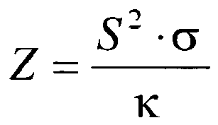
- The product S 2 ·σ ( is referred to as the power factor and serves for comparison of the thermoelectric materials.
- In addition, the dimensionless product Z •T is often also reported for comparative purposes. Thermoelectric materials known hitherto have maximum values of Z •T of about 1 at an optimal temperature. Beyond this optimal temperature, the values of Z •T are often significantly lower than 1.
- A more precise analysis shows that the efficiency ( is calculated from


- The aim is thus to provide a thermoelectric material having a maximum value of Z and a high realizable temperature differential. From the point of view of solid state physics, many problems have to be overcome here:
- A high σ requires a high electron mobility in the material, i.e. electrons (or holes in p-conducting materials) must not be bound strongly to the atomic cores. Materials having high electrical conductivity σ usually also have a high thermal conductivity (Wiedemann - Franz law), which does not allow Z to be favourably influenced. Materials used at present, such as Bi2Te3, already constitute compromises. For instance, the electrical conductivity is lowered to a lesser extent by alloying than the thermal conductivity. Preference is therefore given to using alloys, for example (Bi2Te3)90(Sb2Te3)5(Sb2Se3)5 or Bi12Sb23Te65.
- For thermoelectric materials having high efficiency, still further boundary conditions preferably have to be fulfilled. For instance, they have to be sufficiently thermally stable to be able to work under operating conditions over the course of years without significant loss of efficiency. This requires a phase which is thermally stable at high temperatures per se, a stable phase composition, and negligible diffusion of alloy constituents into the adjoining contact materials.
- For the production of a thermoelectric module, n- and p-conductors are always necessary. In order to arrive at a maximum efficiency of the module, i.e. at a maximum cooling performance in the case of a Peltier arrangement or a maximum generator performance in the case of a Seebeck arrangement, p-conductive and n-conductive material must be as well matched to one another as possible. This relates in particular to the parameters of Seebeck coefficient (ideally S(n) = -S(p)), electrical conductivity (ideally σ(n) = σ(p)), thermal conductivity (ideally λ(n) = λ(p)) and coefficient of thermal expansion (ideally α(n) = α(p)).
- In a thermoelectric module the metals/semiconductor materials are joined together by electrodes (for transportation of the generated current) and electrically isolated from other external parts. The electrodes are contacted with an electrical insulator material which should allow for a good heat flow from a heat source to the thermoelectric material. Therefore, thin insulator material layers are necessary and an excellent contacting interface has to be achieved.
- Typically, thermoelectric modules incorporate ceramic plates, made for example of SiO2, Al2O3 or AIN as supports having electrical insulating properties in order to prevent short-circuiting of the generated voltages. Crucially for a good heat flow from the heat source to the thermoelectric materials is a good thermally conductive substrate and an excellent joining of the parts for a minimal heat loss. Additionally, several applications, for example applications with mobile or vibrating parts, require also good mechanical stability of the substrates.
-
US 2008/0271771 relates to a thermoelectric conversion module which includes a good thermally conductive substrate consisting of aluminum or aluminum alloy having an anode oxide film in order to ensure the electrical insulation. The anode oxidation is an oxidative reaction that occurs on the anode upon the electrolysis, and the anode oxide film of Al2O3 is formed on a surface of the aluminum or the aluminum alloy by electrolysing the aluminum or the aluminum alloy in an electrolytic solution such as sulphuric acid. - It has been found that oxide films as disclosed in the US-reference are unreliable for preventing short circuits. Also, for high temperature application like heat recovery from exhaust gas, melting beds, motors, the temperature of the source can be as high as 600°C, and owing to the low melting point of 663°C, aluminum supports cannot be used safely.
-
US 2002/0162338 relates to a laser module, Peltier module or an Peltier module integrated heat spreader. The thermoelectric module described contains metal substrates on which an insulating thin film is formed which lies between the contacts connecting the thermoelectric legs and the substrates. The insulating thin films can be a ceramic thin film, for example of SiO2, Al2O3, AIN, MgO, or a non-conductive organic material. The insulating thin film can be formed on the surface of the metal substrates by highfrequency pump type ion plating, see page 3, paragraph [0034] and [0035]. According to example 1 the electrical insulating film of Al2O3 is deposited by means of vacuum deposition, see page 6, paragraph [0070]. -
US 2007/0028955 relates to a thermoelectric device and method of manufacturing the same. The thermoelectric device has a metal substrate and thermoelectric elements, wherein an insulating layer is provided between the substrates and the thermoelectric legs. The insulating layer is preferably a resin or a resin containing ceramic powder. For example an epoxy resin containing the ceramic powder is employed as the insulating layer, see page 4, paragraph [0073]. - The object of the present invention is to provide a thermoelectric module having an improved electrical insulating material on the substrate. Preferably, the substrate should have a higher heat resistance than aluminum.
- The object is achieved according to the present invention by a thermoelectric module comprising a series of p and n type semiconductors connected in series by conductive contacts, the conductive contacts being in contact with a substrate of moderate to high thermal conductivity that is electrically insulated from the conductive contacts by a resistive surface layer comprising a ceramic material, wherein the resistive surface layer is formed by a coating of a mixture of glass and ceramic material having a ratio of from 5 to 95 % by weight of ceramic material to 95 to 5 % by weight of glass.
- The conductive contacts can e. g. be supported on the substrate or on the semiconduc-tors/thermoelectric material.
- The object is furthermore achieved by a process for preparing a thermoelectric module as defined above, involving the step of applying the resistant surface layer to the substrate by electrophoretic deposition.
- The object is furthermore achieved by the use of the above thermoelectric module for use as a heat pump, for climate control of seating furniture, vehicles and buildings, in refrigerators and (laundry) driers, for simultaneous heating and cooling of streams in processes for substance separation, as a generator for utilizing heat sources or for cooling electronic components.
- The object is furthermore achieved by a heat pump, cooler, refrigerator, (laundry) drier, generator for utilizing heat sources, generator for converting thermal energy to electrical energy, comprising at least one thermoelectric module as defined above.
- According to the present invention it was found that ceramic materials form good and secure thin electrically insulating barrier layers on substrates with a coverage over the entire surface of the module. The thermoelectric module according to the present invention has suitable strength properties, is stable at a continuous operational temperature up to 600°C and shows good thermal conductivity as well as good electrical resistance.
- The resistive surface layer is formed by a coating of a mixture of glass and ceramic material. The ceramic material can be chosen from a wide variety of ceramic materials which have good insulating properties. Preferably, the ceramic material comprises alumina, zirconia or mixtures thereof. The ceramic material is employed as a mixture with glass, having a ratio of from 5 to 95% by weight of ceramic material to 95 to 5% by weight of glass, preferably 10 to 90% by weight of ceramic material and 90 to 10% by weight of glass, specifically 20 to 80% by weight of ceramic material and 80 to 20% by weight of glass.
- The substrate is preferably a metal or a metal alloy, a semimetal, a semiconductor, graphite, electrically conductive ceramics or combinations thereof, preferably a metal or a metal alloy. More preferably, the substrate is a heat resistant steel, iron or nickel alloy. Preferred metal substrates include FeCralloy, Crofer ferritic steel, nickel-plated steel and NiCr-alloys, for example as available under Inconel®. Further metal substrates, which preferably have a higher thermal stability than aluminum or aluminum alloys, are also suited according to the present invention.
- The geometric form of the substrate can be chosen from any suitable desired form required by the application. There are no restrictions as to the form of the substrate. Preferably, the metal substrates are flat metal substrates like foils or sheets or derived therefrom by shaping.
- It is possible to form a thermoelectric device in which the substrate is formed directly on the hot surface of a body from which it is desired to recover waste heat, for example from the surface of an engine or exhaust pipes. E. g. sheets of the metal substrate can be brought into cylindrical form for inserting in or forming part of an exhaust pipe.
- The substrate can haven an unrestricted three-dimensional geometric form which preferably can be obtained by forming a substrate sheet. Thus, the thickness is small with regard to the other dimensions like in sheets, plates, cylinders, circles, etc.
- The thickness of the resistive surface layer on the substrate is preferably in the range of from 1 µm to 500 µm, more preferably of from 1 to 100 µm, specifically of from 15 to 35 µm.
- The conductive contacts of the thermoelectric module can be deposited on or applied onto the electrically isolated substrate or they can be deposited on or applied onto the thermoelectric material.
- The thermoelectric design according to the present invention allows for the integration of the electrodes on the coated electrically insulated metal substrate. Electrodes can be prepared by several deposition methods, for example lithography, spray, paint, printing, dipping. The specific resistive surface allows for a very uniform electrode having a thickness as desired. High quality electrodes with thicknesses in the range of from 100 nm to 1 mm electrode can be achieved according to the present invention.
- Furthermore, according to the present invention, it is possible to embed, clamp or insert the thermoelectric materials in a solid matrix, wherein the matrix material has a low thermal and electrical conductivity and preferably is a ceramic, glass, mica, aerogel or a combination of these materials. The matrix protects the thermoelectric system (materials and contacts) from degradation and contamination due to external factors like humidity, oxygen or chemicals.
- This matrix can be clamped or inserted between the two isolated metal substrates. The electrodes can be applied either on the isolated substrate or on the thermoelectric materials. The matrix consists of a material or material mixture with low thermal conductivity, so that the heat flows through the thermoelectric material and not through the matrix. While the above materials are preferred, any non-conductive material with low thermal conductivity may be employed.
- The resistive surface layer can be applied to the substrate by all suitable processes. Preferably, the resistive surface layer is applied to the substrate by electrophoretic deposition.
- Electrophoretic deposition (EPD) is a term which in context with the invention includes electrocoating, electroplating cathodic electrodeposition, and electrophoretic coating, or electrophoretic painting. A characteristic feature of this process is that colloidal parti-cles suspended in a liquid medium migrate under the influence of an electric field (electrophoresis) and are deposited onto an electrode. All colloidal particles that can form ceramic coating or ceramic containing coatings and can be used to form stable suspensions and that can carry a charge can be used in electrophoretic deposition. This includes material classes such as ceramics and ceramics/glass mixtures.
- The process is useful for applying materials to any electrically conductive surface. The materials which are being deposited are the major determining factor in the actual processing conditions and equipment which may be used.
- Due to the wide utilization of electrophoretic painting processes in many industries, aqueous EPD is the most common commercially used EPD process. However, non-aqueous electrophoretic deposition applications are known. Applications of non-aqueous EPD are used in the fabrication of electronic components and the production of ceramic coatings. Non-aqueous processes have the advantage of avoiding the electrolysis of water and the gas evolution which accompanies electrolysis.
- This process is industrially used for applying coatings to metal fabricated products. It has been widely used to coat automobile bodies and parts, tractors and heavy equipment, electrical switch gear, appliances, metal furniture, beverage containers, fasteners, and many other industrial products.
- This process has a number of advantages which have made it widely used
- 1. The process applies coatings which generally have a very uniform coating thickness without porosity.
- 2. Complex fabricated objects can easily be coated, both inside cavities as well as on the outside surfaces.
- 3. Relatively high speed of coating.
- 4. Relatively high purity.
- 5. Applicability to wide range of materials (e.g. ceramics, glass etc.)
- 6. Easy control of the coating composition.
- 7. The process is normally automated and requires less human labor than other coating processes.
- 8. Highly efficient utilization of the coating materials result in lower costs relative to other processes.
- 9. The aqueous process which is commonly used has less risk of fire relative to the solvent-borne coatings that they have replaced.
- The overall industrial process of electrophoretic deposition consists of several sub-processes:
- 1. The object to be coated needs to be prepared for coating. This normally consists of some kind of cleaning process and may include the application of a conversion coating, typically an inorganic phosphate coating.
- 2. The coating process itself normally involves submerging the part into a container or vessel which holds the coating bath or solution and applying direct current electricity through the EPD bath using electrodes. Typically voltages of 25 - 400 volts DC are used in electrocoating or electrophoretic painting applications. The object to be coated is one of the electrodes, and a set of "counter-electrodes" are used to complete the circuit.
- 3. After deposition, the object is normally rinsed to remove the undeposited bath.
The rinsing process may utilize an ultrafilter to dewater a portion of the bath from the coating vessel to be used as rinse material. If an ultrafilter is used, all of the rinsed off materials can be returned to the coating vessel, allowing for high utilization efficiency of the coating materials, as well as reducing the amount of waste discharged into the environment. - 4. A baking or sintering process is normally used following the rinse. This will allow the coating, which might be porous due to the evolution of gas during the deposition process, to become smooth and continuous.
- There are two types of EPD processes, anodic and cathodic. In the anodic process, negatively charged material is deposited on the positively charged electrode, or anode. In the cathodic process, positively charged material is deposited on the negatively charged electrode, or cathode.
- When an electric field is applied, all of the charged species migrate by the process of electrophoresis towards the electrode with the opposite charge. There are several mechanisms by which material can be deposited on the electrode.
- The deposited coating has significantly higher resistance than the object which is being coated. As the deposited film precipitates, the resistance increases. The increase in resistance is proportional to the thickness of the deposited film, and thus, at a given voltage, the electric current decreases as the film gets thicker until it finally reaches a point where deposition has slowed or stopped occurring (self limiting). Thus the applied voltage is the primary control for the amount of film applied.
- The coating temperature is also variable affecting the EPD process. The coating temperature has an effect on the bath conductivity and deposited film conductivity, which increases as temperature increases. Temperature also has an effect on the viscosity of the deposited film, which in turn affects the ability of the deposited film to release any gas bubbles being formed.
- In the deposition of ceramic materials, voltages above 3-4V should not be applied in aqueous EPD if it is necessary to avoid the electrolysis of water. However, higher application voltages may be desirable in order to achieve higher coating thicknesses or to increase the rate of deposition. In such applications, organic solvents are used instead of water as the liquid medium. The organic solvents used are generally polar solvents such as alcohols and ketones. Ethanol, acetone, and methyl ethyl ketone are examples of solvents which are suitable candidates for use in electrophoretic deposition.
- In the electrophoretic process according to the present invention, the ceramic material preferably comprises alumina, zirconia, titania, silica, boron oxide or mixtures thereof. Further additives or elements like Ba, Sr, Na, Li, K, Pb, Ta, Hf, W, Mo, Cr, Ir, La, In, Ga, typically their oxides, may be present.
- The electrophoretic deposition is optionally followed by isostatic pressing followed by sintering to near theoretical density in order to achieve good mechanical stability and good electrical insulation of the metal plates.
- Sintering is preferably performed at a temperature in the range of from 650 to 1400 °C in an atmosphere of air or inert gas, especially nitrogen.
- As the thermoelectric material, all thermoelectric materials may be employed according to the present invention. Typical thermoelectric materials are e.g. disclosed in
US 5,448,109 ,WO 2007/104601 ,WO 2007/104603 . Pb tellurides are preferred. - The materials are generally produced by reactive grinding or preferably by co-melting and reaction of mixtures of the particular elemental constituents or alloys thereof. In general, a reaction time for the reactive grinding or preferably co-melting of at least one hour has been found to be advantageous.
- The thermoelectric materials are prepared generally in an evacuated and sealed quartz tube. Mixing of the components involved can be ensured by use of a rotatable and/or tiltable oven. On completion of the reaction, the oven is cooled. Thereafter, the quartz tube is removed from the oven and the semiconductor material present in the form of blocks is cut into slices. These slices are then cut into pieces of length about 1 to 5 mm, from which thermoelectric modules can be manufactured.
- Instead of a quartz tube, it is also possible to use tubes or ampules of other materials which are inert with respect to the semiconductor material, for example of tantalum.
- Instead of tubes, it is also possible to use other vessels of a suitable shape. It is also possible to use other materials, for example graphite, as the vessel material, provided that they are inert with respect to the semiconductor material. The materials can also be synthesized by melting/co-melting in an induction oven, for example in graphite ceramic or quartz crucibles.
- This gives rise to a process which comprises the following process steps:
- (1) co-melting mixtures of the particular elemental constituents or alloys thereof with the at least quaternary or ternary compound;
- (2) grinding the material obtained in process step (1);
- (3) pressing or extruding the material obtained in process step (2) to moldings
and - (4) optionally sintering the moldings obtained in process step (3).
- The semiconductor materials can be combined to form thermoelectric generators or Peltier arrangements by methods which are known per se to the person skilled in the art and are described, for example, in
WO 98/44562 US 5,448,109 ,EP-A-1 102 334 orUS 5,439,528 . - By varying the chemical composition of the thermoelectric generators or Peltier arrangements, it is possible to provide different systems which satisfy different requirements in a multitude of possible applications. The inventive thermoelectric generators or Peltier arrangements thus widen the range of application of these systems.
- The present invention also relates to the use of an inventive thermoelectric module
- as a heat pump
- for climate control of seating furniture, vehicles and buildings
- in refrigerators and (laundry) driers
- for simultaneous heating and cooling of streams in processes for substance separation such as
- absorption
- drying
- crystallization
- evaporation
- distillation
- as a generator for utilization of heat sources such as
- solar energy
- geothermal heat
- heat of combustion of fossil fuels
- waste heat sources in vehicles and stationary units
- heat sinks in the evaporation of liquid substances
- biological heat sources
- for cooling electronic components.
- as a generator for converting thermal energy to electrical energy, for example in motor vehicles, heating systems or power plants
- The present invention further relates to a heat pump, to a cooler, to a refrigerator, to a (laundry) drier, to a generator for converting thermal energy to electrical energy or to a generator for utilizing heat sources, comprising at least one inventive thermoelectric module.
- The present invention is illustrated in detail with reference to the examples described below.
- The powder materials were an yttria partially-stabilized zirconium oxide from MEL Chemicals, and aluminium oxide from Sumitomo Chemical Company. Suspensions of the materials in amyl alcohol were vibro-energy milled to a particle size distribution with a mean of 0.2 µm. EPD was carried out on cathodes consisting of 60 mm x 60 mm metallic foil substrates supported around the 4 edges so that the deposition area was 44 mm x 44 mm. The deposition potential was 30 V. To avoid problems of drying cracks due to shrinkage of the deposited film a 3-step process was used.
- At each step deposition was carried out for approximately 2 minutes and the coated substrate was then removed from the bath and allowed to dry. This process was repeated so that the total deposition time was approximately 6 minutes.
- Coatings of good visual appearance were processed further by isostatic pressing followed by sintering to near theoretical density at various temperatures for 1 hour. The coating thickness was determined from measurements of the deposit weight and area, assuming a theoretical density of 3.965 g/cm3 for alumina and 5.89 g/cm3 for zirconia. The coating thickness was approximately 20 µm for zirconia and 30 µm for alumina as shown in tables 1 and 2.
- Coated, electrically isolating metal plates were used for electrode deposition. Platinum-gold paint was applied by brush coating to areas of selected samples, after masking the coating. The platinum-gold coating was fired at 800 °C for 30 minutes. Samples labelled X in tables 1 and 2 were evaluated for electrical resistance. The insulting effect of the coating was tested as described below:
- The coated test piece was clamped between two stainless steel plates electrically isolated from each other. The pressing force was 2 N/mm2 in the pressed area. Using an external voltage source, a voltage of 15 V was laid on the two steel plates and the electrical current was measured. The minimal detection limit of the current was 0.010 mA.
Table 1 Zirconia coatings No. Metal substrate Coating thickness (µum) Sintering T °C/Atmosphere Ceramic coating resistance 10 Fecralloy 18.3 1300 air infinitely 11 Ferritic steel 18.7 1300 N2 12 Ni-plated steel 20.0 None 13 Inconel 20.0 None 14* Fecralloy 21.2 1325 air 0.75 MOhm 15* Fecralloy 21.5 1325 air 16 Fecralloy 21.0 None 17* Fecralloy 20.8 1300 air 18 Fecralloy 20.8 1325 air infinitely Table 2 Alumina coatings No. Metal substrate Coating thickness (µm) Sintering T °C/Atmosphere Ceramic coating resistance 19* Fecralloy 28.0 1325 air 20* Ferritic steel 28.5 1300 N2 infinitely 21 Ni-plated steel 26.6 1325 Ar/H2 22 Inconel 26.3 1325 Ar/H2 23* Fecralloy 28.7 1325 air 24 Fecralloy 30.2 1325 air infinitely 25 Fecralloy 29.3 1325 air infinitely 26 Fecralloy 28.4 1325 air - A composite glass-ceramic powder suspension suitable for EPD was produced by grinding the glass to a powder, mixing with the Sumitomo alumina powder and dispersing in alcohol. The glass used in this composite was an aluminoborate glass with the composition 46% SiO2, 25% B2O3, 10% Al2O3, 4% Na2O, 3% CaO, 6% SrO and 6% BaO. Trials were carried out to form a composite coating of 80% glass to 20% alumina by weight on Fecralloy foil by EPD with a deposition time of approximately 1 minute. The coating was uniform, adherent, free of texture and free of porosity or microcracks. The thickness of the glass/alumina coating was 7 µm. Further EPD trials showed that it was possible to produce glass coatings up to 30 µm thickness on Fecralloy, but owing to the low thermal conductivity of glass a thin coating is preferred for the thermoelectric application.
- Coatings containing other proportions of glass to alumina ranging from 100% glass to 100% alumina are possible by this method. However, because of the low thermal conductivity of glass (1 W/mK) compared to alumina (30 W/mK) a high proportion of glass is not desirable for thermoelectric application. On the other hand a composition with a higher glass content is easier to process, which allows the possibility of fabricating a thinner coating without the risk of pinholes or short-circuiting. Possible embodiments of this aspect of the invention are shown in Table 3.
Table 3 Possible glass: alumina coatings % glass % alumina Thickness (µm) 0 100 30 20 80 20 40 60 10 80 20 5 - Samples of uncoated Fecralloy, both foils and 1 mm thick plates, were heat treated in air at 1100 °C for 2 hours to develop an insulating layer of α-Al2O3 formed by thermal oxidation of the alloy. The thickness of the layer was in the range 0.5 to 0.6 µm. These surface oxide films showed evidence of poor electrical insulation in a test wing pointed electrical contacts.
- Samples of uncoated Fecralloy, both foils and 1 mm thick plates, were heat treated at 1100 °C for 2 hours in steam. This thermal treatment resulted in an insulating layer of α-Al2O3 formed by steam oxidation of the alloy. The thickness of the layer was in the range 1.5 to 2 µm. The result of the resistance measurement test shown that this coatings are not sufficiently isolating (at 0.37 mV was measured a current of 2 A).
Claims (12)
- A thermoelectric module comprising a series of p and n type semiconductors connected in series by conductive contacts, the conductive contacts being in contact with a substrate of moderate to high thermal conductivity that is electrically insulated from the conductive contacts by a resistive surface layer comprising a ceramic material, characterized in that the resistive surface layer is formed by a coating of a mixture of glass and ceramic material having a ratio of from 5 to 95% by weight of ceramic material to 95 to 5% by weight of glass.
- The thermoelectric module according to claim 1, wherein the substrate is a metal, a metal alloy, a semimetal, a semi-conductor, graphite, electrically conductive ceramics or combinations thereof.
- The thermoelectric module according to any of claims 1 or 2, wherein the thickness of the resistive surface layer is in the range of from 1 µm to 500 µm, preferably of from 1 µm to 100 µm.
- The thermoelectric module according to any of claims 1 to 3, wherein the conductive contacts are deposited on the electrically insulated substrate.
- The thermoelectric module according to any of claims 1 to 3, wherein the conductive contacts are applied onto the thermoelectric materials.
- The thermoelectric module according to any of claims 1 to 5, wherein the thermoelectric materials are embedded, clamped or inserted in a solid matrix, wherein the matrix material has a low thermal and electrical conductivity and preferably is a ceramic, glass, mica, aerogel or a combination of these materials.
- The thermoelectric module according to any of claims 1 to 6, wherein the substrate is a heat resistant steel, iron or nickel alloy.
- The thermoelectric module according to any of claims 1 to 7, wherein the ceramic material comprises alumina, zirconia, titania, silica, boron oxide or mixtures thereof.
- The thermoelectric module according to any of claims 1 to 8, wherein the substrate has an unrestricted three-dimensional geometrical form which preferably can be obtained by forming a substrate sheet.
- A process for preparing a thermoelectric material according to any of claims 1 to 9, involving the step of applying the resistive surface layer to the substrate by electrophoretic deposition.
- The use of a thermoelectric module according to any of claims 1 to 9 for use as a heat pump, for climate control of seating furniture, vehicles and buildings, in refrigerators and (laundry) driers, for simultaneous heating and cooling of streams in processes for substance separation, as a generator for utilizing heat sources or for cooling electronic components.
- A heat pump, cooler, refrigerator, (laundry) drier, generator for utilizing heat sources, generator for converting thermal energy to electrical energy, comprising at least one thermoelectric module according to any of claims 1 to 9.
Priority Applications (1)
| Application Number | Priority Date | Filing Date | Title |
|---|---|---|---|
| EP10711894.5A EP2415090B1 (en) | 2009-04-02 | 2010-03-31 | Thermoelectric module with insulated substrate |
Applications Claiming Priority (3)
| Application Number | Priority Date | Filing Date | Title |
|---|---|---|---|
| EP09157158 | 2009-04-02 | ||
| EP10711894.5A EP2415090B1 (en) | 2009-04-02 | 2010-03-31 | Thermoelectric module with insulated substrate |
| PCT/EP2010/054268 WO2010115792A1 (en) | 2009-04-02 | 2010-03-31 | Thermoelectric module with insulated substrate |
Publications (2)
| Publication Number | Publication Date |
|---|---|
| EP2415090A1 EP2415090A1 (en) | 2012-02-08 |
| EP2415090B1 true EP2415090B1 (en) | 2013-10-23 |
Family
ID=42357317
Family Applications (1)
| Application Number | Title | Priority Date | Filing Date |
|---|---|---|---|
| EP10711894.5A Not-in-force EP2415090B1 (en) | 2009-04-02 | 2010-03-31 | Thermoelectric module with insulated substrate |
Country Status (10)
| Country | Link |
|---|---|
| US (1) | US20120017963A1 (en) |
| EP (1) | EP2415090B1 (en) |
| JP (1) | JP2012523111A (en) |
| KR (1) | KR20120007027A (en) |
| CN (1) | CN102449791A (en) |
| CA (1) | CA2757530A1 (en) |
| RU (1) | RU2011144115A (en) |
| SG (1) | SG174559A1 (en) |
| TW (1) | TW201042788A (en) |
| WO (1) | WO2010115792A1 (en) |
Families Citing this family (11)
| Publication number | Priority date | Publication date | Assignee | Title |
|---|---|---|---|---|
| CN102414121A (en) * | 2009-03-24 | 2012-04-11 | 巴斯夫欧洲公司 | Self-Assembled Thermoelectric Materials |
| US9082928B2 (en) | 2010-12-09 | 2015-07-14 | Brian Isaac Ashkenazi | Next generation thermoelectric device designs and methods of using same |
| JP2013026334A (en) * | 2011-07-19 | 2013-02-04 | National Institute Of Advanced Industrial & Technology | Stacked thermoelectric conversion module |
| US10454013B2 (en) * | 2012-11-16 | 2019-10-22 | Micropower Global Limited | Thermoelectric device |
| US9276190B2 (en) | 2013-10-01 | 2016-03-01 | The Pen | Practical method of producing an aerogel composite continuous thin film thermoelectric semiconductor material by modified MOCVD |
| US9040339B2 (en) | 2013-10-01 | 2015-05-26 | The Pen | Practical method of producing an aerogel composite continuous thin film thermoelectric semiconductor material |
| CN105207529A (en) * | 2015-10-28 | 2015-12-30 | 蒋安为 | Infrared light power generation device |
| NO341705B1 (en) * | 2016-02-22 | 2018-01-02 | Tegma As | Thermoelectric half-cell and method of production |
| CN107124108A (en) * | 2016-02-25 | 2017-09-01 | 西门子公司 | Thermal management method, device and the equipment for including high-power heater element |
| KR102050138B1 (en) * | 2017-12-07 | 2019-11-28 | 한국세라믹기술원 | Multilayered substrate of electrode layer/insulation layer, manufacturing method thereof,and thermoelectric generator module comprising the same |
| DE102019207227B4 (en) * | 2019-05-17 | 2021-10-07 | Fraunhofer-Gesellschaft zur Förderung der angewandten Forschung e.V. | Process for the production of thermoelectric elements with electrical connection contacts as well as a thermoelectric module produced with the process |
Family Cites Families (25)
| Publication number | Priority date | Publication date | Assignee | Title |
|---|---|---|---|---|
| US4794048A (en) * | 1987-05-04 | 1988-12-27 | Allied-Signal Inc. | Ceramic coated metal substrates for electronic applications |
| US5209786A (en) * | 1990-10-09 | 1993-05-11 | Thermo Electron Technologies Corporation | Integrity-enhanced thermoelectrics |
| US5439528A (en) | 1992-12-11 | 1995-08-08 | Miller; Joel | Laminated thermo element |
| US5448109B1 (en) | 1994-03-08 | 1997-10-07 | Tellurex Corp | Thermoelectric module |
| JPH09139525A (en) * | 1995-11-15 | 1997-05-27 | Hitachi Chem Co Ltd | Peltier cooling unit structure |
| WO1998044562A1 (en) | 1997-03-31 | 1998-10-08 | Research Triangle Institute | Thin-film thermoelectric device and fabrication method of same |
| JP2000164941A (en) * | 1998-11-30 | 2000-06-16 | Yamaha Corp | Thermoelectric conversion module |
| JP2000286467A (en) * | 1999-03-31 | 2000-10-13 | Nhk Spring Co Ltd | Electrical insulating material, module and method of manufacturing the same |
| JP3163380B2 (en) * | 1999-08-05 | 2001-05-08 | 科学技術庁航空宇宙技術研究所長 | Electrical insulation and manufacturing method thereof |
| DE19955788A1 (en) | 1999-11-19 | 2001-05-23 | Basf Ag | Thermoelectrically active materials and generators containing them |
| JP3680684B2 (en) * | 2000-03-06 | 2005-08-10 | 株式会社村田製作所 | Insulator porcelain, ceramic multilayer substrate, ceramic electronic component and multilayer ceramic electronic component |
| JP2002280621A (en) * | 2001-01-15 | 2002-09-27 | Furukawa Electric Co Ltd:The | Laser module, Peltier module and Peltier module integrated heat spreader |
| US6826916B2 (en) * | 2001-04-24 | 2004-12-07 | The Furukawa Electric Co., Ltd. | Laser module, Peltier module, and Peltier module integrated heat spreader |
| JP2003174202A (en) * | 2001-09-25 | 2003-06-20 | Sumitomo Electric Ind Ltd | Thermoelectric device, optical module using the same, and methods of manufacturing these |
| JP2005033095A (en) * | 2003-07-10 | 2005-02-03 | Hitachi Powdered Metals Co Ltd | Method for manufacturing thermal stress relaxation pad for thermoelectric converter |
| CN1969398A (en) * | 2004-06-17 | 2007-05-23 | 阿鲁策株式会社 | Thermoelectric conversion module |
| JP2006066822A (en) * | 2004-08-30 | 2006-03-09 | Denso Corp | Thermoelectric converter |
| FR2882371B1 (en) * | 2005-02-24 | 2008-01-18 | Centre Nat Rech Scient | COMPOSITE MATERIAL CONSISTING OF A POROUS MATRIX AND NANOPARTICLES OF METAL OR METAL OXIDE |
| CN1304327C (en) * | 2005-06-22 | 2007-03-14 | 中国科学院上海硅酸盐研究所 | Method for promoting insulation electrical resistivity of titanium containing microwave medium ceramic buring with copper |
| CN100579929C (en) * | 2005-07-19 | 2010-01-13 | 宁波材料技术与工程研究所 | Preparation method of nanocomposite low melting point glass insulating coating |
| JP2007035907A (en) * | 2005-07-27 | 2007-02-08 | Kyocera Corp | Thermoelectric module |
| CN100585896C (en) * | 2005-08-02 | 2010-01-27 | 株式会社东芝 | Thermoelectric device and method for manufacturing the same |
| JP4901350B2 (en) * | 2005-08-02 | 2012-03-21 | 株式会社東芝 | Thermoelectric conversion device and manufacturing method thereof |
| WO2007104603A2 (en) | 2006-03-16 | 2007-09-20 | Basf Se | Lead-germanium-tellurides for thermoelectrical applications |
| UA92213C2 (en) | 2006-03-16 | 2010-10-11 | Басф Се | SEMICONDUCTOR MATERIAL FOR THERMOELECTRIC APPLICATION AND THERMOELECTRIC GENERATOR CONTAINING IT |
-
2010
- 2010-03-31 JP JP2012502658A patent/JP2012523111A/en active Pending
- 2010-03-31 SG SG2011069424A patent/SG174559A1/en unknown
- 2010-03-31 KR KR1020117026168A patent/KR20120007027A/en not_active Withdrawn
- 2010-03-31 CN CN2010800237638A patent/CN102449791A/en active Pending
- 2010-03-31 RU RU2011144115/28A patent/RU2011144115A/en not_active Application Discontinuation
- 2010-03-31 WO PCT/EP2010/054268 patent/WO2010115792A1/en not_active Ceased
- 2010-03-31 CA CA2757530A patent/CA2757530A1/en not_active Abandoned
- 2010-03-31 US US13/259,872 patent/US20120017963A1/en not_active Abandoned
- 2010-03-31 EP EP10711894.5A patent/EP2415090B1/en not_active Not-in-force
- 2010-04-02 TW TW099110431A patent/TW201042788A/en unknown
Also Published As
| Publication number | Publication date |
|---|---|
| EP2415090A1 (en) | 2012-02-08 |
| WO2010115792A1 (en) | 2010-10-14 |
| RU2011144115A (en) | 2013-05-10 |
| CA2757530A1 (en) | 2010-10-14 |
| CN102449791A (en) | 2012-05-09 |
| US20120017963A1 (en) | 2012-01-26 |
| TW201042788A (en) | 2010-12-01 |
| SG174559A1 (en) | 2011-10-28 |
| KR20120007027A (en) | 2012-01-19 |
| JP2012523111A (en) | 2012-09-27 |
Similar Documents
| Publication | Publication Date | Title |
|---|---|---|
| US20120017963A1 (en) | Thermoelectric module with insulated substrate | |
| EP2415089B1 (en) | Thermoelectric material coated with a protective layer | |
| Gu et al. | A high-throughput strategy to screen interfacial diffusion barrier materials for thermoelectric modules | |
| EP2461383B1 (en) | Magnesium-silicon composite material and process for producing same, and thermoelectric conversion material, thermoelectric conversion element, and thermoelectric conversion module each comprising or including the composite material | |
| EP2913857B1 (en) | Mg-Si THERMOELECTRIC CONVERSION MATERIAL, METHOD FOR PRODUCING SAME, SINTERED BODY FOR THERMOELECTRIC CONVERSION, THERMOELECTRIC CONVERSION ELEMENT, AND THERMOELECTRIC CONVERSION MODULE | |
| Antharam et al. | Milliwatt-scale 3D thermoelectric generators via additive screen printing | |
| CN104321889B (en) | Thermo-electric converting material and use its thermo-electric conversion module and its manufacture method | |
| TW201406976A (en) | A manufacturing method of thermoelectric conversion materials | |
| Norizuki et al. | Fabrication and characterization of ceramic-iron joint coating for electrical insulation | |
| Su et al. | Micro-thermoelectric devices with large output power fabricated on a multi-channel glass template | |
| Talebi et al. | Fabrication of n-type Bi2Te3 film using electrophoretic deposition for thermoelectric applications | |
| RU2570429C1 (en) | Thermoelectric module | |
| Schilm et al. | TiOx based thermoelectric modules–manufacturing, properties and operational behavior | |
| Talebi et al. | Suspension Characteristics and Electrophoretic Deposition of p-Type Bi2Te3 Films for Thermoelectric Applications | |
| Choi et al. | Fabrication of aluminum-based thermal radiation plate for thermoelectric module using aluminum anodic oxidization and copper electroplating | |
| CA2069101A1 (en) | Method of making nitride and oxide electrodes on a solid electrolyte | |
| Weil | High-temperature electrical testing of a solid oxide fuel cell cathode contact material | |
| JP5718671B2 (en) | Thermoelectric conversion material and manufacturing method thereof | |
| Naser et al. | Low-cost thermal evaporation instruments: Design, implementation, and evaluation | |
| Qiu et al. | Effect of hot-press treatment on electrochemically deposited antimony telluride film | |
| Martinez | Liquid metal thermal-electric converter electrode development | |
| Chu et al. | Performance evaluation of LSM-metallic interconnect composite films prepared by plasma sputtering method | |
| Wei et al. | Nickel/ceramic composites for current collection terminals | |
| JPS58170532A (en) | Vacuum heating apparatus | |
| Sarkar et al. | High Power Density Tubular SOFC for Portable Applications |
Legal Events
| Date | Code | Title | Description |
|---|---|---|---|
| PUAI | Public reference made under article 153(3) epc to a published international application that has entered the european phase |
Free format text: ORIGINAL CODE: 0009012 |
|
| 17P | Request for examination filed |
Effective date: 20111102 |
|
| AK | Designated contracting states |
Kind code of ref document: A1 Designated state(s): AT BE BG CH CY CZ DE DK EE ES FI FR GB GR HR HU IE IS IT LI LT LU LV MC MK MT NL NO PL PT RO SE SI SK SM TR |
|
| DAX | Request for extension of the european patent (deleted) | ||
| GRAP | Despatch of communication of intention to grant a patent |
Free format text: ORIGINAL CODE: EPIDOSNIGR1 |
|
| INTG | Intention to grant announced |
Effective date: 20130605 |
|
| GRAS | Grant fee paid |
Free format text: ORIGINAL CODE: EPIDOSNIGR3 |
|
| GRAA | (expected) grant |
Free format text: ORIGINAL CODE: 0009210 |
|
| AK | Designated contracting states |
Kind code of ref document: B1 Designated state(s): AT BE BG CH CY CZ DE DK EE ES FI FR GB GR HR HU IE IS IT LI LT LU LV MC MK MT NL NO PL PT RO SE SI SK SM TR |
|
| REG | Reference to a national code |
Ref country code: GB Ref legal event code: FG4D |
|
| REG | Reference to a national code |
Ref country code: CH Ref legal event code: EP |
|
| REG | Reference to a national code |
Ref country code: AT Ref legal event code: REF Ref document number: 637984 Country of ref document: AT Kind code of ref document: T Effective date: 20131115 |
|
| REG | Reference to a national code |
Ref country code: IE Ref legal event code: FG4D |
|
| REG | Reference to a national code |
Ref country code: DE Ref legal event code: R096 Ref document number: 602010011154 Country of ref document: DE Effective date: 20131219 |
|
| REG | Reference to a national code |
Ref country code: NL Ref legal event code: VDEP Effective date: 20131023 |
|
| REG | Reference to a national code |
Ref country code: AT Ref legal event code: MK05 Ref document number: 637984 Country of ref document: AT Kind code of ref document: T Effective date: 20131023 |
|
| REG | Reference to a national code |
Ref country code: LT Ref legal event code: MG4D |
|
| PG25 | Lapsed in a contracting state [announced via postgrant information from national office to epo] |
Ref country code: IS Free format text: LAPSE BECAUSE OF FAILURE TO SUBMIT A TRANSLATION OF THE DESCRIPTION OR TO PAY THE FEE WITHIN THE PRESCRIBED TIME-LIMIT Effective date: 20140223 Ref country code: SE Free format text: LAPSE BECAUSE OF FAILURE TO SUBMIT A TRANSLATION OF THE DESCRIPTION OR TO PAY THE FEE WITHIN THE PRESCRIBED TIME-LIMIT Effective date: 20131023 Ref country code: HR Free format text: LAPSE BECAUSE OF FAILURE TO SUBMIT A TRANSLATION OF THE DESCRIPTION OR TO PAY THE FEE WITHIN THE PRESCRIBED TIME-LIMIT Effective date: 20131023 Ref country code: BE Free format text: LAPSE BECAUSE OF FAILURE TO SUBMIT A TRANSLATION OF THE DESCRIPTION OR TO PAY THE FEE WITHIN THE PRESCRIBED TIME-LIMIT Effective date: 20131023 Ref country code: NO Free format text: LAPSE BECAUSE OF FAILURE TO SUBMIT A TRANSLATION OF THE DESCRIPTION OR TO PAY THE FEE WITHIN THE PRESCRIBED TIME-LIMIT Effective date: 20140123 Ref country code: NL Free format text: LAPSE BECAUSE OF FAILURE TO SUBMIT A TRANSLATION OF THE DESCRIPTION OR TO PAY THE FEE WITHIN THE PRESCRIBED TIME-LIMIT Effective date: 20131023 Ref country code: LT Free format text: LAPSE BECAUSE OF FAILURE TO SUBMIT A TRANSLATION OF THE DESCRIPTION OR TO PAY THE FEE WITHIN THE PRESCRIBED TIME-LIMIT Effective date: 20131023 Ref country code: FI Free format text: LAPSE BECAUSE OF FAILURE TO SUBMIT A TRANSLATION OF THE DESCRIPTION OR TO PAY THE FEE WITHIN THE PRESCRIBED TIME-LIMIT Effective date: 20131023 |
|
| PG25 | Lapsed in a contracting state [announced via postgrant information from national office to epo] |
Ref country code: CY Free format text: LAPSE BECAUSE OF FAILURE TO SUBMIT A TRANSLATION OF THE DESCRIPTION OR TO PAY THE FEE WITHIN THE PRESCRIBED TIME-LIMIT Effective date: 20131023 Ref country code: AT Free format text: LAPSE BECAUSE OF FAILURE TO SUBMIT A TRANSLATION OF THE DESCRIPTION OR TO PAY THE FEE WITHIN THE PRESCRIBED TIME-LIMIT Effective date: 20131023 Ref country code: LV Free format text: LAPSE BECAUSE OF FAILURE TO SUBMIT A TRANSLATION OF THE DESCRIPTION OR TO PAY THE FEE WITHIN THE PRESCRIBED TIME-LIMIT Effective date: 20131023 Ref country code: ES Free format text: LAPSE BECAUSE OF FAILURE TO SUBMIT A TRANSLATION OF THE DESCRIPTION OR TO PAY THE FEE WITHIN THE PRESCRIBED TIME-LIMIT Effective date: 20131023 |
|
| PG25 | Lapsed in a contracting state [announced via postgrant information from national office to epo] |
Ref country code: PT Free format text: LAPSE BECAUSE OF FAILURE TO SUBMIT A TRANSLATION OF THE DESCRIPTION OR TO PAY THE FEE WITHIN THE PRESCRIBED TIME-LIMIT Effective date: 20140224 |
|
| REG | Reference to a national code |
Ref country code: DE Ref legal event code: R097 Ref document number: 602010011154 Country of ref document: DE |
|
| PG25 | Lapsed in a contracting state [announced via postgrant information from national office to epo] |
Ref country code: EE Free format text: LAPSE BECAUSE OF FAILURE TO SUBMIT A TRANSLATION OF THE DESCRIPTION OR TO PAY THE FEE WITHIN THE PRESCRIBED TIME-LIMIT Effective date: 20131023 |
|
| PG25 | Lapsed in a contracting state [announced via postgrant information from national office to epo] |
Ref country code: SK Free format text: LAPSE BECAUSE OF FAILURE TO SUBMIT A TRANSLATION OF THE DESCRIPTION OR TO PAY THE FEE WITHIN THE PRESCRIBED TIME-LIMIT Effective date: 20131023 Ref country code: IT Free format text: LAPSE BECAUSE OF FAILURE TO SUBMIT A TRANSLATION OF THE DESCRIPTION OR TO PAY THE FEE WITHIN THE PRESCRIBED TIME-LIMIT Effective date: 20131023 Ref country code: PL Free format text: LAPSE BECAUSE OF FAILURE TO SUBMIT A TRANSLATION OF THE DESCRIPTION OR TO PAY THE FEE WITHIN THE PRESCRIBED TIME-LIMIT Effective date: 20131023 Ref country code: CZ Free format text: LAPSE BECAUSE OF FAILURE TO SUBMIT A TRANSLATION OF THE DESCRIPTION OR TO PAY THE FEE WITHIN THE PRESCRIBED TIME-LIMIT Effective date: 20131023 Ref country code: RO Free format text: LAPSE BECAUSE OF FAILURE TO SUBMIT A TRANSLATION OF THE DESCRIPTION OR TO PAY THE FEE WITHIN THE PRESCRIBED TIME-LIMIT Effective date: 20131023 |
|
| PLBE | No opposition filed within time limit |
Free format text: ORIGINAL CODE: 0009261 |
|
| STAA | Information on the status of an ep patent application or granted ep patent |
Free format text: STATUS: NO OPPOSITION FILED WITHIN TIME LIMIT |
|
| PG25 | Lapsed in a contracting state [announced via postgrant information from national office to epo] |
Ref country code: DK Free format text: LAPSE BECAUSE OF FAILURE TO SUBMIT A TRANSLATION OF THE DESCRIPTION OR TO PAY THE FEE WITHIN THE PRESCRIBED TIME-LIMIT Effective date: 20131023 |
|
| 26N | No opposition filed |
Effective date: 20140724 |
|
| PG25 | Lapsed in a contracting state [announced via postgrant information from national office to epo] |
Ref country code: LU Free format text: LAPSE BECAUSE OF FAILURE TO SUBMIT A TRANSLATION OF THE DESCRIPTION OR TO PAY THE FEE WITHIN THE PRESCRIBED TIME-LIMIT Effective date: 20140331 |
|
| REG | Reference to a national code |
Ref country code: CH Ref legal event code: PL |
|
| REG | Reference to a national code |
Ref country code: DE Ref legal event code: R097 Ref document number: 602010011154 Country of ref document: DE Effective date: 20140724 |
|
| GBPC | Gb: european patent ceased through non-payment of renewal fee |
Effective date: 20140331 |
|
| REG | Reference to a national code |
Ref country code: IE Ref legal event code: MM4A |
|
| PG25 | Lapsed in a contracting state [announced via postgrant information from national office to epo] |
Ref country code: CH Free format text: LAPSE BECAUSE OF NON-PAYMENT OF DUE FEES Effective date: 20140331 Ref country code: GB Free format text: LAPSE BECAUSE OF NON-PAYMENT OF DUE FEES Effective date: 20140331 Ref country code: IE Free format text: LAPSE BECAUSE OF NON-PAYMENT OF DUE FEES Effective date: 20140331 Ref country code: LI Free format text: LAPSE BECAUSE OF NON-PAYMENT OF DUE FEES Effective date: 20140331 |
|
| PG25 | Lapsed in a contracting state [announced via postgrant information from national office to epo] |
Ref country code: SI Free format text: LAPSE BECAUSE OF FAILURE TO SUBMIT A TRANSLATION OF THE DESCRIPTION OR TO PAY THE FEE WITHIN THE PRESCRIBED TIME-LIMIT Effective date: 20131023 |
|
| REG | Reference to a national code |
Ref country code: FR Ref legal event code: PLFP Year of fee payment: 6 |
|
| PGFP | Annual fee paid to national office [announced via postgrant information from national office to epo] |
Ref country code: DE Payment date: 20150601 Year of fee payment: 6 |
|
| PGFP | Annual fee paid to national office [announced via postgrant information from national office to epo] |
Ref country code: FR Payment date: 20150331 Year of fee payment: 6 |
|
| PG25 | Lapsed in a contracting state [announced via postgrant information from national office to epo] |
Ref country code: MT Free format text: LAPSE BECAUSE OF FAILURE TO SUBMIT A TRANSLATION OF THE DESCRIPTION OR TO PAY THE FEE WITHIN THE PRESCRIBED TIME-LIMIT Effective date: 20131023 |
|
| PG25 | Lapsed in a contracting state [announced via postgrant information from national office to epo] |
Ref country code: SM Free format text: LAPSE BECAUSE OF FAILURE TO SUBMIT A TRANSLATION OF THE DESCRIPTION OR TO PAY THE FEE WITHIN THE PRESCRIBED TIME-LIMIT Effective date: 20131023 |
|
| PG25 | Lapsed in a contracting state [announced via postgrant information from national office to epo] |
Ref country code: MC Free format text: LAPSE BECAUSE OF FAILURE TO SUBMIT A TRANSLATION OF THE DESCRIPTION OR TO PAY THE FEE WITHIN THE PRESCRIBED TIME-LIMIT Effective date: 20131023 |
|
| PG25 | Lapsed in a contracting state [announced via postgrant information from national office to epo] |
Ref country code: GR Free format text: LAPSE BECAUSE OF FAILURE TO SUBMIT A TRANSLATION OF THE DESCRIPTION OR TO PAY THE FEE WITHIN THE PRESCRIBED TIME-LIMIT Effective date: 20140124 Ref country code: BG Free format text: LAPSE BECAUSE OF FAILURE TO SUBMIT A TRANSLATION OF THE DESCRIPTION OR TO PAY THE FEE WITHIN THE PRESCRIBED TIME-LIMIT Effective date: 20131023 |
|
| PG25 | Lapsed in a contracting state [announced via postgrant information from national office to epo] |
Ref country code: TR Free format text: LAPSE BECAUSE OF FAILURE TO SUBMIT A TRANSLATION OF THE DESCRIPTION OR TO PAY THE FEE WITHIN THE PRESCRIBED TIME-LIMIT Effective date: 20131023 Ref country code: HU Free format text: LAPSE BECAUSE OF FAILURE TO SUBMIT A TRANSLATION OF THE DESCRIPTION OR TO PAY THE FEE WITHIN THE PRESCRIBED TIME-LIMIT; INVALID AB INITIO Effective date: 20100331 |
|
| REG | Reference to a national code |
Ref country code: DE Ref legal event code: R119 Ref document number: 602010011154 Country of ref document: DE |
|
| REG | Reference to a national code |
Ref country code: FR Ref legal event code: ST Effective date: 20161130 |
|
| PG25 | Lapsed in a contracting state [announced via postgrant information from national office to epo] |
Ref country code: FR Free format text: LAPSE BECAUSE OF NON-PAYMENT OF DUE FEES Effective date: 20160331 Ref country code: DE Free format text: LAPSE BECAUSE OF NON-PAYMENT OF DUE FEES Effective date: 20161001 |
|
| PG25 | Lapsed in a contracting state [announced via postgrant information from national office to epo] |
Ref country code: MK Free format text: LAPSE BECAUSE OF FAILURE TO SUBMIT A TRANSLATION OF THE DESCRIPTION OR TO PAY THE FEE WITHIN THE PRESCRIBED TIME-LIMIT Effective date: 20131023 |