EP2415085B1 - Optoelectronic semiconductor chip - Google Patents
Optoelectronic semiconductor chip Download PDFInfo
- Publication number
- EP2415085B1 EP2415085B1 EP10707304.1A EP10707304A EP2415085B1 EP 2415085 B1 EP2415085 B1 EP 2415085B1 EP 10707304 A EP10707304 A EP 10707304A EP 2415085 B1 EP2415085 B1 EP 2415085B1
- Authority
- EP
- European Patent Office
- Prior art keywords
- semiconductor chip
- quantum well
- zones
- indium content
- active quantum
- Prior art date
- Legal status (The legal status is an assumption and is not a legal conclusion. Google has not performed a legal analysis and makes no representation as to the accuracy of the status listed.)
- Active
Links
- 239000004065 semiconductor Substances 0.000 title claims description 106
- 230000005693 optoelectronics Effects 0.000 title claims description 49
- APFVFJFRJDLVQX-UHFFFAOYSA-N indium atom Chemical compound [In] APFVFJFRJDLVQX-UHFFFAOYSA-N 0.000 claims description 80
- 229910052738 indium Inorganic materials 0.000 claims description 79
- 230000004888 barrier function Effects 0.000 claims description 15
- 230000005855 radiation Effects 0.000 claims description 14
- 239000000463 material Substances 0.000 claims description 10
- 239000002800 charge carrier Substances 0.000 claims description 8
- 230000005670 electromagnetic radiation Effects 0.000 claims description 6
- 150000004767 nitrides Chemical class 0.000 claims description 4
- 230000004048 modification Effects 0.000 description 25
- 238000012986 modification Methods 0.000 description 25
- 229910052782 aluminium Inorganic materials 0.000 description 12
- XAGFODPZIPBFFR-UHFFFAOYSA-N aluminium Chemical compound [Al] XAGFODPZIPBFFR-UHFFFAOYSA-N 0.000 description 12
- 230000005428 wave function Effects 0.000 description 5
- 230000007423 decrease Effects 0.000 description 3
- 229910052757 nitrogen Inorganic materials 0.000 description 3
- IJGRMHOSHXDMSA-UHFFFAOYSA-N nitrogen Substances N#N IJGRMHOSHXDMSA-UHFFFAOYSA-N 0.000 description 3
- 230000003287 optical effect Effects 0.000 description 3
- 230000003595 spectral effect Effects 0.000 description 3
- 238000005253 cladding Methods 0.000 description 2
- 230000005283 ground state Effects 0.000 description 2
- 125000005842 heteroatom Chemical group 0.000 description 2
- 230000006798 recombination Effects 0.000 description 2
- 238000005215 recombination Methods 0.000 description 2
- 229910002704 AlGaN Inorganic materials 0.000 description 1
- 230000009471 action Effects 0.000 description 1
- 239000000969 carrier Substances 0.000 description 1
- 238000001493 electron microscopy Methods 0.000 description 1
- 238000005286 illumination Methods 0.000 description 1
- 238000004519 manufacturing process Methods 0.000 description 1
- QJGQUHMNIGDVPM-UHFFFAOYSA-N nitrogen group Chemical group [N] QJGQUHMNIGDVPM-UHFFFAOYSA-N 0.000 description 1
- 238000013139 quantization Methods 0.000 description 1
- 239000002096 quantum dot Substances 0.000 description 1
- 230000009467 reduction Effects 0.000 description 1
- 238000004627 transmission electron microscopy Methods 0.000 description 1
Images


Classifications
-
- H—ELECTRICITY
- H01—ELECTRIC ELEMENTS
- H01L—SEMICONDUCTOR DEVICES NOT COVERED BY CLASS H10
- H01L33/00—Semiconductor devices with at least one potential-jump barrier or surface barrier specially adapted for light emission; Processes or apparatus specially adapted for the manufacture or treatment thereof or of parts thereof; Details thereof
- H01L33/02—Semiconductor devices with at least one potential-jump barrier or surface barrier specially adapted for light emission; Processes or apparatus specially adapted for the manufacture or treatment thereof or of parts thereof; Details thereof characterised by the semiconductor bodies
- H01L33/04—Semiconductor devices with at least one potential-jump barrier or surface barrier specially adapted for light emission; Processes or apparatus specially adapted for the manufacture or treatment thereof or of parts thereof; Details thereof characterised by the semiconductor bodies with a quantum effect structure or superlattice, e.g. tunnel junction
- H01L33/06—Semiconductor devices with at least one potential-jump barrier or surface barrier specially adapted for light emission; Processes or apparatus specially adapted for the manufacture or treatment thereof or of parts thereof; Details thereof characterised by the semiconductor bodies with a quantum effect structure or superlattice, e.g. tunnel junction within the light emitting region, e.g. quantum confinement structure or tunnel barrier
-
- B—PERFORMING OPERATIONS; TRANSPORTING
- B82—NANOTECHNOLOGY
- B82Y—SPECIFIC USES OR APPLICATIONS OF NANOSTRUCTURES; MEASUREMENT OR ANALYSIS OF NANOSTRUCTURES; MANUFACTURE OR TREATMENT OF NANOSTRUCTURES
- B82Y20/00—Nanooptics, e.g. quantum optics or photonic crystals
-
- H—ELECTRICITY
- H01—ELECTRIC ELEMENTS
- H01L—SEMICONDUCTOR DEVICES NOT COVERED BY CLASS H10
- H01L31/00—Semiconductor devices sensitive to infrared radiation, light, electromagnetic radiation of shorter wavelength or corpuscular radiation and specially adapted either for the conversion of the energy of such radiation into electrical energy or for the control of electrical energy by such radiation; Processes or apparatus specially adapted for the manufacture or treatment thereof or of parts thereof; Details thereof
- H01L31/0248—Semiconductor devices sensitive to infrared radiation, light, electromagnetic radiation of shorter wavelength or corpuscular radiation and specially adapted either for the conversion of the energy of such radiation into electrical energy or for the control of electrical energy by such radiation; Processes or apparatus specially adapted for the manufacture or treatment thereof or of parts thereof; Details thereof characterised by their semiconductor bodies
- H01L31/0256—Semiconductor devices sensitive to infrared radiation, light, electromagnetic radiation of shorter wavelength or corpuscular radiation and specially adapted either for the conversion of the energy of such radiation into electrical energy or for the control of electrical energy by such radiation; Processes or apparatus specially adapted for the manufacture or treatment thereof or of parts thereof; Details thereof characterised by their semiconductor bodies characterised by the material
- H01L31/0264—Inorganic materials
- H01L31/0328—Inorganic materials including, apart from doping materials or other impurities, semiconductor materials provided for in two or more of groups H01L31/0272 - H01L31/032
- H01L31/0336—Inorganic materials including, apart from doping materials or other impurities, semiconductor materials provided for in two or more of groups H01L31/0272 - H01L31/032 in different semiconductor regions, e.g. Cu2X/CdX hetero-junctions, X being an element of Group VI of the Periodic System
-
- H—ELECTRICITY
- H01—ELECTRIC ELEMENTS
- H01L—SEMICONDUCTOR DEVICES NOT COVERED BY CLASS H10
- H01L31/00—Semiconductor devices sensitive to infrared radiation, light, electromagnetic radiation of shorter wavelength or corpuscular radiation and specially adapted either for the conversion of the energy of such radiation into electrical energy or for the control of electrical energy by such radiation; Processes or apparatus specially adapted for the manufacture or treatment thereof or of parts thereof; Details thereof
- H01L31/04—Semiconductor devices sensitive to infrared radiation, light, electromagnetic radiation of shorter wavelength or corpuscular radiation and specially adapted either for the conversion of the energy of such radiation into electrical energy or for the control of electrical energy by such radiation; Processes or apparatus specially adapted for the manufacture or treatment thereof or of parts thereof; Details thereof adapted as photovoltaic [PV] conversion devices
- H01L31/06—Semiconductor devices sensitive to infrared radiation, light, electromagnetic radiation of shorter wavelength or corpuscular radiation and specially adapted either for the conversion of the energy of such radiation into electrical energy or for the control of electrical energy by such radiation; Processes or apparatus specially adapted for the manufacture or treatment thereof or of parts thereof; Details thereof adapted as photovoltaic [PV] conversion devices characterised by at least one potential-jump barrier or surface barrier
- H01L31/072—Semiconductor devices sensitive to infrared radiation, light, electromagnetic radiation of shorter wavelength or corpuscular radiation and specially adapted either for the conversion of the energy of such radiation into electrical energy or for the control of electrical energy by such radiation; Processes or apparatus specially adapted for the manufacture or treatment thereof or of parts thereof; Details thereof adapted as photovoltaic [PV] conversion devices characterised by at least one potential-jump barrier or surface barrier the potential barriers being only of the PN heterojunction type
-
- H—ELECTRICITY
- H01—ELECTRIC ELEMENTS
- H01L—SEMICONDUCTOR DEVICES NOT COVERED BY CLASS H10
- H01L31/00—Semiconductor devices sensitive to infrared radiation, light, electromagnetic radiation of shorter wavelength or corpuscular radiation and specially adapted either for the conversion of the energy of such radiation into electrical energy or for the control of electrical energy by such radiation; Processes or apparatus specially adapted for the manufacture or treatment thereof or of parts thereof; Details thereof
- H01L31/08—Semiconductor devices sensitive to infrared radiation, light, electromagnetic radiation of shorter wavelength or corpuscular radiation and specially adapted either for the conversion of the energy of such radiation into electrical energy or for the control of electrical energy by such radiation; Processes or apparatus specially adapted for the manufacture or treatment thereof or of parts thereof; Details thereof in which radiation controls flow of current through the device, e.g. photoresistors
- H01L31/10—Semiconductor devices sensitive to infrared radiation, light, electromagnetic radiation of shorter wavelength or corpuscular radiation and specially adapted either for the conversion of the energy of such radiation into electrical energy or for the control of electrical energy by such radiation; Processes or apparatus specially adapted for the manufacture or treatment thereof or of parts thereof; Details thereof in which radiation controls flow of current through the device, e.g. photoresistors characterised by at least one potential-jump barrier or surface barrier, e.g. phototransistors
- H01L31/101—Devices sensitive to infrared, visible or ultraviolet radiation
- H01L31/102—Devices sensitive to infrared, visible or ultraviolet radiation characterised by only one potential barrier or surface barrier
- H01L31/109—Devices sensitive to infrared, visible or ultraviolet radiation characterised by only one potential barrier or surface barrier the potential barrier being of the PN heterojunction type
-
- H—ELECTRICITY
- H01—ELECTRIC ELEMENTS
- H01L—SEMICONDUCTOR DEVICES NOT COVERED BY CLASS H10
- H01L33/00—Semiconductor devices with at least one potential-jump barrier or surface barrier specially adapted for light emission; Processes or apparatus specially adapted for the manufacture or treatment thereof or of parts thereof; Details thereof
- H01L33/02—Semiconductor devices with at least one potential-jump barrier or surface barrier specially adapted for light emission; Processes or apparatus specially adapted for the manufacture or treatment thereof or of parts thereof; Details thereof characterised by the semiconductor bodies
- H01L33/26—Materials of the light emitting region
- H01L33/30—Materials of the light emitting region containing only elements of group III and group V of the periodic system
- H01L33/32—Materials of the light emitting region containing only elements of group III and group V of the periodic system containing nitrogen
-
- H—ELECTRICITY
- H01—ELECTRIC ELEMENTS
- H01S—DEVICES USING THE PROCESS OF LIGHT AMPLIFICATION BY STIMULATED EMISSION OF RADIATION [LASER] TO AMPLIFY OR GENERATE LIGHT; DEVICES USING STIMULATED EMISSION OF ELECTROMAGNETIC RADIATION IN WAVE RANGES OTHER THAN OPTICAL
- H01S5/00—Semiconductor lasers
- H01S5/30—Structure or shape of the active region; Materials used for the active region
- H01S5/34—Structure or shape of the active region; Materials used for the active region comprising quantum well or superlattice structures, e.g. single quantum well [SQW] lasers, multiple quantum well [MQW] lasers or graded index separate confinement heterostructure [GRINSCH] lasers
- H01S5/3407—Structure or shape of the active region; Materials used for the active region comprising quantum well or superlattice structures, e.g. single quantum well [SQW] lasers, multiple quantum well [MQW] lasers or graded index separate confinement heterostructure [GRINSCH] lasers characterised by special barrier layers
-
- H—ELECTRICITY
- H01—ELECTRIC ELEMENTS
- H01S—DEVICES USING THE PROCESS OF LIGHT AMPLIFICATION BY STIMULATED EMISSION OF RADIATION [LASER] TO AMPLIFY OR GENERATE LIGHT; DEVICES USING STIMULATED EMISSION OF ELECTROMAGNETIC RADIATION IN WAVE RANGES OTHER THAN OPTICAL
- H01S5/00—Semiconductor lasers
- H01S5/30—Structure or shape of the active region; Materials used for the active region
- H01S5/34—Structure or shape of the active region; Materials used for the active region comprising quantum well or superlattice structures, e.g. single quantum well [SQW] lasers, multiple quantum well [MQW] lasers or graded index separate confinement heterostructure [GRINSCH] lasers
- H01S5/3408—Structure or shape of the active region; Materials used for the active region comprising quantum well or superlattice structures, e.g. single quantum well [SQW] lasers, multiple quantum well [MQW] lasers or graded index separate confinement heterostructure [GRINSCH] lasers characterised by specially shaped wells, e.g. triangular
-
- H—ELECTRICITY
- H01—ELECTRIC ELEMENTS
- H01S—DEVICES USING THE PROCESS OF LIGHT AMPLIFICATION BY STIMULATED EMISSION OF RADIATION [LASER] TO AMPLIFY OR GENERATE LIGHT; DEVICES USING STIMULATED EMISSION OF ELECTROMAGNETIC RADIATION IN WAVE RANGES OTHER THAN OPTICAL
- H01S5/00—Semiconductor lasers
- H01S5/30—Structure or shape of the active region; Materials used for the active region
- H01S5/34—Structure or shape of the active region; Materials used for the active region comprising quantum well or superlattice structures, e.g. single quantum well [SQW] lasers, multiple quantum well [MQW] lasers or graded index separate confinement heterostructure [GRINSCH] lasers
- H01S5/3425—Structure or shape of the active region; Materials used for the active region comprising quantum well or superlattice structures, e.g. single quantum well [SQW] lasers, multiple quantum well [MQW] lasers or graded index separate confinement heterostructure [GRINSCH] lasers comprising couples wells or superlattices
-
- H—ELECTRICITY
- H01—ELECTRIC ELEMENTS
- H01S—DEVICES USING THE PROCESS OF LIGHT AMPLIFICATION BY STIMULATED EMISSION OF RADIATION [LASER] TO AMPLIFY OR GENERATE LIGHT; DEVICES USING STIMULATED EMISSION OF ELECTROMAGNETIC RADIATION IN WAVE RANGES OTHER THAN OPTICAL
- H01S5/00—Semiconductor lasers
- H01S5/30—Structure or shape of the active region; Materials used for the active region
- H01S5/34—Structure or shape of the active region; Materials used for the active region comprising quantum well or superlattice structures, e.g. single quantum well [SQW] lasers, multiple quantum well [MQW] lasers or graded index separate confinement heterostructure [GRINSCH] lasers
- H01S5/343—Structure or shape of the active region; Materials used for the active region comprising quantum well or superlattice structures, e.g. single quantum well [SQW] lasers, multiple quantum well [MQW] lasers or graded index separate confinement heterostructure [GRINSCH] lasers in AIIIBV compounds, e.g. AlGaAs-laser, InP-based laser
- H01S5/34333—Structure or shape of the active region; Materials used for the active region comprising quantum well or superlattice structures, e.g. single quantum well [SQW] lasers, multiple quantum well [MQW] lasers or graded index separate confinement heterostructure [GRINSCH] lasers in AIIIBV compounds, e.g. AlGaAs-laser, InP-based laser with a well layer based on Ga(In)N or Ga(In)P, e.g. blue laser
-
- H—ELECTRICITY
- H01—ELECTRIC ELEMENTS
- H01L—SEMICONDUCTOR DEVICES NOT COVERED BY CLASS H10
- H01L2924/00—Indexing scheme for arrangements or methods for connecting or disconnecting semiconductor or solid-state bodies as covered by H01L24/00
- H01L2924/0001—Technical content checked by a classifier
- H01L2924/0002—Not covered by any one of groups H01L24/00, H01L24/00 and H01L2224/00
-
- H—ELECTRICITY
- H01—ELECTRIC ELEMENTS
- H01S—DEVICES USING THE PROCESS OF LIGHT AMPLIFICATION BY STIMULATED EMISSION OF RADIATION [LASER] TO AMPLIFY OR GENERATE LIGHT; DEVICES USING STIMULATED EMISSION OF ELECTROMAGNETIC RADIATION IN WAVE RANGES OTHER THAN OPTICAL
- H01S2301/00—Functional characteristics
- H01S2301/17—Semiconductor lasers comprising special layers
- H01S2301/173—The laser chip comprising special buffer layers, e.g. dislocation prevention or reduction
-
- Y—GENERAL TAGGING OF NEW TECHNOLOGICAL DEVELOPMENTS; GENERAL TAGGING OF CROSS-SECTIONAL TECHNOLOGIES SPANNING OVER SEVERAL SECTIONS OF THE IPC; TECHNICAL SUBJECTS COVERED BY FORMER USPC CROSS-REFERENCE ART COLLECTIONS [XRACs] AND DIGESTS
- Y02—TECHNOLOGIES OR APPLICATIONS FOR MITIGATION OR ADAPTATION AGAINST CLIMATE CHANGE
- Y02E—REDUCTION OF GREENHOUSE GAS [GHG] EMISSIONS, RELATED TO ENERGY GENERATION, TRANSMISSION OR DISTRIBUTION
- Y02E10/00—Energy generation through renewable energy sources
- Y02E10/50—Photovoltaic [PV] energy
-
- Y—GENERAL TAGGING OF NEW TECHNOLOGICAL DEVELOPMENTS; GENERAL TAGGING OF CROSS-SECTIONAL TECHNOLOGIES SPANNING OVER SEVERAL SECTIONS OF THE IPC; TECHNICAL SUBJECTS COVERED BY FORMER USPC CROSS-REFERENCE ART COLLECTIONS [XRACs] AND DIGESTS
- Y10—TECHNICAL SUBJECTS COVERED BY FORMER USPC
- Y10S—TECHNICAL SUBJECTS COVERED BY FORMER USPC CROSS-REFERENCE ART COLLECTIONS [XRACs] AND DIGESTS
- Y10S977/00—Nanotechnology
- Y10S977/902—Specified use of nanostructure
- Y10S977/932—Specified use of nanostructure for electronic or optoelectronic application
- Y10S977/949—Radiation emitter using nanostructure
- Y10S977/95—Electromagnetic energy
- Y10S977/951—Laser
Definitions
- An optoelectronic semiconductor chip is specified.
- a light-emitting, GaN-III-V semiconductor device can be found in the document EP 1 667 292 A1 ,
- An object to be solved is to specify an optoelectronic semiconductor chip with a quantum well structure which generates radiation with high efficiency during operation.
- the optoelectronic semiconductor chip is based on a nitride material system.
- a component of the semiconductor material with which the semiconductor chip is made is nitrogen.
- the material system is thus about a III-nitride semiconductor material.
- the semiconductor chip is based on AlGaN, GaN, InGaN or InAlGaN.
- the optoelectronic semiconductor chip has grown epitaxially.
- the epitaxial growth defines a growth direction z.
- the optoelectronic semiconductor chip comprises at least one active quantum well.
- the term quantum trough has no significance with regard to the dimensionality of the quantization.
- the quantum well can thus represent a zero-dimensional quantum dot, a one-dimensional quantum wire or a multidimensional quantum well or any combination of these structures.
- an electromagnetic radiation is generated in the operation of the semiconductor chip in the at least one active quantum well.
- a wavelength of the electromagnetic radiation is preferably in the spectral range between 200 nm and 3000 nm, in particular in the spectral range between 360 nm and 540 nm inclusive.
- the at least one active quantum well has, in a direction parallel to the growth direction z of the semiconductor chip N, successive zones.
- At least two of the zones have a different mean indium content c from each other. This means, within the active quantum well, the indium content is deliberately varied.
- the active quantum well satisfies the following condition: 40 ⁇ ⁇ c z dz - 2.5 N - 1.5 ⁇ dz ⁇ 80th
- the at least one active quantum well satisfies the above-mentioned condition means that the parameters indium content c, number of zones N and expansion of the zones and the active quantum well in a direction parallel to the growth direction z are chosen such that the integral extends along the indium content c the growth direction z within the active quantum well, subtracted by 2.5 times the number N of zones and subtracted by 1.5 times the extension of the active quantum well in a direction parallel to the growth direction z between 40 and 80 inclusive, is preferred between 50 and 70 inclusive.
- Indium content here means that a proportion of the non-nitrogen lattice sites is substituted by indium atoms.
- the indium content c is to be given dimensionless in percent. That is, c has a dimensionless number between 0 and 100 inclusive.
- the number N of zones must also be dimensionless in the above condition.
- z is also dimensionless and corresponds to a coordinate along a direction parallel to the growth direction z in nanometers.
- Such an active quantum well has at least in sections a stepped and / or ramp-like shape with respect to the indium content along the growth direction.
- a charge trapping rate may be increased.
- a charge carrier for example an electron
- a charge carrier for example an electron
- piezoelectric fields can be reduced by these localized interface charges, as a result of which an efficiency of the radiation generation of the semiconductor chip can likewise be increased.
- the above condition regarding the parameters of the quantum well indicates a parameter range for designing the active quantum well, via which a surprisingly high efficiency and thus a particularly high efficiency in the radiation generation of the semiconductor chip can be achieved is.
- ⁇ c ( z ) dz -2.5 N- 1.5 ⁇ dz is not subject to any fundamental restrictions.
- the term for conventional active quantum wells 200 may exceed 200, or may be less than zero.
- c i is the mean indium content of the ith zone and w i is a width of the ith zone of the at least one active quantum well.
- the zones of the quantum tray are numbered consecutively in the direction parallel to the growth direction z of the semiconductor chip.
- a zone of the active quantum well is such a region in which the indium content along the growth direction z deviates locally from an indium content averaged over the entire zone by at most 30%, preferably by at most 15%.
- pronounced, step-like rises or drops in indium content form boundaries or border areas between adjacent zones.
- the indium content c is in each case constant within the zones of the at least one active quantum well, taking into account the manufacturing tolerances. For example, it may be constant that the indium content c within the zones deviates from a mean by at most 2 percentage points, in particular by at most 1 percentage point, shows.
- the term constant does not exclude that step edges in the course of indium content along a direction parallel to the growth direction may have a rounded shape. In other words, the course of the indium content can be approximated by a step function.
- the at least one active quantum well has at least three zones.
- N is greater than or equal to 3.
- the optoelectronic semiconductor chip has a p-connection side and an n-connection side.
- p-doped semiconductor material is located on the p-terminal side of the semiconductor chip and n-doped semiconductor material is on the n-terminal side.
- the semiconductor chip can preferably be electrically contacted via the connection sides.
- the active quantum well has a central zone with a high indium content, which is surrounded on both sides by zones with a reduced indium content.
- the active quantum well has a central zone with a high indium content.
- a zone closer to the p-terminal side than the central zone has a smaller indium content than the zone closer to the n-terminal side.
- the optoelectronic semiconductor chip in a direction from the p-terminal side to the n-terminal side, for the mean indium content for a part of the zones: c i > c i + 1 and c i + 2 > c i + 1 and c i > c i + 2 .
- zone i + 1 is surrounded by two zones of higher indium content.
- zone i + 1 represents an intermediate barrier in the quantum well profile.
- the at least one active quantum well comprises between three and ten zones inclusive. In other words, 3 ⁇ N ⁇ 10, preferably 3 ⁇ N ⁇ 6.
- a total width of the active quantum well is between 0.25 nm and 12 nm inclusive, in particular between 0.5 nm and 10 nm inclusive, preferably between 3.5 nm and 8 nm inclusive.
- the widths w for at least part of the zones of the active quantum well the following applies: w i ⁇ w i + 1 and w i ⁇ w i + 2 .
- w i + 1 > w i + 2 apply.
- a width in a direction parallel to the growth direction z of the at least one intermediate barrier of the active quantum well is smaller than a minimum width of the further zones of the at least one active quantum well.
- the intermediate barrier is made thin.
- the intermediate barrier has a thickness along the growth direction between 0.25 nm and 1.25 nm inclusive.
- the thicknesses of the zones are, with the exception of the thicknesses of any intermediate barriers present, between 1.5 nm and 4 nm, in particular between 1.75 nm and 3 nm.
- an indium content of the zone with the highest indium content is between 15% and 50% inclusive.
- an indium content of at least one zone adjacent to the zone of maximum indium content is between 30% and 80%, in particular between 40% and 60% of the mean indium content of the zone with the maximum indium content.
- this comprises, in a direction parallel to the growth direction z, between two and five active quantum wells inclusive.
- the semiconductor chip has a multi-quantum well structure.
- the latter comprises at least one inactive one Quantum well.
- a mean indium content of the inactive quantum well is smaller than the mean indium content of the zones of the at least one active quantum well, which has the maximum mean indium content.
- Inactive means that the inactive quantum well is not set up for generating radiation. During operation of the semiconductor chip, therefore, no or only a negligibly small proportion of the emitted radiation is generated in the at least one inactive quantum well.
- the proportion of radiation generated in the inactive quantum wells is less than 10%, in particular less than 2%.
- a thickness of the inactive quantum well is smaller than a thickness of the active quantum well, along a direction parallel to the growth direction z.
- the thickness of the inactive quantum well is at most 75% of the thickness of the active quantum well.
- the latter comprises at least two inactive quantum wells, which enclose the at least one active quantum well.
- At least one inactive quantum well is located between two adjacent active quantum wells, in particular between one and five inactive quantum wells.
- at least one inactive quantum well is also located between the p connection side and the active quantum well closest to the p connection side, especially between one and five inactive quantum wells. The same applies preferably also for the active quantum well closest to the n-connection side.
- the latter has at least two waveguide layers, wherein the at least one active quantum well, in particular all active quantum wells, are located between the waveguide layers. In other words, the at least one active quantum well is enclosed by the waveguide layers.
- At least one of the waveguide layers contains one or more charge carrier barrier layers.
- the carrier barrier layer is, for example, an electron barrier layer incorporated in the p-terminal side waveguide layer.
- the charge carrier barrier layer may have an increased Al content and a small thickness between 0.25 nm and 20 nm inclusive.
- the optoelectronic semiconductor chip is set up to generate a laser radiation.
- the semiconductor chip is a laser chip.
- this is set up to generate electromagnetic radiation of between 430 nm and 540 nm inclusive.
- the semiconductor chip emits in the blue and / or green spectral range.
- an optoelectronic semiconductor chip is specified in which an aluminum content in at least one active quantum well is varied.
- this is based on a nitride material system and has at least one active quantum well, wherein in the active quantum well in operation, an electromagnetic radiation is generated.
- this N In a direction parallel to a growth direction z of the semiconductor chip, this N has successive zones, wherein at least two of the zones have a different average aluminum content k and N is a natural number greater than or equal to 2.
- the at least one active quantum well fulfills the condition: 70 ⁇ ⁇ 35 - k z dz - 2.5 N - 1.5 ⁇ dz ⁇ 120 for radiation with wavelengths greater than 285 nm and in particular less than or equal to 360 nm, or 50 ⁇ ⁇ k z dz - 2.5 N - 1.5 ⁇ dz ⁇ 100 for radiation with wavelengths less than or equal to 285 nm and in particular greater than or equal to 210 nm.
- Some application areas in which optoelectronic semiconductor chips described here can be used are, for example, the backlighting of displays or display devices. Furthermore, semiconductor chips described here can also be used in illumination devices for projection purposes, in headlights or light emitters or in general lighting.
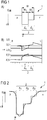
- FIG 1A a modification of an optoelectronic semiconductor chip 1 is schematically illustrated by the course of an indium content c and a bandgap E g along a growth direction z.
- An active quantum well 2 has a higher indium content c in comparison to the quantum well 2 surrounding regions of the semiconductor chip 1.
- the quantum well 2 comprises two zones A 1 , 2 .
- the indium content c is increased in comparison to the second zone A 2 .
- radiation generation preferably takes place approximately exclusively in the first zone A 1 .
- the semiconductor chip 1 is based, for example, on the InGaN material system.
- the band gap E g is given here in eV. As the indium content increases, the band gap E g decreases. For a band gap E g corresponding to a wavelength of about 450 nm, the indium content is preferably between 17% and 22% inclusive, corresponding to a wavelength of about 490 nm, preferably between 24% and 29% inclusive.
- the indium content c in the zones A 1 , A 2 is approximately constant in each case.
- the indium content c 1 of the first zone A 1 is 22% and the indium content c 2 of the second zone A 2 is approximately 12%.
- a width w 1 of the first zone A 1 is approximately 2.5 nm
- a width w 2 of the second zone A 2 is approximately 2 nm.
- a total width W of the active quantum well 2 is approximately 4.5 nm.
- the zones A 1 , 2 are consecutively numbered against the growth direction z of the semiconductor chip 1. The numbering therefore runs in a direction from a p-terminal side p to an n-terminal side n of the semiconductor chip 1.
- the indium content c i of the i-th zone is to be specified dimensionless in percent and the widths w i dimensionless in nanometers.
- N is the number of zones A 1 , 2 .
- the result is a value of: 22 ⁇ 2.5 + 12 ⁇ 2 - 2.5 ⁇ 2 - 1.5 ⁇ 2.5 + 2 ⁇ 67th
- FIG. 1B is a schematic of a course of the energies E of the valence band and the conduction band of the semiconductor chip 1 according to Figure 1A illustrated along the growth direction z.
- the band gap E g corresponds to the difference between the energies E of the valence band and the conduction band, in each case along the growth direction z.
- Wave functions of the valence band and the conduction band are each symbolized as thick lines, the corresponding energy levels as thin horizontal lines.
- An overlap range of the wave functions of the ground states of the valence band and the conduction band is comparatively large. In this way, in particular a high recombination rate of charge carriers, that is to say electrons and holes, in the quantum well 2 is made possible. Also, the trapping rate of carriers in the active quantum well 2 may be increased.
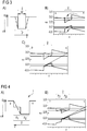
- FIG. 2 a further modification of a semiconductor chip 1 is schematically illustrated.
- the course of the indium content c along the growth direction z has three zones A 1 , 2 , 3 .
- Through the three zones of the active quantum well 2 is formed.
- As a dashed line an approximate mean indium content of the zones A 1 , 2 , 3 is shown.
- the real course of the indium content c has deviations therefrom, in particular in the areas of the edges of the dashed lines of the idealized course.
- the individual zones A 1 , 2 , 3 are clearly separated from one another by regions of a sharp increase or decrease in the indium content c.
- FIG. 3A a modification of a semiconductor device is shown in which the active quantum well 2 has a width W of about 6 nm and a mean indium content c of about 22%.
- FIGS. 3B and 3C only a relatively small overlap on each other.
- a gradient of the energies of the valence band and the conduction band in the area of the quantum well 2 due to piezoelectric fields is comparatively large, symbolized by an inclined dashed line in FIG FIG. 3C ,
- flanks of the quantum well 2 show a ramp-like course and a modified active quantum well 2 ', symbolized by a dash-and-dot line.
- FIG. 4 Another modification of the semiconductor chip 1 is shown in FIG. 4 shown.
- the zone A 2 with the highest indium content c 2 of the active quantum well 2 is adjacent in the direction of the p-terminal side p of a zone A 1 , which has a smaller mean indium content c 1 .
- the zone A 1 can also be ramp-shaped, indicated by a dash-dot line.
- FIG. 4B As in FIG. 4B can be seen is compared with FIG. 3C due to the zone A 1, the gradient of the energy E along the growth direction z in the region of the zone A 2 with the maximum indium content c 2 is significantly reduced, indicated in FIG. 4B through a thick line.
- the slope of the energy E of the quantum well 2 according to FIG. 3C drawn as a dash line.
- a gradient in the potential profile is reduced by the zone A 1 . This reduction of the gradient leads to an increased efficiency with respect to the radiation generation in the active quantum well 2.
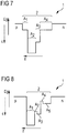
- the active quantum well 2 has three zones A 1 , 2 , 3 .
- the zone A 2 with the maximum indium content c 2 has the largest width w 2 .
- the indium content c 1 of the p-terminal-side zone A 1 is smaller than the indium content c 3 of the n-terminal-side zone A 3 .
- the quantum well 2 has a comparatively large effective width and thus a high Charge carrier capture rate. Also, the gradient is reduced in the potential curve. By local charges at the hetero boundaries between the zones A 1 , 3 and the surrounding semiconductor material outside the active quantum well 2 piezoelectric fields are reduced. As a result, a particularly high efficiency in the generation of radiation in the quantum well 2 can be achieved.
- the active quantum well 2 has three zones A 1 , 2 , 3 .
- the indium content c i rises monotone in the direction of growth z, starting from the zone A 1 .
- the step edge between the zones A 2 , 3 can, as indicated by a dotted line, for example, different, as in FIG. 6 drawn, rounded shape.
- the active quantum well 2 may also have significantly more than three zones A 1 , 2 , 3 .
- the active quantum well 2 has both a p-terminal-side zone A 1 and a plurality of n-terminal-side zones A 3 , 4 , which surround the zone A 2 with the maximum mean indium content c 2 .
- the active quantum well 2 has two intermediate barriers formed by the zones A 2 , 4 .
- the indium content c 2 , 4 of the zones A 2 , 4 is lowered in comparison to the respectively adjacent zones and / or an aluminum content of the zones is A 2 , 4 increased.
- FIG. 9 Furthermore, a p-terminal-side zone A 1 with a lower indium content c 1 is additionally present.
- the modification of the semiconductor chip 1 has two active quantum wells 2a, b.
- Each of the quantum wells 2a, b comprises two zones A 1 , 2 .
- the semiconductor chip 1 for example, have three, four, five or more active quantum wells.
- the semiconductor chip 1 also comprises an inactive quantum well 3.
- An indium content of the inactive quantum well 3 is, for example, between that of the zones A 1 , 2 of the active quantum wells 2a, b.
- the inactive quantum well 3 is located on the p-terminal side p of the semiconductor chip 1. Unlike in FIG. 11 it is also possible for the inactive quantum well 3 to comprise several zones with different indium content and / or aluminum content.
- FIG. 12 a modification is shown, according to which the inactive quantum well 3 can also be located on the n-terminal side n. It is also possible that groups with up to five inactive quantum wells 3 are formed on the n-connection side n and / or on the p-connection side p. In this case, it is not necessary that the different groups of inactive quantum wells 3 each have an equal number of inactive quantum wells 3. The same applies, see FIG. 13 , for an inactive quantum well 3 or a group with a plurality of inactive quantum wells 3 located between the active quantum wells 2a, b.
- the optoelectronic semiconductor chip 1 further includes two cladding layers 4a, b, which enclose or enclose the active quantum wells 2a, b.
- the semiconductor chip 1 furthermore has a respective barrier layer 6 between the active quantum well 2 and the waveguide layers 4a, b.
- the p-terminal-side waveguide layer 4a comprises a charge carrier barrier layer 5.
- the charge carrier barrier layer 5 is formed, for example, by a thin layer having an increased aluminum content.
- the semiconductor chip 1 can also have a plurality of active quantum wells 2 and optionally also one or more inactive quantum wells 3.
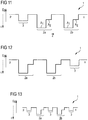
- FIGS. 16 and 17 a parameter variation with respect to the indium content c and the widths w of the zones A of the active quantum well 2 of semiconductor chips is schematically illustrated.
- the value of the term ⁇ c z dz - 2.5 N - 1.5 ⁇ dz is schematically illustrated.
- the active quantum well has two zones A each. Between FoM values of 40 and 80, in particular between 50 and 70, the semiconductor chips show a high efficiency, which manifests itself, for example, in a laser action. The same applies to the semiconductor chips according to FIG. 17 in which the active quantum well has three zones A in each case.
- an efficiency of the semiconductor chips in the given FoM value ranges is greater than outside these value ranges, the efficiency being the quotient of an emitted optical output power and an electrical input power with which the semiconductor chips are operated.
- the efficiency for FoM values outside the stated ranges may be less than 6%, and for FoM values in particular between 50 and 70, greater than or equal to 8 % be.
- the efficiency for FoM values outside the specified ranges is below 0.5%, and for FoM values in particular between 50 and 70 at least 0, 6%, preferably at least 0.8%.
- FIG. 18 1 illustrates a modification of a semiconductor chip 1 in which an aluminum content k is adjusted differently along the growth direction z of the active quantum well 2 into two zones A 1 , 2 .
- the aluminum content k and thicknesses of the zones A 1 , 2 are selected such that the active quantum well 2 satisfies the condition: 50 ⁇ ⁇ 35 - k z dz - 2.5 N - 1.5 ⁇ dz ⁇ 120th
- modification according to FIG. 18 may comprise inactive quantum wells, a plurality of active quantum wells and / or cladding layers and barrier layers, for example analogously to the modification according to FIG. 15 ,
Description
Es wird ein optoelektronischer Halbleiterchip angegeben.An optoelectronic semiconductor chip is specified.
Die Druckschrift
In der Druckschrift
Ein Licht emittierendes, GaN-III-V-Halbleiterbauteil findet sich in der Druckschrift
Es offenbart die Druckschrift
In der Druckschrift
Eine zu lösende Aufgabe besteht darin, einen optoelektronischen Halbleiterchip mit einer Quantentrogstruktur anzugeben, der im Betrieb Strahlung mit einer hohen Effizienz erzeugt.An object to be solved is to specify an optoelectronic semiconductor chip with a quantum well structure which generates radiation with high efficiency during operation.
Diese Aufgabe wird gelöst durch einen optoelektronischen Halbleiterchip mit den Merkmalen des Anspruchs 1.This object is achieved by an optoelectronic semiconductor chip having the features of
Gemäß der Erfindung basiert der optoelektronische Halbleiterchip auf einem Nitrid-Materialsystem. Mit anderen Worten ist eine Komponente des Halbleitermaterials, mit dem der Halbleiterchip hergestellt ist, Stickstoff. Bei dem Materialsystem handelt es sich also etwa um ein III-Nitrid-Halbleitermaterial. Zum Beispiel basiert der Halbleiterchip auf AlGaN, GaN, InGaN oder InAlGaN.According to the invention, the optoelectronic semiconductor chip is based on a nitride material system. With others In other words, a component of the semiconductor material with which the semiconductor chip is made is nitrogen. The material system is thus about a III-nitride semiconductor material. For example, the semiconductor chip is based on AlGaN, GaN, InGaN or InAlGaN.
Der optoelektronische Halbleiterchip ist epitaktisch gewachsen. Durch das epitaktische Wachsen ist eine Wachstumsrichtung z definiert.The optoelectronic semiconductor chip has grown epitaxially. The epitaxial growth defines a growth direction z.
Der optoelektronische Halbleiterchip umfasst mindestens einen aktiven Quantentrog. Der Begriff Quantentrog entfaltet hierbei keine Bedeutung hinsichtlich der Dimensionalität der Quantisierung. Der Quantentrog kann somit ein nulldimensionaler Quantenpunkt, ein eindimensionaler Quantendraht oder ein mehrdimensionaler Quantentopf oder jede Kombination dieser Strukturen darstellen.The optoelectronic semiconductor chip comprises at least one active quantum well. The term quantum trough has no significance with regard to the dimensionality of the quantization. The quantum well can thus represent a zero-dimensional quantum dot, a one-dimensional quantum wire or a multidimensional quantum well or any combination of these structures.
Gemäß zumindest einer Ausführungsform des optoelektronischen Halbleiterchips wird im Betrieb des Halbleiterchips in dem mindestens einen aktiven Quantentrog eine elektromagnetische Strahlung erzeugt. Eine Wellenlänge der elektromagnetischen Strahlung liegt bevorzugt im Spektralbereich zwischen 200 nm und 3000 nm, insbesondere im Spektralbereich zwischen einschließlich 360 nm und 540 nm.According to at least one embodiment of the optoelectronic semiconductor chip, an electromagnetic radiation is generated in the operation of the semiconductor chip in the at least one active quantum well. A wavelength of the electromagnetic radiation is preferably in the spectral range between 200 nm and 3000 nm, in particular in the spectral range between 360 nm and 540 nm inclusive.
Der mindestens eine aktive Quantentrog weist in einer Richtung parallel zu der Wachstumsrichtung z des Halbleiterchips N aufeinander folgende Zonen auf.The at least one active quantum well has, in a direction parallel to the growth direction z of the semiconductor chip N, successive zones.
Zumindest zwei der Zonen weisen einen voneinander verschiedenen mittleren Indiumgehalt c auf. Das heißt, innerhalb des aktiven Quantentrogs ist der Indiumgehalt gezielt variiert.At least two of the zones have a different mean indium content c from each other. This means, within the active quantum well, the indium content is deliberately varied.
Gemäß einer Abwandlung des Halbleiterchips erfüllt der aktive Quantentrog die folgende Bedingung: ![]()
![]()
Dass der mindestens eine aktive Quantentrog oben genannte Bedingung erfüllt, bedeutet, dass die Parameter Indiumgehalt c, Anzahl der Zonen N und Ausdehnung der Zonen sowie des aktiven Quantentrogs in einer Richtung parallel zur Wachstumsrichtung z so gewählt sind, dass das Integral über den Indiumgehalt c entlang der Wachstumsrichtung z innerhalb des aktiven Quantentrogs, subtrahiert um das 2,5-fache der Anzahl N der Zonen und subtrahiert um das 1,5-fache der Ausdehnung des aktiven Quantentrogs in einer Richtung parallel zur Wachstumsrichtung z zwischen einschließlich 40 und 80 liegt, bevorzugt zwischen einschließlich 50 und 70.The fact that the at least one active quantum well satisfies the above-mentioned condition means that the parameters indium content c, number of zones N and expansion of the zones and the active quantum well in a direction parallel to the growth direction z are chosen such that the integral extends along the indium content c the growth direction z within the active quantum well, subtracted by 2.5 times the number N of zones and subtracted by 1.5 times the extension of the active quantum well in a direction parallel to the growth direction z between 40 and 80 inclusive, is preferred between 50 and 70 inclusive.
Indiumgehalt bedeutet hierbei, dass ein Anteil der Nicht-Stickstoffgitterplätze durch Indiumatome substituiert ist.Indium content here means that a proportion of the non-nitrogen lattice sites is substituted by indium atoms.
Der Indiumgehalt c ist dimensionslos in Prozent anzugeben. Das heißt, c weist einen dimensionslosen Zahlenwert zwischen einschließlich 0 und 100 auf. Die Anzahl N der Zonen ist ebenfalls dimensionslos in obige Bedingung einzusetzen. z ist ebenso dimensionslos und entspricht einer Koordinate entlang einer Richtung parallel zur Wachstumsrichtung z in Nanometer.The indium content c is to be given dimensionless in percent. That is, c has a dimensionless number between 0 and 100 inclusive. The number N of zones must also be dimensionless in the above condition. z is also dimensionless and corresponds to a coordinate along a direction parallel to the growth direction z in nanometers.
Ein solcher aktiver Quantentrog weist bezüglich des Indiumgehalts entlang der Wachstumsrichtung zumindest abschnittsweise eine gestufte und/oder rampenartige Form auf.Such an active quantum well has at least in sections a stepped and / or ramp-like shape with respect to the indium content along the growth direction.
Durch diese rampenartige und/oder gestufte Struktur des aktiven Quantentrogs kann sich ein Überlapp der Wellenfunktionen im Valenzband und im Leitungsband erhöhen. Der vergrößerte Überlapp der Wellenfunktionen kann zu einer gesteigerten Effizienz des Halbleiterchips führen.As a result of this ramp-like and / or stepped structure of the active quantum well, an overlap of the wave functions in the valence band and in the conduction band can increase. The increased overlap of the wave functions can lead to increased efficiency of the semiconductor chip.
Ferner kann eine Ladungsträgereinfangrate erhöht sein. Mit anderen Worten wird mit hoher Wahrscheinlichkeit ein Ladungsträger, beispielsweise ein Elektron, in dem aktiven Quantentrog eingefangen und kann zur Strahlung emittierenden Rekombination dienen. Durch die Ausbildung von Heterogrenzen durch eine oder mehrere Stufen im Bereich einer Bandkante können lokalisierte Grenzflächenladungen erzeugt werden. Durch diese lokalisierten Grenzflächenladungen können zusätzlich Piezofelder reduziert sein, wodurch ebenfalls eine Effizienz der Strahlungserzeugung des Halbleiterchips gesteigert sein kann.Further, a charge trapping rate may be increased. In other words, a charge carrier, for example an electron, is trapped in the active quantum well with high probability and can serve for radiation-emitting recombination. By forming hetero boundaries through one or more steps in the region of a band edge, localized interfacial charges can be generated. In addition, piezoelectric fields can be reduced by these localized interface charges, as a result of which an efficiency of the radiation generation of the semiconductor chip can likewise be increased.
Die obige Bedingung bezüglich der Parameter des Quantentrogs, insbesondere im Hinblick auf die Dicken der Zonen und auf deren Indiumgehalt, gibt einen Parameterbereich zur Gestaltung des aktiven Quantentrogs an, über den eine überraschend hohe Effizienz und somit ein besonders hoher Wirkungsgrad bei der Strahlungserzeugung des Halbleiterchips erzielbar ist.The above condition regarding the parameters of the quantum well, in particular with regard to the thicknesses of the zones and their indium content, indicates a parameter range for designing the active quantum well, via which a surprisingly high efficiency and thus a particularly high efficiency in the radiation generation of the semiconductor chip can be achieved is.
Der Wertebereich, den der Term ∫c(z)dz-2,5N-1,5∫dz annehmen kann, unterliegt hierbei keinen prinzipiellen Beschränkungen. Beispielsweise kann der Term für herkömmliche aktive Quantentröge 200 übersteigen oder auch kleiner als 0 sein.The range of values that can be assumed by the term ∫ c ( z ) dz -2.5 N- 1.5∫ dz is not subject to any fundamental restrictions. For example, the term for conventional active quantum wells 200 may exceed 200, or may be less than zero.
Gemäß der Erfindung erfüllt der mindestens eine aktive Quantentrog des optoelektronischen Halbleiterchips die folgende Bedingung: 

ci ist hierbei der mittlere Indiumgehalt der i-ten Zone und wi eine Breite der i-ten Zone des mindestens einen aktiven Quantentrogs. Die Zonen des Quantentrogs sind in Richtung parallel zur Wachstumsrichtung z des Halbleiterchips fortlaufend nummeriert.Here, c i is the mean indium content of the ith zone and w i is a width of the ith zone of the at least one active quantum well. The zones of the quantum tray are numbered consecutively in the direction parallel to the growth direction z of the semiconductor chip.
Beispielsweise ist eine Zone des aktiven Quantentopfs ein solcher Bereich, in dem der Indiumgehalt entlang der Wachstumsrichtung z lokal von einem über die gesamte Zone gemittelten Indiumgehalt um höchstens 30 %, bevorzugt um höchstens 15 %, abweicht. Mit anderen Worten bilden zum Beispiel ausgeprägte, stufenartige Anstiege oder Abfälle des Indiumgehalts Grenzen oder Grenzgebiete zwischen benachbarten Zonen.For example, a zone of the active quantum well is such a region in which the indium content along the growth direction z deviates locally from an indium content averaged over the entire zone by at most 30%, preferably by at most 15%. In other words, for example, pronounced, step-like rises or drops in indium content form boundaries or border areas between adjacent zones.
Der Indiumgehalt c ist innerhalb der Zonen des mindestens einen aktiven Quantentrogs jeweils konstant, unter Berücksichtigung der Herstellungstoleranzen. Zum Beispiel kann konstant bedeuten, dass der Indiumgehalt c innerhalb der Zonen Abweichungen von einem Mittelwert um höchstens 2 Prozentpunkte, insbesondere um höchstens 1 Prozentpunkt, aufzeigt. Der Begriff konstant schließt beispielsweise nicht aus, dass Stufenkanten im Verlauf des Indiumgehalts längs einer Richtung parallel zur Wachstumsrichtung eine abgerundete Form aufweisen können. Mit anderen Worten ist der Verlauf des Indiumgehalts durch eine Stufenfunktion approximierbar.The indium content c is in each case constant within the zones of the at least one active quantum well, taking into account the manufacturing tolerances. For example, it may be constant that the indium content c within the zones deviates from a mean by at most 2 percentage points, in particular by at most 1 percentage point, shows. For example, the term constant does not exclude that step edges in the course of indium content along a direction parallel to the growth direction may have a rounded shape. In other words, the course of the indium content can be approximated by a step function.
Der mindestens eine aktive Quantentrog weist mindestens drei Zonen auf. Mit anderen Worten ist N größer oder gleich 3. Es weisen mindestens drei Zonen, bevorzugt alle Zonen, jeweils einen unterschiedlichen mittleren Indiumgehalt auf.The at least one active quantum well has at least three zones. In other words, N is greater than or equal to 3. At least three zones, preferably all zones, each have a different mean indium content.
Gemäß der Erfindung weist der optoelektronische Halbleiterchip eine p-Anschlussseite und eine n-Anschlussseite auf. An der p-Anschlussseite des Halbleiterchips befindet sich zum Beispiel p-dotiertes Halbleitermaterial und an der n-Anschlussseite n-dotiertes Halbleitermaterial. Über die Anschlussseiten ist der Halbleiterchip bevorzugt elektrisch kontaktierbar.According to the invention, the optoelectronic semiconductor chip has a p-connection side and an n-connection side. For example, p-doped semiconductor material is located on the p-terminal side of the semiconductor chip and n-doped semiconductor material is on the n-terminal side. The semiconductor chip can preferably be electrically contacted via the connection sides.
Gemäß der Erfindung gilt für den mittleren Indiumgehalt c zumindest eines Teils der Zonen:
ci < ci+1 und ci+1 > ci+2.According to the invention, for the mean indium content c of at least a part of the zones:
c i <c i + 1 and c i + 1 > c i + 2 .
Die Zonen sind parallel zur Wachstumsrichtung von der p-Anschlussseite hin zur n-Anschlussseite fortlaufend nummeriert. Bevorzugt ist i = 1. Mit anderen Worten weist der aktive Quantentrog eine zentrale Zone mit einem hohen Indiumgehalt auf, die beidseitig von Zonen mit einem herabgesetzten Indiumgehalt umgeben ist.The zones are numbered consecutively parallel to the growth direction from the p-connection side to the n-connection side. I = 1 is preferred. In other words, the active quantum well has a central zone with a high indium content, which is surrounded on both sides by zones with a reduced indium content.
Gemäß der Erfindung gilt weiterhin, dass ci < ci+2. Mit anderen Worten weist der aktive Quantentrog eine zentrale Zone mit einem hohen Indiumgehalt auf. Eine Zone, die sich näher an der p-Anschlussseite als die zentrale Zone befindet, weist einen kleineren Indiumgehalt auf als die Zone, die sich näher an der n-Anschlussseite befindet.
Gemäß zumindest einer Ausführungsform des optoelektronischen Halbleiterchips gilt, in einer Richtung von der p-Anschlussseite hin zur n-Anschlussseite, für den mittleren Indiumgehalt für einen Teil der Zonen:
ci > ci+1 und ci+2 > ci+1 und ci > ci+2.
Mit anderen Worten ist die Zone i+1 von zwei Zonen mit einem höheren Indiumgehalt umgeben. Die Zone i+1 stellt zum Beispiel eine Zwischenbarriere in dem Quantentrogprofil dar. Bevorzugt ist i = 1 oder i = 2.
Gemäß zumindest einer Ausführungsform des optoelektronischen Halbleiterchips umfasst der mindestens eine aktive Quantentrog zwischen einschließlich drei und zehn Zonen. Mit anderen Worten gilt: 3 ≤ N ≤ 10, bevorzugt 3 ≤ N ≤ 6.
Gemäß zumindest einer Ausführungsform des optoelektronischen Halbleiterchips beträgt eine Gesamtbreite des aktiven Quantentrogs zwischen einschließlich 0,25 nm und 12 nm, insbesondere zwischen einschließlich 0,5 nm und 10 nm, bevorzugt zwischen einschließlich 3,5 nm und 8 nm.
Gemäß zumindest einer Ausführungsform des optoelektronischen Halbleiterchips befindet sich eine Zone mit geringerer Breite zwischen zwei Zonen größerer Breite.According to the invention, furthermore, c i <c i + 2 . In other words, the active quantum well has a central zone with a high indium content. A zone closer to the p-terminal side than the central zone has a smaller indium content than the zone closer to the n-terminal side.
According to at least one embodiment of the optoelectronic semiconductor chip, in a direction from the p-terminal side to the n-terminal side, for the mean indium content for a part of the zones:
c i > c i + 1 and c i + 2 > c i + 1 and c i > c i + 2 .
In other words, zone i + 1 is surrounded by two zones of higher indium content. For example, zone i + 1 represents an intermediate barrier in the quantum well profile. Preferably i = 1 or i = 2.
In accordance with at least one embodiment of the optoelectronic semiconductor chip, the at least one active quantum well comprises between three and ten zones inclusive. In other words, 3 ≦ N ≦ 10, preferably 3 ≦ N ≦ 6.
According to at least one embodiment of the optoelectronic semiconductor chip, a total width of the active quantum well is between 0.25 nm and 12 nm inclusive, in particular between 0.5 nm and 10 nm inclusive, preferably between 3.5 nm and 8 nm inclusive.
In accordance with at least one embodiment of the optoelectronic semiconductor chip There is a zone of lesser width between two zones of greater width.
Gemäß zumindest einer Ausführungsform des optoelektronischen Halbleiterchips gilt bezüglich der Breiten w für zumindest einen Teil der Zonen des aktiven Quantentrogs:
wi < wi+1 und wi < wi+2.
Bevorzugt ist hierbei die Zone i+1 diejenige Zone mit dem höchsten Indiumgehalt. Es ist also bevorzugt i = 1. Weiterhin kann insbesondere wi+1 > wi+2 gelten.
Gemäß zumindest einer Ausführungsform des optoelektronischen Halbleiterchips ist eine Breite in einer Richtung parallel zur Wachstumsrichtung z der mindestens einen Zwischenbarriere des aktiven Quantentrogs kleiner als eine minimale Breite der weiteren Zonen des mindestens einen aktiven Quantentrogs. Mit anderen Worten ist die Zwischenbarriere dünn gestaltet. Insbesondere weist die Zwischenbarriere eine Dicke entlang der Wachstumsrichtung zwischen einschließlich 0,25 nm und 1,25 nm auf.
Gemäß zumindest einer Ausführungsform des optoelektronischen Halbleiterchips liegen die Dicken der Zonen, mit Ausnahme der Dicken von gegebenenfalls vorhandenen Zwischenbarrieren, zwischen einschließlich 1,5 nm und 4 nm, insbesondere zwischen einschließlich 1,75 nm und 3 nm.In accordance with at least one embodiment of the optoelectronic semiconductor chip, with regard to the widths w for at least part of the zones of the active quantum well, the following applies:
w i <w i + 1 and w i <w i + 2 .
In this case, the zone i + 1 is preferably the zone with the highest indium content. It is therefore preferred i = 1. Furthermore, in particular w i + 1 > w i + 2 apply.
In accordance with at least one embodiment of the optoelectronic semiconductor chip, a width in a direction parallel to the growth direction z of the at least one intermediate barrier of the active quantum well is smaller than a minimum width of the further zones of the at least one active quantum well. In other words, the intermediate barrier is made thin. In particular, the intermediate barrier has a thickness along the growth direction between 0.25 nm and 1.25 nm inclusive.
According to at least one embodiment of the optoelectronic semiconductor chip, the thicknesses of the zones are, with the exception of the thicknesses of any intermediate barriers present, between 1.5 nm and 4 nm, in particular between 1.75 nm and 3 nm.
Gemäß zumindest einer Ausführungsform des optoelektronischen Halbleiterchips liegt ein Indiumgehalt der Zone mit dem höchsten Indiumgehalt zwischen einschließlich 15 % und 50 %.According to at least one embodiment of the optoelectronic semiconductor chip, an indium content of the zone with the highest indium content is between 15% and 50% inclusive.
Gemäß zumindest einer Ausführungsform des optoelektronischen Halbleiterchips beträgt ein Indiumgehalt zumindest einer Zone, die der Zone mit dem maximalen Indiumgehalt benachbart ist, zwischen einschließlich 30 % und 80 %, insbesondere zwischen einschließlich 40 % und 60 % des mittleren Indiumgehalts der Zone mit dem maximalen Indiumgehalt.According to at least one embodiment of the optoelectronic semiconductor chip, an indium content of at least one zone adjacent to the zone of maximum indium content is between 30% and 80%, in particular between 40% and 60% of the mean indium content of the zone with the maximum indium content.
Gemäß zumindest einer Ausführungsform des optoelektronischen Halbleiterchips gilt für den mittleren Indiumgehalt mindestens einer i-ten Zone, wobei bevorzugt i = 2 oder i > 2 ist: ![]()
![]()
![]()
![]()
Gemäß zumindest einer Ausführungsform des optoelektronischen Halbleiterchips umfasst dieser, in einer Richtung parallel zur Wachstumsrichtung z, zwischen einschließlich zwei und fünf aktive Quantentröge. Mit anderen Worten weist der Halbleiterchip eine Multiquantentrogstruktur auf.According to at least one embodiment of the optoelectronic semiconductor chip, this comprises, in a direction parallel to the growth direction z, between two and five active quantum wells inclusive. In other words, the semiconductor chip has a multi-quantum well structure.
Gemäß zumindest einer Ausführungsform des optoelektronischen Halbleiterchips umfasst dieser mindestens einen inaktiven Quantentrog. Ein mittlerer Indiumgehalt des inaktiven Quantentrogs ist hierbei kleiner als der mittlerer Indiumgehalt der Zonen des mindestens einen aktiven Quantentrogs, die dem maximalen mittleren Indiumgehalt aufweist.According to at least one embodiment of the optoelectronic semiconductor chip, the latter comprises at least one inactive one Quantum well. A mean indium content of the inactive quantum well is smaller than the mean indium content of the zones of the at least one active quantum well, which has the maximum mean indium content.
Inaktiv bedeutet, dass der inaktive Quantentrog nicht zu einer Strahlungserzeugung eingerichtet ist. Im Betrieb des Halbleiterchips wird also in dem mindestens einen inaktiven Quantentrog kein oder nur ein vernachlässigbar kleiner Anteil an der emittierten Strahlung erzeugt. Bevorzugt beträgt der in den inaktiven Quantentrögen erzeugte Strahlungsanteil weniger als 10 %, insbesondere weniger als 2 %.Inactive means that the inactive quantum well is not set up for generating radiation. During operation of the semiconductor chip, therefore, no or only a negligibly small proportion of the emitted radiation is generated in the at least one inactive quantum well. Preferably, the proportion of radiation generated in the inactive quantum wells is less than 10%, in particular less than 2%.
Gemäß zumindest einer Ausführungsform des optoelektronischen Halbleiterchips ist eine Dicke des inaktiven Quantentrogs kleiner als eine Dicke des aktiven Quantentrogs, entlang einer Richtung parallel zur Wachstumsrichtung z. Bevorzugt beträgt die Dicke des inaktiven Quantentrogs höchstens 75 % der Dicke des aktiven Quantentrogs.According to at least one embodiment of the optoelectronic semiconductor chip, a thickness of the inactive quantum well is smaller than a thickness of the active quantum well, along a direction parallel to the growth direction z. Preferably, the thickness of the inactive quantum well is at most 75% of the thickness of the active quantum well.
Gemäß zumindest einer Ausführungsform des optoelektronischen Halbleiterchips umfasst dieser mindestens zwei inaktive Quantentröge, die den mindestens einen aktiven Quantentrog einschließen.In accordance with at least one embodiment of the optoelectronic semiconductor chip, the latter comprises at least two inactive quantum wells, which enclose the at least one active quantum well.
Gemäß zumindest einer Ausführungsform des optoelektronischen Halbleiterchips befindet sich zwischen zwei benachbarten aktiven Quantentrögen wenigstens ein inaktiver Quantentrog, insbesondere zwischen einschließlich einem und fünf inaktiven Quantentrögen. Bevorzugt befindet sich auch zwischen der p-Anschlussseite und dem der p-Anschlussseite nächstgelegenen aktiven Quantentrog mindestens ein inaktiver Quantentrog, insbesondere zwischen einschließlich einem und fünf inaktiven Quantentrögen. Entsprechendes gilt bevorzugt auch für den der n-Anschlussseite nächstgelegenen aktiven Quantentrog.According to at least one embodiment of the optoelectronic semiconductor chip, at least one inactive quantum well is located between two adjacent active quantum wells, in particular between one and five inactive quantum wells. Preferably, at least one inactive quantum well is also located between the p connection side and the active quantum well closest to the p connection side, especially between one and five inactive quantum wells. The same applies preferably also for the active quantum well closest to the n-connection side.
Gemäß zumindest einer Ausführungsform des optoelektronischen Halbleiterchips weist dieser wenigstens zwei Wellenleiterschichten auf, wobei sich der mindestens eine aktive Quantentrog, insbesondere alle aktiven Quantentröge, zwischen den Wellenleiterschichten befinden. Mit anderen Worten ist der mindestens eine aktive Quantentrog von den Wellenleiterschichten eingeschlossen.According to at least one embodiment of the optoelectronic semiconductor chip, the latter has at least two waveguide layers, wherein the at least one active quantum well, in particular all active quantum wells, are located between the waveguide layers. In other words, the at least one active quantum well is enclosed by the waveguide layers.
Gemäß zumindest einer Ausführungsform des optoelektronischen Halbleiterchips beinhaltet zumindest eine der Wellenleiterschichten eine oder mehrere Ladungsträgerbarriereschichten. Bei der Ladungsträgerbarriereschicht handelt es sich beispielsweise um eine Elektronenbarriereschicht, die in der p-anschlussseitigen Wellenleiterschicht eingebracht ist. Die Ladungsträgerbarriereschicht kann einen erhöhten Al-Gehalt und eine geringe Dicke zwischen einschließlich 0,25 nm und 20 nm aufweisen.In accordance with at least one embodiment of the optoelectronic semiconductor chip, at least one of the waveguide layers contains one or more charge carrier barrier layers. The carrier barrier layer is, for example, an electron barrier layer incorporated in the p-terminal side waveguide layer. The charge carrier barrier layer may have an increased Al content and a small thickness between 0.25 nm and 20 nm inclusive.
Gemäß zumindest einer Ausführungsform des optoelektronischen Halbleiterchips ist dieser zur Erzeugung einer Laserstrahlung eingerichtet. Mit anderen Worten ist der Halbleiterchip ein Laserchip.In accordance with at least one embodiment of the optoelectronic semiconductor chip, the latter is set up to generate a laser radiation. In other words, the semiconductor chip is a laser chip.
Gemäß zumindest einer Ausführungsform des optoelektronischen Halbleiterchips ist dieser zur Erzeugung einer elektromagnetischen Strahlung zwischen einschließlich 430 nm und 540 nm eingerichtet. Mit anderen Worten emittiert der Halbleiterchip im blauen und/oder grünen Spektralbereich.In accordance with at least one embodiment of the optoelectronic semiconductor chip, this is set up to generate electromagnetic radiation of between 430 nm and 540 nm inclusive. In other words, the semiconductor chip emits in the blue and / or green spectral range.
Darüber hinaus wird in einer nicht erfindungsgemäßen Abwandlung ein optoelektronischer Halbleiterchip angegeben, bei dem ein Aluminiumgehalt in mindestens einem aktiven Quantentrog variiert ist.In addition, in an embodiment not according to the invention, an optoelectronic semiconductor chip is specified in which an aluminum content in at least one active quantum well is varied.
In einer nicht erfindungsgemäßen Abwandlung des optoelektronischen Halbleiterchips basiert dieser auf einem Nitrid-Materialsystem und weist mindestens einen aktiven Quantentrog auf, wobei in dem aktiven Quantentrog im Betrieb eine elektromagnetische Strahlung erzeugt wird. In einer Richtung parallel zu einer Wachstumsrichtung z des Halbleiterchips weist dieser N aufeinander folgende Zonen auf, wobei zumindest zwei der Zonen einen voneinander verschiedenen mittleren Aluminiumgehalt k aufweisen und N eine natürliche Zahl größer oder gleich 2 ist. Der mindestens eine aktive Quantentrog erfüllt hierbei die Bedingung: ![]()
![]()
![]()
![]()
Merkmale des Halbleiterchips, bei dem der mittlere Indiumgehalt der Zonen des aktiven Quantentrogs variiert ist, sind auch für die hier beschriebene nicht erfindungsgemäße Abwandlung des Halbleiterchips mit variiertem Aluminiumgehalt offenbart. Da mit zunehmendem Indiumgehalt eine Bandlücke abnimmt und mit zunehmendem Aluminiumgehalt eine Bandlücke zunimmt, sind Relationszeichen bezüglich des Indiumgehalts für den Fall eines variierten mittleren Aluminiumgehalts der Zonen des aktiven Quantentrogs entsprechend umzukehren.Features of the semiconductor chip in which the mean indium content of the zones of the active quantum well is varied are also for the non-inventive modification of the semiconductor chip with varied aluminum content described here disclosed. Since a bandgap decreases with increasing indium content and a bandgap increases with increasing aluminum content, relative terms for the indium content in the case of a varied average aluminum content of the zones of the active quantum well are to be correspondingly reversed.
Einige Anwendungsbereiche, in denen hier beschriebene optoelektronische Halbleiterchips Verwendung finden können, sind etwa die Hinterleuchtungen von Displays oder Anzeigeeinrichtungen. Weiterhin können hier beschriebene Halbleiterchips auch in Beleuchtungseinrichtungen zu Projektionszwecken, in Scheinwerfern oder Lichtstrahlern oder bei der Allgemeinbeleuchtung eingesetzt werden.Some application areas in which optoelectronic semiconductor chips described here can be used are, for example, the backlighting of displays or display devices. Furthermore, semiconductor chips described here can also be used in illumination devices for projection purposes, in headlights or light emitters or in general lighting.
Nachfolgend wird ein hier beschriebener optoelektronischer Halbleiterchip unter Bezugnahme auf die Zeichnung anhand von Ausführungsbeispielen und nicht erfindungsgemäßen Abwandlungen näher erläutert. Gleiche Bezugszeichen geben dabei gleiche Elemente in den einzelnen Figuren an. Es sind dabei jedoch keine maßstäblichen Bezüge dargestellt, vielmehr können einzelne Elemente zum besseren Verständnis übertrieben groß dargestellt sein.Hereinafter, an optoelectronic semiconductor chip described here will be explained in more detail with reference to the drawings based on embodiments and modifications not according to the invention. The same reference numerals indicate the same elements in the individual figures. However, there are no scale relationships shown, but individual elements can be shown exaggerated for better understanding.
Es zeigen:
Figuren 1- eine schematische Schnittdarstellung einer Abwandlung eines Halbleiterchips (A) und eine schematische Darstellung dessen Bandstruktur (B),
Figur 2- eine schematische Darstellung einer weiteren Abwandlung eines optoelektronischen Halbleiterchips,
Figur 3- eine schematische Darstellung einer Abwandlung eines Halbleiterbauteils,
Figuren 4, 6, 8 und bis 15- schematische Darstellungen von weiteren Abwandlungen von optoelektronischen Halbleiterchips,
- Figuren 5, 7 und 9
- schematische Darstellungen von Ausführungsbeispielen von hier beschriebenen optoelektronischen Halbleiterchips,
- Figuren 16 und 17
- schematische Darstellungen von Parametervariationen von Halbleiterchips, und
- Figur 18
- eine schematische Darstellung einer Abwandlung eines optoelektronischen Halbleiterchips mit Zonen mit unterschiedlichem Aluminiumgehalt.
- FIGS. 1
- 1 is a schematic sectional view of a modification of a semiconductor chip (A) and a schematic illustration of its band structure (B),
- FIG. 2
- a schematic representation of a further modification of an optoelectronic semiconductor chip,
- FIG. 3
- a schematic representation of a modification of a semiconductor device,
- FIGS. 4, 6, 8 and 15
- schematic representations of further modifications of optoelectronic semiconductor chips,
- FIGS. 5, 7 and 9
- schematic representations of embodiments of optoelectronic semiconductor chips described herein,
- FIGS. 16 and 17
- schematic representations of parameter variations of semiconductor chips, and
- FIG. 18
- a schematic representation of a modification of an optoelectronic semiconductor chip with zones with different aluminum content.
In
Der Halbleiterchip 1 beruht beispielsweise auf dem InGaN-Materialsystem. Die Bandlücke Eg kann, für einen Indiumgehalt x in Prozent, näherungsweise wie folgt angegeben werden, siehe auch die ![]()
![]()
Die Bandlücke Eg ist hierbei in eV angegeben. Mit zunehmendem Indiumgehalt nimmt die Bandlücke Eg ab. Für eine Bandlücke Eg, entsprechend einer Wellenlänge von zirka 450 nm, beträgt der Indiumgehalt bevorzugt zwischen einschließlich 17 % und 22 %, entsprechend einer Wellenlänge von zirka 490 nm bevorzugt zwischen einschließlich 24 % und 29 %.The band gap E g is given here in eV. As the indium content increases, the band gap E g decreases. For a band gap E g corresponding to a wavelength of about 450 nm, the indium content is preferably between 17% and 22% inclusive, corresponding to a wavelength of about 490 nm, preferably between 24% and 29% inclusive.
Näherungsweise ist der Indiumgehalt c in den Zonen A1, A2 jeweils konstant. Beispielsweise beträgt der Indiumgehalt c1 der ersten Zone A1 22 % und der Indiumgehalt c2 der zweiten Zone A2 zirka 12 %. Eine Breite w1 der ersten Zone A1 liegt bei zirka 2,5 nm, eine Breite w2 der zweiten Zone A2 bei zirka 2 nm. Somit beträgt eine Gesamtbreite W des aktiven Quantentrogs 2 zirka 4,5 nm. Die Zonen A1, 2 sind entgegen der Wachstumsrichtung z des Halbleiterchips 1 fortlaufend nummeriert. Die Nummerierung verläuft also in einer Richtung von einer p-Anschlussseite p hin zu einer n-Anschlussseite n des Halbleiterchips 1.The indium content c in the zones A 1 , A 2 is approximately constant in each case. For example, the indium content c 1 of the first zone A 1 is 22% and the indium content c 2 of the second zone A 2 is approximately 12%. A width w 1 of the first zone A 1 is approximately 2.5 nm, a width w 2 of the second zone A 2 is approximately 2 nm. Thus, a total width W of the active
Wegen des in den Zonen A1, 2 konstanten Indiumgehalts c kann der Term ∫c(z)dz-2,5N-1,5∫dz durch den Term 
![]()
![]()
Es ist möglich, den Wert des Terms für den aktiven Quantentrog 2 über ein Ausmessen des Quantentrogs 2 etwa mittels Elektronenmikroskopie, insbesondere Transmissionselektronenmikroskopie, zu ermitteln.It is possible to determine the value of the term for the active quantum well 2 by measuring the
In
In
In den nachfolgend beschriebenen Ausführungsbeispielen und nicht erfindungsgemäßen Abwandlungen ist jeweils ein durch Stufen angenäherter, idealisierter Indiumgehalt c längs der Wachstumsrichtung z illustriert. Es ist also möglich, dass Abweichungen des Indiumgehalts c von den gezeigten Verläufen auftreten, analog zu
In 
Es ist möglich, dass die Flanken des Quantentrogs 2 einen rampenartigen Verlauf aufzeigen und sich ein modifizierter aktiver Quantentrog 2' ergibt, symbolisiert durch eine Strich-Punkt-Linie.It is possible that the flanks of the quantum well 2 show a ramp-like course and a modified active quantum well 2 ', symbolized by a dash-and-dot line.
Eine weitere Abwandlung des Halbleiterchips 1 ist in
Wie in
Beim Ausführungsbeispiel des Halbleiterchips 1 gemäß
Wie in
Bei der Abwandlung gemäß
Beim Ausführungsbeispiel gemäß
Bei der Abwandlung des Halbleiterchips 1 gemäß
Gemäß
Gemäß der Abwandlung nach
In
Gemäß der Abwandlung nach
Bei der Abwandlung gemäß
Anders als in
Bei den Abwandlungen beziehungsweise Beispielen des Halbleiterchips 1 gemäß der ![]()

![]()
In den ![]()
![]()
kurz FoM, entlang der Abszissenachse aufgetragen. Gemäß
Beispielsweise ist ein Wirkungsgrad der Halbleiterchips in den angegebenen FoM-Wertebereichen größer als außerhalb dieser Wertebereiche, wobei der Wirkungsgrad der Quotient aus einer emittierten optischen Ausgangsleistung und einer elektrischen Eingangsleistung, mit der die Halbleiterchips betrieben werden, ist. Bei einer Wellenlänge der emittierten Strahlung von zirka 440 nm und einer optischen Ausgangsleistung von 30 mW kann der Wirkungsgrad für FoM-Werte außerhalb der angegebenen Bereiche kleiner als 6 % sein, und für FoM-Werte insbesondere zwischen einschließlich 50 und 70 größer als oder gleich 8 % sein. Für eine Wellenlänge von zirka 480 nm und einer Ausgangsleistung von 5 mW ist es möglich, dass der Wirkungsgrad für FoM-Werte außerhalb der angegebenen Bereiche unterhalb von 0,5 % liegt, und für FoM-Werte insbesondere zwischen einschließlich 50 und 70 mindestens 0,6 %, bevorzugt mindestens 0,8 % beträgt.By way of example, an efficiency of the semiconductor chips in the given FoM value ranges is greater than outside these value ranges, the efficiency being the quotient of an emitted optical output power and an electrical input power with which the semiconductor chips are operated. At a wavelength of the emitted radiation of approximately 440 nm and an optical output power of 30 mW, the efficiency for FoM values outside the stated ranges may be less than 6%, and for FoM values in particular between 50 and 70, greater than or equal to 8 % be. For a wavelength of approximately 480 nm and an output power of 5 mW it is possible that the efficiency for FoM values outside the specified ranges is below 0.5%, and for FoM values in particular between 50 and 70 at least 0, 6%, preferably at least 0.8%.
In ![]()
![]()
Auch die Abwandlung gemäß
Auch ist es möglich, dass eine Einstellung des Aluminiumgehalts k der Zonen A des aktiven Quantentrogs 2 mit einer Einstellung des Indiumgehalts c, etwa gemäß den
Claims (9)
- An optoelectronic semiconductor chip (1), based on a nitride material system, comprising at least one active quantum well (2), wherein- an electromagnetic radiation is generated in the active quantum well (2) during operation,- in a direction parallel to a growth direction z of the semiconductor chip (1), the active quantum well (2) comprises N consecutive zones (A) and N is a natural number greater than or equal to 3,- at least two of the zones (A) have a different mean indium content c, and- the active quantum well (2) satisfies the condition:

wherein the indium content c within the zones (A) of the at least one active quantum well (2) is in each case constant, wherein the indium content c being specified dimensionless in percent and w being specified dimensionless in nanometers, wherein, in a direction parallel to the growth direction z and from a p-connection side (p) to an n-connection side (n) of the semiconductor chip (1), for the average indium content for at least some of the zones (A) it applies:
ci < ci+1 and ci+1 > ci+2,
characterized in that
ci < ci+2. - The optoelectronic semiconductor chip (1) according to the preceding claim,
in which, in a direction parallel to the growth direction z and from the p-connection side (P) to the n-connection side (n) of the semiconductor chip (1), for the average indium content for a part of the zones (A) it applies:cj > cj+1 and cj+2 > cj+1 and cj > cj+2,wherein the zones (A) are continuously numbered with j in a direction parallel to the growth direction z. - The optoelectronic semiconductor chip (1) according to one of the preceding claims,
wherein N is between 3 and 10 inclusive and in which a total width (W) of the active quantum well (2) is between 0.25 nm and 12 nm inclusive. - The optoelectronic semiconductor chip (1) according to one of the preceding claims,
comprising between 2 and 5 inclusive active quantum wells (2), in a direction parallel to the growth direction z. - The optoelectronic semiconductor chip (1) according to one of the preceding claims,
comprising at least two inactive quantum wells (3),
wherein an indium content of the inactive quantum wells (3) is smaller than a maximum indium content of the at least one active quantum well (2). - The optoelectronic semiconductor chip (1) according to claims 4 and 5,
in which at least one inactive quantum well (3) is located between at least two adjacent active quantum wells (2). - The an optoelectronic semiconductor chip (1) according to one of the preceding claims,
comprising at least two waveguide layers (4),
wherein the at least one active quantum well (2) is located between the waveguide layers (4), and
wherein at least one of the waveguide layers (4) contains at least one charge carrier barrier layer (5). - The optoelectronic semiconductor chip (1) according to one of the preceding claims,
which is configured to generate a laser radiation. - The optoelectronic semiconductor chip (1) according to one of the preceding claims,
which is configured to generate an electromagnetic radiation between 430 nm and 540 nm inclusive.
Applications Claiming Priority (2)
| Application Number | Priority Date | Filing Date | Title |
|---|---|---|---|
| DE102009015569.4A DE102009015569B9 (en) | 2009-03-30 | 2009-03-30 | Optoelectronic semiconductor chip |
| PCT/EP2010/053047 WO2010112310A1 (en) | 2009-03-30 | 2010-03-10 | Optoelectronic semiconductor chip |
Publications (2)
| Publication Number | Publication Date |
|---|---|
| EP2415085A1 EP2415085A1 (en) | 2012-02-08 |
| EP2415085B1 true EP2415085B1 (en) | 2019-01-02 |
Family
ID=42340450
Family Applications (1)
| Application Number | Title | Priority Date | Filing Date |
|---|---|---|---|
| EP10707304.1A Active EP2415085B1 (en) | 2009-03-30 | 2010-03-10 | Optoelectronic semiconductor chip |
Country Status (8)
| Country | Link |
|---|---|
| US (2) | US8908733B2 (en) |
| EP (1) | EP2415085B1 (en) |
| JP (3) | JP2012522390A (en) |
| KR (2) | KR101645057B1 (en) |
| CN (2) | CN104319331B (en) |
| DE (1) | DE102009015569B9 (en) |
| TW (1) | TWI452723B (en) |
| WO (1) | WO2010112310A1 (en) |
Families Citing this family (16)
| Publication number | Priority date | Publication date | Assignee | Title |
|---|---|---|---|---|
| DE102009015569B9 (en) * | 2009-03-30 | 2023-06-29 | OSRAM Opto Semiconductors Gesellschaft mit beschränkter Haftung | Optoelectronic semiconductor chip |
| KR101712049B1 (en) | 2010-11-17 | 2017-03-03 | 엘지이노텍 주식회사 | Light emitting device |
| JP5417307B2 (en) * | 2010-12-02 | 2014-02-12 | 株式会社東芝 | Semiconductor light emitting device |
| JP2014067893A (en) * | 2012-09-26 | 2014-04-17 | Toyoda Gosei Co Ltd | Group iii nitride semiconductor light-emitting element |
| DE102013200507A1 (en) * | 2013-01-15 | 2014-07-17 | Osram Opto Semiconductors Gmbh | Optoelectronic semiconductor component |
| DE102013104351B4 (en) | 2013-04-29 | 2022-01-20 | OSRAM Opto Semiconductors Gesellschaft mit beschränkter Haftung | Semiconductor layer sequence and method for operating an optoelectronic semiconductor chip |
| JP2015038949A (en) * | 2013-07-17 | 2015-02-26 | 株式会社東芝 | Semiconductor light-emitting element and method of manufacturing the same |
| KR102019858B1 (en) * | 2013-07-18 | 2019-09-09 | 엘지이노텍 주식회사 | Light emitting device and lighting system |
| FR3009894B1 (en) | 2013-08-22 | 2016-12-30 | Commissariat Energie Atomique | ELECTROLUMINESCENT DIODE WITH AN ACTIVE ZONE HAVING INN LAYERS |
| JP6183060B2 (en) | 2013-08-24 | 2017-08-23 | 日亜化学工業株式会社 | Semiconductor light emitting device |
| WO2017119365A1 (en) * | 2016-01-08 | 2017-07-13 | ソニー株式会社 | Semiconductor light-emitting element, display device, and electronic apparatus |
| DE102016117477A1 (en) | 2016-09-16 | 2018-03-22 | Osram Opto Semiconductors Gmbh | Semiconductor layer sequence |
| JP7295371B2 (en) | 2018-08-31 | 2023-06-21 | 日亜化学工業株式会社 | semiconductor laser element |
| JP6891865B2 (en) * | 2018-10-25 | 2021-06-18 | 日亜化学工業株式会社 | Light emitting element |
| US10735354B1 (en) | 2018-10-30 | 2020-08-04 | Facebook, Inc. | Photo space user interface facilitating contextual discussion between users of a social networking system |
| FR3096508A1 (en) * | 2019-05-21 | 2020-11-27 | Aledia | Light-emitting diode optoelectronic device |
Family Cites Families (23)
| Publication number | Priority date | Publication date | Assignee | Title |
|---|---|---|---|---|
| KR950000119B1 (en) * | 1991-12-30 | 1995-01-09 | 주식회사 금성사 | Semiconductor laser structure |
| JP3543498B2 (en) * | 1996-06-28 | 2004-07-14 | 豊田合成株式会社 | Group III nitride semiconductor light emitting device |
| DE19955747A1 (en) | 1999-11-19 | 2001-05-23 | Osram Opto Semiconductors Gmbh | Optical semiconductor device with multiple quantum well structure, e.g. LED, has alternate well layers and barrier layers forming super-lattices |
| JP3876649B2 (en) | 2001-06-05 | 2007-02-07 | ソニー株式会社 | Nitride semiconductor laser and manufacturing method thereof |
| US7358522B2 (en) | 2001-11-05 | 2008-04-15 | Nichia Corporation | Semiconductor device |
| US6618413B2 (en) * | 2001-12-21 | 2003-09-09 | Xerox Corporation | Graded semiconductor layers for reducing threshold voltage for a nitride-based laser diode structure |
| JP2003229645A (en) | 2002-01-31 | 2003-08-15 | Nec Corp | Quantum well structure, semiconductor element employing it and its fabricating method |
| JP4047150B2 (en) * | 2002-11-28 | 2008-02-13 | ローム株式会社 | Semiconductor light emitting device |
| JP4412918B2 (en) | 2003-05-28 | 2010-02-10 | シャープ株式会社 | Nitride semiconductor light emitting device and manufacturing method thereof |
| JP2004356356A (en) | 2003-05-29 | 2004-12-16 | Oki Electric Ind Co Ltd | Method for judging completion of cleaning and cleaning apparatus |
| US6995389B2 (en) * | 2003-06-18 | 2006-02-07 | Lumileds Lighting, U.S., Llc | Heterostructures for III-nitride light emitting devices |
| JPWO2005020396A1 (en) * | 2003-08-26 | 2006-10-19 | ソニー株式会社 | GaN-based III-V compound semiconductor light emitting device and method for manufacturing the same |
| US7138648B2 (en) | 2003-12-17 | 2006-11-21 | Palo Alto Research Center Incorporated | Ultraviolet group III-nitride-based quantum well laser diodes |
| KR100513923B1 (en) | 2004-08-13 | 2005-09-08 | 재단법인서울대학교산학협력재단 | Growth method of nitride semiconductor layer and light emitting device using the growth method |
| DE102005035722B9 (en) * | 2005-07-29 | 2021-11-18 | OSRAM Opto Semiconductors Gesellschaft mit beschränkter Haftung | Optoelectronic semiconductor chip and method for its production |
| US20070045638A1 (en) * | 2005-08-24 | 2007-03-01 | Lumileds Lighting U.S., Llc | III-nitride light emitting device with double heterostructure light emitting region |
| JP5244297B2 (en) * | 2006-04-12 | 2013-07-24 | 株式会社日立製作所 | Semiconductor light emitting device |
| JP2008288397A (en) * | 2007-05-17 | 2008-11-27 | Eudyna Devices Inc | Semiconductor light-emitting apparatus |
| KR101459752B1 (en) * | 2007-06-22 | 2014-11-13 | 엘지이노텍 주식회사 | Semiconductor light emitting device and fabrication method thereof |
| DE102007044439B4 (en) * | 2007-09-18 | 2022-03-24 | OSRAM Opto Semiconductors Gesellschaft mit beschränkter Haftung | Optoelectronic semiconductor chip with a quantum well structure |
| WO2010027306A1 (en) * | 2008-09-03 | 2010-03-11 | Telefonaktiebolaget L M Ericsson (Publ) | A method for allocating communication bandwidth and associated apparatuses |
| DE102009015569B9 (en) * | 2009-03-30 | 2023-06-29 | OSRAM Opto Semiconductors Gesellschaft mit beschränkter Haftung | Optoelectronic semiconductor chip |
| US8779412B2 (en) * | 2011-07-20 | 2014-07-15 | Samsung Electronics Co., Ltd. | Semiconductor light emitting device |
-
2009
- 2009-03-30 DE DE102009015569.4A patent/DE102009015569B9/en active Active
-
2010
- 2010-03-10 WO PCT/EP2010/053047 patent/WO2010112310A1/en active Application Filing
- 2010-03-10 KR KR1020117025789A patent/KR101645057B1/en active IP Right Grant
- 2010-03-10 JP JP2012502545A patent/JP2012522390A/en active Pending
- 2010-03-10 CN CN201410437730.8A patent/CN104319331B/en active Active
- 2010-03-10 EP EP10707304.1A patent/EP2415085B1/en active Active
- 2010-03-10 US US13/262,583 patent/US8908733B2/en active Active
- 2010-03-10 KR KR1020167017756A patent/KR101704985B1/en active IP Right Grant
- 2010-03-10 CN CN201080014639.5A patent/CN102369606B/en active Active
- 2010-03-25 TW TW099108846A patent/TWI452723B/en active
-
2014
- 2014-11-06 US US14/535,044 patent/US9202971B2/en active Active
-
2015
- 2015-02-12 JP JP2015025476A patent/JP5933775B2/en active Active
-
2016
- 2016-05-02 JP JP2016092753A patent/JP2016157977A/en active Pending
Non-Patent Citations (1)
| Title |
|---|
| None * |
Also Published As
| Publication number | Publication date |
|---|---|
| CN104319331B (en) | 2017-05-10 |
| DE102009015569B9 (en) | 2023-06-29 |
| JP5933775B2 (en) | 2016-06-15 |
| KR20120009475A (en) | 2012-01-31 |
| KR101704985B1 (en) | 2017-02-08 |
| CN102369606A (en) | 2012-03-07 |
| KR20160085909A (en) | 2016-07-18 |
| CN104319331A (en) | 2015-01-28 |
| EP2415085A1 (en) | 2012-02-08 |
| WO2010112310A1 (en) | 2010-10-07 |
| US20150063395A1 (en) | 2015-03-05 |
| TW201044635A (en) | 2010-12-16 |
| KR101645057B1 (en) | 2016-08-02 |
| JP2015092636A (en) | 2015-05-14 |
| JP2012522390A (en) | 2012-09-20 |
| DE102009015569B4 (en) | 2023-03-23 |
| DE102009015569A1 (en) | 2010-10-07 |
| CN102369606B (en) | 2014-10-01 |
| US8908733B2 (en) | 2014-12-09 |
| US20130028281A1 (en) | 2013-01-31 |
| TWI452723B (en) | 2014-09-11 |
| JP2016157977A (en) | 2016-09-01 |
| US9202971B2 (en) | 2015-12-01 |
Similar Documents
| Publication | Publication Date | Title |
|---|---|---|
| EP2415085B1 (en) | Optoelectronic semiconductor chip | |
| EP1883141B1 (en) | LD or LED with superlattice cladding layer | |
| DE102005048196B4 (en) | Radiation-emitting semiconductor chip | |
| EP2539980B1 (en) | Optoelectronic semiconductor chip | |
| DE102007044439B4 (en) | Optoelectronic semiconductor chip with a quantum well structure | |
| DE102009060747A1 (en) | Semiconductor chip | |
| DE102006035627A1 (en) | LED semiconductor body | |
| WO2018050466A1 (en) | Semiconductor layer sequence | |
| WO2016151112A1 (en) | Optoelectronic semiconductor element and method for producing an optoelectronic semiconductor element | |
| DE102012111512A1 (en) | Semiconductor stripe laser | |
| WO2016110433A1 (en) | Optoelectronic component | |
| EP2409368A2 (en) | Optoelectronic semiconductor component | |
| DE102013104351B4 (en) | Semiconductor layer sequence and method for operating an optoelectronic semiconductor chip | |
| DE102016113274B4 (en) | Optoelectronic semiconductor chip | |
| EP2465148B1 (en) | Electrically pumped optoelectronic semiconductor chip | |
| EP1883119B1 (en) | Semiconductor layer structure with overlay grid | |
| DE102006046237A1 (en) | Semiconductor-layer structure useful in optoelectronic component, comprises a super lattice out of alternating piled layers of a first and a second type | |
| WO2015055500A1 (en) | Optoelectronic semiconductor component | |
| WO2020182545A1 (en) | Optoelectronic semiconductor chip and method for producing an optoelectronic semiconductor chip | |
| DE102019119991A1 (en) | OPTOELECTRONIC SEMICONDUCTOR CHIP | |
| WO2014029633A1 (en) | Optoelectronic semiconductor body and optoelectronic semiconductor chip | |
| DE10220333B4 (en) | Radiation-emitting semiconductor component with a plurality of structural elements | |
| WO2020104251A1 (en) | Edge-emitting semiconductor laser | |
| DE102012109590A1 (en) | Method for producing an optoelectronic semiconductor chip and optoelectronic semiconductor chip | |
| DE102021119596A1 (en) | RADIATION EMITTING SEMICONDUCTOR BODY, LASER DIODE AND LIGHT EMITTING DIODE |
Legal Events
| Date | Code | Title | Description |
|---|---|---|---|
| PUAI | Public reference made under article 153(3) epc to a published international application that has entered the european phase |
Free format text: ORIGINAL CODE: 0009012 |
|
| 17P | Request for examination filed |
Effective date: 20110803 |
|
| AK | Designated contracting states |
Kind code of ref document: A1 Designated state(s): AT BE BG CH CY CZ DE DK EE ES FI FR GB GR HR HU IE IS IT LI LT LU LV MC MK MT NL NO PL PT RO SE SI SK SM TR |
|
| RIN1 | Information on inventor provided before grant (corrected) |
Inventor name: LUTGEN, STEPHAN Inventor name: STRAUSS, UWE Inventor name: QUEREN, DESIREE Inventor name: AVRAMESCU, ADRIAN, STEFAN Inventor name: EICHLER, CHRISTOPH Inventor name: SABATHIL, MATTHIAS |
|
| DAX | Request for extension of the european patent (deleted) | ||
| GRAP | Despatch of communication of intention to grant a patent |
Free format text: ORIGINAL CODE: EPIDOSNIGR1 |
|
| STAA | Information on the status of an ep patent application or granted ep patent |
Free format text: STATUS: GRANT OF PATENT IS INTENDED |
|
| RIC1 | Information provided on ipc code assigned before grant |
Ipc: H01S 5/343 20060101ALI20180712BHEP Ipc: H01S 5/34 20060101ALI20180712BHEP Ipc: B82Y 20/00 20110101AFI20180712BHEP |
|
| RIC1 | Information provided on ipc code assigned before grant |
Ipc: B82Y 20/00 20110101ALI20180717BHEP Ipc: H01L 33/32 20100101AFI20180717BHEP Ipc: H01S 5/34 20060101ALI20180717BHEP Ipc: H01S 5/343 20060101ALI20180717BHEP Ipc: H01L 33/06 20100101ALI20180717BHEP |
|
| INTG | Intention to grant announced |
Effective date: 20180803 |
|
| RIN1 | Information on inventor provided before grant (corrected) |
Inventor name: LUTGEN, STEPHAN Inventor name: STRAUSS, UWE Inventor name: EICHLER, CHRISTOPH Inventor name: SABATHIL, MATTHIAS Inventor name: QUEREN, DESIREE Inventor name: AVRAMESCU, ADRIAN, STEFAN |
|
| GRAJ | Information related to disapproval of communication of intention to grant by the applicant or resumption of examination proceedings by the epo deleted |
Free format text: ORIGINAL CODE: EPIDOSDIGR1 |
|
| STAA | Information on the status of an ep patent application or granted ep patent |
Free format text: STATUS: REQUEST FOR EXAMINATION WAS MADE |
|
| GRAP | Despatch of communication of intention to grant a patent |
Free format text: ORIGINAL CODE: EPIDOSNIGR1 |
|
| INTC | Intention to grant announced (deleted) | ||
| STAA | Information on the status of an ep patent application or granted ep patent |
Free format text: STATUS: GRANT OF PATENT IS INTENDED |
|
| INTG | Intention to grant announced |
Effective date: 20181008 |
|
| INTG | Intention to grant announced |
Effective date: 20181011 |
|
| GRAS | Grant fee paid |
Free format text: ORIGINAL CODE: EPIDOSNIGR3 |
|
| GRAA | (expected) grant |
Free format text: ORIGINAL CODE: 0009210 |
|
| STAA | Information on the status of an ep patent application or granted ep patent |
Free format text: STATUS: THE PATENT HAS BEEN GRANTED |
|
| AK | Designated contracting states |
Kind code of ref document: B1 Designated state(s): AT BE BG CH CY CZ DE DK EE ES FI FR GB GR HR HU IE IS IT LI LT LU LV MC MK MT NL NO PL PT RO SE SI SK SM TR |
|
| REG | Reference to a national code |
Ref country code: GB Ref legal event code: FG4D Free format text: NOT ENGLISH |
|
| REG | Reference to a national code |
Ref country code: CH Ref legal event code: EP Ref country code: AT Ref legal event code: REF Ref document number: 1085491 Country of ref document: AT Kind code of ref document: T Effective date: 20190115 |
|
| REG | Reference to a national code |
Ref country code: IE Ref legal event code: FG4D Free format text: LANGUAGE OF EP DOCUMENT: GERMAN |
|
| REG | Reference to a national code |
Ref country code: DE Ref legal event code: R096 Ref document number: 502010015687 Country of ref document: DE |
|
| REG | Reference to a national code |
Ref country code: NL Ref legal event code: MP Effective date: 20190102 |
|
| REG | Reference to a national code |
Ref country code: LT Ref legal event code: MG4D |
|
| PG25 | Lapsed in a contracting state [announced via postgrant information from national office to epo] |
Ref country code: NL Free format text: LAPSE BECAUSE OF FAILURE TO SUBMIT A TRANSLATION OF THE DESCRIPTION OR TO PAY THE FEE WITHIN THE PRESCRIBED TIME-LIMIT Effective date: 20190102 |
|
| PG25 | Lapsed in a contracting state [announced via postgrant information from national office to epo] |
Ref country code: PL Free format text: LAPSE BECAUSE OF FAILURE TO SUBMIT A TRANSLATION OF THE DESCRIPTION OR TO PAY THE FEE WITHIN THE PRESCRIBED TIME-LIMIT Effective date: 20190102 Ref country code: LT Free format text: LAPSE BECAUSE OF FAILURE TO SUBMIT A TRANSLATION OF THE DESCRIPTION OR TO PAY THE FEE WITHIN THE PRESCRIBED TIME-LIMIT Effective date: 20190102 Ref country code: SE Free format text: LAPSE BECAUSE OF FAILURE TO SUBMIT A TRANSLATION OF THE DESCRIPTION OR TO PAY THE FEE WITHIN THE PRESCRIBED TIME-LIMIT Effective date: 20190102 Ref country code: FI Free format text: LAPSE BECAUSE OF FAILURE TO SUBMIT A TRANSLATION OF THE DESCRIPTION OR TO PAY THE FEE WITHIN THE PRESCRIBED TIME-LIMIT Effective date: 20190102 Ref country code: ES Free format text: LAPSE BECAUSE OF FAILURE TO SUBMIT A TRANSLATION OF THE DESCRIPTION OR TO PAY THE FEE WITHIN THE PRESCRIBED TIME-LIMIT Effective date: 20190102 Ref country code: PT Free format text: LAPSE BECAUSE OF FAILURE TO SUBMIT A TRANSLATION OF THE DESCRIPTION OR TO PAY THE FEE WITHIN THE PRESCRIBED TIME-LIMIT Effective date: 20190502 Ref country code: NO Free format text: LAPSE BECAUSE OF FAILURE TO SUBMIT A TRANSLATION OF THE DESCRIPTION OR TO PAY THE FEE WITHIN THE PRESCRIBED TIME-LIMIT Effective date: 20190402 |
|
| PG25 | Lapsed in a contracting state [announced via postgrant information from national office to epo] |
Ref country code: BG Free format text: LAPSE BECAUSE OF FAILURE TO SUBMIT A TRANSLATION OF THE DESCRIPTION OR TO PAY THE FEE WITHIN THE PRESCRIBED TIME-LIMIT Effective date: 20190402 Ref country code: LV Free format text: LAPSE BECAUSE OF FAILURE TO SUBMIT A TRANSLATION OF THE DESCRIPTION OR TO PAY THE FEE WITHIN THE PRESCRIBED TIME-LIMIT Effective date: 20190102 Ref country code: IS Free format text: LAPSE BECAUSE OF FAILURE TO SUBMIT A TRANSLATION OF THE DESCRIPTION OR TO PAY THE FEE WITHIN THE PRESCRIBED TIME-LIMIT Effective date: 20190502 Ref country code: HR Free format text: LAPSE BECAUSE OF FAILURE TO SUBMIT A TRANSLATION OF THE DESCRIPTION OR TO PAY THE FEE WITHIN THE PRESCRIBED TIME-LIMIT Effective date: 20190102 Ref country code: GR Free format text: LAPSE BECAUSE OF FAILURE TO SUBMIT A TRANSLATION OF THE DESCRIPTION OR TO PAY THE FEE WITHIN THE PRESCRIBED TIME-LIMIT Effective date: 20190403 |
|
| RAP2 | Party data changed (patent owner data changed or rights of a patent transferred) |
Owner name: OSRAM OPTO SEMICONDUCTORS GMBH |
|
| REG | Reference to a national code |
Ref country code: DE Ref legal event code: R097 Ref document number: 502010015687 Country of ref document: DE |
|
| PG25 | Lapsed in a contracting state [announced via postgrant information from national office to epo] |
Ref country code: MC Free format text: LAPSE BECAUSE OF FAILURE TO SUBMIT A TRANSLATION OF THE DESCRIPTION OR TO PAY THE FEE WITHIN THE PRESCRIBED TIME-LIMIT Effective date: 20190102 Ref country code: DK Free format text: LAPSE BECAUSE OF FAILURE TO SUBMIT A TRANSLATION OF THE DESCRIPTION OR TO PAY THE FEE WITHIN THE PRESCRIBED TIME-LIMIT Effective date: 20190102 Ref country code: SK Free format text: LAPSE BECAUSE OF FAILURE TO SUBMIT A TRANSLATION OF THE DESCRIPTION OR TO PAY THE FEE WITHIN THE PRESCRIBED TIME-LIMIT Effective date: 20190102 Ref country code: IT Free format text: LAPSE BECAUSE OF FAILURE TO SUBMIT A TRANSLATION OF THE DESCRIPTION OR TO PAY THE FEE WITHIN THE PRESCRIBED TIME-LIMIT Effective date: 20190102 Ref country code: EE Free format text: LAPSE BECAUSE OF FAILURE TO SUBMIT A TRANSLATION OF THE DESCRIPTION OR TO PAY THE FEE WITHIN THE PRESCRIBED TIME-LIMIT Effective date: 20190102 Ref country code: CZ Free format text: LAPSE BECAUSE OF FAILURE TO SUBMIT A TRANSLATION OF THE DESCRIPTION OR TO PAY THE FEE WITHIN THE PRESCRIBED TIME-LIMIT Effective date: 20190102 Ref country code: RO Free format text: LAPSE BECAUSE OF FAILURE TO SUBMIT A TRANSLATION OF THE DESCRIPTION OR TO PAY THE FEE WITHIN THE PRESCRIBED TIME-LIMIT Effective date: 20190102 |
|
| REG | Reference to a national code |
Ref country code: CH Ref legal event code: PL |
|
| PLBE | No opposition filed within time limit |
Free format text: ORIGINAL CODE: 0009261 |
|
| STAA | Information on the status of an ep patent application or granted ep patent |
Free format text: STATUS: NO OPPOSITION FILED WITHIN TIME LIMIT |
|
| PG25 | Lapsed in a contracting state [announced via postgrant information from national office to epo] |
Ref country code: LU Free format text: LAPSE BECAUSE OF NON-PAYMENT OF DUE FEES Effective date: 20190310 Ref country code: SM Free format text: LAPSE BECAUSE OF FAILURE TO SUBMIT A TRANSLATION OF THE DESCRIPTION OR TO PAY THE FEE WITHIN THE PRESCRIBED TIME-LIMIT Effective date: 20190102 |
|
| 26N | No opposition filed |
Effective date: 20191003 |
|
| REG | Reference to a national code |
Ref country code: BE Ref legal event code: MM Effective date: 20190331 |
|
| GBPC | Gb: european patent ceased through non-payment of renewal fee |
Effective date: 20190402 |
|
| PG25 | Lapsed in a contracting state [announced via postgrant information from national office to epo] |
Ref country code: CH Free format text: LAPSE BECAUSE OF NON-PAYMENT OF DUE FEES Effective date: 20190331 Ref country code: GB Free format text: LAPSE BECAUSE OF NON-PAYMENT OF DUE FEES Effective date: 20190402 Ref country code: IE Free format text: LAPSE BECAUSE OF NON-PAYMENT OF DUE FEES Effective date: 20190310 Ref country code: LI Free format text: LAPSE BECAUSE OF NON-PAYMENT OF DUE FEES Effective date: 20190331 |
|
| PG25 | Lapsed in a contracting state [announced via postgrant information from national office to epo] |
Ref country code: BE Free format text: LAPSE BECAUSE OF NON-PAYMENT OF DUE FEES Effective date: 20190331 Ref country code: FR Free format text: LAPSE BECAUSE OF NON-PAYMENT OF DUE FEES Effective date: 20190331 Ref country code: SI Free format text: LAPSE BECAUSE OF FAILURE TO SUBMIT A TRANSLATION OF THE DESCRIPTION OR TO PAY THE FEE WITHIN THE PRESCRIBED TIME-LIMIT Effective date: 20190102 |
|
| PG25 | Lapsed in a contracting state [announced via postgrant information from national office to epo] |
Ref country code: TR Free format text: LAPSE BECAUSE OF FAILURE TO SUBMIT A TRANSLATION OF THE DESCRIPTION OR TO PAY THE FEE WITHIN THE PRESCRIBED TIME-LIMIT Effective date: 20190102 |
|
| PG25 | Lapsed in a contracting state [announced via postgrant information from national office to epo] |
Ref country code: MT Free format text: LAPSE BECAUSE OF FAILURE TO SUBMIT A TRANSLATION OF THE DESCRIPTION OR TO PAY THE FEE WITHIN THE PRESCRIBED TIME-LIMIT Effective date: 20190102 |
|
| REG | Reference to a national code |
Ref country code: AT Ref legal event code: MM01 Ref document number: 1085491 Country of ref document: AT Kind code of ref document: T Effective date: 20190310 |
|
| PG25 | Lapsed in a contracting state [announced via postgrant information from national office to epo] |
Ref country code: AT Free format text: LAPSE BECAUSE OF NON-PAYMENT OF DUE FEES Effective date: 20190310 |
|
| PG25 | Lapsed in a contracting state [announced via postgrant information from national office to epo] |
Ref country code: CY Free format text: LAPSE BECAUSE OF FAILURE TO SUBMIT A TRANSLATION OF THE DESCRIPTION OR TO PAY THE FEE WITHIN THE PRESCRIBED TIME-LIMIT Effective date: 20190102 |
|
| PG25 | Lapsed in a contracting state [announced via postgrant information from national office to epo] |
Ref country code: HU Free format text: LAPSE BECAUSE OF FAILURE TO SUBMIT A TRANSLATION OF THE DESCRIPTION OR TO PAY THE FEE WITHIN THE PRESCRIBED TIME-LIMIT; INVALID AB INITIO Effective date: 20100310 |
|
| PG25 | Lapsed in a contracting state [announced via postgrant information from national office to epo] |
Ref country code: MK Free format text: LAPSE BECAUSE OF FAILURE TO SUBMIT A TRANSLATION OF THE DESCRIPTION OR TO PAY THE FEE WITHIN THE PRESCRIBED TIME-LIMIT Effective date: 20190102 |
|
| PGFP | Annual fee paid to national office [announced via postgrant information from national office to epo] |
Ref country code: DE Payment date: 20230321 Year of fee payment: 14 |
|
| P01 | Opt-out of the competence of the unified patent court (upc) registered |
Effective date: 20230825 |