EP2413184A1 - Suspended particle device and method for driving same - Google Patents
Suspended particle device and method for driving same Download PDFInfo
- Publication number
- EP2413184A1 EP2413184A1 EP11175469A EP11175469A EP2413184A1 EP 2413184 A1 EP2413184 A1 EP 2413184A1 EP 11175469 A EP11175469 A EP 11175469A EP 11175469 A EP11175469 A EP 11175469A EP 2413184 A1 EP2413184 A1 EP 2413184A1
- Authority
- EP
- European Patent Office
- Prior art keywords
- voltage
- light control
- particles
- suspended particle
- charged particles
- Prior art date
- Legal status (The legal status is an assumption and is not a legal conclusion. Google has not performed a legal analysis and makes no representation as to the accuracy of the status listed.)
- Granted
Links
- 239000002245 particle Substances 0.000 title claims abstract description 109
- 238000000034 method Methods 0.000 title claims description 19
- 239000000725 suspension Substances 0.000 claims abstract description 31
- 239000000758 substrate Substances 0.000 claims abstract description 30
- 230000003287 optical effect Effects 0.000 claims description 17
- 238000010521 absorption reaction Methods 0.000 claims description 9
- 230000000694 effects Effects 0.000 claims description 4
- 230000010287 polarization Effects 0.000 claims description 3
- 230000005684 electric field Effects 0.000 abstract description 30
- 238000002834 transmittance Methods 0.000 abstract description 26
- 238000010586 diagram Methods 0.000 description 8
- 229920000089 Cyclic olefin copolymer Polymers 0.000 description 4
- 238000005516 engineering process Methods 0.000 description 4
- 239000011521 glass Substances 0.000 description 4
- 239000000463 material Substances 0.000 description 4
- 239000004372 Polyvinyl alcohol Substances 0.000 description 3
- 239000011159 matrix material Substances 0.000 description 3
- 229920002451 polyvinyl alcohol Polymers 0.000 description 3
- 239000000565 sealant Substances 0.000 description 3
- 125000006850 spacer group Chemical group 0.000 description 3
- ZCYVEMRRCGMTRW-UHFFFAOYSA-N 7553-56-2 Chemical compound [I] ZCYVEMRRCGMTRW-UHFFFAOYSA-N 0.000 description 2
- 230000005653 Brownian motion process Effects 0.000 description 2
- 229920002284 Cellulose triacetate Polymers 0.000 description 2
- VYZAMTAEIAYCRO-UHFFFAOYSA-N Chromium Chemical compound [Cr] VYZAMTAEIAYCRO-UHFFFAOYSA-N 0.000 description 2
- XEEYBQQBJWHFJM-UHFFFAOYSA-N Iron Chemical compound [Fe] XEEYBQQBJWHFJM-UHFFFAOYSA-N 0.000 description 2
- PXHVJJICTQNCMI-UHFFFAOYSA-N Nickel Chemical compound [Ni] PXHVJJICTQNCMI-UHFFFAOYSA-N 0.000 description 2
- XLOMVQKBTHCTTD-UHFFFAOYSA-N Zinc monoxide Chemical compound [Zn]=O XLOMVQKBTHCTTD-UHFFFAOYSA-N 0.000 description 2
- NNLVGZFZQQXQNW-ADJNRHBOSA-N [(2r,3r,4s,5r,6s)-4,5-diacetyloxy-3-[(2s,3r,4s,5r,6r)-3,4,5-triacetyloxy-6-(acetyloxymethyl)oxan-2-yl]oxy-6-[(2r,3r,4s,5r,6s)-4,5,6-triacetyloxy-2-(acetyloxymethyl)oxan-3-yl]oxyoxan-2-yl]methyl acetate Chemical compound O([C@@H]1O[C@@H]([C@H]([C@H](OC(C)=O)[C@H]1OC(C)=O)O[C@H]1[C@@H]([C@@H](OC(C)=O)[C@H](OC(C)=O)[C@@H](COC(C)=O)O1)OC(C)=O)COC(=O)C)[C@@H]1[C@@H](COC(C)=O)O[C@@H](OC(C)=O)[C@H](OC(C)=O)[C@H]1OC(C)=O NNLVGZFZQQXQNW-ADJNRHBOSA-N 0.000 description 2
- 239000011324 bead Substances 0.000 description 2
- 230000005540 biological transmission Effects 0.000 description 2
- 230000015572 biosynthetic process Effects 0.000 description 2
- 230000000903 blocking effect Effects 0.000 description 2
- 238000005537 brownian motion Methods 0.000 description 2
- 239000004566 building material Substances 0.000 description 2
- 239000006229 carbon black Substances 0.000 description 2
- 239000011630 iodine Substances 0.000 description 2
- 229910052740 iodine Inorganic materials 0.000 description 2
- 230000033001 locomotion Effects 0.000 description 2
- 238000004519 manufacturing process Methods 0.000 description 2
- 239000000203 mixture Substances 0.000 description 2
- -1 polyethylene terephthalate Polymers 0.000 description 2
- 229920000139 polyethylene terephthalate Polymers 0.000 description 2
- 239000005020 polyethylene terephthalate Substances 0.000 description 2
- 239000011347 resin Substances 0.000 description 2
- 229920005989 resin Polymers 0.000 description 2
- 239000012798 spherical particle Substances 0.000 description 2
- FPQQSJJWHUJYPU-UHFFFAOYSA-N 3-(dimethylamino)propyliminomethylidene-ethylazanium;chloride Chemical compound Cl.CCN=C=NCCCN(C)C FPQQSJJWHUJYPU-UHFFFAOYSA-N 0.000 description 1
- RYGMFSIKBFXOCR-UHFFFAOYSA-N Copper Chemical compound [Cu] RYGMFSIKBFXOCR-UHFFFAOYSA-N 0.000 description 1
- CERQOIWHTDAKMF-UHFFFAOYSA-N Methacrylic acid Chemical compound CC(=C)C(O)=O CERQOIWHTDAKMF-UHFFFAOYSA-N 0.000 description 1
- 229910052581 Si3N4 Inorganic materials 0.000 description 1
- RTAQQCXQSZGOHL-UHFFFAOYSA-N Titanium Chemical compound [Ti] RTAQQCXQSZGOHL-UHFFFAOYSA-N 0.000 description 1
- NRTOMJZYCJJWKI-UHFFFAOYSA-N Titanium nitride Chemical compound [Ti]#N NRTOMJZYCJJWKI-UHFFFAOYSA-N 0.000 description 1
- 238000002835 absorbance Methods 0.000 description 1
- 229910052782 aluminium Inorganic materials 0.000 description 1
- XAGFODPZIPBFFR-UHFFFAOYSA-N aluminium Chemical compound [Al] XAGFODPZIPBFFR-UHFFFAOYSA-N 0.000 description 1
- 239000003575 carbonaceous material Substances 0.000 description 1
- 238000006243 chemical reaction Methods 0.000 description 1
- 239000010941 cobalt Substances 0.000 description 1
- 229910017052 cobalt Inorganic materials 0.000 description 1
- GUTLYIVDDKVIGB-UHFFFAOYSA-N cobalt atom Chemical compound [Co] GUTLYIVDDKVIGB-UHFFFAOYSA-N 0.000 description 1
- 239000004020 conductor Substances 0.000 description 1
- 229920001577 copolymer Polymers 0.000 description 1
- 229910052802 copper Inorganic materials 0.000 description 1
- 239000010949 copper Substances 0.000 description 1
- 239000005357 flat glass Substances 0.000 description 1
- 239000012530 fluid Substances 0.000 description 1
- AMGQUBHHOARCQH-UHFFFAOYSA-N indium;oxotin Chemical compound [In].[Sn]=O AMGQUBHHOARCQH-UHFFFAOYSA-N 0.000 description 1
- 150000002484 inorganic compounds Chemical class 0.000 description 1
- 229910010272 inorganic material Inorganic materials 0.000 description 1
- 229910052742 iron Inorganic materials 0.000 description 1
- 239000010410 layer Substances 0.000 description 1
- 230000031700 light absorption Effects 0.000 description 1
- 239000007788 liquid Substances 0.000 description 1
- 239000004973 liquid crystal related substance Substances 0.000 description 1
- 229910052751 metal Inorganic materials 0.000 description 1
- 239000002184 metal Substances 0.000 description 1
- 239000007769 metal material Substances 0.000 description 1
- 150000002739 metals Chemical class 0.000 description 1
- 229910052759 nickel Inorganic materials 0.000 description 1
- 238000005192 partition Methods 0.000 description 1
- 239000000049 pigment Substances 0.000 description 1
- 239000004417 polycarbonate Substances 0.000 description 1
- 229920000515 polycarbonate Polymers 0.000 description 1
- 230000000717 retained effect Effects 0.000 description 1
- HQVNEWCFYHHQES-UHFFFAOYSA-N silicon nitride Chemical compound N12[Si]34N5[Si]62N3[Si]51N64 HQVNEWCFYHHQES-UHFFFAOYSA-N 0.000 description 1
- 239000002356 single layer Substances 0.000 description 1
- 238000005507 spraying Methods 0.000 description 1
- XOLBLPGZBRYERU-UHFFFAOYSA-N tin dioxide Chemical compound O=[Sn]=O XOLBLPGZBRYERU-UHFFFAOYSA-N 0.000 description 1
- 229910001887 tin oxide Inorganic materials 0.000 description 1
- 239000010936 titanium Substances 0.000 description 1
- 229910052719 titanium Inorganic materials 0.000 description 1
- 239000011787 zinc oxide Substances 0.000 description 1
Images





Classifications
-
- G—PHYSICS
- G02—OPTICS
- G02F—OPTICAL DEVICES OR ARRANGEMENTS FOR THE CONTROL OF LIGHT BY MODIFICATION OF THE OPTICAL PROPERTIES OF THE MEDIA OF THE ELEMENTS INVOLVED THEREIN; NON-LINEAR OPTICS; FREQUENCY-CHANGING OF LIGHT; OPTICAL LOGIC ELEMENTS; OPTICAL ANALOGUE/DIGITAL CONVERTERS
- G02F1/00—Devices or arrangements for the control of the intensity, colour, phase, polarisation or direction of light arriving from an independent light source, e.g. switching, gating or modulating; Non-linear optics
- G02F1/01—Devices or arrangements for the control of the intensity, colour, phase, polarisation or direction of light arriving from an independent light source, e.g. switching, gating or modulating; Non-linear optics for the control of the intensity, phase, polarisation or colour
- G02F1/17—Devices or arrangements for the control of the intensity, colour, phase, polarisation or direction of light arriving from an independent light source, e.g. switching, gating or modulating; Non-linear optics for the control of the intensity, phase, polarisation or colour based on variable-absorption elements not provided for in groups G02F1/015 - G02F1/169
- G02F1/172—Devices or arrangements for the control of the intensity, colour, phase, polarisation or direction of light arriving from an independent light source, e.g. switching, gating or modulating; Non-linear optics for the control of the intensity, phase, polarisation or colour based on variable-absorption elements not provided for in groups G02F1/015 - G02F1/169 based on a suspension of orientable dipolar particles, e.g. suspended particles displays
Definitions
- the present invention relates to a light control device in which a driving voltage is applied to particles present between electrodes and driving control performed therein and, particularly, to technology effectively applicable to a suspended particle device (hereinafter also referred to as an "SPD”) .
- SPD suspended particle device
- An SPD is a device whose optical characteristics vary between when no voltage is applied thereto and when a voltage is applied thereto.
- electrodes are formed on transparent substrates disposed to mutually face and a suspension containing light control particles (hereinafter also referred to simply as "particles") which are dispersed therein and which react to an electric field is provided between, the substrates and between the electrodes.
- the light control particles to be filled in an SPD are those which show optical anisotropy for absorption and reaction.
- Such light control particles include those which are caused to show optical anisotropy by their anisotropic shapes.
- particles whose aspect ratio is not 1 and which are rod-shaped, needle-shaped or shaped like flat plates are used as light control particles.
- the light control particles in a suspension When no voltage is applied, the light control particles in a suspension are engaged in Brownian motion to be oriented randomly, so that light incident on the suspension is absorbed and scattered to be blocked without being transmitted.
- the light control particles in a suspension are affected by dielectric polarization caused by an electric field and are uniformly oriented along the direction of the electric field. In this state, light incident on the suspension is modulated by the oriented light control particles.
- Japanese Patent Laid-Open No. Sho 53 (1978)-144893 for example, when the direction of incident light is the same as the direction of the electric and the direction along which the particles are oriented, the incident light can be transmitted through the suspension to achieve high transmittance and such a state is referred to as an open state.
- Another method for controlling a light control area in an SPD is disclosed in Japanese Patent Laid-Open No. 2005-156811 .
- plural electrode pairs are formed on a substrate or on a spacer disposed between substrates and control is effected by selecting an electrode pair across which a voltage is to be applied.
- An object of the present invention is to provide technology for realizing light-control area control between electrodes by focusing attention on light control particle material, SPD structure, and SPD driving method.
- the present invention addresses the above problem mainly by the following means.
- a light control area can be controlled without requiring any complicated switching circuit to be formed on a substrate, so that a light control device having a simple structure and being capable of controlling a light control area can be realized.
- the basic structure of a suspected particle device (SPD) studied by the present inventors will be described.
- SPD suspected particle device
- the A-plate and B-plate are described as an A-substrate and B-substrate, respectively, each formed of a transparent sheet-like supporting base of, for example, a resin film such as polyethylene terephthalate (PET), polycarbonate (PC), or cyclo-olefin polymer (COP) or glass.
- PET polyethylene terephthalate
- PC polycarbonate
- COP cyclo-olefin polymer
- FIG. 1 is an exploded perspective view schematically showing a principal portion of the SPD studied by the present inventors.
- FIGS. 2A to 2C are sectional views in a y-z plane showing a portion including a pair of driving electrodes of the SPD in an assembled state.
- plural driving electrode pairs 5 each comprised of an X-electrode 3 and a Y-electrode 4 are arranged in a stripe pattern on the A-substrate 1.
- the X-electrodes 3 and Y-electrodes 4 are successively alternately arranged along a lateral direction.
- the X-electrodes 3 and Y-electrodes 4 each have a width of, for example, 10 ⁇ m and the distance between each pair of X-electrode 3 and Y-electrode 4 is, for example, 15 ⁇ m. Note that these dimensions may largely differ depending on applications.
- the voltage to drive the X-electrode 3 and Y-electrode 4, being described later, is several tens of volts (effective value).
- the driving electrode pairs 5 are transparent electrodes formed of indium tin oxide (ITO) which is a transparent conductor.
- the driving electrode pairs 5 may also be formed of a transparent such as tin oxide or zinc oxide or a metallic single-layer or multi-layer film, for example, of chrome. Even though, in the present embodiment, the driving electrodes are arranged in a stripe pattern, they may be arranged differently, for example, in a circular pattern or in a pattern of a letter.
- the A-plate and B-plate are disposed to face each other, sealant containing spacer beads is applied to mutually facing portions along the edges (not shown) of the two plates, and the two plates are bonded together thereby forming a space to be filled with a suspension (hereinafter also referred to as a "suspension space").
- the suspension space may be maintained by spraying the spacer beads between the two plates.
- the X-electrodes 3 and Y-electrodes 4 each have a width of about 10 ⁇ m and the distance between each pair of X-electrode 3 and Y-electrode 4 is about 15 ⁇ m
- the thickness of the suspension space is, for example, 20 ⁇ m or less.
- a suspension 11 used in the present embodiment contains light control particles 9 and a disperse medium 10.
- the light control particles 9 are anisotropically shaped and display optical anisotropy with varied absorbance attributable to their orientation. The aspect ratio of their shape is other than 1 and they are negatively charged.
- the light control particles 9 have, for example, a rod-like shape with a long-axis length of several hundred nm and an aspect ratio of, for example, 5 to 30.
- the light control particles 9 may be formed of a carbon-based material such as polyperiodides or carbon black, a metallic material such as copper, nickel, iron, cobalt, chrome, titanium, or aluminum, or particles of an inorganic compound, for example, silicon nitride or titanium nitride. They are charged positively or negatively. Materials such as carbon black and metals are not charged to a specific polarity themselves, but they can be charged as prescribed by being coated with material having property of being charged to a specific polarity.
- the disperse medium 10 contained in the suspension 11 is a liquid copolymer of a (meth) acrylic acid ester oligomer.
- the disperse medium 10 has a viscosity which allows the light control particles 9 to be suspended, fluid and movable, has a high resistance, is affinitive with neither the supporting base nor the driving electrodes, has a reflective index close to that of the supporting base, and has a permittivity different from that of the light control particles.
- a difference in reflective index between the disperse medium 10 and the light control particles 9 can be utilized, in orienting the light control particles 9 as being described later, as a driving force in an AC electric field.
- the specific permittivity of the disperse medium 10 is 4 to 5.
- the suspension 11 is filled in the suspension space through end portions left unbonded by sealant of both plates by making use of capillary action. After the suspension 11 is filled between the two plates, the unbonded end portions of the two plates are sealed by bonding them together using a sealant. This isolates the suspension 11 from outside air.
- FIG. 3 shows variation in transmittance of light transmitted from the A-substrate 1 side: to the B-substrate 2 side with respect to AC voltage V AC l applied across the X-electrode 3 and the Y-electrode 4.
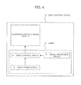
- FIG. 4 illustrates an example configuration of a light control device 12 having an SPD 8.
- the light control device 12 is provided with a drive 16 which includes the SPD 8, a drive control circuit 13 and a drive power supply 14 for driving the X-electrodes 3 and Y-electrodes 4 of the SPD 8, and a signal processing circuit 15 which processes input signals for controlling a light control area and the state of light control.
- the light control device 12 may be provided with an external signal input device for inputting an external environment information signal concerning, for example, incident light and temperature to the signal processing circuit 15.
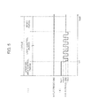
- FIG. 5 the composition of a driving cycle used in the driving method is shown in an upper part (I) and a corresponding driving waveform is shown in a lower part (II).
- the driving cycle is composed of an aperture area control period, a light control period, and a reset period.
- V DC l DC voltage
- V DC l DC electric field
- the X-electrode 3 and the Y-electrode 4 Since the light control particles 9 dispersed between the electrodes are negatively charged, they are localized on the Y-electrode 4 side.
- aperture width d1 shown in FIG. 8 can be controlled by adjusting t1 so as to determine a gray scale value.
- a driving waveform of voltage V AC l is applied to the Y-electrode 4 at a frequency of 50 to 1000 Hz in the light control period thereby forming an AC electric field between the X-electrode 3 and the Y-electrode 4.
- the light control particles 9 may move between the electrodes or their orientation may vary by being affected by the frequency of the AC electric field.
- the frequency of the AC electric field is, therefore, required to be high enough to keep the light control particles 9 oriented along the direction of the electric field between the electrodes.
- the frequency is desired to be not lower than the critical flicker frequency (CFF). It is preferably 15 Hz or higher.
- V AC l equals voltage V AC k which allows the light control particles 9 to be kept localized on the Y-electrode 4 side without returning into a dispersed state by Brownian motion.
- the degree of orientation of the light control particles 9 can be controlled by adjusting ARC voltage V AC l within the relationship of V AC k ⁇ V AC l ⁇ V AC h.
- the driving waveform to form the AC electric field may be a sine wave, rectangular wave (square wave) or triangular wave. Or, AC waveforms whose polarities alternate every half period may be simultaneously applied to the X-electrode 3 and the Y-electrode 4.
- FIGS. 6 to 11 illustrate the movement of the light control particles 9 and light control operations taking place in the SPD 8 when the driving method according to the present invention is used. Note that FIGS. 6 to 11 are sectional views showing one pair of X-electrode 3 and Y- electrode 4 out of those shown in FIG. 1 .
- FIG. 6 shows the SPD 8 in a state before being driven.
- the light control particles are almost uniformly dispersed, in an unregulated state, between the electrodes.
- incident light incident from behind is absorbed and blocked by the light control particles.
- FIG. 8 shows the SPD 8 in a state during the aperture area control period.
- the light control particles 9 being affected by the DC electric field are localized on the Y-electrode 4 side with almost no light control particles 9 located on the X-electrode 3 side.
- light 18 transmitted on the X-electrode 3 side shows high transmittance
- light 19 transmitted on the Y-electrode 4 side shows low transmittance.
- the aperture width d1 shown in FIG. 8 can be controlled by adjusting t1 shown in FIG. 5 .
- FIG. 10 shows the SPD 8 in a state during the light control period.
- the light control particles 9 are affected by AC voltage V AC l and are continuously changed from an unregulated state to a state in which they are oriented along the direction of the electric field.
- V AC l AC voltage
- FIG. 11 the state of transmission of incident light 17 changes, but light 20 transmitted on the Y-electrode 4 side shows a low transmittance with the state in which the light control particles 9 are localized on the Y-electrode 4 side maintained.
- the transmittance of the light 20 transmitted on the Y-electrode 4 side can be controlled by adjusting V AC l.
- the light control device 12 including the SPD of the present embodiment and using the driving method of the present embodiment can control optical properties between the electrodes. Namely, it can control an arbitrary low-transmittance area, i.e. a light blocking area, and an arbitrary high-transmittance area, i.e. a light transmitting area.
- AC voltage V AC l during the light control period is equal to or higher than V AC h, that is, high enough to cause the light control particles 9 to be adequately oriented, and the light control particles 9 are, as shown in FIGS. 10 and 11 , kept in a state in which they are affected by an AC electric field and oriented along the direction of the electric field. In that state, compared with a state in which the light control particles 9 are randomly arranged, some light leaks to outside. In such a state, there can be cases in which contrast cannot be secured. There is also a different aspect.
- a component orthogonal to the direction of the AC electric field of linearly polarized light can be outputted from an arbitrary area making use of the oriented light control particles.
- a suspended particle device has a structure which addresses the above problem and which can make use of the above feature.
- the SPD 8 is further provided with a polarizer 21 as shown in FIG. 12 .
- the driving method, and the drive 16, description already provided in connection with the first embodiment will be omitted in the following.
- FIG. 12 is a sectional view, like FIGS. 2A to 2C , in a y-z plane perpendicular to the driving electrode pairs and shows the SPD 8 and the polarizer 21 in an assembled state.
- the transparent supporting base is made of glass.
- the transparent supporting base may be made of a transparent resin film which preferably has, like glass, a low birefringence, for example, a sheet of cyclo-olefin polymer (COP).
- COP cyclo-olefin polymer
- the polarizer 21 is disposed on the SPD 8 with its absorption axis extending in parallel with the driving electrode pairs 5, that is, perpendicularly to the direction of the electric field.
- the polarizer 21 is a polarizing filter in which polyvinyl alcohol (PVA) contains a uniaxially oriented iodine complex and which is shaped like a sheet using, for example, triacetylcellulose (TAC).
- PVA polyvinyl alcohol
- TAC triacetylcellulose
- the polarizer 21 may also be a polarizing filter in which PVA contains not an iodine complex but a dichroism pigment. Or, the polarizer 21 may be replaced by a liquid crystal element provided with a drive.
- the driving cycle used in the driving method for the SPD 8 according to the present embodiment is, like in the first embodiment, composed of an aperture area control period, a light control period, and a reset period.
- FIGS, 13 and 14 illustrate the movement of light control particles and light control operations taking place in the SPD when the driving method according to the present embodiment is used.
- FIG. 13 shows the SPD 8 in a state during the light control period.
- the light control particles 9 are affected by the AC electric field and are kept in a state, changed to from an unregulated state, in which the light control particles 9 are oriented along the direction of the electric field. Therefore, in an area where the light control particles 8 are localized, when non-polarized light 22 enters the SPD 8 as shown in FIG. 14 , linearly-polarized light 23 is outputted from the SPD 8.
- the absorption axis of the poLarizer 21 disposed on the SPD 8 extends orthogonally to the direction of the electric field (driving electrode pairs). Hence, the linearly-polarized light 23 outputted from the SPD 8 is absorbed by the polarizer 21 disposed on the SPD 8. Namely, in the area where the light control particles 9 are localized, i.e. on the Y-electrode 4 side, the linearly-polarized light 23 is absorbed and blocked.
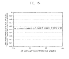
- FIG. 15 shows comparison between transmittance with a polarizer provided and transmittance with no polarizer provided.
- the vertical axis represents the ratio of the transmittance with a polarizer provided to the transmittance with no polarizer provided, i.e. (transmittance with a polarizer provided) / (transmittance with no polarizer provided).
- the ratio of light absorption depends on the transmittance of the polarizer 21, the concentration of the light control particles 9 used in the SPD 8 and the structure of the SPD 8. In the present embodiment, the transmittance is about half that observed when no polarizer is provided.
- the light control device 12 of the present embodiment using the SPD 8, the polarizer 21 and the driving method as described above can increase, as compared with the first embodiment, the difference in transmittance between a light blocking area and a light transmitting area, so that area control with a high contrast can be realized.
- the polarizer 21 is attached on the B-substrate 2 of the SPD 8, but the same effect can be obtained by attaching the polarizer 21 under the A-substrate.
- the polarizer 21 need not necessarily be attached to a substrate. It may be attached to an incident light source, which is separated from the SPD 8, for generating linearly-polarized light.
- the SPD as used in the first embodiment may be used as a polarizing SPD 25 to which an AC voltage VACh is applied and which is oriented to face the SPD 8 such that the driving electrode pairs 5 of the two SPDs extend to be mutually orthogonal as shown in FIG. 16 .
- the light control particles 9 are described as having optical anisotropy, the light control particles 9 does not necessarily have to be optically anisotropic. They may be, for example, charged spherical particles having prescribed charging characteristics. Namely, light control can be effected by applying a DC voltage across electrodes for a prescribed amount of time to localize the charged spherical particles and by subsequently applying an AC voltage to maintain the localized state of the particles.
- the light control device can be suitably used in various applications, for example: building materials such as indoor and outdoor partitions, window shades and window glasses/sky light windows for buildings; window materials for aircraft, automobiles, railroad vehicles and ships; electronic devices such as displays, optical shutters and polarizing devices; and optical devices such as glasses/sunglasses and mirrors.
- Plural light control devices according to the present invention may be combined for use, or such a light control device may be used in combination with a different device, for example, an LCD display.
Landscapes
- Physics & Mathematics (AREA)
- Nonlinear Science (AREA)
- General Physics & Mathematics (AREA)
- Optics & Photonics (AREA)
- Electrochromic Elements, Electrophoresis, Or Variable Reflection Or Absorption Elements (AREA)
Abstract
Description
- The present invention relates to a light control device in which a driving voltage is applied to particles present between electrodes and driving control performed therein and, particularly, to technology effectively applicable to a suspended particle device (hereinafter also referred to as an "SPD") .
- Great hopes are placed on light control devices using an SPD in the field of applications such as building materials aimed at energy saving through incident sunbeam control and display devices and optical devices using light transmission and reflection control functions. An SPD is a device whose optical characteristics vary between when no voltage is applied thereto and when a voltage is applied thereto. Generally, in an SPD, electrodes are formed on transparent substrates disposed to mutually face and a suspension containing light control particles (hereinafter also referred to simply as "particles") which are dispersed therein and which react to an electric field is provided between, the substrates and between the electrodes.
- The light control particles to be filled in an SPD are those which show optical anisotropy for absorption and reaction. Such light control particles include those which are caused to show optical anisotropy by their anisotropic shapes. Hence, particles whose aspect ratio is not 1 and which are rod-shaped, needle-shaped or shaped like flat plates are used as light control particles.
- When no voltage is applied, the light control particles in a suspension are engaged in Brownian motion to be oriented randomly, so that light incident on the suspension is absorbed and scattered to be blocked without being transmitted.
- When a voltage is applied, on the other hand, the light control particles in a suspension are affected by dielectric polarization caused by an electric field and are uniformly oriented along the direction of the electric field. In this state, light incident on the suspension is modulated by the oriented light control particles. According to Japanese Patent Laid-Open No.
Sho 53 (1978)-144893 - Another method for controlling a light control area in an SPD is disclosed in Japanese Patent Laid-Open No.
2005-156811 - When controlling a light control area using prior-art SPD technology, however, it is necessary to select an electrode pair across which a voltage is to be applied out of plural electrodes. For light-control area control, therefore, it is necessary to perform passive matrix drive or active matrix drive. Furthermore, to realize more continuous light-control area control, it is necessary to increase the number of electrodes. Increasing the number of electrodes, terminals and matrix drive elements makes the SPD structure more complicated resulting in increasing the number of production processes to eventually increase the production cost.
- Such a cost increase can be avoided by developing SPD technology which makes it possible to continuously control a light control area between electrodes. An object of the present invention is to provide technology for realizing light-control area control between electrodes by focusing attention on light control particle material, SPD structure, and SPD driving method.
- The present invention addresses the above problem mainly by the following means.
- (1) A suspended particle device includes a pair of substrates disposed to face each other with a suspension containing charged particles and a disperse medium filled therebetween and with an electrode pair formed on the suspension side of one of the pair of substrates. In the suspended particle device, light control is effected by applying a DC voltage across the electrode pair to localize the particles and subsequently applying an AC voltage across the electrode pair to maintain the localized state of the localized particles. In the suspended particle device, the charged particles preferably have optical anisotropy.
- (2) A suspended particle device includes a pair of substrates disposed to face each other with a suspension charged particles and a disperse medium filled therebetween and with an electrode pair formed on the suspension side of one of the pair of substrates. In the suspended particle device: the charged particles have optical anisotropy; an outer side of one of the pair of substrates is attached with a polarizer; and light control is effected by applying a DC voltage across the electrode pair to localize the charged particles and subsequently applying an AC voltage across the electrode pair to maintain the localized state of the localized charged particles. In the suspended particle device, it is preferable that; in a state with the AC voltage applied, the suspension in an area where the charged particles are localized has a polarization effect with an absorption axis thereof aligned in a. prescribed direction; and the absorption axis of the suspension and an absorption axis of the polarizer are orthogonal to each other.
- According to the present invention, a light control area can be controlled without requiring any complicated switching circuit to be formed on a substrate, so that a light control device having a simple structure and being capable of controlling a light control area can be realized.
-
-
FIG. 1 is an exploded perspective view schematically showing a principal portion of a suspended particle device (SPD) according to the present invention; -
FIGS. 2A to 2C are sectional views in a y-z plane showing a portion including a driving electrode pair of the SPD shown inFIG. 1 ,FIG. 2A showing a state with no voltage applied,FIG. 2B showing a state with a medium AC voltage applied andFIG. 2C showing a state with a high AC voltage applied; -
FIG. 3 is a graph showing variation in transmittance with respect to AC voltage VACl in the SPD shown inFIG. 1 ; -
FIG. 4 illustrates a configuration of a light control device using the SPD shown inFIG. 1 ; -
FIG. 5 illustrates the composition of a driving method for controlling a light control area in the SPD shown inFIG. 1 and a corresponding driving waveform; -
FIG. 6 is a diagram showing an internal state of an SPD according to a first embodiment before being driven; -
FIG. 7 is a diagram showing the optical path of incident light on the SPD of the first embodiment before being driven; -
FIG. 8 is a diagram showing an internal state of the SPD of the first embodiment during an aperture area control period; -
FIG. 9 is a diagram showing the optical path of incident light on the SPD of the first embodiment during the aperture area control period; -
FIG. 10 is a diagram showing an internal state of the SPD of the first embodiment during a light control period; -
FIG. 11 is a diagram showing the optical path of incident light on the SPD of the first embodiment during the light control period; -
FIG. 12 shows, based on a y-z plane sectional view of an electrode pair shown inFIG. 1 , an essential portion of an SPD according to a second embodiment; -
FIG. 13 is a diagram showing an internal state of the SPD of the second embodiment during a light control period; -
FIG. 14 is a diagram showing the optical path of incident light on the SPD of the second embodiment during the light control period; -
FIG. 15 is a graph showing the ratio between transmittance with a provides and transmittance with no polarizer provided in the SPD of the second embodiment; and -
FIG. 16 is an exploded perspective view showing a structure of a light control device including the SPD of the second embodiment in which the SPD of the first embodiment is used as a polarizer. - Embodiments will be described in detail below with reference to drawings. Note that, in all the drawings referred to in describing the following embodiments, components having identical functions are assigned identical reference symbols and duplication of their description may be avoided.
- First, to make the present invention easier to understand, the basic structure of a suspected particle device (SPD) studied by the present inventors will be described. Note that, of the two substrates disposed to face each other in the SPD, the one provided with electrode pairs to form electric fields in a suspension filled between the substrates is referred to as an "A-plate" and the other provided with no electrode pairs is referred to as a "B-plate." In the present application, the A-plate and B-plate are described as an A-substrate and B-substrate, respectively, each formed of a transparent sheet-like supporting base of, for example, a resin film such as polyethylene terephthalate (PET), polycarbonate (PC), or cyclo-olefin polymer (COP) or glass.
-
FIG. 1 is an exploded perspective view schematically showing a principal portion of the SPD studied by the present inventors.FIGS. 2A to 2C are sectional views in a y-z plane showing a portion including a pair of driving electrodes of the SPD in an assembled state. In the following, first an A-plate denoted inFIG. 1 byreference numeral 6 will be described including how it is formed. Referring toFIG. 1 , pluraldriving electrode pairs 5 each comprised of anX-electrode 3 and a Y-electrode 4 are arranged in a stripe pattern on theA-substrate 1. The X-electrodes 3 and Y-electrodes 4 are successively alternately arranged along a lateral direction. The X-electrodes 3 and Y-electrodes 4 each have a width of, for example, 10 µm and the distance between each pair ofX-electrode 3 and Y-electrode 4 is, for example, 15 µm. Note that these dimensions may largely differ depending on applications. In the present example, the voltage to drive the X-electrode 3 and Y-electrode 4, being described later, is several tens of volts (effective value). - The driving
electrode pairs 5 are transparent electrodes formed of indium tin oxide (ITO) which is a transparent conductor. The drivingelectrode pairs 5 may also be formed of a transparent such as tin oxide or zinc oxide or a metallic single-layer or multi-layer film, for example, of chrome. Even though, in the present embodiment, the driving electrodes are arranged in a stripe pattern, they may be arranged differently, for example, in a circular pattern or in a pattern of a letter. - Next, the A-plate and B-plate are disposed to face each other, sealant containing spacer beads is applied to mutually facing portions along the edges (not shown) of the two plates, and the two plates are bonded together thereby forming a space to be filled with a suspension (hereinafter also referred to as a "suspension space"). The suspension space may be maintained by spraying the spacer beads between the two plates. In cases where the X-electrodes 3 and Y-
electrodes 4 each have a width of about 10 µm and the distance between each pair ofX-electrode 3 and Y-electrode 4 is about 15 µm, the thickness of the suspension space is, for example, 20 µm or less. - A
suspension 11 used in the present embodiment contains light control particles 9 and a dispersemedium 10. The light control particles 9 are anisotropically shaped and display optical anisotropy with varied absorbance attributable to their orientation. The aspect ratio of their shape is other than 1 and they are negatively charged. The light control particles 9 have, for example, a rod-like shape with a long-axis length of several hundred nm and an aspect ratio of, for example, 5 to 30. The light control particles 9 may be formed of a carbon-based material such as polyperiodides or carbon black, a metallic material such as copper, nickel, iron, cobalt, chrome, titanium, or aluminum, or particles of an inorganic compound, for example, silicon nitride or titanium nitride. They are charged positively or negatively. Materials such as carbon black and metals are not charged to a specific polarity themselves, but they can be charged as prescribed by being coated with material having property of being charged to a specific polarity. - The disperse medium 10 contained in the
suspension 11 is a liquid copolymer of a (meth) acrylic acid ester oligomer. Preferably, the dispersemedium 10 has a viscosity which allows the light control particles 9 to be suspended, fluid and movable, has a high resistance, is affinitive with neither the supporting base nor the driving electrodes, has a reflective index close to that of the supporting base, and has a permittivity different from that of the light control particles. A difference in reflective index between the dispersemedium 10 and the light control particles 9 can be utilized, in orienting the light control particles 9 as being described later, as a driving force in an AC electric field. In the present embodiment, the specific permittivity of the dispersemedium 10 is 4 to 5. - The
suspension 11 is filled in the suspension space through end portions left unbonded by sealant of both plates by making use of capillary action. After thesuspension 11 is filled between the two plates, the unbonded end portions of the two plates are sealed by bonding them together using a sealant. This isolates thesuspension 11 from outside air. -
FIG. 3 shows variation in transmittance of light transmitted from the A-substrate 1 side: to the B-substrate 2 side with respect to AC voltage VACl applied across the X-electrode 3 and the Y-electrode 4. When no voltage is applied across the X-electrode 3 and the Y-electrode 4 (VAcl = 0), the light control particles 9 are, as shown inFIG. 2A , randomly oriented to absorb and scatter light, so that transmittance is low. - When an AC voltage VACl is applied across the X-electrode 3 and the Y-
electrode 4, as shown inFIG. 2B , the degree of orientation of the light control particles 9 along the direction of the electric field increases. This causes the amount of light transmitted through clearances between the light control particles 9 to increase resulting in an increased transmittance where AC voltage VACl = VACm. - When an adequately high AC voltage VACh is applied across the X-electrode 3 and the Y-
electrode 4, the light control particles 9 are, as shown inFIG. 2C , almost entirely oriented along the direction of the electric field. Where AC voltage VACl is VACh or higher, the light control particles 9 are adequately oriented along the direction of the electric field, so that the transmittance does not increase much. -
FIG. 4 illustrates an example configuration of alight control device 12 having anSPD 8. Thelight control device 12 is provided with a drive 16 which includes theSPD 8, adrive control circuit 13 and adrive power supply 14 for driving the X-electrodes 3 and Y-electrodes 4 of theSPD 8, and asignal processing circuit 15 which processes input signals for controlling a light control area and the state of light control. Thelight control device 12 may be provided with an external signal input device for inputting an external environment information signal concerning, for example, incident light and temperature to thesignal processing circuit 15. - Next, the driving method used in the present embodiment will be described. In
FIG. 5 , the composition of a driving cycle used in the driving method is shown in an upper part (I) and a corresponding driving waveform is shown in a lower part (II). The driving cycle is composed of an aperture area control period, a light control period, and a reset period. In the aperture area control period, DC voltage VDCl is applied to the Y-electrode 4 and a DC electric field is formed between the X-electrode 3 and the Y-electrode 4. Since the light control particles 9 dispersed between the electrodes are negatively charged, they are localized on the Y-electrode 4 side. - At this time, by adjusting DC voltage VDCl, electric field EDCl formed between the electrodes, and DC electric field formation time t1, it is possible to localize the light control particles 9 in a desired area on the Y-
electrode 4 side. Namely, aperture width d1 shown inFIG. 8 can be controlled by adjusting t1 so as to determine a gray scale value. - After localizing the light control particles 9 in a desired area on the Y-
electrode 4 side, a driving waveform of voltage VACl is applied to the Y-electrode 4 at a frequency of 50 to 1000 Hz in the light control period thereby forming an AC electric field between the X-electrode 3 and the Y-electrode 4. This causes the light control particles 9 localized on the Y-electrode 4 side to be retained where they are in a state of being oriented along the direction of the electric field. In cases where the frequency of the AC electric field is extremely low, the light control particles 9 may move between the electrodes or their orientation may vary by being affected by the frequency of the AC electric field. The frequency of the AC electric field is, therefore, required to be high enough to keep the light control particles 9 oriented along the direction of the electric field between the electrodes. Hence, the frequency is desired to be not lower than the critical flicker frequency (CFF). It is preferably 15 Hz or higher. - VACl equals voltage VACk which allows the light control particles 9 to be kept localized on the Y-
electrode 4 side without returning into a dispersed state by Brownian motion. The degree of orientation of the light control particles 9 can be controlled by adjusting ARC voltage VACl within the relationship of VACk ≤ VACl ≤ VACh. The driving waveform to form the AC electric field may be a sine wave, rectangular wave (square wave) or triangular wave. Or, AC waveforms whose polarities alternate every half period may be simultaneously applied to the X-electrode 3 and the Y-electrode 4. - In the reset period according to the driving method of the present embodiment, voltage application to the electrodes is discontinued to bring the light control particles 9 localized on the Y-
electrode 4 side in a state of being oriented along the direction of the electric field back into a dispersed state between the electrodes. Referring toFIG. 5 , even though DC voltage VDCl in the aperture area control period is higher in absolute value than the wave height value VACl of the AC voltage in the light control period, it only represents an example and there can be cases where DC voltage VDCl is smaller than the wave height value VACl of the AC voltage. The magnitude of DC voltage VDCl is determined taking into consideration DC electric field formation time t1. -
FIGS. 6 to 11 illustrate the movement of the light control particles 9 and light control operations taking place in theSPD 8 when the driving method according to the present invention is used. Note thatFIGS. 6 to 11 are sectional views showing one pair ofX-electrode 3 and Y-electrode 4 out of those shown inFIG. 1 . -
FIG. 6 shows theSPD 8 in a state before being driven. As shown, the light control particles are almost uniformly dispersed, in an unregulated state, between the electrodes. As shown inFIG. 7 , incident light incident from behind is absorbed and blocked by the light control particles. -
FIG. 8 shows theSPD 8 in a state during the aperture area control period. As shown, the light control particles 9 being affected by the DC electric field are localized on the Y-electrode 4 side with almost no light control particles 9 located on the X-electrode 3 side. Hence, as shown inFIG. 9 , light 18 transmitted on the X-electrode 3 side shows high transmittance whereas light 19 transmitted on the Y-electrode 4 side shows low transmittance. The aperture width d1 shown inFIG. 8 can be controlled by adjusting t1 shown inFIG. 5 . -
FIG. 10 shows theSPD 8 in a state during the light control period. The light control particles 9 are affected by AC voltage VACl and are continuously changed from an unregulated state to a state in which they are oriented along the direction of the electric field. At this time, as shown inFIG. 11 , the state of transmission of incident light 17 changes, but light 20 transmitted on the Y-electrode 4 side shows a low transmittance with the state in which the light control particles 9 are localized on the Y-electrode 4 side maintained. The transmittance of the light 20 transmitted on the Y-electrode 4 side can be controlled by adjusting VACl. - Thus, the
light control device 12 including the SPD of the present embodiment and using the driving method of the present embodiment can control optical properties between the electrodes. Namely, it can control an arbitrary low-transmittance area, i.e. a light blocking area, and an arbitrary high-transmittance area, i.e. a light transmitting area. - In the light control device of the first embodiment, AC voltage VACl during the light control period is equal to or higher than VACh, that is, high enough to cause the light control particles 9 to be adequately oriented, and the light control particles 9 are, as shown in
FIGS. 10 and11 , kept in a state in which they are affected by an AC electric field and oriented along the direction of the electric field. In that state, compared with a state in which the light control particles 9 are randomly arranged, some light leaks to outside. In such a state, there can be cases in which contrast cannot be secured. There is also a different aspect. Namely, in an area where the light control particles are localized, when non-polarized light enters the SPD, a component orthogonal to the direction of the AC electric field of linearly polarized light can be outputted from an arbitrary area making use of the oriented light control particles. - A suspended particle device according to a second embodiment of the present invention has a structure which addresses the above problem and which can make use of the above feature. According to the second embodiment, the
SPD 8 is further provided with apolarizer 21 as shown inFIG. 12 . As for theSPD 8, the driving method, and the drive 16, description already provided in connection with the first embodiment will be omitted in the following. -
FIG. 12 is a sectional view, likeFIGS. 2A to 2C , in a y-z plane perpendicular to the driving electrode pairs and shows theSPD 8 and thepolarizer 21 in an assembled state. In the present embodiment, the transparent supporting base is made of glass. The transparent supporting base may be made of a transparent resin film which preferably has, like glass, a low birefringence, for example, a sheet of cyclo-olefin polymer (COP). - The
polarizer 21 is disposed on theSPD 8 with its absorption axis extending in parallel with the driving electrode pairs 5, that is, perpendicularly to the direction of the electric field. Thepolarizer 21 is a polarizing filter in which polyvinyl alcohol (PVA) contains a uniaxially oriented iodine complex and which is shaped like a sheet using, for example, triacetylcellulose (TAC). Thepolarizer 21 may also be a polarizing filter in which PVA contains not an iodine complex but a dichroism pigment. Or, thepolarizer 21 may be replaced by a liquid crystal element provided with a drive. - The driving cycle used in the driving method for the
SPD 8 according to the present embodiment is, like in the first embodiment, composed of an aperture area control period, a light control period, and a reset period.FIGS, 13 and14 illustrate the movement of light control particles and light control operations taking place in the SPD when the driving method according to the present embodiment is used. -
FIG. 13 shows theSPD 8 in a state during the light control period. As shown, the light control particles 9 are affected by the AC electric field and are kept in a state, changed to from an unregulated state, in which the light control particles 9 are oriented along the direction of the electric field. Therefore, in an area where thelight control particles 8 are localized, whennon-polarized light 22 enters theSPD 8 as shown inFIG. 14 , linearly-polarizedlight 23 is outputted from theSPD 8. The absorption axis of thepoLarizer 21 disposed on theSPD 8 extends orthogonally to the direction of the electric field (driving electrode pairs). Hence, the linearly-polarizedlight 23 outputted from theSPD 8 is absorbed by thepolarizer 21 disposed on theSPD 8. Namely, in the area where the light control particles 9 are localized, i.e. on the Y-electrode 4 side, the linearly-polarizedlight 23 is absorbed and blocked. -
FIG. 15 shows comparison between transmittance with a polarizer provided and transmittance with no polarizer provided. Namely, inFIG. 15 , the vertical axis represents the ratio of the transmittance with a polarizer provided to the transmittance with no polarizer provided, i.e. (transmittance with a polarizer provided) / (transmittance with no polarizer provided). The ratio of light absorption depends on the transmittance of thepolarizer 21, the concentration of the light control particles 9 used in theSPD 8 and the structure of theSPD 8. In the present embodiment, the transmittance is about half that observed when no polarizer is provided. In the present embodiment, there are almost no light control particles 9 on the X-electrode 3 side, so that, even though light 24 transmitted on the X-electrode 3 side causes linearly polarized light to be generated at thepolarizer 21, the transmittance is extremely higher on the X-electrode 3 side than on the Y-electrode 4 side. - Thus, the
light control device 12 of the present embodiment using theSPD 8, thepolarizer 21 and the driving method as described above can increase, as compared with the first embodiment, the difference in transmittance between a light blocking area and a light transmitting area, so that area control with a high contrast can be realized. - Referring to
FIG. 12 , thepolarizer 21 is attached on the B-substrate 2 of theSPD 8, but the same effect can be obtained by attaching thepolarizer 21 under the A-substrate. Thepolarizer 21 need not necessarily be attached to a substrate. It may be attached to an incident light source, which is separated from theSPD 8, for generating linearly-polarized light. Also, instead of using the polarizer, the SPD as used in the first embodiment may be used as apolarizing SPD 25 to which an AC voltage VACh is applied and which is oriented to face theSPD 8 such that the drivingelectrode pairs 5 of the two SPDs extend to be mutually orthogonal as shown inFIG. 16 . - Description has been provided above in terms of one pair of
X-electrode 3 and Y-electrode 4, but similar effects can also be obtained using plural pairs ofX-electrodes 3 and Y-electrodes 4 arranged in parallel. Namely, using many pairs ofX-electrodes 3 and Y-electrodes 4 arranged in parallel makes light control over a wider area possible. - Even though, in the foregoing, the light control particles 9 are described as having optical anisotropy, the light control particles 9 does not necessarily have to be optically anisotropic. They may be, for example, charged spherical particles having prescribed charging characteristics. Namely, light control can be effected by applying a DC voltage across electrodes for a prescribed amount of time to localize the charged spherical particles and by subsequently applying an AC voltage to maintain the localized state of the particles.
- The light control device according to the present invention can be suitably used in various applications, for example: building materials such as indoor and outdoor partitions, window shades and window glasses/sky light windows for buildings; window materials for aircraft, automobiles, railroad vehicles and ships; electronic devices such as displays, optical shutters and polarizing devices; and optical devices such as glasses/sunglasses and mirrors. Plural light control devices according to the present invention may be combined for use, or such a light control device may be used in combination with a different device, for example, an LCD display.
- The above embodiments of the invention as well as the appended claims and figures show multiple characterizing features of the invention in specific combinations. The skilled person will easily be able to consider further combinations or sub-combinations of these features in order to adapt the invention as defined in the in the claims to his specific needs.
Claims (11)
- A suspended particle device comprising a pair of substrates (1, 2) disposed to face each other with a suspension containing charged particles (9) and a disperse medium (10) filled therebetween and with an electrode pair (3, 4) formed on the suspension side of one of the pair of substrates (1)
wherein the device comprises means for effecting light control by applying a DC voltage across the electrode pair (3, 4) to localize the particles (9) and by subsequently applying an AC voltage across the electrode pair (3, 4) to maintain the localized state of the localized particles (9). - The suspended particle device according to claim 1, wherein the charged particles (9) have optical anisotropy.
- The suspended particle device according to claim 1, wherein the charged particles (9) and the disperse medium (10) differ in specific permittivity.
- The suspended particle device according to claim 1, wherein the charged particles (9): are rod-shaped and have an aspect ratio in a range of 5 to 30.
- The suspended particle device according to claim 1, wherein, when an AC voltage is applied across the electrode pair (3, 4), light incident on the suspension is polarized by the charged particles (9).
- A suspended particle device according to claim 2, wherein an outer side of one of the pair of substrates is attached with a polarizer (21).
- The suspended particle device according to claim 6, wherein, in a state with the AC voltage applied, the suspension in an area where the charged particles (9) are localized has a polarization effect with an absorption axis thereof aligned in a prescribed direction, and the absorption axis of the suspension and an absorption axis of the polarizer (21) are orthogonal to each other.
- The suspended particle device according to one of the preceding claims, wherein a frequency of the AC voltage is 16 Hz or higher.
- A method for driving a suspended particle device which includes a pair of substrates (1, 2) disposed to face each other with a suspension containing charged particles (9) and a disperse medium (10) filled therebetween and with an electrode pair (3, 4) formed on the suspension side of one on the pair of substrates (1, 2), the method comprising:an aperture area control period for localizing the particles (9) by applying a DC voltage across the electrode pair(3, 4);a light control period for maintaining a localized state of the localized particles (9) by applying, after the aperture area control period, an AC voltage across the electrode pair (3, 4); anda reset period which follows the light control period and during which the voltage applied, in the light control period, across the electrode pair (3, 4) is kept removed.
- A method for driving a suspended particle device according to claim 9, the charged particles (9) having optical anisotropy and a disperse medium (10) filled therebetween, wherein a polarizer (21) is attached to an outer side of one of the pair of substrates (1, 2).
- The method for driving a suspended particle device according to claim 9 or 10, wherein a frequency of the AC voltage is 16 Hz or higher.
Applications Claiming Priority (1)
| Application Number | Priority Date | Filing Date | Title |
|---|---|---|---|
| JP2010167290A JP5423603B2 (en) | 2010-07-26 | 2010-07-26 | Suspended particle device and driving method thereof |
Publications (2)
| Publication Number | Publication Date |
|---|---|
| EP2413184A1 true EP2413184A1 (en) | 2012-02-01 |
| EP2413184B1 EP2413184B1 (en) | 2014-01-29 |
Family
ID=44514531
Family Applications (1)
| Application Number | Title | Priority Date | Filing Date |
|---|---|---|---|
| EP11175469.3A Not-in-force EP2413184B1 (en) | 2010-07-26 | 2011-07-26 | Suspended particle device and method for driving same |
Country Status (3)
| Country | Link |
|---|---|
| US (1) | US8599470B2 (en) |
| EP (1) | EP2413184B1 (en) |
| JP (1) | JP5423603B2 (en) |
Cited By (2)
| Publication number | Priority date | Publication date | Assignee | Title |
|---|---|---|---|---|
| EP2648038A1 (en) * | 2012-04-03 | 2013-10-09 | Hitachi Chemical Company, Ltd. | Light control device |
| WO2020186649A1 (en) * | 2019-03-20 | 2020-09-24 | Boe Technology Group Co., Ltd. | Display panel, control methods thereof, and display device |
Families Citing this family (7)
| Publication number | Priority date | Publication date | Assignee | Title |
|---|---|---|---|---|
| JP5556762B2 (en) * | 2011-08-01 | 2014-07-23 | 日立化成株式会社 | Suspended particle device, light control device using suspended particle device, and driving method thereof |
| JP5516616B2 (en) * | 2012-02-07 | 2014-06-11 | 日立化成株式会社 | Suspended particle device, light control device using the same, and driving method thereof |
| JP5900233B2 (en) * | 2012-08-08 | 2016-04-06 | 日立化成株式会社 | Light control element, light control device, and driving method thereof |
| US9658491B2 (en) * | 2013-04-24 | 2017-05-23 | Sharp Kabushiki Kaisha | Optical apparatus and display apparatus provided with same |
| US10310298B2 (en) * | 2016-10-25 | 2019-06-04 | GM Global Technology Operations LLC | Smart sensor-cover apparatus and methods and computer products for implementing same |
| CN114839760A (en) * | 2022-05-06 | 2022-08-02 | 深圳市华科创智技术有限公司 | Light valve and preparation method thereof |
| CN119717356A (en) * | 2025-01-21 | 2025-03-28 | 浙江精一新材料科技有限公司 | Dimming film and dimming glass |
Citations (6)
| Publication number | Priority date | Publication date | Assignee | Title |
|---|---|---|---|---|
| JPS53144893A (en) | 1977-05-23 | 1978-12-16 | Research Frontiers Inc | Polarizing material and manufacture thereof |
| US4442019A (en) * | 1978-05-26 | 1984-04-10 | Marks Alvin M | Electroordered dipole suspension |
| JP2005156811A (en) | 2003-11-25 | 2005-06-16 | Fuji Photo Film Co Ltd | Display device |
| US20050185104A1 (en) * | 2002-07-25 | 2005-08-25 | Genewave | Optically active glazing |
| US20050190431A1 (en) * | 2004-01-27 | 2005-09-01 | Canon Kabushiki Kaisha | Display apparatus and driving method thereof |
| US20070164983A1 (en) * | 2006-01-06 | 2007-07-19 | Canon Kabushiki Kaisha | Electrophoretic display apparatus |
Family Cites Families (16)
| Publication number | Priority date | Publication date | Assignee | Title |
|---|---|---|---|---|
| JPH0519306A (en) * | 1991-07-16 | 1993-01-29 | Nippon Sheet Glass Co Ltd | Fully solid-state dimming device and dimming method with the same |
| JP4460150B2 (en) * | 1997-08-28 | 2010-05-12 | イー インク コーポレイション | A new addressing scheme for electrophoretic displays. |
| KR100575452B1 (en) * | 1999-09-28 | 2006-05-03 | 엘지.필립스 엘시디 주식회사 | Reflective type liquid crystal display using electrophoretic display and electrophoretic display |
| JP4532938B2 (en) * | 2003-03-04 | 2010-08-25 | キヤノン株式会社 | Electrophoretic display device and driving method thereof |
| JP4076222B2 (en) * | 2003-07-25 | 2008-04-16 | 株式会社東芝 | Electrophoretic display device |
| JP4522101B2 (en) * | 2004-01-27 | 2010-08-11 | キヤノン株式会社 | Electrophoretic display device and driving method of electrophoretic display device |
| EP1779174A4 (en) * | 2004-07-27 | 2010-05-05 | E Ink Corp | Electro-optic displays |
| JP2007114622A (en) * | 2005-10-21 | 2007-05-10 | Canon Inc | Particle movement type display device and driving method thereof |
| JPWO2008012934A1 (en) * | 2006-07-24 | 2009-12-17 | 太田 勲夫 | Display device and manufacturing method thereof |
| JP4049202B1 (en) * | 2006-11-10 | 2008-02-20 | 富士ゼロックス株式会社 | Display medium, display device, and display method |
| WO2008075774A1 (en) | 2006-12-21 | 2008-06-26 | Hitachi Chemical Co., Ltd. | Light control film |
| WO2008075773A1 (en) | 2006-12-21 | 2008-06-26 | Hitachi Chemical Co., Ltd. | Light control film and light control glass |
| JP2008158041A (en) * | 2006-12-21 | 2008-07-10 | Hitachi Chem Co Ltd | Light control material, light control film and method for manufacturing light control film |
| EP2124097A4 (en) | 2006-12-21 | 2010-09-08 | Hitachi Chemical Co Ltd | FILM AND GLASS ANTI-REFLECTION |
| JP5321470B2 (en) | 2008-01-23 | 2013-10-23 | 日立化成株式会社 | Light control film |
| US8817360B2 (en) | 2008-03-05 | 2014-08-26 | Hitachi Chemical Company, Ltd. | Method for producing light-modulating film and light-modulating film |
-
2010
- 2010-07-26 JP JP2010167290A patent/JP5423603B2/en not_active Expired - Fee Related
-
2011
- 2011-07-25 US US13/189,626 patent/US8599470B2/en not_active Expired - Fee Related
- 2011-07-26 EP EP11175469.3A patent/EP2413184B1/en not_active Not-in-force
Patent Citations (6)
| Publication number | Priority date | Publication date | Assignee | Title |
|---|---|---|---|---|
| JPS53144893A (en) | 1977-05-23 | 1978-12-16 | Research Frontiers Inc | Polarizing material and manufacture thereof |
| US4442019A (en) * | 1978-05-26 | 1984-04-10 | Marks Alvin M | Electroordered dipole suspension |
| US20050185104A1 (en) * | 2002-07-25 | 2005-08-25 | Genewave | Optically active glazing |
| JP2005156811A (en) | 2003-11-25 | 2005-06-16 | Fuji Photo Film Co Ltd | Display device |
| US20050190431A1 (en) * | 2004-01-27 | 2005-09-01 | Canon Kabushiki Kaisha | Display apparatus and driving method thereof |
| US20070164983A1 (en) * | 2006-01-06 | 2007-07-19 | Canon Kabushiki Kaisha | Electrophoretic display apparatus |
Cited By (3)
| Publication number | Priority date | Publication date | Assignee | Title |
|---|---|---|---|---|
| EP2648038A1 (en) * | 2012-04-03 | 2013-10-09 | Hitachi Chemical Company, Ltd. | Light control device |
| WO2020186649A1 (en) * | 2019-03-20 | 2020-09-24 | Boe Technology Group Co., Ltd. | Display panel, control methods thereof, and display device |
| US11822203B2 (en) | 2019-03-20 | 2023-11-21 | Beijing Boe Optoelectronics Technology Co., Ltd. | Display panel, control methods thereof, and display device |
Also Published As
| Publication number | Publication date |
|---|---|
| US8599470B2 (en) | 2013-12-03 |
| JP2012027326A (en) | 2012-02-09 |
| EP2413184B1 (en) | 2014-01-29 |
| JP5423603B2 (en) | 2014-02-19 |
| US20120019897A1 (en) | 2012-01-26 |
Similar Documents
| Publication | Publication Date | Title |
|---|---|---|
| EP2413184B1 (en) | Suspended particle device and method for driving same | |
| CN106660003B (en) | Two-particle total internal reflection image display | |
| EP2555049B1 (en) | Suspended particle device, light control device using the same, and method for driving the same | |
| JP5454519B2 (en) | Light control element | |
| JP5516616B2 (en) | Suspended particle device, light control device using the same, and driving method thereof | |
| CN205176423U (en) | Liquid crystal display module with peep -proof and electromagnetic shielding function | |
| JP6425080B2 (en) | Optical device | |
| CN108027470A (en) | Optical film | |
| CN111465892B (en) | Liquid crystal cell | |
| CN111886537A (en) | Method, system and apparatus for reflection-emission hybrid display | |
| CN103293738A (en) | Liquid crystal display device and control method thereof | |
| WO2013141051A1 (en) | Display panel and display device | |
| CN110596934A (en) | Liquid crystal display panel and driving method | |
| WO2019071267A1 (en) | Method, apparatus and system for totally internally reflected high gain liquid crystal display | |
| CN210488182U (en) | Intelligent glass and display device | |
| KR20140024642A (en) | Transparent display with excellent visibility using pdlc film | |
| JPS6127725B2 (en) | ||
| JP2017021124A (en) | Dimmer and dimming plate | |
| KR102126748B1 (en) | Front/Rear Projection Type Smart Screen Apparatus Comprising Nano-Particle Layer | |
| KR102718025B1 (en) | Viewing angle variable element and display assembly | |
| CN113454523B (en) | Dimmers, dimming devices and management methods of dimming slices | |
| JP4826714B2 (en) | Electronic paper | |
| CN215770449U (en) | Counter glass projection display device | |
| JP7707688B2 (en) | Light-adjusting sheet | |
| RU2081443C1 (en) | Liquid-crystal device |
Legal Events
| Date | Code | Title | Description |
|---|---|---|---|
| 17P | Request for examination filed |
Effective date: 20111115 |
|
| AK | Designated contracting states |
Kind code of ref document: A1 Designated state(s): AL AT BE BG CH CY CZ DE DK EE ES FI FR GB GR HR HU IE IS IT LI LT LU LV MC MK MT NL NO PL PT RO RS SE SI SK SM TR |
|
| AX | Request for extension of the european patent |
Extension state: BA ME |
|
| PUAI | Public reference made under article 153(3) epc to a published international application that has entered the european phase |
Free format text: ORIGINAL CODE: 0009012 |
|
| GRAP | Despatch of communication of intention to grant a patent |
Free format text: ORIGINAL CODE: EPIDOSNIGR1 |
|
| RIC1 | Information provided on ipc code assigned before grant |
Ipc: G02F 1/167 20060101ALI20121010BHEP Ipc: G02F 1/17 20060101AFI20121010BHEP Ipc: G09G 3/34 20060101ALI20121010BHEP |
|
| 17Q | First examination report despatched |
Effective date: 20130408 |
|
| GRAP | Despatch of communication of intention to grant a patent |
Free format text: ORIGINAL CODE: EPIDOSNIGR1 |
|
| INTG | Intention to grant announced |
Effective date: 20130927 |
|
| GRAS | Grant fee paid |
Free format text: ORIGINAL CODE: EPIDOSNIGR3 |
|
| GRAA | (expected) grant |
Free format text: ORIGINAL CODE: 0009210 |
|
| AK | Designated contracting states |
Kind code of ref document: B1 Designated state(s): AL AT BE BG CH CY CZ DE DK EE ES FI FR GB GR HR HU IE IS IT LI LT LU LV MC MK MT NL NO PL PT RO RS SE SI SK SM TR |
|
| REG | Reference to a national code |
Ref country code: GB Ref legal event code: FG4D |
|
| REG | Reference to a national code |
Ref country code: CH Ref legal event code: EP |
|
| REG | Reference to a national code |
Ref country code: AT Ref legal event code: REF Ref document number: 651632 Country of ref document: AT Kind code of ref document: T Effective date: 20140215 |
|
| REG | Reference to a national code |
Ref country code: IE Ref legal event code: FG4D |
|
| REG | Reference to a national code |
Ref country code: DE Ref legal event code: R096 Ref document number: 602011004853 Country of ref document: DE Effective date: 20140313 |
|
| REG | Reference to a national code |
Ref country code: AT Ref legal event code: MK05 Ref document number: 651632 Country of ref document: AT Kind code of ref document: T Effective date: 20140129 |
|
| REG | Reference to a national code |
Ref country code: NL Ref legal event code: VDEP Effective date: 20140129 |
|
| REG | Reference to a national code |
Ref country code: LT Ref legal event code: MG4D |
|
| PG25 | Lapsed in a contracting state [announced via postgrant information from national office to epo] |
Ref country code: IS Free format text: LAPSE BECAUSE OF FAILURE TO SUBMIT A TRANSLATION OF THE DESCRIPTION OR TO PAY THE FEE WITHIN THE PRESCRIBED TIME-LIMIT Effective date: 20140529 Ref country code: LT Free format text: LAPSE BECAUSE OF FAILURE TO SUBMIT A TRANSLATION OF THE DESCRIPTION OR TO PAY THE FEE WITHIN THE PRESCRIBED TIME-LIMIT Effective date: 20140129 Ref country code: NO Free format text: LAPSE BECAUSE OF FAILURE TO SUBMIT A TRANSLATION OF THE DESCRIPTION OR TO PAY THE FEE WITHIN THE PRESCRIBED TIME-LIMIT Effective date: 20140429 |
|
| PG25 | Lapsed in a contracting state [announced via postgrant information from national office to epo] |
Ref country code: NL Free format text: LAPSE BECAUSE OF FAILURE TO SUBMIT A TRANSLATION OF THE DESCRIPTION OR TO PAY THE FEE WITHIN THE PRESCRIBED TIME-LIMIT Effective date: 20140129 Ref country code: CY Free format text: LAPSE BECAUSE OF FAILURE TO SUBMIT A TRANSLATION OF THE DESCRIPTION OR TO PAY THE FEE WITHIN THE PRESCRIBED TIME-LIMIT Effective date: 20140129 Ref country code: PT Free format text: LAPSE BECAUSE OF FAILURE TO SUBMIT A TRANSLATION OF THE DESCRIPTION OR TO PAY THE FEE WITHIN THE PRESCRIBED TIME-LIMIT Effective date: 20140529 Ref country code: ES Free format text: LAPSE BECAUSE OF FAILURE TO SUBMIT A TRANSLATION OF THE DESCRIPTION OR TO PAY THE FEE WITHIN THE PRESCRIBED TIME-LIMIT Effective date: 20140129 Ref country code: AT Free format text: LAPSE BECAUSE OF FAILURE TO SUBMIT A TRANSLATION OF THE DESCRIPTION OR TO PAY THE FEE WITHIN THE PRESCRIBED TIME-LIMIT Effective date: 20140129 Ref country code: FI Free format text: LAPSE BECAUSE OF FAILURE TO SUBMIT A TRANSLATION OF THE DESCRIPTION OR TO PAY THE FEE WITHIN THE PRESCRIBED TIME-LIMIT Effective date: 20140129 Ref country code: SE Free format text: LAPSE BECAUSE OF FAILURE TO SUBMIT A TRANSLATION OF THE DESCRIPTION OR TO PAY THE FEE WITHIN THE PRESCRIBED TIME-LIMIT Effective date: 20140129 |
|
| PG25 | Lapsed in a contracting state [announced via postgrant information from national office to epo] |
Ref country code: HR Free format text: LAPSE BECAUSE OF FAILURE TO SUBMIT A TRANSLATION OF THE DESCRIPTION OR TO PAY THE FEE WITHIN THE PRESCRIBED TIME-LIMIT Effective date: 20140129 Ref country code: BE Free format text: LAPSE BECAUSE OF FAILURE TO SUBMIT A TRANSLATION OF THE DESCRIPTION OR TO PAY THE FEE WITHIN THE PRESCRIBED TIME-LIMIT Effective date: 20140129 Ref country code: LV Free format text: LAPSE BECAUSE OF FAILURE TO SUBMIT A TRANSLATION OF THE DESCRIPTION OR TO PAY THE FEE WITHIN THE PRESCRIBED TIME-LIMIT Effective date: 20140129 Ref country code: RS Free format text: LAPSE BECAUSE OF FAILURE TO SUBMIT A TRANSLATION OF THE DESCRIPTION OR TO PAY THE FEE WITHIN THE PRESCRIBED TIME-LIMIT Effective date: 20140129 |
|
| REG | Reference to a national code |
Ref country code: DE Ref legal event code: R097 Ref document number: 602011004853 Country of ref document: DE |
|
| PG25 | Lapsed in a contracting state [announced via postgrant information from national office to epo] |
Ref country code: CZ Free format text: LAPSE BECAUSE OF FAILURE TO SUBMIT A TRANSLATION OF THE DESCRIPTION OR TO PAY THE FEE WITHIN THE PRESCRIBED TIME-LIMIT Effective date: 20140129 Ref country code: EE Free format text: LAPSE BECAUSE OF FAILURE TO SUBMIT A TRANSLATION OF THE DESCRIPTION OR TO PAY THE FEE WITHIN THE PRESCRIBED TIME-LIMIT Effective date: 20140129 Ref country code: DK Free format text: LAPSE BECAUSE OF FAILURE TO SUBMIT A TRANSLATION OF THE DESCRIPTION OR TO PAY THE FEE WITHIN THE PRESCRIBED TIME-LIMIT Effective date: 20140129 Ref country code: RO Free format text: LAPSE BECAUSE OF FAILURE TO SUBMIT A TRANSLATION OF THE DESCRIPTION OR TO PAY THE FEE WITHIN THE PRESCRIBED TIME-LIMIT Effective date: 20140129 |
|
| PG25 | Lapsed in a contracting state [announced via postgrant information from national office to epo] |
Ref country code: PL Free format text: LAPSE BECAUSE OF FAILURE TO SUBMIT A TRANSLATION OF THE DESCRIPTION OR TO PAY THE FEE WITHIN THE PRESCRIBED TIME-LIMIT Effective date: 20140129 Ref country code: SK Free format text: LAPSE BECAUSE OF FAILURE TO SUBMIT A TRANSLATION OF THE DESCRIPTION OR TO PAY THE FEE WITHIN THE PRESCRIBED TIME-LIMIT Effective date: 20140129 |
|
| PLBE | No opposition filed within time limit |
Free format text: ORIGINAL CODE: 0009261 |
|
| STAA | Information on the status of an ep patent application or granted ep patent |
Free format text: STATUS: NO OPPOSITION FILED WITHIN TIME LIMIT |
|
| 26N | No opposition filed |
Effective date: 20141030 |
|
| REG | Reference to a national code |
Ref country code: DE Ref legal event code: R097 Ref document number: 602011004853 Country of ref document: DE Effective date: 20141030 |
|
| PG25 | Lapsed in a contracting state [announced via postgrant information from national office to epo] |
Ref country code: LU Free format text: LAPSE BECAUSE OF FAILURE TO SUBMIT A TRANSLATION OF THE DESCRIPTION OR TO PAY THE FEE WITHIN THE PRESCRIBED TIME-LIMIT Effective date: 20140726 |
|
| REG | Reference to a national code |
Ref country code: CH Ref legal event code: PL |
|
| REG | Reference to a national code |
Ref country code: IE Ref legal event code: MM4A |
|
| REG | Reference to a national code |
Ref country code: FR Ref legal event code: ST Effective date: 20150331 |
|
| PG25 | Lapsed in a contracting state [announced via postgrant information from national office to epo] |
Ref country code: CH Free format text: LAPSE BECAUSE OF NON-PAYMENT OF DUE FEES Effective date: 20140731 Ref country code: LI Free format text: LAPSE BECAUSE OF NON-PAYMENT OF DUE FEES Effective date: 20140731 |
|
| PG25 | Lapsed in a contracting state [announced via postgrant information from national office to epo] |
Ref country code: FR Free format text: LAPSE BECAUSE OF NON-PAYMENT OF DUE FEES Effective date: 20140731 Ref country code: SI Free format text: LAPSE BECAUSE OF FAILURE TO SUBMIT A TRANSLATION OF THE DESCRIPTION OR TO PAY THE FEE WITHIN THE PRESCRIBED TIME-LIMIT Effective date: 20140129 |
|
| PG25 | Lapsed in a contracting state [announced via postgrant information from national office to epo] |
Ref country code: IE Free format text: LAPSE BECAUSE OF NON-PAYMENT OF DUE FEES Effective date: 20140726 |
|
| PG25 | Lapsed in a contracting state [announced via postgrant information from national office to epo] |
Ref country code: SM Free format text: LAPSE BECAUSE OF FAILURE TO SUBMIT A TRANSLATION OF THE DESCRIPTION OR TO PAY THE FEE WITHIN THE PRESCRIBED TIME-LIMIT Effective date: 20140129 Ref country code: MC Free format text: LAPSE BECAUSE OF FAILURE TO SUBMIT A TRANSLATION OF THE DESCRIPTION OR TO PAY THE FEE WITHIN THE PRESCRIBED TIME-LIMIT Effective date: 20140129 |
|
| PG25 | Lapsed in a contracting state [announced via postgrant information from national office to epo] |
Ref country code: BG Free format text: LAPSE BECAUSE OF FAILURE TO SUBMIT A TRANSLATION OF THE DESCRIPTION OR TO PAY THE FEE WITHIN THE PRESCRIBED TIME-LIMIT Effective date: 20140129 Ref country code: GR Free format text: LAPSE BECAUSE OF FAILURE TO SUBMIT A TRANSLATION OF THE DESCRIPTION OR TO PAY THE FEE WITHIN THE PRESCRIBED TIME-LIMIT Effective date: 20140430 Ref country code: MT Free format text: LAPSE BECAUSE OF FAILURE TO SUBMIT A TRANSLATION OF THE DESCRIPTION OR TO PAY THE FEE WITHIN THE PRESCRIBED TIME-LIMIT Effective date: 20140129 |
|
| PG25 | Lapsed in a contracting state [announced via postgrant information from national office to epo] |
Ref country code: TR Free format text: LAPSE BECAUSE OF FAILURE TO SUBMIT A TRANSLATION OF THE DESCRIPTION OR TO PAY THE FEE WITHIN THE PRESCRIBED TIME-LIMIT Effective date: 20140129 Ref country code: HU Free format text: LAPSE BECAUSE OF FAILURE TO SUBMIT A TRANSLATION OF THE DESCRIPTION OR TO PAY THE FEE WITHIN THE PRESCRIBED TIME-LIMIT; INVALID AB INITIO Effective date: 20110726 |
|
| PG25 | Lapsed in a contracting state [announced via postgrant information from national office to epo] |
Ref country code: MK Free format text: LAPSE BECAUSE OF FAILURE TO SUBMIT A TRANSLATION OF THE DESCRIPTION OR TO PAY THE FEE WITHIN THE PRESCRIBED TIME-LIMIT Effective date: 20140129 |
|
| PG25 | Lapsed in a contracting state [announced via postgrant information from national office to epo] |
Ref country code: AL Free format text: LAPSE BECAUSE OF FAILURE TO SUBMIT A TRANSLATION OF THE DESCRIPTION OR TO PAY THE FEE WITHIN THE PRESCRIBED TIME-LIMIT Effective date: 20140129 |
|
| PGFP | Annual fee paid to national office [announced via postgrant information from national office to epo] |
Ref country code: IT Payment date: 20180724 Year of fee payment: 8 Ref country code: DE Payment date: 20180723 Year of fee payment: 8 |
|
| PGFP | Annual fee paid to national office [announced via postgrant information from national office to epo] |
Ref country code: GB Payment date: 20180719 Year of fee payment: 8 |
|
| REG | Reference to a national code |
Ref country code: DE Ref legal event code: R119 Ref document number: 602011004853 Country of ref document: DE |
|
| GBPC | Gb: european patent ceased through non-payment of renewal fee |
Effective date: 20190726 |
|
| PG25 | Lapsed in a contracting state [announced via postgrant information from national office to epo] |
Ref country code: DE Free format text: LAPSE BECAUSE OF NON-PAYMENT OF DUE FEES Effective date: 20200201 Ref country code: GB Free format text: LAPSE BECAUSE OF NON-PAYMENT OF DUE FEES Effective date: 20190726 |
|
| PG25 | Lapsed in a contracting state [announced via postgrant information from national office to epo] |
Ref country code: IT Free format text: LAPSE BECAUSE OF NON-PAYMENT OF DUE FEES Effective date: 20190726 |