EP2410819A1 - Schaltung zur Rückbeleuchtung einer Anzeige - Google Patents
Schaltung zur Rückbeleuchtung einer Anzeige Download PDFInfo
- Publication number
- EP2410819A1 EP2410819A1 EP10305821A EP10305821A EP2410819A1 EP 2410819 A1 EP2410819 A1 EP 2410819A1 EP 10305821 A EP10305821 A EP 10305821A EP 10305821 A EP10305821 A EP 10305821A EP 2410819 A1 EP2410819 A1 EP 2410819A1
- Authority
- EP
- European Patent Office
- Prior art keywords
- terminal
- node
- circuit
- coupled
- charge pump
- Prior art date
- Legal status (The legal status is an assumption and is not a legal conclusion. Google has not performed a legal analysis and makes no representation as to the accuracy of the status listed.)
- Withdrawn
Links
Images

Classifications
-
- H—ELECTRICITY
- H05—ELECTRIC TECHNIQUES NOT OTHERWISE PROVIDED FOR
- H05B—ELECTRIC HEATING; ELECTRIC LIGHT SOURCES NOT OTHERWISE PROVIDED FOR; CIRCUIT ARRANGEMENTS FOR ELECTRIC LIGHT SOURCES, IN GENERAL
- H05B45/00—Circuit arrangements for operating light-emitting diodes [LED]
- H05B45/30—Driver circuits
- H05B45/37—Converter circuits
- H05B45/3725—Switched mode power supply [SMPS]
-
- H—ELECTRICITY
- H05—ELECTRIC TECHNIQUES NOT OTHERWISE PROVIDED FOR
- H05B—ELECTRIC HEATING; ELECTRIC LIGHT SOURCES NOT OTHERWISE PROVIDED FOR; CIRCUIT ARRANGEMENTS FOR ELECTRIC LIGHT SOURCES, IN GENERAL
- H05B45/00—Circuit arrangements for operating light-emitting diodes [LED]
- H05B45/40—Details of LED load circuits
- H05B45/44—Details of LED load circuits with an active control inside an LED matrix
- H05B45/48—Details of LED load circuits with an active control inside an LED matrix having LEDs organised in strings and incorporating parallel shunting devices
-
- H—ELECTRICITY
- H02—GENERATION; CONVERSION OR DISTRIBUTION OF ELECTRIC POWER
- H02M—APPARATUS FOR CONVERSION BETWEEN AC AND AC, BETWEEN AC AND DC, OR BETWEEN DC AND DC, AND FOR USE WITH MAINS OR SIMILAR POWER SUPPLY SYSTEMS; CONVERSION OF DC OR AC INPUT POWER INTO SURGE OUTPUT POWER; CONTROL OR REGULATION THEREOF
- H02M3/00—Conversion of dc power input into dc power output
- H02M3/02—Conversion of dc power input into dc power output without intermediate conversion into ac
- H02M3/04—Conversion of dc power input into dc power output without intermediate conversion into ac by static converters
- H02M3/06—Conversion of dc power input into dc power output without intermediate conversion into ac by static converters using resistors or capacitors, e.g. potential divider
- H02M3/07—Conversion of dc power input into dc power output without intermediate conversion into ac by static converters using resistors or capacitors, e.g. potential divider using capacitors charged and discharged alternately by semiconductor devices with control electrode, e.g. charge pumps
- H02M3/071—Conversion of dc power input into dc power output without intermediate conversion into ac by static converters using resistors or capacitors, e.g. potential divider using capacitors charged and discharged alternately by semiconductor devices with control electrode, e.g. charge pumps adapted to generate a negative voltage output from a positive voltage source
Definitions
- the present invention generally relates to circuits for retro-lighting a display. It finds application, in particular, in mobile devices such as mobile phones, smart phones, personal digital assistants (PDAs), MP3 players, etc.
- mobile devices such as mobile phones, smart phones, personal digital assistants (PDAs), MP3 players, etc.
- PDAs personal digital assistants
- MP3 players etc.
- Displays for mobile devices mainly make use of the LCD (“Liquid Crystal Display”) technology. LCD need to be retro-lighted.
- the bulb which is necessary for such retro-lighting is generally provided by a group of white LEDs ("Light Emitting Diodes”) connected in series and sometimes in parallel.
- white LEDs Light Emitting Diodes
- the number of LEDs necessary for retro-lighting the display increases as the screen size increases.
- the series topology of the LEDs is preferred because this topology enables to have the same current flowing through the LEDs, and thus provides a better homogeneity of the LEDs' light.
- a LED has a classical breakdown voltage around 2.8V-3.0V.
- the voltage to supply the series of LEDs must be higher than 28V-30V.
- the current technology is able to sustain only a voltage of 20V so that it is not possible to design a series of white LEDs integrating more than 6 LEDs.
- a first aspect of the present invention relates to a circuit for retro-lighting a display, comprising a group of white light-emitting diodes connected in series between a first node and a second node, and a circuit for driving said group of series-coupled light-emitting diodes comprising :
- the charge pump converter comprises:
- a second aspect of the present invention relates to a display comprising the circuit of the first aspect of the invention.
- Such display is suitable to have an increased screen size since the number of LEDs may be larger than for existing displays.
- a third aspect of the present invention relates to a mobile device comprising the display of the second aspect as defined above.
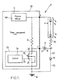
- FIG. 1 there is shown therein a schematic view of a circuit 2 for retro-lighting a display.
- the circuit 2 comprises a group 4 of white light-emitting diodes (LEDs) connected in series between a first node A and a second node B.
- LEDs white light-emitting diodes
- the circuit 2 also comprises a circuit for driving the group of LEDs.
- This driving circuit comprises a power supply 6 providing a positive voltage supplied to the first node A and a charge pump converter providing a negative voltage supplied to the second node B, obtained from the DC/DC conversion of the positive voltage.
- the positive voltage provided by the power supply 6 is, for example, issued from a DC/DC converter obtaining the positive voltage from a power supply voltage Vdd of the circuit 2.
- the output voltage of the DC/DC converter is function of the number of LEDs to be driven.
- a typical average value of the current supplied by the power supply 6 is around 50mA, but there may be some transient up to 150mA.
- the power supply 6 may have a slow voltage variation to operate a dimming on the white LEDs.
- the charge pump converter comprises a charge pump capacitor 8 having a first terminal 10 coupled to the first node A through a first resistor 12 and a second terminal 14 coupled to the second node B.
- the second terminal 14 of capacitor 8 is coupled to a ground terminal 16 through a free-wheel diode 18.
- Diode 18 has an anode 20 and a cathode 22, said anode 20 being coupled to the second node B and said cathode 22 being coupled to the ground terminal 16.
- the charge pump converter also comprises a switching element 24 connected between the first terminal 10 of the charge pump capacitor 8 (node C) and the ground terminal 16 and controlled to regulate the voltage across the charge pump capacitor 8 depending on the desired value for the negative voltage.
- the charge pump capacitor 8 may be chosen as a 10 ⁇ F ceramic capacitor. However this capacitance value can be decreased depending on a predefined switching frequency of the display. For instance, a value of 1 ⁇ F may be used.
- the resistor 12 enables to limit the current in the circuit, and thus the voltage across the capacitor 8. For example, resistor 12 insures a voltage V c across the switching element 24 of 15V when the switching element 24 is open and a voltage V c of 0V when the switching element 24 is closed. The precision of this resistor 12 is not mandatory.
- the free wheel diode 18 insures that the charge pump capacitor 8 is running between around 0V and the negative voltage, for example -15 V.
- the switching element 24 comprises a MOS transistor 26 having a first main terminal 28 coupled to the ground terminal 16, a second main terminal 30 coupled to the first terminal 10 of the charge pump capacitor 8, and a gate terminal 32.
- the MOS transistor 26 is, for example, a NMOS transistor, of which the first main terminal 28 is the source terminal and the second main terminal 30 is the drain terminal.
- the switching element 24 also comprises a control circuit 34 having a control output coupled to the gate terminal 32 of the MOS transistor 26, and configured for controlling the current through the MOS transistor 26.
- the control circuit 34 provides a control voltage for the switch 24 at the predefined switching frequency which is generally chosen higher than 50Hz so as to avoid visual problems at the display.
- control circuit 34 is able to decrease the amplitude of the output control signal in order to put the MOS transistor 26 in a region of higher resistance. In this case, the current through the MOS transistor 26 is decreased and the charge pump capacitor 8 is charged at a lower voltage i.e. the voltage V B is closer to 0V. This feature of the control circuit allows making a dimming on the white LEDs.
- the circuit 2 also comprises a second resistor 36 connected in series between the group 4 of series-coupled light-emitting diodes and the second terminal 14 of the charge pump capacitor 8.
- This second resistor 36 permits to limit the current through the white LEDs.
- the power supply 6, the switching element 24 and the first resistor 12 may be integrated in a power management unit 38.
- the circuit 2 of the invention operates as follows, with reference to Figures 2 and 3 .
- the voltages at nodes A, B, C are V A ⁇ 15 V, V B ⁇ 0V, and V c ⁇ 15V, respectively.
- the voltage supplied to the group 4 of LEDs is V AB ⁇ 15V that is to say under the sum of the threshold voltages of LEDs, and therefore the LEDs do not emit light.
- Capacitor 8 is charging under a voltage of ⁇ 15 V.
- the voltages at nodes A, B, C are V A ⁇ 15 V, V B ⁇ -15V, and V c ⁇ 0V, respectively.
- the voltage supplied to the group 4 of LEDs is V AB ⁇ 30V that is to say above the sum of the threshold voltages of LEDs and the LEDs emit light.
- the number of LEDs in series may thus be as high as 10.
- the principle of the invention is not limited to this example.
- FIG. 4 shows the elements of a device incorporating a display as presented above.
- a device can be a mobile telephone or any other telephone, or any other device for communication.
- the device 100 comprises a control unit 101 such as a processor (CPU), and a communication unit 102 for sending and receiving information from the outside, in particular by modulating a radio frequency carrier. It also comprises a memory 103 which can store information in digital form, for example a piece of video.
- the processor 101 communicates with the unit 102 and the memory 103 via a communication bus 104. Each of these elements is powered by the supply voltage Vdd delivered by a battery 106 through a control switch 107.
- this switch 107 is closed.
- the processor 101 generates a signal Vin to be displayed, either from data received via the unit 102, or from data read from the memory 103.
- the device 100 comprises a display 105 comprising a circuit 109 for retro-lighting said display whose embodiments have been described above. This display is also powered by the voltage Vdd supplied to it through the switch 107 once power is turned on.
Priority Applications (4)
| Application Number | Priority Date | Filing Date | Title |
|---|---|---|---|
| EP10305821A EP2410819A1 (de) | 2010-07-23 | 2010-07-23 | Schaltung zur Rückbeleuchtung einer Anzeige |
| US13/808,913 US8947011B2 (en) | 2010-07-23 | 2011-07-22 | Circuit for retro-lighting a display |
| EP11734160.2A EP2596679B1 (de) | 2010-07-23 | 2011-07-22 | Schaltung zur hintergrundbeleuchtung einer anzeige |
| PCT/EP2011/062691 WO2012010707A1 (en) | 2010-07-23 | 2011-07-22 | Circuit for retro-lighting a display |
Applications Claiming Priority (1)
| Application Number | Priority Date | Filing Date | Title |
|---|---|---|---|
| EP10305821A EP2410819A1 (de) | 2010-07-23 | 2010-07-23 | Schaltung zur Rückbeleuchtung einer Anzeige |
Publications (1)
| Publication Number | Publication Date |
|---|---|
| EP2410819A1 true EP2410819A1 (de) | 2012-01-25 |
Family
ID=43098927
Family Applications (2)
| Application Number | Title | Priority Date | Filing Date |
|---|---|---|---|
| EP10305821A Withdrawn EP2410819A1 (de) | 2010-07-23 | 2010-07-23 | Schaltung zur Rückbeleuchtung einer Anzeige |
| EP11734160.2A Active EP2596679B1 (de) | 2010-07-23 | 2011-07-22 | Schaltung zur hintergrundbeleuchtung einer anzeige |
Family Applications After (1)
| Application Number | Title | Priority Date | Filing Date |
|---|---|---|---|
| EP11734160.2A Active EP2596679B1 (de) | 2010-07-23 | 2011-07-22 | Schaltung zur hintergrundbeleuchtung einer anzeige |
Country Status (3)
| Country | Link |
|---|---|
| US (1) | US8947011B2 (de) |
| EP (2) | EP2410819A1 (de) |
| WO (1) | WO2012010707A1 (de) |
Families Citing this family (1)
| Publication number | Priority date | Publication date | Assignee | Title |
|---|---|---|---|---|
| US10939525B2 (en) | 2019-04-18 | 2021-03-02 | Goodrich Lighting Systems, Inc. | Driving light emitting diodes and display apparatus |
Citations (7)
| Publication number | Priority date | Publication date | Assignee | Title |
|---|---|---|---|---|
| US4809152A (en) * | 1985-10-01 | 1989-02-28 | Maxim Integrated Products | Integrated dual charge pump power supply and RS-232-transmitter/receiver |
| US6348818B1 (en) * | 2000-08-14 | 2002-02-19 | Ledi-Lite Ltd. | Voltage-adder LED driver |
| US20070001625A1 (en) * | 2005-06-30 | 2007-01-04 | Samsung Electro-Mechanics Co., Ltd. | Light emitting diode driving circuit for backlight having constant current control function |
| US20070146050A1 (en) * | 2005-12-27 | 2007-06-28 | Tien-Tzu Chen | Charge pump drive circuit for a light emitting diode |
| US20080094042A1 (en) * | 2006-10-21 | 2008-04-24 | Advanced Analogic Technologies, Inc. | Charging Scheme |
| US20080129225A1 (en) * | 2004-12-03 | 2008-06-05 | Isao Yamamoto | Power Supply Device, Light Emitting Device Using Such Power Supply Device, And Electronic Device |
| EP2043243A1 (de) * | 2007-09-27 | 2009-04-01 | ABB Schweiz AG | Umrichterschaltung sowie Verfahren zum Betrieb einer solchen Umrichterschaltung |
Family Cites Families (2)
| Publication number | Priority date | Publication date | Assignee | Title |
|---|---|---|---|---|
| TWI434611B (zh) * | 2010-02-25 | 2014-04-11 | Richtek Technology Corp | 具有電壓調整功能之led陣列控制電路及其驅動電路與方法 |
| KR101208576B1 (ko) * | 2010-08-25 | 2012-12-06 | 주식회사 동부하이텍 | 발광소자 구동 장치 |
-
2010
- 2010-07-23 EP EP10305821A patent/EP2410819A1/de not_active Withdrawn
-
2011
- 2011-07-22 EP EP11734160.2A patent/EP2596679B1/de active Active
- 2011-07-22 WO PCT/EP2011/062691 patent/WO2012010707A1/en active Application Filing
- 2011-07-22 US US13/808,913 patent/US8947011B2/en active Active
Patent Citations (7)
| Publication number | Priority date | Publication date | Assignee | Title |
|---|---|---|---|---|
| US4809152A (en) * | 1985-10-01 | 1989-02-28 | Maxim Integrated Products | Integrated dual charge pump power supply and RS-232-transmitter/receiver |
| US6348818B1 (en) * | 2000-08-14 | 2002-02-19 | Ledi-Lite Ltd. | Voltage-adder LED driver |
| US20080129225A1 (en) * | 2004-12-03 | 2008-06-05 | Isao Yamamoto | Power Supply Device, Light Emitting Device Using Such Power Supply Device, And Electronic Device |
| US20070001625A1 (en) * | 2005-06-30 | 2007-01-04 | Samsung Electro-Mechanics Co., Ltd. | Light emitting diode driving circuit for backlight having constant current control function |
| US20070146050A1 (en) * | 2005-12-27 | 2007-06-28 | Tien-Tzu Chen | Charge pump drive circuit for a light emitting diode |
| US20080094042A1 (en) * | 2006-10-21 | 2008-04-24 | Advanced Analogic Technologies, Inc. | Charging Scheme |
| EP2043243A1 (de) * | 2007-09-27 | 2009-04-01 | ABB Schweiz AG | Umrichterschaltung sowie Verfahren zum Betrieb einer solchen Umrichterschaltung |
Also Published As
| Publication number | Publication date |
|---|---|
| US20130234592A1 (en) | 2013-09-12 |
| EP2596679A1 (de) | 2013-05-29 |
| EP2596679B1 (de) | 2014-05-14 |
| US8947011B2 (en) | 2015-02-03 |
| WO2012010707A1 (en) | 2012-01-26 |
Similar Documents
| Publication | Publication Date | Title |
|---|---|---|
| TWI398083B (zh) | 直流/直流轉換器、操作直流/直流轉換器的方法、直流/直流轉換器的切換電路、以及包含直流/直流轉換器的裝置 | |
| CN100440697C (zh) | 电荷泵电路的驱动电路和电源装置及发光装置 | |
| US20080136771A1 (en) | Backlight control circuit with primary and secondary switch units | |
| US9185763B2 (en) | Light emitting diode string driving method | |
| US8111007B2 (en) | Electronic device capable of controlling LED brightness and method thereof | |
| WO2016074356A1 (zh) | 一种像素电路、显示面板及其驱动方法 | |
| KR20050041945A (ko) | 발광 소자 구동 장치, 발광 소자 구동 장치를 포함하는표시 모듈 및 표시 모듈을 구비하는 전자 기기 | |
| US10504434B2 (en) | DC-DC converter and display device having the same | |
| CN202549254U (zh) | 大功率led背光源驱动电路 | |
| US9414461B2 (en) | DC-DC converter and organic light emitting display device including the same | |
| JP2006254641A (ja) | チャージポンプ式ledドライバおよびチャージポンプの昇圧率切換え方法 | |
| US7531971B2 (en) | Backlight units and display devices | |
| CN102622986A (zh) | 一种 led 背光驱动电路、背光模组和液晶显示装置 | |
| CN103745691B (zh) | 背光驱动电路以及液晶显示装置 | |
| CN101562933B (zh) | 一种背光模块的驱动电路 | |
| EP2596679B1 (de) | Schaltung zur hintergrundbeleuchtung einer anzeige | |
| US20110279041A1 (en) | Illumination apparatus and brightness adjusting method thereof | |
| CN100539369C (zh) | 驱动电路 | |
| CN101950541B (zh) | 背光模块及液晶显示器 | |
| US8111214B2 (en) | Charge recovery for enhanced transistor drive | |
| CN103927983B (zh) | 像素电路、显示基板和显示装置 | |
| TW201248589A (en) | Pixel structure and display system utilizing the same | |
| US8791654B2 (en) | Pulse width modulation circuit and illumination apparatus | |
| JP2009541783A (ja) | エレクトロルミネッセンス表示装置駆動用電子回路 | |
| Park et al. | 135-channel electronic-paper driver ic for electronic shelf label |
Legal Events
| Date | Code | Title | Description |
|---|---|---|---|
| AK | Designated contracting states |
Kind code of ref document: A1 Designated state(s): AL AT BE BG CH CY CZ DE DK EE ES FI FR GB GR HR HU IE IS IT LI LT LU LV MC MK MT NL NO PL PT RO SE SI SK SM TR |
|
| AX | Request for extension of the european patent |
Extension state: BA ME RS |
|
| PUAI | Public reference made under article 153(3) epc to a published international application that has entered the european phase |
Free format text: ORIGINAL CODE: 0009012 |
|
| STAA | Information on the status of an ep patent application or granted ep patent |
Free format text: STATUS: THE APPLICATION IS DEEMED TO BE WITHDRAWN |
|
| 18D | Application deemed to be withdrawn |
Effective date: 20120726 |