EP2407883A1 - Copyback optimization for memory system - Google Patents
Copyback optimization for memory system Download PDFInfo
- Publication number
- EP2407883A1 EP2407883A1 EP11183929A EP11183929A EP2407883A1 EP 2407883 A1 EP2407883 A1 EP 2407883A1 EP 11183929 A EP11183929 A EP 11183929A EP 11183929 A EP11183929 A EP 11183929A EP 2407883 A1 EP2407883 A1 EP 2407883A1
- Authority
- EP
- European Patent Office
- Prior art keywords
- data page
- data
- changed
- volatile memory
- memory
- Prior art date
- Legal status (The legal status is an assumption and is not a legal conclusion. Google has not performed a legal analysis and makes no representation as to the accuracy of the status listed.)
- Granted
Links
Images


Classifications
-
- G—PHYSICS
- G06—COMPUTING OR CALCULATING; COUNTING
- G06F—ELECTRIC DIGITAL DATA PROCESSING
- G06F11/00—Error detection; Error correction; Monitoring
- G06F11/07—Responding to the occurrence of a fault, e.g. fault tolerance
- G06F11/08—Error detection or correction by redundancy in data representation, e.g. by using checking codes
- G06F11/10—Adding special bits or symbols to the coded information, e.g. parity check, casting out 9's or 11's
- G06F11/1008—Adding special bits or symbols to the coded information, e.g. parity check, casting out 9's or 11's in individual solid state devices
- G06F11/1068—Adding special bits or symbols to the coded information, e.g. parity check, casting out 9's or 11's in individual solid state devices in sector programmable memories, e.g. flash disk
-
- G—PHYSICS
- G11—INFORMATION STORAGE
- G11C—STATIC STORES
- G11C16/00—Erasable programmable read-only memories
- G11C16/02—Erasable programmable read-only memories electrically programmable
- G11C16/06—Auxiliary circuits, e.g. for writing into memory
-
- G—PHYSICS
- G06—COMPUTING OR CALCULATING; COUNTING
- G06F—ELECTRIC DIGITAL DATA PROCESSING
- G06F11/00—Error detection; Error correction; Monitoring
- G06F11/07—Responding to the occurrence of a fault, e.g. fault tolerance
- G06F11/08—Error detection or correction by redundancy in data representation, e.g. by using checking codes
- G06F11/10—Adding special bits or symbols to the coded information, e.g. parity check, casting out 9's or 11's
Definitions
- This subject matter is generally related to memory systems.
- Flash memory is a type of electrically erasable programmable read-only memory (EEPROM). Because flash memories are non-volatile and relatively dense, they are used to store files and other persistent objects in handheld computers, mobile phones, digital cameras, portable music players, and many other devices in which other storage solutions (e.g., magnetic disks) are inappropriate.
- EEPROM electrically erasable programmable read-only memory
- data page change indicators are used to manage transfers of data pages between a register in non-volatile memory and a controller that is external to the non-volatile memory.
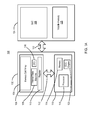
- FIG. 1A is a block diagram of an example memory system for implementing an optimized copyback process.
- FIG. IB is a block diagram of another example memory system for implementing an optimized copyback process.
- FIG. 2 is a flow diagram of an example optimized copyback process 200 for computing and storing data change indicators used by the memory systems of FIGS. 1A and IB.
- FIGS. 3A-3C are flow diagrams of an example optimized copyback process implemented by the memory systems of FIGS. 1A and IB.
- FIG. 4 is a flow diagram of an example optimized read operation implemented by the memory systems of FIGS. 1A and IB.
- FIG. 5 illustrates example data structures used by the copyback process of FIGS. 3A-3C .
- FIG. 1A is a block diagram of an example memory system 100 for implementing an optimized copyback process.
- the system 100 can include a memory subsystem 102 coupled to a host device 124 through an external bus 122 (e.g., Open NAND Flash Interface (ONFI), ATA).
- the host device 124 can be any electronic device including but not limited to smart phones, media players, text messaging devices, portable computers, solid state drives, digital cameras, etc.
- the memory subsystem 102 can be any non-volatile memory subsystem (e.g., managed NAND).
- the host device 124 can include a system-on-chip (SoC) 126 and volatile memory 128.
- SoC system-on-chip
- the SoC 126 can include hardware and software for interacting with the memory subsystem 102, such as transmitting read and write requests made by applications running on the host device 124.
- the memory subsystem 102 can include non-volatile memory 104 (also referred to as "raw memory") and an external controller 116.
- the memory 104 can include a memory cell array 106, an internal state machine 108, a memory register 110 and data change indicator (DO) 130.
- the controller 116 can include a processor 118, volatile memory 114 and error correction code (ECC) engine 120.
- ECC error correction code
- Other configurations for the memory subsystem 102 are possible.
- a cache register can be included in the data path between the memory cell array 106 and the memory register 110 to allow the internal state machine to read the next data page from the memory cell array 106 while transferring the current page to the controller 116 over internal bus 112.
- FIG. IB is a block diagram of another example memory system 130 for implementing an optimized copyback process.
- the system 130 shows only the memory subsystem 102, the operation of which was described in reference to FIG. 1A .
- Copyback can be a memory subsystem command to move data from one page to another page. Copyback can be used in wear leveling and other nonvolatile memory management operations.
- a data page is read from the memory cell array 106 and stored in the memory register 110 by the internal state machine.
- the external controller 116 reads or clocks the data page out of the memory register 110 so that the processor 118 can perform a desired operation on the data page (e.g., an ECC operation).
- the processed data page can be written back to the memory register 110 by the controller 116.
- the internal state machine 108 can write the contents of the memory register 110 into a new data page in the memory cell array 106.
- FIG. 2 is a flow diagram of an example optimized copyback process 200 for computing and storing data change indicators used by the memory systems of FIGS. 1A and IB.
- the process 200 can begin when new data page is transferred into a memory register of a memory subsystem (202).
- a DCI can be computed for the data page and stored in the memory subsystem (204).
- Some examples of data change indicators can include error detection codes (EDCs), including but not limited to: checksum, Hamming code, parity bit, cyclic redundancy check (CRC), polarity symbol reversal, Turbo code, etc.
- EDCs error detection codes
- CRC cyclic redundancy check
- An EDC can also be part of an ECC, such as Reed-Solomon code, Reed-Muller code, Binary Golay code, and low-density parity-check codes.
- FIGS. 3A-3C are flow diagrams of an example optimized copyback process 300 implemented by the memory systems of FIGS. 1A and IB.
- the process 300 can begin by reading a data page from non-volatile memory (e.g., memory cell array 106) and storing the data page in a memory register (302) (e.g., register 110).
- a DCI e.g., DCI130
- the DCI can be verified for the data page in the memory register (304).
- the DCI can be previously computed and stored in the memory subsystem when the data page is first written to non-volatile memory (e.g., using process 200).
- the DCI can be computed "on the fly" as part of the read operation or as a separate operation.
- the memory subsystem can report to an external controller (e.g., external controller 116) that the read operation has completed (306).
- the data page can be transferred to the external controller (310), an ECC can be computed for the data page (312) and the ECC information for the data page can be corrected in the external controller (314).
- the data page and associated ECC can be transferred back to the memory register (316).
- a new DCI can be computed for the data page in the memory register (318).
- an ECC can be computed for new metadata associated with the data page (320).
- the new metadata and associated ECC can be transferred to the memory register (322).
- a new DCI can be computed for the metadata in the memory register (324).
- the memory register contents can be written to a new data page in non-volatile memory (326).
- FIG. 4 is a flow diagram of an example optimized read operation implemented by the memory systems of FIGS. 1A and IB.
- the process 400 can begin by reading a data page from non-volatile memory and storing the data page in a memory register (402).
- a pre-computed DCI associated with the data page can be clocked into the memory register from a storage location in the memory subsystem and verified (404).
- the DCI can also be computed "on the fly.”
- the status of the DCI can be read to determine if the data page has changed (406).
- an ECC for the new metadata associated with the data page can be computed and transferred, together with the new metadata to the memory register (412).
- a new DCI can be computed for the metadata in the memory register and the register contents can be written to a new data page in non-volatile memory (414).
- the memory register contents can be transferred to an external controller and an ECC can be computed by the external controller (410).
- An ECC for the new metadata associated with the data page can be computed and transferred by the external controller, together with the new metadata to the memory register (412).
- a new DCI can be computed for the metadata in the memory register and the register contents can be written to a new data page in non-volatile memory (414).
- FIG. 5 illustrates example data structures used by the copyback process of FIGS. 3A-3C .
- a data page 500 in non-volatile memory includes metadata 502, metadata ECC 504, data 506 and data ECC 508. If the data has not changed than only the metadata 502 and the metadata ECC 504 are transferred from the register to the external controller 510 for processing. The processed metadata 502 and metadata ECC 504 are transferred back to the memory subsystem and stored in the memory register. The data page can the be written to a new data page in non-volatile memory (e.g., a memory cell array).
- non-volatile memory e.g., a memory cell array
Landscapes
- Engineering & Computer Science (AREA)
- Theoretical Computer Science (AREA)
- Quality & Reliability (AREA)
- Physics & Mathematics (AREA)
- General Engineering & Computer Science (AREA)
- General Physics & Mathematics (AREA)
- Techniques For Improving Reliability Of Storages (AREA)
- Exchange Systems With Centralized Control (AREA)
Abstract
Description
- This subject matter is generally related to memory systems.
- Flash memory is a type of electrically erasable programmable read-only memory (EEPROM). Because flash memories are non-volatile and relatively dense, they are used to store files and other persistent objects in handheld computers, mobile phones, digital cameras, portable music players, and many other devices in which other storage solutions (e.g., magnetic disks) are inappropriate. When data stored in flash memory is processed, a data page is read out of flash memory and stored in a register. The register contents is transferred to a controller that is external to the non-volatile memory for processing. The processed data page is placed back in the register so that the processed data page can be written back to flash memory.
- In a copyback or read operation for a non-volatile memory subsystem, data page change indicators are used to manage transfers of data pages between a register in non-volatile memory and a controller that is external to the non-volatile memory.
-
FIG. 1A is a block diagram of an example memory system for implementing an optimized copyback process. - FIG. IB is a block diagram of another example memory system for implementing an optimized copyback process.
-
FIG. 2 is a flow diagram of an example optimizedcopyback process 200 for computing and storing data change indicators used by the memory systems ofFIGS. 1A and IB. -
FIGS. 3A-3C are flow diagrams of an example optimized copyback process implemented by the memory systems ofFIGS. 1A and IB. -
FIG. 4 is a flow diagram of an example optimized read operation implemented by the memory systems ofFIGS. 1A and IB. -
FIG. 5 illustrates example data structures used by the copyback process ofFIGS. 3A-3C . -
FIG. 1A is a block diagram of anexample memory system 100 for implementing an optimized copyback process. In some implementations, thesystem 100 can include amemory subsystem 102 coupled to ahost device 124 through an external bus 122 (e.g., Open NAND Flash Interface (ONFI), ATA). Thehost device 124 can be any electronic device including but not limited to smart phones, media players, text messaging devices, portable computers, solid state drives, digital cameras, etc. Thememory subsystem 102 can be any non-volatile memory subsystem (e.g., managed NAND). - The
host device 124 can include a system-on-chip (SoC) 126 andvolatile memory 128. The SoC 126 can include hardware and software for interacting with thememory subsystem 102, such as transmitting read and write requests made by applications running on thehost device 124. - The
memory subsystem 102 can include non-volatile memory 104 (also referred to as "raw memory") and anexternal controller 116. Thememory 104 can include amemory cell array 106, aninternal state machine 108, amemory register 110 and data change indicator (DO) 130. Thecontroller 116 can include aprocessor 118,volatile memory 114 and error correction code (ECC)engine 120. Other configurations for thememory subsystem 102 are possible. For example, a cache register can be included in the data path between thememory cell array 106 and thememory register 110 to allow the internal state machine to read the next data page from thememory cell array 106 while transferring the current page to thecontroller 116 overinternal bus 112. - FIG. IB is a block diagram of another
example memory system 130 for implementing an optimized copyback process. Thesystem 130 shows only thememory subsystem 102, the operation of which was described in reference toFIG. 1A . - Copyback can be a memory subsystem command to move data from one page to another page. Copyback can be used in wear leveling and other nonvolatile memory management operations. In a typical copyback operation, a data page is read from the
memory cell array 106 and stored in thememory register 110 by the internal state machine. Theexternal controller 116 reads or clocks the data page out of thememory register 110 so that theprocessor 118 can perform a desired operation on the data page (e.g., an ECC operation). The processed data page can be written back to thememory register 110 by thecontroller 116. Theinternal state machine 108 can write the contents of thememory register 110 into a new data page in thememory cell array 106. By avoiding the transfer of the entire contents ofregister 110 to theexternal controller 116, processing times and power consumption can be reduced. -
FIG. 2 is a flow diagram of an example optimizedcopyback process 200 for computing and storing data change indicators used by the memory systems ofFIGS. 1A and IB. In some implementations, theprocess 200 can begin when new data page is transferred into a memory register of a memory subsystem (202). A DCI can be computed for the data page and stored in the memory subsystem (204). Some examples of data change indicators can include error detection codes (EDCs), including but not limited to: checksum, Hamming code, parity bit, cyclic redundancy check (CRC), polarity symbol reversal, Turbo code, etc. An EDC can also be part of an ECC, such as Reed-Solomon code, Reed-Muller code, Binary Golay code, and low-density parity-check codes. After the DCIs are computed and stored, the register contents can be written to non-volatile memory (206). DCIs can be used for the optimized copyback process described in reference toFIGS. 3A-3C . -
FIGS. 3A-3C are flow diagrams of an example optimizedcopyback process 300 implemented by the memory systems ofFIGS. 1A and IB. In some implementations, theprocess 300 can begin by reading a data page from non-volatile memory (e.g., memory cell array 106) and storing the data page in a memory register (302) (e.g., register 110). A DCI (e.g., DCI130) can be verified for the data page in the memory register (304). In some implementations, the DCI can be previously computed and stored in the memory subsystem when the data page is first written to non-volatile memory (e.g., using process 200). In other implementations, the DCI can be computed "on the fly" as part of the read operation or as a separate operation. The memory subsystem can report to an external controller (e.g., external controller 116) that the read operation has completed (306). - If the DCI for the data page in the register indicates that the data page has changed (308), the data page can be transferred to the external controller (310), an ECC can be computed for the data page (312) and the ECC information for the data page can be corrected in the external controller (314). The data page and associated ECC can be transferred back to the memory register (316). A new DCI can be computed for the data page in the memory register (318).
- If the DCI for the data page in the register indicates that the data page has not changed (308), an ECC can be computed for new metadata associated with the data page (320). The new metadata and associated ECC can be transferred to the memory register (322). A new DCI can be computed for the metadata in the memory register (324). The memory register contents can be written to a new data page in non-volatile memory (326).
-
FIG. 4 is a flow diagram of an example optimized read operation implemented by the memory systems ofFIGS. 1A and IB. In some implementations, theprocess 400 can begin by reading a data page from non-volatile memory and storing the data page in a memory register (402). A pre-computed DCI associated with the data page can be clocked into the memory register from a storage location in the memory subsystem and verified (404). The DCI can also be computed "on the fly." The status of the DCI can be read to determine if the data page has changed (406). - If the data page has changed (408), an ECC for the new metadata associated with the data page can be computed and transferred, together with the new metadata to the memory register (412). A new DCI can be computed for the metadata in the memory register and the register contents can be written to a new data page in non-volatile memory (414).
- If the data page has not changed (408), the memory register contents can be transferred to an external controller and an ECC can be computed by the external controller (410). An ECC for the new metadata associated with the data page can be computed and transferred by the external controller, together with the new metadata to the memory register (412). A new DCI can be computed for the metadata in the memory register and the register contents can be written to a new data page in non-volatile memory (414).
-
FIG. 5 illustrates example data structures used by the copyback process ofFIGS. 3A-3C . In the example shown, adata page 500 in non-volatile memory includesmetadata 502,metadata ECC 504,data 506 anddata ECC 508. If the data has not changed than only themetadata 502 and themetadata ECC 504 are transferred from the register to theexternal controller 510 for processing. The processedmetadata 502 andmetadata ECC 504 are transferred back to the memory subsystem and stored in the memory register. The data page can the be written to a new data page in non-volatile memory (e.g., a memory cell array). - A number of implementations have been described. Nevertheless, it will be understood that various modifications may be made. For example, elements of one or more implementations may be combined, deleted, modified, or supplemented to form further implementations. As yet another example, the logic flows depicted in the figures do not require the particular order shown, or sequential order, to achieve desirable results. In addition, other steps may be provided, or steps may be eliminated, from the described flows, and other components may be added to, or removed from, the described systems. Accordingly, other implementations are within the scope of the following claims.
Claims (18)
- A method comprising:obtaining a data page from non-volatile memory of a memory subsystem;determining if the data page has changed; andif the data page has changed,sending the data page to a controller for processing;if the data page is unchanged,sending metadata associated with the data page to the controller for processing.
- The method of claim 1, where determining if the data page has changed further comprises:reading a data change indicator for the data page.
- The method of claim 2, where the data change indicator is associated with an error detection code.
- The method of claim 1, where determining if the data page has changed further comprises:computing a data change indicator for the data page; anddetermining if the data page has changed based on the data change indicator.
- The method of claim 4, where computing the data change indicator is performed prior to or concurrently with obtaining the data page from the non-volatile memory.
- The method of claim 1, where if the data page has changed, the method further comprising:determining, by the controller, an error correction code associated with the data page that has changed.
- The method of claim 6, where obtaining the data page includes obtaining the data page from a register, the method further comprising:sending the data page that has changed and the error correction code to the register.
- The method of claim 1, where if the data page is unchanged, the method further comprising:determining, by the controller, an error correction code for the metadata associated with the unchanged data page; andsending the associated metadata and the error correction code to the non-volatile memory.
- The method of claim 8, where sending the associated metadata and the error correction code to the non-volatile memory includes:writing the associated metadata to a register associated with the non-volatile memory; andwriting the unchanged data page to a new data page in the non-volatile memory.
- A system comprising:an interface adapted for coupling to a controller;non-volatile memory;a processor coupled to the non-volatile memory and the interface, the processor operable to:obtain a data page from the non-volatile memory;determine if the data page has changed; andif the data page has changed, send the data page through the interface to the controller for processing;if the data page has not changed,send metadata associated with the data page through the interface to the controller for processing.
- The system of claim 10, where the processor is further operable to read a data change indicator for the data page to determine if the data page has changed.
- The system of claim 11, where the data change indicator is associated with an error detection code.
- The system of claim 10, where the processor is further operable to compute a data change indicator for the data page, and determine if the data page has changed based on the data change indicator.
- The system of claim 13, where the processor is further operable to compute the data change indicator prior to or concurrently with obtaining the data page from the non-volatile memory.
- The system of claim 10, where if the data page has changed, the controller is further operable to determine an error correction code associated with the data page that has changed.
- The system of claim 15, where:the processor is further operable to obtain the data page from a register; andthe controller is further operable to send the data page that has changed and the error correction code to the register.
- The system of claim 10, where if the data page is unchanged, the controller is further operable to:determine an error correction code for the metadata associated with the unchanged data page; andsend the associated metadata and the error correction code to the non-volatile memory.
- The system of claim 17, where the controller is further operable to:write the associated metadata to a register associated with the non-volatile memory; andwrite the unchanged data page to a new data page in the non-volatile memory.
Applications Claiming Priority (3)
| Application Number | Priority Date | Filing Date | Title |
|---|---|---|---|
| US4933008P | 2008-04-30 | 2008-04-30 | |
| US12/193,638 US8185706B2 (en) | 2008-04-30 | 2008-08-18 | Copyback optimization for memory system |
| EP09739378A EP2297642B1 (en) | 2008-04-30 | 2009-04-01 | Copyback optimization for memory system |
Related Parent Applications (1)
| Application Number | Title | Priority Date | Filing Date |
|---|---|---|---|
| EP09739378.9 Division | 2009-04-01 |
Publications (2)
| Publication Number | Publication Date |
|---|---|
| EP2407883A1 true EP2407883A1 (en) | 2012-01-18 |
| EP2407883B1 EP2407883B1 (en) | 2013-08-21 |
Family
ID=40801795
Family Applications (2)
| Application Number | Title | Priority Date | Filing Date |
|---|---|---|---|
| EP09739378A Not-in-force EP2297642B1 (en) | 2008-04-30 | 2009-04-01 | Copyback optimization for memory system |
| EP11183929.6A Not-in-force EP2407883B1 (en) | 2008-04-30 | 2009-04-01 | Copyback optimization for memory system |
Family Applications Before (1)
| Application Number | Title | Priority Date | Filing Date |
|---|---|---|---|
| EP09739378A Not-in-force EP2297642B1 (en) | 2008-04-30 | 2009-04-01 | Copyback optimization for memory system |
Country Status (8)
| Country | Link |
|---|---|
| US (2) | US8185706B2 (en) |
| EP (2) | EP2297642B1 (en) |
| JP (1) | JP5192587B2 (en) |
| KR (2) | KR101225924B1 (en) |
| CN (1) | CN102077176B (en) |
| AT (1) | ATE535866T1 (en) |
| ES (1) | ES2378371T3 (en) |
| WO (1) | WO2009134576A1 (en) |
Families Citing this family (82)
| Publication number | Priority date | Publication date | Assignee | Title |
|---|---|---|---|---|
| US7978516B2 (en) | 2007-12-27 | 2011-07-12 | Pliant Technology, Inc. | Flash memory controller having reduced pinout |
| US8443263B2 (en) * | 2009-12-30 | 2013-05-14 | Sandisk Technologies Inc. | Method and controller for performing a copy-back operation |
| US8365041B2 (en) | 2010-03-17 | 2013-01-29 | Sandisk Enterprise Ip Llc | MLC self-raid flash data protection scheme |
| KR101844346B1 (en) * | 2010-11-05 | 2018-04-02 | 삼성전자주식회사 | Memory system and method of operating a memory system |
| US8910020B2 (en) | 2011-06-19 | 2014-12-09 | Sandisk Enterprise Ip Llc | Intelligent bit recovery for flash memory |
| US8909982B2 (en) | 2011-06-19 | 2014-12-09 | Sandisk Enterprise Ip Llc | System and method for detecting copyback programming problems |
| US9058289B2 (en) | 2011-11-07 | 2015-06-16 | Sandisk Enterprise Ip Llc | Soft information generation for memory systems |
| US8954822B2 (en) | 2011-11-18 | 2015-02-10 | Sandisk Enterprise Ip Llc | Data encoder and decoder using memory-specific parity-check matrix |
| US9048876B2 (en) | 2011-11-18 | 2015-06-02 | Sandisk Enterprise Ip Llc | Systems, methods and devices for multi-tiered error correction |
| US8924815B2 (en) | 2011-11-18 | 2014-12-30 | Sandisk Enterprise Ip Llc | Systems, methods and devices for decoding codewords having multiple parity segments |
| US9699263B1 (en) | 2012-08-17 | 2017-07-04 | Sandisk Technologies Llc. | Automatic read and write acceleration of data accessed by virtual machines |
| US9501398B2 (en) | 2012-12-26 | 2016-11-22 | Sandisk Technologies Llc | Persistent storage device with NVRAM for staging writes |
| US9612948B2 (en) | 2012-12-27 | 2017-04-04 | Sandisk Technologies Llc | Reads and writes between a contiguous data block and noncontiguous sets of logical address blocks in a persistent storage device |
| US9239751B1 (en) | 2012-12-27 | 2016-01-19 | Sandisk Enterprise Ip Llc | Compressing data from multiple reads for error control management in memory systems |
| US9454420B1 (en) | 2012-12-31 | 2016-09-27 | Sandisk Technologies Llc | Method and system of reading threshold voltage equalization |
| US9003264B1 (en) | 2012-12-31 | 2015-04-07 | Sandisk Enterprise Ip Llc | Systems, methods, and devices for multi-dimensional flash RAID data protection |
| US9329928B2 (en) | 2013-02-20 | 2016-05-03 | Sandisk Enterprise IP LLC. | Bandwidth optimization in a non-volatile memory system |
| US9214965B2 (en) | 2013-02-20 | 2015-12-15 | Sandisk Enterprise Ip Llc | Method and system for improving data integrity in non-volatile storage |
| US9870830B1 (en) | 2013-03-14 | 2018-01-16 | Sandisk Technologies Llc | Optimal multilevel sensing for reading data from a storage medium |
| US9136877B1 (en) | 2013-03-15 | 2015-09-15 | Sandisk Enterprise Ip Llc | Syndrome layered decoding for LDPC codes |
| US9244763B1 (en) | 2013-03-15 | 2016-01-26 | Sandisk Enterprise Ip Llc | System and method for updating a reading threshold voltage based on symbol transition information |
| US9092350B1 (en) | 2013-03-15 | 2015-07-28 | Sandisk Enterprise Ip Llc | Detection and handling of unbalanced errors in interleaved codewords |
| US9009576B1 (en) | 2013-03-15 | 2015-04-14 | Sandisk Enterprise Ip Llc | Adaptive LLR based on syndrome weight |
| US9367246B2 (en) | 2013-03-15 | 2016-06-14 | Sandisk Technologies Inc. | Performance optimization of data transfer for soft information generation |
| US9236886B1 (en) | 2013-03-15 | 2016-01-12 | Sandisk Enterprise Ip Llc | Universal and reconfigurable QC-LDPC encoder |
| US10049037B2 (en) | 2013-04-05 | 2018-08-14 | Sandisk Enterprise Ip Llc | Data management in a storage system |
| US9170941B2 (en) | 2013-04-05 | 2015-10-27 | Sandisk Enterprises IP LLC | Data hardening in a storage system |
| US9524235B1 (en) | 2013-07-25 | 2016-12-20 | Sandisk Technologies Llc | Local hash value generation in non-volatile data storage systems |
| US9384126B1 (en) | 2013-07-25 | 2016-07-05 | Sandisk Technologies Inc. | Methods and systems to avoid false negative results in bloom filters implemented in non-volatile data storage systems |
| US9043517B1 (en) | 2013-07-25 | 2015-05-26 | Sandisk Enterprise Ip Llc | Multipass programming in buffers implemented in non-volatile data storage systems |
| US9639463B1 (en) | 2013-08-26 | 2017-05-02 | Sandisk Technologies Llc | Heuristic aware garbage collection scheme in storage systems |
| US9361221B1 (en) | 2013-08-26 | 2016-06-07 | Sandisk Technologies Inc. | Write amplification reduction through reliable writes during garbage collection |
| US9519577B2 (en) | 2013-09-03 | 2016-12-13 | Sandisk Technologies Llc | Method and system for migrating data between flash memory devices |
| US9442670B2 (en) | 2013-09-03 | 2016-09-13 | Sandisk Technologies Llc | Method and system for rebalancing data stored in flash memory devices |
| US9158349B2 (en) | 2013-10-04 | 2015-10-13 | Sandisk Enterprise Ip Llc | System and method for heat dissipation |
| US9323637B2 (en) | 2013-10-07 | 2016-04-26 | Sandisk Enterprise Ip Llc | Power sequencing and data hardening architecture |
| US9298608B2 (en) | 2013-10-18 | 2016-03-29 | Sandisk Enterprise Ip Llc | Biasing for wear leveling in storage systems |
| US9442662B2 (en) | 2013-10-18 | 2016-09-13 | Sandisk Technologies Llc | Device and method for managing die groups |
| US9436831B2 (en) | 2013-10-30 | 2016-09-06 | Sandisk Technologies Llc | Secure erase in a memory device |
| US9263156B2 (en) | 2013-11-07 | 2016-02-16 | Sandisk Enterprise Ip Llc | System and method for adjusting trip points within a storage device |
| US9244785B2 (en) | 2013-11-13 | 2016-01-26 | Sandisk Enterprise Ip Llc | Simulated power failure and data hardening |
| US9152555B2 (en) | 2013-11-15 | 2015-10-06 | Sandisk Enterprise IP LLC. | Data management with modular erase in a data storage system |
| US9703816B2 (en) | 2013-11-19 | 2017-07-11 | Sandisk Technologies Llc | Method and system for forward reference logging in a persistent datastore |
| US9520197B2 (en) | 2013-11-22 | 2016-12-13 | Sandisk Technologies Llc | Adaptive erase of a storage device |
| US9280429B2 (en) | 2013-11-27 | 2016-03-08 | Sandisk Enterprise Ip Llc | Power fail latching based on monitoring multiple power supply voltages in a storage device |
| US9122636B2 (en) | 2013-11-27 | 2015-09-01 | Sandisk Enterprise Ip Llc | Hard power fail architecture |
| US9520162B2 (en) | 2013-11-27 | 2016-12-13 | Sandisk Technologies Llc | DIMM device controller supervisor |
| US9250676B2 (en) | 2013-11-29 | 2016-02-02 | Sandisk Enterprise Ip Llc | Power failure architecture and verification |
| US9582058B2 (en) | 2013-11-29 | 2017-02-28 | Sandisk Technologies Llc | Power inrush management of storage devices |
| US9092370B2 (en) | 2013-12-03 | 2015-07-28 | Sandisk Enterprise Ip Llc | Power failure tolerant cryptographic erase |
| US9235245B2 (en) | 2013-12-04 | 2016-01-12 | Sandisk Enterprise Ip Llc | Startup performance and power isolation |
| US9129665B2 (en) | 2013-12-17 | 2015-09-08 | Sandisk Enterprise Ip Llc | Dynamic brownout adjustment in a storage device |
| US9549457B2 (en) | 2014-02-12 | 2017-01-17 | Sandisk Technologies Llc | System and method for redirecting airflow across an electronic assembly |
| US9703636B2 (en) | 2014-03-01 | 2017-07-11 | Sandisk Technologies Llc | Firmware reversion trigger and control |
| US9485851B2 (en) | 2014-03-14 | 2016-11-01 | Sandisk Technologies Llc | Thermal tube assembly structures |
| US9519319B2 (en) | 2014-03-14 | 2016-12-13 | Sandisk Technologies Llc | Self-supporting thermal tube structure for electronic assemblies |
| US9348377B2 (en) | 2014-03-14 | 2016-05-24 | Sandisk Enterprise Ip Llc | Thermal isolation techniques |
| US9390814B2 (en) | 2014-03-19 | 2016-07-12 | Sandisk Technologies Llc | Fault detection and prediction for data storage elements |
| US9448876B2 (en) | 2014-03-19 | 2016-09-20 | Sandisk Technologies Llc | Fault detection and prediction in storage devices |
| US9454448B2 (en) | 2014-03-19 | 2016-09-27 | Sandisk Technologies Llc | Fault testing in storage devices |
| US9626399B2 (en) | 2014-03-31 | 2017-04-18 | Sandisk Technologies Llc | Conditional updates for reducing frequency of data modification operations |
| US9390021B2 (en) | 2014-03-31 | 2016-07-12 | Sandisk Technologies Llc | Efficient cache utilization in a tiered data structure |
| US9626400B2 (en) | 2014-03-31 | 2017-04-18 | Sandisk Technologies Llc | Compaction of information in tiered data structure |
| US9697267B2 (en) | 2014-04-03 | 2017-07-04 | Sandisk Technologies Llc | Methods and systems for performing efficient snapshots in tiered data structures |
| US9093160B1 (en) | 2014-05-30 | 2015-07-28 | Sandisk Technologies Inc. | Methods and systems for staggered memory operations |
| US8891303B1 (en) | 2014-05-30 | 2014-11-18 | Sandisk Technologies Inc. | Method and system for dynamic word line based configuration of a three-dimensional memory device |
| US9645749B2 (en) | 2014-05-30 | 2017-05-09 | Sandisk Technologies Llc | Method and system for recharacterizing the storage density of a memory device or a portion thereof |
| US10656840B2 (en) | 2014-05-30 | 2020-05-19 | Sandisk Technologies Llc | Real-time I/O pattern recognition to enhance performance and endurance of a storage device |
| US9703491B2 (en) | 2014-05-30 | 2017-07-11 | Sandisk Technologies Llc | Using history of unaligned writes to cache data and avoid read-modify-writes in a non-volatile storage device |
| US9070481B1 (en) | 2014-05-30 | 2015-06-30 | Sandisk Technologies Inc. | Internal current measurement for age measurements |
| US10656842B2 (en) | 2014-05-30 | 2020-05-19 | Sandisk Technologies Llc | Using history of I/O sizes and I/O sequences to trigger coalesced writes in a non-volatile storage device |
| US10162748B2 (en) | 2014-05-30 | 2018-12-25 | Sandisk Technologies Llc | Prioritizing garbage collection and block allocation based on I/O history for logical address regions |
| US10114557B2 (en) | 2014-05-30 | 2018-10-30 | Sandisk Technologies Llc | Identification of hot regions to enhance performance and endurance of a non-volatile storage device |
| US10146448B2 (en) | 2014-05-30 | 2018-12-04 | Sandisk Technologies Llc | Using history of I/O sequences to trigger cached read ahead in a non-volatile storage device |
| US10372613B2 (en) | 2014-05-30 | 2019-08-06 | Sandisk Technologies Llc | Using sub-region I/O history to cache repeatedly accessed sub-regions in a non-volatile storage device |
| US9652381B2 (en) | 2014-06-19 | 2017-05-16 | Sandisk Technologies Llc | Sub-block garbage collection |
| US9443601B2 (en) | 2014-09-08 | 2016-09-13 | Sandisk Technologies Llc | Holdup capacitor energy harvesting |
| CN108600043A (en) * | 2018-04-02 | 2018-09-28 | 郑州云海信息技术有限公司 | The method of Connection Service device and control terminal, server Memory function module test methods |
| US11556267B2 (en) * | 2020-08-31 | 2023-01-17 | Micron Technology, Inc. | Data management during a copyback operation |
| US11533064B2 (en) * | 2020-11-09 | 2022-12-20 | Micron Technology, Inc. | Error correcting code poisoning for memory devices and associated methods and systems |
| US11436142B1 (en) * | 2021-04-23 | 2022-09-06 | EMC IP Holding Company, LLC | System and method for moving metadata without updating references used by the metadata |
| KR20250110527A (en) | 2024-01-12 | 2025-07-21 | 삼성전자주식회사 | Method of performing copyback operation in nonvolatile memory device and nonvolatile memory device performing the same |
Citations (3)
| Publication number | Priority date | Publication date | Assignee | Title |
|---|---|---|---|---|
| EP0691614A1 (en) * | 1994-07-06 | 1996-01-10 | Advanced Micro Devices, Inc. | Cache controller index address generators |
| US20060050576A1 (en) * | 2004-09-09 | 2006-03-09 | Samsung Electronics Co., Ltd. | NAND flash memory device and copyback program method for same |
| US20070048715A1 (en) * | 2004-12-21 | 2007-03-01 | International Business Machines Corporation | Subtitle generation and retrieval combining document processing with voice processing |
Family Cites Families (19)
| Publication number | Priority date | Publication date | Assignee | Title |
|---|---|---|---|---|
| US4020466A (en) | 1974-07-05 | 1977-04-26 | Ibm Corporation | Memory hierarchy system with journaling and copy back |
| FR2292803A1 (en) * | 1974-11-29 | 1976-06-25 | Nord Ressorts | ELASTIC DEVICE FOR RAIL FIXING AND RAIL FIXING SYSTEM WITH APPLICATION |
| US5732275A (en) * | 1996-01-11 | 1998-03-24 | Apple Computer, Inc. | Method and apparatus for managing and automatically updating software programs |
| JPH11259357A (en) * | 1998-03-09 | 1999-09-24 | Seiko Epson Corp | Semiconductor integrated device and nonvolatile memory writing method |
| JP3376331B2 (en) * | 1999-11-25 | 2003-02-10 | エヌイーシーアクセステクニカ株式会社 | Storage method using flash memory and storage medium storing storage control program |
| US6601216B1 (en) | 2000-03-31 | 2003-07-29 | Microsoft Corporation | Differential cyclic redundancy check |
| US6918007B2 (en) * | 2002-09-09 | 2005-07-12 | Hewlett-Packard Development Company, L.P. | Memory controller interface with XOR operations on memory read to accelerate RAID operations |
| US7350044B2 (en) * | 2004-01-30 | 2008-03-25 | Micron Technology, Inc. | Data move method and apparatus |
| US7287209B2 (en) * | 2004-06-03 | 2007-10-23 | Cheertek, Inc. | System and method for detecting codeword errors in error correction code or cyclic redundancy check code |
| TWI258074B (en) | 2004-12-24 | 2006-07-11 | Phison Electronics Corp | Method for reducing data error when flash memory storage device executing copy back command |
| JP4688584B2 (en) * | 2005-06-21 | 2011-05-25 | 株式会社日立製作所 | Storage device |
| US7362611B2 (en) | 2005-08-30 | 2008-04-22 | Micron Technology, Inc. | Non-volatile memory copy back |
| US7512864B2 (en) * | 2005-09-30 | 2009-03-31 | Josef Zeevi | System and method of accessing non-volatile computer memory |
| JP4956230B2 (en) * | 2006-04-10 | 2012-06-20 | 株式会社東芝 | Memory controller |
| US20070276863A1 (en) | 2006-05-02 | 2007-11-29 | Research In Motion Limited | Plug in registration method and apparatus for push content delivery |
| JP2007310680A (en) * | 2006-05-18 | 2007-11-29 | Matsushita Electric Ind Co Ltd | Nonvolatile storage device and data transfer method thereof |
| US20070268905A1 (en) * | 2006-05-18 | 2007-11-22 | Sigmatel, Inc. | Non-volatile memory error correction system and method |
| KR100881669B1 (en) * | 2006-12-18 | 2009-02-06 | 삼성전자주식회사 | Static data area detection method, wear leveling method, data unit merging method and non-volatile data storage device |
| US20080288712A1 (en) * | 2007-04-25 | 2008-11-20 | Cornwell Michael J | Accessing metadata with an external host |
-
2008
- 2008-08-18 US US12/193,638 patent/US8185706B2/en not_active Expired - Fee Related
-
2009
- 2009-04-01 CN CN2009801252990A patent/CN102077176B/en not_active Expired - Fee Related
- 2009-04-01 EP EP09739378A patent/EP2297642B1/en not_active Not-in-force
- 2009-04-01 WO PCT/US2009/039160 patent/WO2009134576A1/en not_active Ceased
- 2009-04-01 KR KR1020107026742A patent/KR101225924B1/en not_active Expired - Fee Related
- 2009-04-01 JP JP2011507514A patent/JP5192587B2/en not_active Expired - Fee Related
- 2009-04-01 KR KR1020127013247A patent/KR101471262B1/en not_active Expired - Fee Related
- 2009-04-01 EP EP11183929.6A patent/EP2407883B1/en not_active Not-in-force
- 2009-04-01 AT AT09739378T patent/ATE535866T1/en active
- 2009-04-01 ES ES09739378T patent/ES2378371T3/en active Active
-
2012
- 2012-05-21 US US13/476,605 patent/US8572335B2/en not_active Expired - Fee Related
Patent Citations (3)
| Publication number | Priority date | Publication date | Assignee | Title |
|---|---|---|---|---|
| EP0691614A1 (en) * | 1994-07-06 | 1996-01-10 | Advanced Micro Devices, Inc. | Cache controller index address generators |
| US20060050576A1 (en) * | 2004-09-09 | 2006-03-09 | Samsung Electronics Co., Ltd. | NAND flash memory device and copyback program method for same |
| US20070048715A1 (en) * | 2004-12-21 | 2007-03-01 | International Business Machines Corporation | Subtitle generation and retrieval combining document processing with voice processing |
Also Published As
| Publication number | Publication date |
|---|---|
| KR20120059658A (en) | 2012-06-08 |
| ATE535866T1 (en) | 2011-12-15 |
| KR101225924B1 (en) | 2013-01-24 |
| JP5192587B2 (en) | 2013-05-08 |
| EP2297642B1 (en) | 2011-11-30 |
| HK1166390A1 (en) | 2012-10-26 |
| CN102077176A (en) | 2011-05-25 |
| WO2009134576A1 (en) | 2009-11-05 |
| HK1158344A1 (en) | 2012-07-13 |
| EP2297642A1 (en) | 2011-03-23 |
| US20120233387A1 (en) | 2012-09-13 |
| HK1155530A1 (en) | 2012-05-18 |
| US8572335B2 (en) | 2013-10-29 |
| EP2407883B1 (en) | 2013-08-21 |
| JP2011520188A (en) | 2011-07-14 |
| CN102077176B (en) | 2013-06-19 |
| KR20110008301A (en) | 2011-01-26 |
| US20090276560A1 (en) | 2009-11-05 |
| ES2378371T3 (en) | 2012-04-11 |
| KR101471262B1 (en) | 2014-12-10 |
| US8185706B2 (en) | 2012-05-22 |
Similar Documents
| Publication | Publication Date | Title |
|---|---|---|
| US8185706B2 (en) | Copyback optimization for memory system | |
| US8650463B2 (en) | Solid state drive and method of controlling an error thereof | |
| US9110786B2 (en) | Read operation prior to retrieval of scatter gather list | |
| US10347349B2 (en) | Method and device for fail-safe erase of flash memory | |
| US11138080B2 (en) | Apparatus and method for reducing cell disturb in an open block of a memory system during a recovery procedure | |
| US9875035B2 (en) | Memory system having a read and copy-back operation and method for the same | |
| CN110347530B (en) | Data storage device and method of operating the same | |
| US11126376B2 (en) | Apparatus and method for performing recovery operation of memory system | |
| KR20150006616A (en) | Data processing system and operating method thereof | |
| US10289328B2 (en) | Memory controller and method for handling host request based on data character | |
| CN117389461A (en) | memory device | |
| CN105718215A (en) | Memory System And The Operation Method Thereof | |
| HK1166390B (en) | Copyback optimization for memory system | |
| HK1155530B (en) | Copyback optimization for memory system | |
| HK1158344B (en) | Copyback optimization for memory system | |
| CN110008145B (en) | Data protection method, memory control circuit unit, and memory storage device | |
| US9990974B2 (en) | Memory system having address synchronizer and operation method thereof | |
| CN120406850A (en) | Data access method and storage device | |
| CN120406845A (en) | Memory management method and storage device |
Legal Events
| Date | Code | Title | Description |
|---|---|---|---|
| AC | Divisional application: reference to earlier application |
Ref document number: 2297642 Country of ref document: EP Kind code of ref document: P |
|
| AK | Designated contracting states |
Kind code of ref document: A1 Designated state(s): AT BE BG CH CY CZ DE DK EE ES FI FR GB GR HR HU IE IS IT LI LT LU LV MC MK MT NL NO PL PT RO SE SI SK TR |
|
| PUAI | Public reference made under article 153(3) epc to a published international application that has entered the european phase |
Free format text: ORIGINAL CODE: 0009012 |
|
| 17P | Request for examination filed |
Effective date: 20120718 |
|
| REG | Reference to a national code |
Ref country code: HK Ref legal event code: DE Ref document number: 1166390 Country of ref document: HK |
|
| GRAP | Despatch of communication of intention to grant a patent |
Free format text: ORIGINAL CODE: EPIDOSNIGR1 |
|
| GRAS | Grant fee paid |
Free format text: ORIGINAL CODE: EPIDOSNIGR3 |
|
| GRAP | Despatch of communication of intention to grant a patent |
Free format text: ORIGINAL CODE: EPIDOSNIGR1 |
|
| INTG | Intention to grant announced |
Effective date: 20130619 |
|
| GRAA | (expected) grant |
Free format text: ORIGINAL CODE: 0009210 |
|
| AC | Divisional application: reference to earlier application |
Ref document number: 2297642 Country of ref document: EP Kind code of ref document: P |
|
| AK | Designated contracting states |
Kind code of ref document: B1 Designated state(s): AT BE BG CH CY CZ DE DK EE ES FI FR GB GR HR HU IE IS IT LI LT LU LV MC MK MT NL NO PL PT RO SE SI SK TR |
|
| REG | Reference to a national code |
Ref country code: GB Ref legal event code: FG4D |
|
| REG | Reference to a national code |
Ref country code: CH Ref legal event code: EP |
|
| REG | Reference to a national code |
Ref country code: AT Ref legal event code: REF Ref document number: 628449 Country of ref document: AT Kind code of ref document: T Effective date: 20130915 |
|
| REG | Reference to a national code |
Ref country code: IE Ref legal event code: FG4D |
|
| REG | Reference to a national code |
Ref country code: DE Ref legal event code: R096 Ref document number: 602009018306 Country of ref document: DE Effective date: 20131017 |
|
| REG | Reference to a national code |
Ref country code: HK Ref legal event code: GR Ref document number: 1166390 Country of ref document: HK |
|
| REG | Reference to a national code |
Ref country code: AT Ref legal event code: MK05 Ref document number: 628449 Country of ref document: AT Kind code of ref document: T Effective date: 20130821 Ref country code: NL Ref legal event code: VDEP Effective date: 20130821 |
|
| REG | Reference to a national code |
Ref country code: LT Ref legal event code: MG4D |
|
| PG25 | Lapsed in a contracting state [announced via postgrant information from national office to epo] |
Ref country code: HR Free format text: LAPSE BECAUSE OF FAILURE TO SUBMIT A TRANSLATION OF THE DESCRIPTION OR TO PAY THE FEE WITHIN THE PRESCRIBED TIME-LIMIT Effective date: 20130821 Ref country code: AT Free format text: LAPSE BECAUSE OF FAILURE TO SUBMIT A TRANSLATION OF THE DESCRIPTION OR TO PAY THE FEE WITHIN THE PRESCRIBED TIME-LIMIT Effective date: 20130821 Ref country code: CY Free format text: LAPSE BECAUSE OF FAILURE TO SUBMIT A TRANSLATION OF THE DESCRIPTION OR TO PAY THE FEE WITHIN THE PRESCRIBED TIME-LIMIT Effective date: 20130807 Ref country code: NO Free format text: LAPSE BECAUSE OF FAILURE TO SUBMIT A TRANSLATION OF THE DESCRIPTION OR TO PAY THE FEE WITHIN THE PRESCRIBED TIME-LIMIT Effective date: 20131121 Ref country code: IS Free format text: LAPSE BECAUSE OF FAILURE TO SUBMIT A TRANSLATION OF THE DESCRIPTION OR TO PAY THE FEE WITHIN THE PRESCRIBED TIME-LIMIT Effective date: 20131221 Ref country code: LT Free format text: LAPSE BECAUSE OF FAILURE TO SUBMIT A TRANSLATION OF THE DESCRIPTION OR TO PAY THE FEE WITHIN THE PRESCRIBED TIME-LIMIT Effective date: 20130821 Ref country code: SE Free format text: LAPSE BECAUSE OF FAILURE TO SUBMIT A TRANSLATION OF THE DESCRIPTION OR TO PAY THE FEE WITHIN THE PRESCRIBED TIME-LIMIT Effective date: 20130821 Ref country code: PT Free format text: LAPSE BECAUSE OF FAILURE TO SUBMIT A TRANSLATION OF THE DESCRIPTION OR TO PAY THE FEE WITHIN THE PRESCRIBED TIME-LIMIT Effective date: 20131223 |
|
| PG25 | Lapsed in a contracting state [announced via postgrant information from national office to epo] |
Ref country code: PL Free format text: LAPSE BECAUSE OF FAILURE TO SUBMIT A TRANSLATION OF THE DESCRIPTION OR TO PAY THE FEE WITHIN THE PRESCRIBED TIME-LIMIT Effective date: 20130821 Ref country code: GR Free format text: LAPSE BECAUSE OF FAILURE TO SUBMIT A TRANSLATION OF THE DESCRIPTION OR TO PAY THE FEE WITHIN THE PRESCRIBED TIME-LIMIT Effective date: 20131122 Ref country code: LV Free format text: LAPSE BECAUSE OF FAILURE TO SUBMIT A TRANSLATION OF THE DESCRIPTION OR TO PAY THE FEE WITHIN THE PRESCRIBED TIME-LIMIT Effective date: 20130821 Ref country code: SI Free format text: LAPSE BECAUSE OF FAILURE TO SUBMIT A TRANSLATION OF THE DESCRIPTION OR TO PAY THE FEE WITHIN THE PRESCRIBED TIME-LIMIT Effective date: 20130821 Ref country code: FI Free format text: LAPSE BECAUSE OF FAILURE TO SUBMIT A TRANSLATION OF THE DESCRIPTION OR TO PAY THE FEE WITHIN THE PRESCRIBED TIME-LIMIT Effective date: 20130821 Ref country code: BE Free format text: LAPSE BECAUSE OF FAILURE TO SUBMIT A TRANSLATION OF THE DESCRIPTION OR TO PAY THE FEE WITHIN THE PRESCRIBED TIME-LIMIT Effective date: 20130821 |
|
| PG25 | Lapsed in a contracting state [announced via postgrant information from national office to epo] |
Ref country code: CY Free format text: LAPSE BECAUSE OF FAILURE TO SUBMIT A TRANSLATION OF THE DESCRIPTION OR TO PAY THE FEE WITHIN THE PRESCRIBED TIME-LIMIT Effective date: 20130821 |
|
| PG25 | Lapsed in a contracting state [announced via postgrant information from national office to epo] |
Ref country code: DK Free format text: LAPSE BECAUSE OF FAILURE TO SUBMIT A TRANSLATION OF THE DESCRIPTION OR TO PAY THE FEE WITHIN THE PRESCRIBED TIME-LIMIT Effective date: 20130821 Ref country code: NL Free format text: LAPSE BECAUSE OF FAILURE TO SUBMIT A TRANSLATION OF THE DESCRIPTION OR TO PAY THE FEE WITHIN THE PRESCRIBED TIME-LIMIT Effective date: 20130821 Ref country code: CZ Free format text: LAPSE BECAUSE OF FAILURE TO SUBMIT A TRANSLATION OF THE DESCRIPTION OR TO PAY THE FEE WITHIN THE PRESCRIBED TIME-LIMIT Effective date: 20130821 Ref country code: SK Free format text: LAPSE BECAUSE OF FAILURE TO SUBMIT A TRANSLATION OF THE DESCRIPTION OR TO PAY THE FEE WITHIN THE PRESCRIBED TIME-LIMIT Effective date: 20130821 Ref country code: RO Free format text: LAPSE BECAUSE OF FAILURE TO SUBMIT A TRANSLATION OF THE DESCRIPTION OR TO PAY THE FEE WITHIN THE PRESCRIBED TIME-LIMIT Effective date: 20130821 Ref country code: EE Free format text: LAPSE BECAUSE OF FAILURE TO SUBMIT A TRANSLATION OF THE DESCRIPTION OR TO PAY THE FEE WITHIN THE PRESCRIBED TIME-LIMIT Effective date: 20130821 |
|
| PG25 | Lapsed in a contracting state [announced via postgrant information from national office to epo] |
Ref country code: IT Free format text: LAPSE BECAUSE OF FAILURE TO SUBMIT A TRANSLATION OF THE DESCRIPTION OR TO PAY THE FEE WITHIN THE PRESCRIBED TIME-LIMIT Effective date: 20130821 Ref country code: ES Free format text: LAPSE BECAUSE OF FAILURE TO SUBMIT A TRANSLATION OF THE DESCRIPTION OR TO PAY THE FEE WITHIN THE PRESCRIBED TIME-LIMIT Effective date: 20130821 |
|
| PLBE | No opposition filed within time limit |
Free format text: ORIGINAL CODE: 0009261 |
|
| STAA | Information on the status of an ep patent application or granted ep patent |
Free format text: STATUS: NO OPPOSITION FILED WITHIN TIME LIMIT |
|
| 26N | No opposition filed |
Effective date: 20140522 |
|
| REG | Reference to a national code |
Ref country code: DE Ref legal event code: R097 Ref document number: 602009018306 Country of ref document: DE Effective date: 20140522 |
|
| PG25 | Lapsed in a contracting state [announced via postgrant information from national office to epo] |
Ref country code: MC Free format text: LAPSE BECAUSE OF FAILURE TO SUBMIT A TRANSLATION OF THE DESCRIPTION OR TO PAY THE FEE WITHIN THE PRESCRIBED TIME-LIMIT Effective date: 20130821 Ref country code: LU Free format text: LAPSE BECAUSE OF FAILURE TO SUBMIT A TRANSLATION OF THE DESCRIPTION OR TO PAY THE FEE WITHIN THE PRESCRIBED TIME-LIMIT Effective date: 20140401 |
|
| REG | Reference to a national code |
Ref country code: CH Ref legal event code: PL |
|
| REG | Reference to a national code |
Ref country code: IE Ref legal event code: MM4A |
|
| PG25 | Lapsed in a contracting state [announced via postgrant information from national office to epo] |
Ref country code: CH Free format text: LAPSE BECAUSE OF NON-PAYMENT OF DUE FEES Effective date: 20140430 Ref country code: LI Free format text: LAPSE BECAUSE OF NON-PAYMENT OF DUE FEES Effective date: 20140430 |
|
| PG25 | Lapsed in a contracting state [announced via postgrant information from national office to epo] |
Ref country code: IE Free format text: LAPSE BECAUSE OF NON-PAYMENT OF DUE FEES Effective date: 20140401 |
|
| REG | Reference to a national code |
Ref country code: FR Ref legal event code: PLFP Year of fee payment: 8 |
|
| PG25 | Lapsed in a contracting state [announced via postgrant information from national office to epo] |
Ref country code: MT Free format text: LAPSE BECAUSE OF FAILURE TO SUBMIT A TRANSLATION OF THE DESCRIPTION OR TO PAY THE FEE WITHIN THE PRESCRIBED TIME-LIMIT Effective date: 20130821 |
|
| PG25 | Lapsed in a contracting state [announced via postgrant information from national office to epo] |
Ref country code: BG Free format text: LAPSE BECAUSE OF FAILURE TO SUBMIT A TRANSLATION OF THE DESCRIPTION OR TO PAY THE FEE WITHIN THE PRESCRIBED TIME-LIMIT Effective date: 20130821 |
|
| PG25 | Lapsed in a contracting state [announced via postgrant information from national office to epo] |
Ref country code: TR Free format text: LAPSE BECAUSE OF FAILURE TO SUBMIT A TRANSLATION OF THE DESCRIPTION OR TO PAY THE FEE WITHIN THE PRESCRIBED TIME-LIMIT Effective date: 20130821 Ref country code: HU Free format text: LAPSE BECAUSE OF FAILURE TO SUBMIT A TRANSLATION OF THE DESCRIPTION OR TO PAY THE FEE WITHIN THE PRESCRIBED TIME-LIMIT; INVALID AB INITIO Effective date: 20090401 |
|
| REG | Reference to a national code |
Ref country code: FR Ref legal event code: PLFP Year of fee payment: 9 |
|
| REG | Reference to a national code |
Ref country code: FR Ref legal event code: PLFP Year of fee payment: 10 |
|
| PG25 | Lapsed in a contracting state [announced via postgrant information from national office to epo] |
Ref country code: MK Free format text: LAPSE BECAUSE OF FAILURE TO SUBMIT A TRANSLATION OF THE DESCRIPTION OR TO PAY THE FEE WITHIN THE PRESCRIBED TIME-LIMIT Effective date: 20130821 |
|
| PGFP | Annual fee paid to national office [announced via postgrant information from national office to epo] |
Ref country code: GB Payment date: 20220303 Year of fee payment: 14 |
|
| PGFP | Annual fee paid to national office [announced via postgrant information from national office to epo] |
Ref country code: FR Payment date: 20220308 Year of fee payment: 14 |
|
| PGFP | Annual fee paid to national office [announced via postgrant information from national office to epo] |
Ref country code: DE Payment date: 20220302 Year of fee payment: 14 |
|
| REG | Reference to a national code |
Ref country code: DE Ref legal event code: R119 Ref document number: 602009018306 Country of ref document: DE |
|
| GBPC | Gb: european patent ceased through non-payment of renewal fee |
Effective date: 20230401 |
|
| PG25 | Lapsed in a contracting state [announced via postgrant information from national office to epo] |
Ref country code: GB Free format text: LAPSE BECAUSE OF NON-PAYMENT OF DUE FEES Effective date: 20230401 |
|
| PG25 | Lapsed in a contracting state [announced via postgrant information from national office to epo] |
Ref country code: GB Free format text: LAPSE BECAUSE OF NON-PAYMENT OF DUE FEES Effective date: 20230401 Ref country code: FR Free format text: LAPSE BECAUSE OF NON-PAYMENT OF DUE FEES Effective date: 20230430 Ref country code: DE Free format text: LAPSE BECAUSE OF NON-PAYMENT OF DUE FEES Effective date: 20231103 |