EP2407850A1 - Household appliance circuit arrangement - Google Patents
Household appliance circuit arrangement Download PDFInfo
- Publication number
- EP2407850A1 EP2407850A1 EP11184977A EP11184977A EP2407850A1 EP 2407850 A1 EP2407850 A1 EP 2407850A1 EP 11184977 A EP11184977 A EP 11184977A EP 11184977 A EP11184977 A EP 11184977A EP 2407850 A1 EP2407850 A1 EP 2407850A1
- Authority
- EP
- European Patent Office
- Prior art keywords
- voltage
- low
- capacitive
- power
- household appliance
- Prior art date
- Legal status (The legal status is an assumption and is not a legal conclusion. Google has not performed a legal analysis and makes no representation as to the accuracy of the status listed.)
- Granted
Links
Images


Classifications
-
- H—ELECTRICITY
- H02—GENERATION; CONVERSION OR DISTRIBUTION OF ELECTRIC POWER
- H02J—CIRCUIT ARRANGEMENTS OR SYSTEMS FOR SUPPLYING OR DISTRIBUTING ELECTRIC POWER; SYSTEMS FOR STORING ELECTRIC ENERGY
- H02J9/00—Circuit arrangements for emergency or stand-by power supply, e.g. for emergency lighting
- H02J9/005—Circuit arrangements for emergency or stand-by power supply, e.g. for emergency lighting using a power saving mode
-
- H—ELECTRICITY
- H02—GENERATION; CONVERSION OR DISTRIBUTION OF ELECTRIC POWER
- H02M—APPARATUS FOR CONVERSION BETWEEN AC AND AC, BETWEEN AC AND DC, OR BETWEEN DC AND DC, AND FOR USE WITH MAINS OR SIMILAR POWER SUPPLY SYSTEMS; CONVERSION OF DC OR AC INPUT POWER INTO SURGE OUTPUT POWER; CONTROL OR REGULATION THEREOF
- H02M7/00—Conversion of ac power input into dc power output; Conversion of dc power input into ac power output
- H02M7/02—Conversion of ac power input into dc power output without possibility of reversal
- H02M7/04—Conversion of ac power input into dc power output without possibility of reversal by static converters
- H02M7/05—Capacitor coupled rectifiers
-
- Y—GENERAL TAGGING OF NEW TECHNOLOGICAL DEVELOPMENTS; GENERAL TAGGING OF CROSS-SECTIONAL TECHNOLOGIES SPANNING OVER SEVERAL SECTIONS OF THE IPC; TECHNICAL SUBJECTS COVERED BY FORMER USPC CROSS-REFERENCE ART COLLECTIONS [XRACs] AND DIGESTS
- Y02—TECHNOLOGIES OR APPLICATIONS FOR MITIGATION OR ADAPTATION AGAINST CLIMATE CHANGE
- Y02B—CLIMATE CHANGE MITIGATION TECHNOLOGIES RELATED TO BUILDINGS, e.g. HOUSING, HOUSE APPLIANCES OR RELATED END-USER APPLICATIONS
- Y02B70/00—Technologies for an efficient end-user side electric power management and consumption
- Y02B70/30—Systems integrating technologies related to power network operation and communication or information technologies for improving the carbon footprint of the management of residential or tertiary loads, i.e. smart grids as climate change mitigation technology in the buildings sector, including also the last stages of power distribution and the control, monitoring or operating management systems at local level
-
- Y—GENERAL TAGGING OF NEW TECHNOLOGICAL DEVELOPMENTS; GENERAL TAGGING OF CROSS-SECTIONAL TECHNOLOGIES SPANNING OVER SEVERAL SECTIONS OF THE IPC; TECHNICAL SUBJECTS COVERED BY FORMER USPC CROSS-REFERENCE ART COLLECTIONS [XRACs] AND DIGESTS
- Y04—INFORMATION OR COMMUNICATION TECHNOLOGIES HAVING AN IMPACT ON OTHER TECHNOLOGY AREAS
- Y04S—SYSTEMS INTEGRATING TECHNOLOGIES RELATED TO POWER NETWORK OPERATION, COMMUNICATION OR INFORMATION TECHNOLOGIES FOR IMPROVING THE ELECTRICAL POWER GENERATION, TRANSMISSION, DISTRIBUTION, MANAGEMENT OR USAGE, i.e. SMART GRIDS
- Y04S20/00—Management or operation of end-user stationary applications or the last stages of power distribution; Controlling, monitoring or operating thereof
- Y04S20/20—End-user application control systems
Abstract
Description
- The present invention relates to a circuit arrangement of a household appliance.
- According to the invention, the circuit arrangement is configured to generate a low-voltage, preferably in the form of a pulse-type low-voltage signal, to be supplied to a device of the electric household appliance at negligible low power consumption preferably less than 10mW.
- The circuit is particularly advantageous for reducing standby-mode energy consumption of an electric household appliance.
- As is known, some last-generation electric household appliances are designed to switch to a standby or rest mode pending command to restart the operating cycle.
- Though less than in operating mode, energy consumption of the electric loads and the main electronic control unit of the appliance in standby mode is still relatively high.
- Accordingly, systems for reducing standby-mode energy consumption have been devised, in which the main electronic control unit selectively opens one or more switches, e.g. monostable relays, to disconnect the electric loads of the appliance from the power mains.
- Systems of this sort have the drawback of having to keep the main electronic control unit powered with a low voltage, so that, albeit reduced, energy consumption fails to comply with last-generation electric household appliance energy consumption standards, which call for less than 1 watt standby energy consumption of the appliance.
- To reduce energy consumption further, electric household appliances have been designed with systems which, in standby mode, set the power unit to low voltage to power the main electronic control unit in an idle state.
- German Patent Application
DE-102006054539B3 , for example, relates to a system for generating low voltage to power a washing machine electronic control unit, wherein a low-voltage main power unit is designed to go from an active state, in which it supplies the electronic control unit with low Voltage, to an idle state, in which it cuts off low-voltage supply to the electronic control unit, but still remains partly active so it can be reactivated by a control signal. - More specifically, in the above system, the low-voltage main power unit receives the control signal via a control input, and switches state alongside a change in state of the control signal.
- The low-voltage main power unit is partly powered in the idle state, so as to detect the change in state of the control signal and reactivate quickly.
- In other words, in the above system, the main power unit has to maintain power to its own internal electronic circuits responsible for detecting the change in state of the control signal and reactivating low voltage supply to the electronic control unit.
- It is therefore an object of the present invention to provide a device for further reducing standby-mode energy consumption of an electric household appliance, as compared with known systems.
- According to the present invention, there is provided an electric household appliance comprising low-voltage capacitive power means connected to the electrical power network and designed to generate a low-voltage, said low-voltage capacitive power means comprise a capacitive dividing circuit comprising a first and second input terminal connected to a first and second power line at a first and second predetermined potential respectively; a first output terminal adapted to generate said low-voltage enabling signal; first and second charge-accumulating means connected between said first and second input terminal; and at least one voltage limiter connected parallel to said second charge-accumulating means and designed to switch from a non-conducting to a conducting state when subjected to a voltage above a predetermined breakdown voltage; said first and second charge-accumulating means being so designed that the voltage at the terminals of said second charge-accumulating means is below the predetermined breakdown voltage.
- Preferably, the capacitive dividing circuit comprises a second output terminal and third charge-accumulating means connected between said first and second output terminal.
- Preferably, the voltage limiter comprises a Zener diode having the anode and cathode terminals connected respectively to said input terminal of said capacitive dividing circuit and to a node between said first and second charge-accumulating means.
- Preferably the first, second, and third charge-accumulating means respectively comprise a first, second, and third capacitor designed according to the equation:

where VA is the peak value of the main supply voltage (VA); VC2 is the voltage at the terminals of the second capacitor; and VZ is the Zener voltage. - Preferably, the low-voltage capacitive power means are adapted to supply said low-voltage to at least one device of the appliance.
- Preferably, the device can comprise switching means and/or sensor means and/or a control unit of the appliance and/or low-voltage power unit of the appliance.
- Preferably, the switching means are adapted to be switched by the low-voltage from an open state to a closed state and/or from a closed state to an open state.
- Preferably, the electric household appliance comprises a low-voltage power unit adapted to be connected to the electrical power network to receive a main supply voltage and supply a low supply voltage and wherein said switching means are adapted to connect/disconnect the low-voltage power unit to the electrical power network.
- Preferably, the low-voltage power unit is adapted to supply the low supply voltage to a control unit of the appliance so that the switching means in the closed state connect the low-voltage power unit to the electrical power network to turn on the low-voltage power unit and the control unit.
- Preferably, the sensor means comprise at least a proximity sensor adapted to generate an enabling signal when detects a user within a given distance from the appliance.
- Preferably, the electric household appliance comprises a low-voltage power unit adapted to be connected to the electrical power network to receive a main supply voltage and supply a low supply voltage to a control unit of the appliance, wherein the low-voltage power unit is designed to go from an active state, in which it supplies the control unit, to an idle state, in which the low-voltage power unit cuts off low-voltage supply to the control unit, but still remains partly active so it can be reactivated by a control signal and wherein said low-voltage capacitive power means are adapted to provide the control signal for switching the low-voltage power unit from the idle state to the active state and/or from the active state to the idle state.
- The low-voltage power unit receives the control signal via a control input, and switches state alongside a change in state of the control signal. The low-voltage power unit is partly powered in the idle state, so as to detect the change in state of the control signal and reactivate quickly. In other words, the low-voltage power unit is adapted to maintain power to its own internal electronic circuits responsible for detecting the change in state of the control signal and reactivating low voltage supply to the electronic control unit.
- Preferably, the electric household appliance comprises a hand-operated control device having an input connected to the low-voltage capacitive power means to receive said low-voltage and an output connected to the device of the appliance to supply the low-voltage generated by the low-voltage capacitive power means to the device.
- Preferably, the low-voltage capacitive power means and the hand-operated control device are designed to generate a pulse-type low-voltage signal.
- Preferably, the electric household appliance comprises an EMC Filter which is interposed between outputs of said switching means and inputs of said low-voltage power unit.
- Preferably, the low-voltage capacitive power means comprise current-limiting means interposed between said capacitive dividing circuit and said device of the appliance.
- A non-limiting embodiment of the present invention will be described by way of example with reference to the accompanying drawings, in which:
-
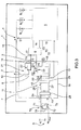
Figure 1 shows a schematic of an electric household appliance featuring an electronic device for reducing standby-mode energy consumption and in accordance with the teachings of the present invention; -
Figure 2 shows an electric diagram of the electronic device for reducing standby-mode energy consumption of theFigure 1 electric household appliance; -
Figure 3 shows an electric diagram of the electronic device for reducing standby-mode energy consumption of theFigure 1 electric household appliance in accordance with a variation of the present invention; -
Figure 4 shows a schematic of an oven featuring an electronic device for reducing standby-mode energy consumption of a display and in accordance with the teachings of the present invention; -
Figure 5 shows a schematic of an oven featuring a device for powering a display with low voltage and in accordance with a variation of the present invention. -
Number 1 inFigures 1 ,2 and3 indicates as a whole an electric household appliance (shown schematically) connected to anelectrical power network 3 comprising a neutral line N at a reference potential VREF corresponding to a neutral potential, and a phase line F at a phase potential V1. - In the example shown, potentials VREF and V1 of neutral line N and phase line F are set to obtain an alternating main supply voltage VA of roughly 220-230 V.
-
Appliance 1 comprises an electronic device (preferably a control unit) 5; and a low-voltage power unit 6 having an input connected toelectrical power network 3 to receive main supply voltage VA, and an output connected toelectronic device 5 to supply it with a low supply voltage VB, e.g. of about 4-12 volts. -
Appliance 1 also comprises adevice 7 for reducing the standby energy consumption ofappliance 1, and in turn comprising switching means 8, which are located along at least one of thepower lines 9 connecting low-voltage power unit 6 to phase line F and neutral line N ofelectrical power network 3, and operate between a closed state - in which they closepower line 9 to connect low-voltage power unit 6 toelectrical power network 3 and so turn on low-voltage power unit 6 and electronic device 5 - and an open state - in which they openpower line 9 to disconnect low-voltage power unit 6 fromelectrical power network 3 and so turn low-voltage power unit 6 andelectronic device 5 off completely. - Preferably, switching means 8 are switched from the open to the closed state by a low-voltage enabling signal S2, or from the closed to the open state by a disabling signal S3.
-
Device 7 also comprises, preferably, a low-voltagecapacitive power unit 10 input-connected toelectrical power network 3 to receive main supply voltage VA, and designed to generate low-voltage enabling signal S2 at the output. - In the
Figure 1 example,appliance 1 may be a washing machine, dishwasher, washer-dryer or drier, and comprises a number of known electric devices - hereinafter referred to simply as electric loads 2 - for performing the known washing/drying functions appliance 1 is designed for. - Being known electric/electronic devices,
electric loads 2 are not described, except to state that each has at least one power input connected to anelectrical power network 3 by aswitch 4 opened/closed by a control signal S1 to receive a main supply voltage VA fromelectrical power network 3. - In the
Figure 1 and2 example,electronic device 5 is a main electronic control unit 5 (for example a microprocessor) designed to control operation of eachelectric load 2 ofappliance 1, and, operable to generate control signal S1 to selectively disconnect eachelectric load 2 fromelectrical power network 3 when the washing/drying cycle is concluded and/or when theappliance 1 switches to a standby mode. -
Device 7 also comprises a hand-operatedcontrol device 11, e.g. a tactile switch or any other similar control device, connected between low-voltagecapacitive power unit 10 and switching means 8 to supply switching means 8 with low-voltage enabling signal S2. - Switching means 8 are designed to switch from the closed to the open state on receiving disabling signal S3 generated by main
electronic control unit 5 whenappliance 1 switches to standby mode, and to switch from the open to the closed state on receiving low-voltage enabling signal S2 generated by user operation ofcontrol device 11. - In the
Figure 1 and2 example, switching means 8 comprise twoinput terminals electrical power network 3; and twooutput terminals corresponding power terminals voltage power unit 6. - Switching means 8 also comprise a
first control input 18 connected to anoutput 19 of mainelectronic control unit 5 to receive disabling signal S3; and asecond control input 20 connected to the output terminal ofcontrol device 11 to receive enabling signal S2. - Preferably, switching means 8 comprise a
bistable relay 21, which has anelectric contact 22 movable between a first position associated with said open state and in which it openspower line 9 connecting low-voltage power unit 6 toelectrical power network 3, and a second position associated with said closed state and in which it closespower line 9 to connect low-voltage power unit 6 toelectrical power network 3. -
Bistable relay 21 also comprises anelectromagnetic device 23 comprising, for example, two coils for moving movableelectric contact 22 from the first to the second position on the basis of low-voltage enabling signal S2, or from the second to the first position on the basis of disabling signal S3. - In the
Figure 1 and2 example,electric contact 22 is interposed betweeninput terminal 12 andoutput terminal 14, so as to open/close them on command.Electromagnetic device 23, preferably, comprises a terminal connected tosecond control input 20 to receive low-voltage enabling signal S2; a terminal connected tofirst control input 18 to receive disabling signal S3; and a terminal connected toinput terminal 13. - Low-voltage
capacitive power unit 10, preferably, has aterminal 24 connected to phase line F; aterminal 25 connected to neutral line N; aterminal 26 connected bycontrol device 11 tosecond control input 20 of switching means 8; and aterminal 27 at a predetermined reference potential VREF preferably, though not necessarily, corresponding to the neutral potential. - Low-voltage
capacitive power unit 10 preferably comprises a capacitive dividingcircuit 28; and preferably a current-limitingcircuit 29 interposed between capacitive dividingcircuit 28 and switching means 8. - In the
Figure 2 circuit example,capacitive dividing circuit 28 comprises twoinput terminals terminals output terminals - Current-
limiting circuit 29, when envisaged, comprises, preferably, aninput terminal 34 connected bycontrol device 11 tooutput terminal 32 ofcapacitive dividing circuit 28; and anoutput terminal 35 connected tosecond control input 20 of switching means 8. - Preferably,
capacitive dividing circuit 28 comprises acapacitive divider 36 connected betweeninput terminals first capacitor 37 and asecond capacitor 38 connected in series betweeninput terminals common node 39. -
Capacitive dividing circuit 28 also preferably comprises a Zenerdiode 40 with the anode terminal connected toinput terminal 31, and the cathode terminal connected tonode 39; a third, preferably electrolytic,capacitor 41 connected betweenoutput terminals diode 42 with the anode terminal connected tonode 39, and the cathode terminal connected tooutput terminal 32. - In use, when capacitive dividing
circuit 28 is powered by the negative half-wave of supply voltage VA, Zenerdiode 40 conducts to only circulate a current I1 throughfirst capacitor 37, thus excludingsecond capacitor 38 andthird capacitor 41, which is therefore not charged at this stage. - It should be pointed out that, in the
Figure 2 example, the capacity C1 offirst capacitor 37 and the capacity C2 ofsecond capacitor 38 ofcapacitive divider 36 are advantageously such that, during the positive half-wave of supply voltage VA toterminals second capacitor 38 is lower than the Zener voltage VZ of Zenerdiode 40, which is therefore never reverse-biased. - Preferably, when capacitive dividing
circuit 28 is powered by the positive half-wave of supply voltage VA,capacitive divider 36 divides supply voltage VA to generate, at the terminals ofsecond capacitor 38, voltage VC2, which is lower than Zener voltage VZ of Zenerdiode 40, so that, at this stage, Zenerdiode 40 remains off, andthird capacitor 41 is charged with voltage VC3. - It should be pointed out that
first capacitor 37,second capacitor 38, andthird capacitor 41 together define, preferably, a reactive circuit, which is supplied as a whole with a current I1 having a predominantly capacitive component, which advantageously uses mainly reactive power. - Preferably, keeping
Zener diode 40 off during the positive half-wave of main supply voltage VA, a current I1 with a highly capacitive component is circulated, so that the power dissipated bycapacitive dividing circuit 28 is predominantly characterized by a reactive power component, and advantageously by a negligible active power component, thus resulting in extremely low active energy consumption of low-voltagecapacitive power unit 10 as a whole. - it should be pointed out that, unlike known capacitive pump circuits, in which the Zener diode must be reverse-biased during the positive half-wave of the main supply voltage to regulate the output voltage, capacitive dividing
circuit 28, preferably, serves solely to store energy by which to generate a signal and preferably and advantageously a pulse signal corresponding to low-voltage enabling signal S2 and of sufficient minimum energy to activatebistable relay 21. - In other words, capacitive dividing
circuit 28 does not need to regulate the output voltage VC3, but simply to generate a signal S2, preferably a pulse signal S2, to energize the coil ofbistable relay 21. Once activated, in fact,bistable relay 21 is designed to stay permanently in the last switch position, with no need for a constant, continuous electric input signal. - The circuit architecture achieved by
capacitive dividing circuit 28 supplyingbistable relay 21 with an enabling pulse signal S2 therefore greatly reduces the active energy dissipated bydevice 7, on account of the power/energy used bydevice 7 being predominantly reactive. - In the example shown, capacity C1 of
first capacitor 37 and C2 ofsecond capacitor 38 may be designed to satisfy the equation:
where VA is the peak value of main supply voltage VA; VC2 is the voltage at the terminals ofsecond capacitor 38; and VZ is the Zener voltage. - In the
Figure 1 and2 example,device 7 also comprises an EMC Filter 70 (Electro Magnetic Compatibility Filter) connected betweenbistable relay 21 and low-voltage power unit 6. -
EMC Filter 70 hasterminals power terminals voltage power unit 6 and comprises acapacitor 73 andbleeder resistor 74 designed to discharge thecapacitor 73. - Preferably,
capacitor 73 andbleeder resistor 74 are connected in parallel to each other betweenterminals - In accordance with a variation of the present invention shown in
Figure 3 ,EMC Filter 70 is interposed betweenelectrical power network 3 and low-voltagecapacitive power unit 10, i.e. upstream of thebistable relay 21. However in another alternative not shown, theEMC Filter 70 can be interposed between the low-voltagecapacitive power unit 10 and thebistable relay 21. - Preferably, according to variation shown in
Figure 3 ,terminals EMC Filter 70 are connected respectively toterminals capacitive power unit 10. - Operation of
device 7 to reduce the energy consumption ofappliance 1 will now be described, assumingappliance 1 is running, i.e. is not on standby mode, andbistable relay 21 is therefore in the closed position. - The
appliance 1 may be operable to automatically switch to standby mode after wash/dry cycle has been completed/ended, and/or, for example, whenelectronic device 5 does not receive any new user-commands within a prearranged time. - Main
electronic control unit 5 generates signal S1 to openswitch 4 and disconnectloads 2 fromelectrical power network 3, preferably when wash/dry cycle has been completed/ended and at the same time or later within a prearranged time generates disabling signal S3, which is preferably in the form of a pulse-type low voltage signal. - Disabling signal S3 switches
bistable relay 21 from closed to open, thus turning off low-voltage power unit 6 and mainelectronic control unit 5 at the same time. - It should be pointed out that, at this stage, unlike the energy consumption reducing systems of known appliances, the total energy consumption of low-
voltage power unit 6 and mainelectronic control unit 5 is advantageously nil. - This condition continues pending user operation/actuation of
control device 11. - In practice, user operation/actuation of
control device 11 supplies enabling signal S2 tobistable relay 21, which switches from open to closed to connect low-voltage power unit 6 toelectrical power network 3 and so turn on mainelectronic control unit 5. - Main
electronic control unit 5 may also be operable to advantageously enable user to turn off theappliance 1 by means of thecontrol device 11. - Main
electronic control unit 5 is, for this purpose designed, to detect whether user operates/actuatescontrol device 11 while the appliance is running -
Device 7 may comprise asensing device 44 for detecting low-voltage enabling signal S2 atsecond control input 20 ofbistable relay 21. -
Sensing device 44 may, for example, comprise a current/voltage measuring sensor for generating a logic signal indicating the presence/absence of low-voltage enabling signal S2 atsecond control input 20 ofbistable relay 21. - Preferably, main
electronic control unit 5 is designed to detect whether user operatescontrol device 11 on the basis of the logic state of the signal generated by sensingdevice 44. If user operatescontrol device 11 while the appliance is running, mainelectronic control unit 5 detect the logic state change of the signal generated by sensingdevice 44 corresponding to the presence of low-voltage enabling signal S2. - In this case, main
electronic control unit 5 determines the logic state signal change and generates signal S1 to openswitch 4 and disconnectloads 2 fromelectrical power network 3, and at the same time generates disabling signal S3, which is preferably in the form of a pulse-type low voltage signal. - Preferably, main
electronic control unit 5 may be operable to generate signals S1 and S3 when the signal/s generated by sensingdevice 44 meet/s prearranged conditions. - In accordance with a different embodiment, prearranged conditions may be met when the signal stays in a logic state for certain time interval.
- In accordance with an embodiment, prearranged condition may be met when logic state of the signal generated by sensing
device 44 changes a prearranged number of times within a certain temporal time interval. - Main
electronic control unit 5 may also be designed to advantageously detect power failure. - Preferably, main
electronic control unit 5 may be operable to determine power failure ofappliance 1, when low voltage VB is restored by the low-voltage main power unit in the absence of low-voltage enabling signal S2. - If power failure occurs while the appliance is running, switching means 8 remain closed, connecting low-voltage
main power unit 6 toelectrical power network 3; and, when power is restored, low-voltagemain power unit 6 is again powered to turn on mainelectronic control unit 5. - In this case, main
electronic control unit 5 determines whether it was turned on by power being restored, or by the user switchingbistable relay 21. - In the example shown, main
electronic control unit 5 determines whether the logic state of the signal generated by sensingdevice 44 corresponds to the presence of low-voltage enabling signal S2. - If the logic signal generated by sensing
device 44 indicates no low-voltage enabling signal S2, mainelectronic control unit 5 determines a power failure, and so controls loads 2 according to a program for reactivating the wash/dry cycle interrupted by the power failure. - Conversely, if the logic signal generated by sensing
device 44 indicates the presence of low-voltage enabling signal S2, mainelectronic control unit 5 determines no power failure, and so controls loads 2 according to a specific program for reactivating the user-selected wash cycle. - However alternative embodiments can be envisaged to enable the main
electronic control unit 5 to determine whether it was turned on by power being restored, or by the user switchingbistable relay 21, for example the mainelectronic control unit 5 can memorize at least the last step of the operating cycle running before the power failure, so that when the power is again available, thecontrol unit 5 can recognize that an interruption has occurred and control theloads 2 accordingly for reactivating, for example, the wash/dry cycle interrupted by the power failure or thecontrol unit 5 can proceed with specific program sequences envisaged in case of operating cycle interruption. -
Electric household appliance 1 described has the following advantages: - Firstly, total standby energy consumption of the low-voltage power unit and main
electronic control unit 5 is nil. - Secondly, using a bistable relay controlled by two distinct pulse signals enables use of a low-voltage capacitive power unit with simpler circuitry than conventional capacitive pumps. In fact, unlike conventional capacitive pumps, in which the Zener diode is reverse-biased to regulate the output voltage, appropriately designing the first and second capacitors of the capacitive dividing circuit, previously described, prevents reverse biasing of the Zener diode, which therefore simply acts as a voltage limiter.
- Thirdly, the configuration of the capacitive dividing circuit greatly reduces active power consumption in standby mode. That is, as stated, the current circulating in the capacitive dividing circuit has a predominantly capacitive component which obviously dissipates reactive power.
- Finally, using a bistable relay that permanently maintains its operating state enables power failure detection by the electronic control unit.
- Clearly, changes may be made to the electric household appliance as described and illustrated herein without, however, departing from the scope of the present invention.
- For example in another alternative, depicted as an example in
figure 4 , the electric household appliance comprises display means, a voltage supply control unit for supplying an electric voltage to said display means and sensor switching means which turn on/off the low-voltage power unit according to detection of user within a given distance from the appliance, electric household appliance further comprises a device for reducing energy consumption of the electric household appliance comprising low-voltage capacitive power means designed to supply a low-voltage to said sensor switching means. - Preferably, the low-voltage capacitive power means comprises a capacitive dividing circuit comprising a first and second input terminal connected to a first and second power line at a first and second predetermined potential respectively; a first and second output terminals generating said low-voltage; first and second charge-accumulating means connected between said first and second input terminal; and at least one voltage limiter connected parallel to said second charge-accumulating means and designed to switch from a non-conducting to a conducting state when subjected to a voltage above a predetermined breakdown voltage; said first and second charge-accumulating means being so designed that the voltage at the terminals of said second charge-accumulating means is below said predetermined breakdown voltage.
- Preferably, the capacitive dividing circuit comprises third charge-accumulating means connected between said first and second output terminal.
- Preferably, the voltage limiter comprises a Zener diode having the anode and cathode terminals connected respectively to the input terminal of said capacitive dividing circuit and to a node between said first and second charge-accumulating means. Preferably, the first, second, and third charge-accumulating means respectively comprise a first, second, and third capacitor designed according to the equation:

where VA is the peak value of the main supply voltage; VC2 is the voltage at the terminals of the second capacitor; and VZ is the Zener voltage. - Preferably, the low-voltage capacitive power means comprise voltage regulating means interposed between said capacitive dividing circuit and said sensor switching means.
- More in detail, the
Figure 4 embodiment relates to anoven 50 comprising adisplay 52, preferably, though not necessarily a clock display; adevice 51 for reducing energy consumption ofdisplay 52 whenoven 50 is on standby and unattended by the user; and preferably, though not necessary, avoltage power unit 80 having an input connected toelectrical power network 3 to receive main supply voltage VA, and an output connected to display 52 to supply it with a secondary supply voltage VB. - In
Figure 4 ,device 51 for reducing energy consumption ofdisplay 52 comprises switching means 81, which are located along at least one of thepower lines 82 connectingvoltage power unit 80 to phase line F and neutral line N ofelectrical power network 3, and operate between a closed state - in which they closepower line 82 to connectvoltage power unit 80 toelectrical power network 3 and so turn onvoltage power unit 80 and display 52 - and an open state - in which they openpower line 82 to disconnectvoltage power unit 80 fromelectrical power network 3 and so turnvoltage power unit 80 anddisplay 52 off completely. - Preferably, switching means 81 are switched from the open to the closed state by a low-voltage enabling signal S2, or from the closed to the open state by a disabling signal S3.
-
Device 51 also comprises a low-voltagecapacitive power unit 83 input-connected toelectrical power network 3 to receive main supply voltage VA, and designed to generate a low voltage V2 at the output. -
Device 51 also comprises aproximity sensor 90 for detecting the presence or absence of the user within a given distance fromoven 50. - Preferably,
proximity sensor 90 is connected to the output of low-voltagecapacitive power unit 83, preferably, though not necessary, via a knownvoltage regulating device 84, and is designed to output enabling signal S2 when the user is within a given distance fromoven 50, and, conversely, to output a disabling signal S3 when the user is not within a given distance fromoven 50. - Switching means 81 are designed to switch from the closed to the open state on receiving disabling signal S3 when user is not within a given distance from
oven 50, and to switch from the open to the closed state on receiving low-voltage enabling signal S2 when the user is within a given distance fromoven 50. - In the
Figure 4 , switching means 81 comprise twoinput terminals electrical power network 3; and twooutput terminals corresponding power terminals voltage power unit 80. - Switching means 81 also comprise a
first control input 100 connected to a first output ofproximity sensor 90 to receive disabling signal S3; and asecond control input 98 connected to a second output terminal ofproximity sensor 90 to receive enabling signal S2. - Preferably, switching means 81 comprise a
bistable relay 101, which has anelectric contact 102 movable between a first position associated with said open state and in which it openspower line 82 connectingvoltage power unit 80 toelectrical power network 3, and a second position associated with said closed state and in which it closespower line 82 to connectvoltage power unit 80 toelectrical power network 3. -
Bistable relay 101 also comprises anelectromagnetic device 103 comprising, for example, two coils for moving movableelectric contact 102 from the first to the second position on the basis of enabling signal S2, or from the second to the first position on the basis of disabling signal S3. - In the
Figure 4 example,electric contact 102 is interposed betweeninput terminal 92 andoutput terminal 94, so as to open/close them on command. Andelectromagnetic device 103 has a terminal connected tosecond control input 98 to receive low-voltage enabling signal S2; a terminal connected tofirst control input 100 to receive disabling signal S3; and a terminal connected to input terminal 93. - Low-voltage
capacitive power unit 83 has a terminal 104 connected to phase line F; a terminal 105 connected to neutral line N; a terminal 106 connected toproximity sensor device 90; and a terminal 107 at a predetermined reference potential VREF preferably, though not necessarily, corresponding to the neutral potential. - Low-voltage
capacitive power unit 83 substantially comprises acapacitive dividing circuit 108; whereas regulatingdevice 84, when envisaged, is interposed between capacitive dividingcircuit 108 andproximity sensor 90. - In the
Figure 4 circuit example, capacitive dividingcircuit 108 comprises twoinput terminals terminals output terminals - Regulating
device 84 comprises aninput terminal 114 connected tooutput terminal 112 ofcapacitive dividing circuit 108; and anoutput terminal 115 connected toproximity sensor 90 to supply low-voltage V2. - Preferably, capacitive dividing
circuit 108 comprises acapacitive divider 116 connected betweeninput terminals first capacitor 117 and asecond capacitor 118 connected in series betweeninput terminals common node 119. - Capacitive dividing
circuit 108 also comprises aZener diode 120 with the anode terminal connected to input terminal 111, and the cathode terminal connected tonode 119; a third, preferably electrolytic,capacitor 121 connected betweenoutput terminals diode 122 with the anode terminal connected tonode 119, and the cathode terminal connected tooutput terminal 112. - In the
Figure 4 ,device 51 can also comprises an EMC Filter 200 (Electro Magnetic Compatibility Filter) which is interposed betweenbistable relay 101 andvoltage power unit 80. -
EMC Filter 200 has two terminals which are connected respectively topower terminals voltage power unit 80 and comprises acapacitor 203 and ableeder resistor 204 designed to discharge thecapacitor 203. - Preferably,
capacitor 203 andbleeder resistor 204 are connected in parallel to each other. - In accordance with a variation of the present invention (not shown),
EMC Filter 200 is interposed betweenelectrical power network 3 and low-voltagecapacitive power unit 83, i.e. upstream thebistable relay 21. - Preferably, according to variation, terminals of the
EMC Filter 200 are connected respectively toterminals capacitive power unit 83. - In use, when
capacitive dividing circuit 108 is powered by the negative half-wave of supply voltage VA,Zener diode 120 conducts to only circulate a current I1 throughfirst capacitor 117, thus excludingsecond capacitor 118 andthird capacitor 121, which is therefore not charged at this stage. - It should be pointed out that, in the
Figure 4 example, the capacity C1 offirst capacitor 117 and the capacity C2 ofsecond capacitor 118 ofcapacitive divider 116 are advantageously such that, during the positive half-wave of supply voltage VA toterminals second capacitor 118 is lower than the Zener voltage VZ ofZener diode 120, which is therefore never reverse-biased. - Preferably, when
capacitive dividing circuit 108 is powered by the positive half-wave of supply voltage VA,capacitive divider 116 divides supply voltage VA to generate, at the terminals ofsecond capacitor 118, voltage VC2, which is lower than Zener voltage VZ ofZener diode 120, so that, at this stage,Zener diode 120 remains off, andthird capacitor 121 is charged with voltage VC3. - It should be pointed out that
first capacitor 117,second capacitor 118, andthird capacitor 121 together define a reactive circuit, which is supplied as a whole with a current I1 having a predominantly capacitive component, which advantageously provides/uses mainly reactive power. - Preferably, keeping
Zener diode 120 off during the positive half-wave of main supply voltage VA, a current I1 with a highly capacitive component is circulated, so the power dissipated bycapacitive dividing circuit 108 is predominantly characterized by a reactive power component, and advantageously by a negligible active power component, thus resulting in extremely low active energy consumption of low-voltagecapacitive power unit 83 as a whole. - It should be pointed out that, unlike known capacitive pump circuits, in which the
Zener diode 120 must be reverse-biased during the positive half-wave of the main supply voltage to regulate the output voltage, capacitive dividingcircuit 108 serves solely to store sufficient minimum energy by which to supply theproximity sensor 90. - The circuit architecture achieved by
capacitive dividing circuit 108 supplyingproximity sensor 90 therefore greatly reduces the active energy dissipated bydevice 51, on account of the power/energy provided/used bydevice 51 being predominantly reactive. - In the example shown, capacity C1 of
first capacitor 117 and C2 ofsecond capacitor 118 may be designed to satisfy the equation:
where VA is the peak value of main supply voltage VA; VC2 is the voltage at the terminals ofsecond capacitor 118; and VZ is the Zener voltage. - In actual use, when the user is within a given distance from
oven 50,proximity sensor 90 generates enabling signal S2 to switch movableelectric contact 102 ofbistable relay 101 into the second operating position and so turn onvoltage power unit 80 anddisplay 52. - Conversely, when the user is not within a given distance from
oven 50,proximity sensor 90 generates disabling signal S3 to switch movableelectric contact 102 into the first operating position and so turn offvoltage power unit 80 anddisplay 52. - In another alternative, depicted as an example in
figure 5 , the electric household appliance comprises display means, voltage power means connected to an electrical power network to receive a main supply voltage to supply a voltage to said display means, a device for reducing energy consumption comprising: - switching means which are switched by a enabling signal to a closed state connecting said voltage power means to the electrical power network to turn on the voltage power means and said display means;
- a proximity sensor generating said enabling signal when detects a user within a given distance from the appliance; and
- low-voltage capacitive power means which supply a low-voltage to supply said proximity sensor.
- Preferably, the proximity sensor outputs a disabling signal when does not detect a user within said given distance from the appliance; said switching means being switched by the disabling signal to an open state disconnecting voltage power means from the electrical power network to turn the voltage power means and said display means off completely.
- Preferably, the switching means comprise a bistable relay.
- Preferably, the bistable relay comprises at least one movable electric contact movable between a first position associated with said open state and wherein it opens a power line connecting said voltage power means to a electrical power network, and a second position associated with said closed state and wherein it closes said power line.
- Preferably, the bistable relay comprises electromagnetic means designed to move said movable electric contact from the first to the second position on the basis of the enabling signal, or to move the movable electric contact from the second to the first position on the basis of the disabling signal.
- Preferably, the low-voltage capacitive power means comprises a capacitive dividing circuit comprising a first and second input terminal connected to a first and second power line at a first and second predetermined potential respectively; a first and second output terminals generating said low-voltage; first and second charge-accumulating means connected between said first and second input terminal; and at least one voltage limiter connected parallel to said second charge-accumulating means and designed to switch from a non-conducting to a conducting state when subjected to a voltage above a predetermined breakdown voltage; said first and second charge-accumulating means being so designed that the voltage at the terminals of said second charge-accumulating means is below said predetermined breakdown voltage.
- Preferably, the capacitive dividing circuit comprises third charge-accumulating means connected between said first and second output terminal.
- Preferably, the voltage limiter comprises a Zener diode having the anode and cathode terminals connected respectively to the input terminal of said capacitive dividing circuit and to a node between said first and second charge-accumulating means.
- Preferably, the first, second, and third charge-accumulating means respectively comprise a first, second, and third capacitor designed according to the equation:

where VA is the peak value of the main supply voltage; VC2 is the voltage at the terminals of the second capacitor; and VZ is the Zener voltage. - Preferably, the low-voltage capacitive power means comprise voltage regulating means interposed between said capacitive dividing circuit and said sensor switching means.
- Preferably, the electric household appliance comprises an EMC Filter which is interposed between outputs of said switching means and input of said voltage power means.
- Preferably, the electric household appliance comprises an EMC Filter being connected to the first and second input terminal of said capacitive dividing circuit.
- More in detail,
Figure 5 shows analternative device 130 for reducing energy consumption of adisplay 131 of anoven 50, for example, and which is similar todevice 51, and the component parts of which are indicated, where possible, using the same reference numbers as for the corresponding parts ofdevice 51. -
Device 130 differs fromdevice 51 bydisplay 131 being connected by apower control unit 132 to theelectrical power network 3 to receive supply voltage. - Moreover,
device 130 has not switching means. - In detail,
power control unit 132 comprisescontrol inputs outputs proximity sensor 90 to receive enabling signal S2 and disabling signal S3, and is operable to switched from no-power supply state to a power supply state by the enabling signal S2, or from power supply state to no-power supply state by the disabling signal S3. - More specifically, on receiving disabling signal S3
power control unit 132 cuts off electrical power supply to display 131. In other words, disabling signal S3 commandspower control unit 132 so as to turning off to display 131. - On receiving enabling signal S2,
power control unit 132 supply electrical power to turn on thedisplay 131.
Claims (6)
- Electric household appliance (1) comprising display means (52), a voltage supply control unit (81) for supplying an electric voltage to said display means (52) and sensor switching means (90) which turn on/off a low-voltage power unit (80) according to detection of a user within a given distance from the appliance (1), wherein the electric household appliance (1) further comprises a device for reducing energy consumption of the electric household appliance comprising low-voltage capacitive power means (83) designed to supply a low-voltage (V2) to said sensor switching means (90).
- Electric household appliance as claimed in claim 1, wherein the low-voltage capacitive power means (83) comprises at least one of the following features:- a capacitive dividing circuit (108) comprising a first (110) and second (111) input terminal connected to a first (104) and second (105) power line at a first and second predetermined potential respectively;- a first (106) and second (107) output terminal generating said low-voltage (V2);- first (117) and second (118) charge-accumulating means connected between said first (110) and second (111) input terminal; and- at least one voltage limiter (120) connected parallel to said second charge-accumulating means (118) and designed to switch from a non-conducting to a conducting state when subjected to a voltage above a predetermined breakdown voltage;- said first (117) and second (118) charge-accumulating means being so designed that the voltage at the terminals of said second charge-accumulating means is below said predetermined breakdown voltage.
- Electric household appliance as claimed in claims 1 or 2, wherein the capacitive dividing circuit (108) comprises third charge-accumulating means (121) connected between said first (106) and second (107) output terminal.
- Electric household appliance as claimed in any one of the foregoing claims, wherein the voltage limiter (121) comprises a Zener diode having the anode and cathode terminals connected respectively to the input terminal (111) of said capacitive dividing circuit (108) and to a node (119) between said first (117) and second (118) charge-accumulating means.
- Electric household appliance as claimed in any one of the foregoing claims, wherein the first (117), second (118), and third (121) charge-accumulating means respectively comprise a first (C1), second (C2), and third (C3) capacitor designed according to the equation
VA*(2*C1)/(C2+C1)-0.7=VC2≤VZ
where VA is the peak value of the main supply voltage; VC2 is the voltage at the terminals of the second capacitor; and VZ is the Zener voltage. - Electric household appliance as claimed in any one of the foregoing claims, the low-voltage capacitive power means (83) comprise voltage regulating means (84) interposed between said capacitive dividing circuit (108) and said sensor switching means (90).
Priority Applications (1)
| Application Number | Priority Date | Filing Date | Title |
|---|---|---|---|
| EP11184977.4A EP2407850B1 (en) | 2010-03-30 | 2010-03-30 | Household appliance circuit arrangement |
Applications Claiming Priority (2)
| Application Number | Priority Date | Filing Date | Title |
|---|---|---|---|
| EP10158335.9A EP2372488B1 (en) | 2010-03-30 | 2010-03-30 | Household appliance circuit arrangement |
| EP11184977.4A EP2407850B1 (en) | 2010-03-30 | 2010-03-30 | Household appliance circuit arrangement |
Related Parent Applications (2)
| Application Number | Title | Priority Date | Filing Date |
|---|---|---|---|
| EP10158335.9 Division | 2010-03-30 | ||
| EP10158335.9A Division EP2372488B1 (en) | 2010-03-30 | 2010-03-30 | Household appliance circuit arrangement |
Publications (2)
| Publication Number | Publication Date |
|---|---|
| EP2407850A1 true EP2407850A1 (en) | 2012-01-18 |
| EP2407850B1 EP2407850B1 (en) | 2015-06-17 |
Family
ID=42556526
Family Applications (3)
| Application Number | Title | Priority Date | Filing Date |
|---|---|---|---|
| EP10158335.9A Active EP2372488B1 (en) | 2010-03-30 | 2010-03-30 | Household appliance circuit arrangement |
| EP11184977.4A Not-in-force EP2407850B1 (en) | 2010-03-30 | 2010-03-30 | Household appliance circuit arrangement |
| EP11184986.5A Not-in-force EP2407851B1 (en) | 2010-03-30 | 2010-03-30 | Household appliance circuit arrangement |
Family Applications Before (1)
| Application Number | Title | Priority Date | Filing Date |
|---|---|---|---|
| EP10158335.9A Active EP2372488B1 (en) | 2010-03-30 | 2010-03-30 | Household appliance circuit arrangement |
Family Applications After (1)
| Application Number | Title | Priority Date | Filing Date |
|---|---|---|---|
| EP11184986.5A Not-in-force EP2407851B1 (en) | 2010-03-30 | 2010-03-30 | Household appliance circuit arrangement |
Country Status (6)
| Country | Link |
|---|---|
| US (1) | US9647490B2 (en) |
| EP (3) | EP2372488B1 (en) |
| CN (1) | CN102870060B (en) |
| BR (1) | BR112012024562B1 (en) |
| RU (1) | RU2533501C2 (en) |
| WO (1) | WO2011120958A1 (en) |
Families Citing this family (7)
| Publication number | Priority date | Publication date | Assignee | Title |
|---|---|---|---|---|
| EP2372493B1 (en) * | 2010-03-30 | 2020-05-13 | Electrolux Home Products Corporation N.V. | Device for reducing standby-mode energy consumption of an electric household appliance |
| EP2434613B1 (en) | 2010-09-28 | 2018-02-21 | Electrolux Home Products Corporation N.V. | Electronic control device and method for reducing stand-by state energy consumption of an electric household appliance |
| EP2589973A1 (en) * | 2011-11-03 | 2013-05-08 | Electrolux Home Products Corporation N.V. | Ground power leakage detection for peripheral printed circuit boards |
| EP2784523B1 (en) * | 2013-03-28 | 2020-02-19 | Electrolux Appliances Aktiebolag | Method and circuit for determining dispersion of electric power towards ground in electric appliances |
| US10320202B2 (en) * | 2014-09-30 | 2019-06-11 | Johnson Controls Technology Company | Battery system bi-stable relay control |
| US10353558B2 (en) | 2016-01-13 | 2019-07-16 | Electrolux Home Products, Inc. | Drag-and-set user interface for appliances |
| CN107179461A (en) * | 2017-06-20 | 2017-09-19 | 浙江吉利汽车有限公司 | Efp detection means and power supply unit |
Citations (2)
| Publication number | Priority date | Publication date | Assignee | Title |
|---|---|---|---|---|
| GB2411278A (en) * | 2004-02-20 | 2005-08-24 | Pelikon Ltd | Display activated by presence of user |
| DE102006054539B3 (en) | 2006-11-20 | 2008-02-14 | BSH Bosch und Siemens Hausgeräte GmbH | Generating low voltage power supply for washing machine controller, employs power supply unit switched by separate capacitor power supply and program selector switch |
Family Cites Families (44)
| Publication number | Priority date | Publication date | Assignee | Title |
|---|---|---|---|---|
| US3603732A (en) | 1969-06-05 | 1971-09-07 | Rca Corp | Instant-on circuitry for solid state television receivers |
| US3641393A (en) * | 1971-01-25 | 1972-02-08 | Douglas A Florance | Automatic ground fault circuit interrupter |
| US3831065A (en) | 1973-04-06 | 1974-08-20 | Integrated Conversion Tech | Electronic push button combination lock |
| US4015171A (en) | 1976-02-06 | 1977-03-29 | International Telephone And Telegraph Corporation | Resettable overcurrent-protected direct current power supply |
| US4665355A (en) * | 1986-09-15 | 1987-05-12 | Rockwell International Corporation | Off line capacitor-divider power supply for solid state power controller |
| DE4029543C2 (en) * | 1990-09-18 | 1994-09-29 | Bosch Siemens Hausgeraete | Safety device for water-bearing household appliances, in particular household dishwashers |
| US5387848A (en) * | 1992-03-05 | 1995-02-07 | Philips Electronics North America Corporation | Fluorescent lamp ballast with regulated feedback signal for improved power factor |
| US5453921A (en) | 1993-03-31 | 1995-09-26 | Thomson Consumer Electronics, Inc. | Feedback limited duty cycle switched mode power supply |
| US5525948A (en) | 1994-12-02 | 1996-06-11 | Poulsen; Peder U. | Manually operated, electromagnetically resettable safety switch |
| KR0164814B1 (en) | 1995-01-23 | 1999-02-01 | 김광호 | Voltage driving circuit of semiconductor memory apparatus |
| KR100199831B1 (en) * | 1996-01-15 | 1999-06-15 | 구자홍 | Power saving control circuit of a image displayer |
| US5926394A (en) | 1996-09-30 | 1999-07-20 | Intel Corporation | Method and apparatus for regulating the voltage supplied to an integrated circuit |
| GB9623612D0 (en) | 1996-11-13 | 1997-01-08 | Rca Thomson Licensing Corp | Separate power supplies for standby operation |
| US5961207A (en) * | 1997-06-16 | 1999-10-05 | Petkovic; Peter M. | Trouble light apparatus |
| KR19990078513A (en) | 1998-12-16 | 1999-11-05 | 김형광 | Auto power switchgear |
| DE19943124A1 (en) | 1999-09-09 | 2001-03-15 | Bsh Bosch Siemens Hausgeraete | Device for detecting a power failure in a program-controlled household appliance |
| JP2001145355A (en) | 1999-11-11 | 2001-05-25 | Lg Electronics Inc | Stand-by power reducing circuit for electric equipment |
| JP2001145170A (en) | 1999-11-15 | 2001-05-25 | Nikon Gijutsu Kobo:Kk | Standby power saving electrical apparatus |
| KR100376131B1 (en) | 2000-09-22 | 2003-03-15 | 삼성전자주식회사 | Consumption power saving apparatus and controlling method in a stand-by mode |
| US6724220B1 (en) | 2000-10-26 | 2004-04-20 | Cyress Semiconductor Corporation | Programmable microcontroller architecture (mixed analog/digital) |
| EP1211895A1 (en) | 2000-11-30 | 2002-06-05 | Deutsche Thomson-Brandt Gmbh | Circuit arrangement for processing a band of digital television channels |
| DE10106132A1 (en) | 2001-02-10 | 2002-08-14 | Philips Corp Intellectual Pty | Wake-up circuit for an electrical device |
| US6995807B2 (en) | 2001-11-02 | 2006-02-07 | Sony Corporation | Micro-power stand-by mode |
| US20050041360A1 (en) | 2003-08-20 | 2005-02-24 | E.G.O. North America, Inc. | Systems and methods for achieving low power standby through interaction between a microcontroller and a switching mode power supply |
| JP2005312174A (en) * | 2004-04-21 | 2005-11-04 | Sharp Corp | Power supply controller and washing machine having the same |
| CN100359418C (en) | 2004-07-05 | 2008-01-02 | 周先谱 | Control device of zero power consumption readiness power source |
| US7840142B2 (en) | 2004-07-23 | 2010-11-23 | Thomson Licensing | System and method for reducing standby power consumption |
| JP2006072257A (en) | 2004-09-06 | 2006-03-16 | Ricoh Co Ltd | Image forming apparatus |
| GB0500183D0 (en) | 2005-01-07 | 2005-02-16 | Koninkl Philips Electronics Nv | Switched mode power supply |
| US7714265B2 (en) * | 2005-09-30 | 2010-05-11 | Apple Inc. | Integrated proximity sensor and light sensor |
| CA2523166A1 (en) | 2005-10-11 | 2007-04-11 | Indigo Manufacturing Inc. | Audio signal detection utilizing low power standby power supply |
| JP2008054085A (en) | 2006-08-25 | 2008-03-06 | Hitachi Ltd | Broadcast receiving apparatus and starting method thereof |
| CN201017251Y (en) * | 2007-04-04 | 2008-02-06 | 张亦翔 | Electric capacity voltage dividing type DC voltage-stabilized power supply |
| US20090021969A1 (en) | 2007-07-20 | 2009-01-22 | Richard George Arthur Butler | Appliance and power supply therefor |
| US7944086B2 (en) * | 2007-10-18 | 2011-05-17 | Hammerhead International, Llc | System and method for load control |
| US7808219B2 (en) * | 2007-11-26 | 2010-10-05 | Honeywell International Inc. | Method and apparatus of capacitor divider based offline AC-DC converter |
| DE102008011279A1 (en) | 2007-12-03 | 2009-06-10 | Fujitsu Siemens Computers Gmbh | Electrical device i.e. computer, for use in e.g. office, has power supply unit shifted from hard-off mode into on-mode and vice versa, where electrical device operates control device in hard-off mode independent of supply network |
| US7948283B2 (en) | 2008-01-23 | 2011-05-24 | Tritan Technology Inc. | Apparatus for awaking an electronic device from a standby mode |
| US7779278B2 (en) | 2008-05-29 | 2010-08-17 | Igo, Inc. | Primary side control circuit and method for ultra-low idle power operation |
| US8898486B2 (en) | 2009-06-01 | 2014-11-25 | Lg Electronics Inc. | Apparatus and method for controlling input power |
| US8416553B2 (en) | 2009-10-30 | 2013-04-09 | Intersil Americas Inc. | Bias and discharge system for low power loss start up and input capacitance discharge |
| US8421275B2 (en) | 2009-11-19 | 2013-04-16 | Electrolux Home Products, Inc. | Apparatus for providing zero standby power control in an appliance |
| US8624430B2 (en) | 2009-11-19 | 2014-01-07 | General Electric Company | Standby power reduction |
| EP2434611B1 (en) | 2010-09-28 | 2016-03-02 | Electrolux Home Products Corporation N.V. | Electronic control device and method for reducing stand-by state energy consumption of an electric household appliance |
-
2010
- 2010-03-30 EP EP10158335.9A patent/EP2372488B1/en active Active
- 2010-03-30 EP EP11184977.4A patent/EP2407850B1/en not_active Not-in-force
- 2010-03-30 EP EP11184986.5A patent/EP2407851B1/en not_active Not-in-force
-
2011
- 2011-03-29 BR BR112012024562-7A patent/BR112012024562B1/en active IP Right Grant
- 2011-03-29 US US13/637,821 patent/US9647490B2/en active Active
- 2011-03-29 CN CN201180022072.0A patent/CN102870060B/en active Active
- 2011-03-29 RU RU2012146122/08A patent/RU2533501C2/en not_active IP Right Cessation
- 2011-03-29 WO PCT/EP2011/054805 patent/WO2011120958A1/en active Application Filing
Patent Citations (2)
| Publication number | Priority date | Publication date | Assignee | Title |
|---|---|---|---|---|
| GB2411278A (en) * | 2004-02-20 | 2005-08-24 | Pelikon Ltd | Display activated by presence of user |
| DE102006054539B3 (en) | 2006-11-20 | 2008-02-14 | BSH Bosch und Siemens Hausgeräte GmbH | Generating low voltage power supply for washing machine controller, employs power supply unit switched by separate capacitor power supply and program selector switch |
Also Published As
| Publication number | Publication date |
|---|---|
| RU2012146122A (en) | 2014-05-10 |
| EP2407850B1 (en) | 2015-06-17 |
| BR112012024562A2 (en) | 2020-08-11 |
| EP2407851A1 (en) | 2012-01-18 |
| BR112012024562B1 (en) | 2021-04-20 |
| EP2372488B1 (en) | 2013-08-07 |
| CN102870060B (en) | 2014-12-31 |
| WO2011120958A1 (en) | 2011-10-06 |
| US9647490B2 (en) | 2017-05-09 |
| CN102870060A (en) | 2013-01-09 |
| EP2407851B1 (en) | 2018-08-08 |
| US20130062968A1 (en) | 2013-03-14 |
| RU2533501C2 (en) | 2014-11-20 |
| EP2372488A1 (en) | 2011-10-05 |
Similar Documents
| Publication | Publication Date | Title |
|---|---|---|
| EP2407851B1 (en) | Household appliance circuit arrangement | |
| US9906026B2 (en) | Device for reducing standby-mode energy consumption of an electric household appliance | |
| EP2434613B1 (en) | Electronic control device and method for reducing stand-by state energy consumption of an electric household appliance | |
| CN103210563B (en) | For reducing control electronics and the method for the stand-by state energy consumption of household electrical appliance | |
| EP2622711B1 (en) | Electronic control device and method for reducing stand-by state energy consumption of an electric household appliance | |
| EP2722965A1 (en) | Electronic control device and method for reducing stand-by state energy consumption of an electric household appliance | |
| RU2575692C2 (en) | Device for reduction of power consumption by electrical household appliance in standby mode |
Legal Events
| Date | Code | Title | Description |
|---|---|---|---|
| 17P | Request for examination filed |
Effective date: 20111130 |
|
| AC | Divisional application: reference to earlier application |
Ref document number: 2372488 Country of ref document: EP Kind code of ref document: P |
|
| AK | Designated contracting states |
Kind code of ref document: A1 Designated state(s): AT BE BG CH CY CZ DE DK EE ES FI FR GB GR HR HU IE IS IT LI LT LU LV MC MK MT NL NO PL PT RO SE SI SK SM TR |
|
| AX | Request for extension of the european patent |
Extension state: AL BA ME RS |
|
| PUAI | Public reference made under article 153(3) epc to a published international application that has entered the european phase |
Free format text: ORIGINAL CODE: 0009012 |
|
| 17Q | First examination report despatched |
Effective date: 20120904 |
|
| GRAP | Despatch of communication of intention to grant a patent |
Free format text: ORIGINAL CODE: EPIDOSNIGR1 |
|
| INTG | Intention to grant announced |
Effective date: 20150317 |
|
| GRAS | Grant fee paid |
Free format text: ORIGINAL CODE: EPIDOSNIGR3 |
|
| GRAA | (expected) grant |
Free format text: ORIGINAL CODE: 0009210 |
|
| AC | Divisional application: reference to earlier application |
Ref document number: 2372488 Country of ref document: EP Kind code of ref document: P |
|
| AK | Designated contracting states |
Kind code of ref document: B1 Designated state(s): AT BE BG CH CY CZ DE DK EE ES FI FR GB GR HR HU IE IS IT LI LT LU LV MC MK MT NL NO PL PT RO SE SI SK SM TR |
|
| REG | Reference to a national code |
Ref country code: GB Ref legal event code: FG4D |
|
| REG | Reference to a national code |
Ref country code: CH Ref legal event code: EP |
|
| REG | Reference to a national code |
Ref country code: AT Ref legal event code: REF Ref document number: 732255 Country of ref document: AT Kind code of ref document: T Effective date: 20150715 |
|
| REG | Reference to a national code |
Ref country code: IE Ref legal event code: FG4D |
|
| REG | Reference to a national code |
Ref country code: DE Ref legal event code: R096 Ref document number: 602010025369 Country of ref document: DE |
|
| PG25 | Lapsed in a contracting state [announced via postgrant information from national office to epo] |
Ref country code: HR Free format text: LAPSE BECAUSE OF FAILURE TO SUBMIT A TRANSLATION OF THE DESCRIPTION OR TO PAY THE FEE WITHIN THE PRESCRIBED TIME-LIMIT Effective date: 20150617 Ref country code: FI Free format text: LAPSE BECAUSE OF FAILURE TO SUBMIT A TRANSLATION OF THE DESCRIPTION OR TO PAY THE FEE WITHIN THE PRESCRIBED TIME-LIMIT Effective date: 20150617 Ref country code: LT Free format text: LAPSE BECAUSE OF FAILURE TO SUBMIT A TRANSLATION OF THE DESCRIPTION OR TO PAY THE FEE WITHIN THE PRESCRIBED TIME-LIMIT Effective date: 20150617 Ref country code: NO Free format text: LAPSE BECAUSE OF FAILURE TO SUBMIT A TRANSLATION OF THE DESCRIPTION OR TO PAY THE FEE WITHIN THE PRESCRIBED TIME-LIMIT Effective date: 20150917 |
|
| REG | Reference to a national code |
Ref country code: AT Ref legal event code: MK05 Ref document number: 732255 Country of ref document: AT Kind code of ref document: T Effective date: 20150617 |
|
| REG | Reference to a national code |
Ref country code: LT Ref legal event code: MG4D Ref country code: NL Ref legal event code: MP Effective date: 20150617 |
|
| PG25 | Lapsed in a contracting state [announced via postgrant information from national office to epo] |
Ref country code: GR Free format text: LAPSE BECAUSE OF FAILURE TO SUBMIT A TRANSLATION OF THE DESCRIPTION OR TO PAY THE FEE WITHIN THE PRESCRIBED TIME-LIMIT Effective date: 20150918 Ref country code: BG Free format text: LAPSE BECAUSE OF FAILURE TO SUBMIT A TRANSLATION OF THE DESCRIPTION OR TO PAY THE FEE WITHIN THE PRESCRIBED TIME-LIMIT Effective date: 20150917 Ref country code: LV Free format text: LAPSE BECAUSE OF FAILURE TO SUBMIT A TRANSLATION OF THE DESCRIPTION OR TO PAY THE FEE WITHIN THE PRESCRIBED TIME-LIMIT Effective date: 20150617 |
|
| PG25 | Lapsed in a contracting state [announced via postgrant information from national office to epo] |
Ref country code: EE Free format text: LAPSE BECAUSE OF FAILURE TO SUBMIT A TRANSLATION OF THE DESCRIPTION OR TO PAY THE FEE WITHIN THE PRESCRIBED TIME-LIMIT Effective date: 20150617 |
|
| PG25 | Lapsed in a contracting state [announced via postgrant information from national office to epo] |
Ref country code: RO Free format text: LAPSE BECAUSE OF NON-PAYMENT OF DUE FEES Effective date: 20150617 Ref country code: SK Free format text: LAPSE BECAUSE OF FAILURE TO SUBMIT A TRANSLATION OF THE DESCRIPTION OR TO PAY THE FEE WITHIN THE PRESCRIBED TIME-LIMIT Effective date: 20150617 Ref country code: CZ Free format text: LAPSE BECAUSE OF FAILURE TO SUBMIT A TRANSLATION OF THE DESCRIPTION OR TO PAY THE FEE WITHIN THE PRESCRIBED TIME-LIMIT Effective date: 20150617 Ref country code: PT Free format text: LAPSE BECAUSE OF FAILURE TO SUBMIT A TRANSLATION OF THE DESCRIPTION OR TO PAY THE FEE WITHIN THE PRESCRIBED TIME-LIMIT Effective date: 20151019 Ref country code: ES Free format text: LAPSE BECAUSE OF FAILURE TO SUBMIT A TRANSLATION OF THE DESCRIPTION OR TO PAY THE FEE WITHIN THE PRESCRIBED TIME-LIMIT Effective date: 20150617 Ref country code: AT Free format text: LAPSE BECAUSE OF FAILURE TO SUBMIT A TRANSLATION OF THE DESCRIPTION OR TO PAY THE FEE WITHIN THE PRESCRIBED TIME-LIMIT Effective date: 20150617 Ref country code: PL Free format text: LAPSE BECAUSE OF FAILURE TO SUBMIT A TRANSLATION OF THE DESCRIPTION OR TO PAY THE FEE WITHIN THE PRESCRIBED TIME-LIMIT Effective date: 20150617 Ref country code: IS Free format text: LAPSE BECAUSE OF FAILURE TO SUBMIT A TRANSLATION OF THE DESCRIPTION OR TO PAY THE FEE WITHIN THE PRESCRIBED TIME-LIMIT Effective date: 20151017 |
|
| REG | Reference to a national code |
Ref country code: DE Ref legal event code: R097 Ref document number: 602010025369 Country of ref document: DE |
|
| REG | Reference to a national code |
Ref country code: FR Ref legal event code: PLFP Year of fee payment: 7 |
|
| PLBE | No opposition filed within time limit |
Free format text: ORIGINAL CODE: 0009261 |
|
| STAA | Information on the status of an ep patent application or granted ep patent |
Free format text: STATUS: NO OPPOSITION FILED WITHIN TIME LIMIT |
|
| PG25 | Lapsed in a contracting state [announced via postgrant information from national office to epo] |
Ref country code: DK Free format text: LAPSE BECAUSE OF FAILURE TO SUBMIT A TRANSLATION OF THE DESCRIPTION OR TO PAY THE FEE WITHIN THE PRESCRIBED TIME-LIMIT Effective date: 20150617 |
|
| 26N | No opposition filed |
Effective date: 20160318 |
|
| PG25 | Lapsed in a contracting state [announced via postgrant information from national office to epo] |
Ref country code: BE Free format text: LAPSE BECAUSE OF NON-PAYMENT OF DUE FEES Effective date: 20160331 Ref country code: SI Free format text: LAPSE BECAUSE OF FAILURE TO SUBMIT A TRANSLATION OF THE DESCRIPTION OR TO PAY THE FEE WITHIN THE PRESCRIBED TIME-LIMIT Effective date: 20150617 |
|
| PG25 | Lapsed in a contracting state [announced via postgrant information from national office to epo] |
Ref country code: LU Free format text: LAPSE BECAUSE OF FAILURE TO SUBMIT A TRANSLATION OF THE DESCRIPTION OR TO PAY THE FEE WITHIN THE PRESCRIBED TIME-LIMIT Effective date: 20160330 Ref country code: MC Free format text: LAPSE BECAUSE OF FAILURE TO SUBMIT A TRANSLATION OF THE DESCRIPTION OR TO PAY THE FEE WITHIN THE PRESCRIBED TIME-LIMIT Effective date: 20150617 |
|
| REG | Reference to a national code |
Ref country code: CH Ref legal event code: PL |
|
| GBPC | Gb: european patent ceased through non-payment of renewal fee |
Effective date: 20160330 |
|
| REG | Reference to a national code |
Ref country code: IE Ref legal event code: MM4A |
|
| PG25 | Lapsed in a contracting state [announced via postgrant information from national office to epo] |
Ref country code: BE Free format text: LAPSE BECAUSE OF FAILURE TO SUBMIT A TRANSLATION OF THE DESCRIPTION OR TO PAY THE FEE WITHIN THE PRESCRIBED TIME-LIMIT Effective date: 20150617 |
|
| PG25 | Lapsed in a contracting state [announced via postgrant information from national office to epo] |
Ref country code: GB Free format text: LAPSE BECAUSE OF NON-PAYMENT OF DUE FEES Effective date: 20160330 Ref country code: CH Free format text: LAPSE BECAUSE OF NON-PAYMENT OF DUE FEES Effective date: 20160331 Ref country code: IE Free format text: LAPSE BECAUSE OF NON-PAYMENT OF DUE FEES Effective date: 20160330 Ref country code: LI Free format text: LAPSE BECAUSE OF NON-PAYMENT OF DUE FEES Effective date: 20160331 |
|
| REG | Reference to a national code |
Ref country code: FR Ref legal event code: PLFP Year of fee payment: 8 |
|
| PG25 | Lapsed in a contracting state [announced via postgrant information from national office to epo] |
Ref country code: NL Free format text: LAPSE BECAUSE OF FAILURE TO SUBMIT A TRANSLATION OF THE DESCRIPTION OR TO PAY THE FEE WITHIN THE PRESCRIBED TIME-LIMIT Effective date: 20150617 Ref country code: SE Free format text: LAPSE BECAUSE OF FAILURE TO SUBMIT A TRANSLATION OF THE DESCRIPTION OR TO PAY THE FEE WITHIN THE PRESCRIBED TIME-LIMIT Effective date: 20150617 |
|
| PG25 | Lapsed in a contracting state [announced via postgrant information from national office to epo] |
Ref country code: MT Free format text: LAPSE BECAUSE OF FAILURE TO SUBMIT A TRANSLATION OF THE DESCRIPTION OR TO PAY THE FEE WITHIN THE PRESCRIBED TIME-LIMIT Effective date: 20150617 |
|
| REG | Reference to a national code |
Ref country code: FR Ref legal event code: PLFP Year of fee payment: 9 |
|
| PG25 | Lapsed in a contracting state [announced via postgrant information from national office to epo] |
Ref country code: HU Free format text: LAPSE BECAUSE OF FAILURE TO SUBMIT A TRANSLATION OF THE DESCRIPTION OR TO PAY THE FEE WITHIN THE PRESCRIBED TIME-LIMIT; INVALID AB INITIO Effective date: 20100330 Ref country code: SM Free format text: LAPSE BECAUSE OF FAILURE TO SUBMIT A TRANSLATION OF THE DESCRIPTION OR TO PAY THE FEE WITHIN THE PRESCRIBED TIME-LIMIT Effective date: 20150617 Ref country code: CY Free format text: LAPSE BECAUSE OF FAILURE TO SUBMIT A TRANSLATION OF THE DESCRIPTION OR TO PAY THE FEE WITHIN THE PRESCRIBED TIME-LIMIT Effective date: 20150617 |
|
| PG25 | Lapsed in a contracting state [announced via postgrant information from national office to epo] |
Ref country code: MT Free format text: LAPSE BECAUSE OF FAILURE TO SUBMIT A TRANSLATION OF THE DESCRIPTION OR TO PAY THE FEE WITHIN THE PRESCRIBED TIME-LIMIT Effective date: 20160331 Ref country code: TR Free format text: LAPSE BECAUSE OF FAILURE TO SUBMIT A TRANSLATION OF THE DESCRIPTION OR TO PAY THE FEE WITHIN THE PRESCRIBED TIME-LIMIT Effective date: 20150617 Ref country code: MK Free format text: LAPSE BECAUSE OF FAILURE TO SUBMIT A TRANSLATION OF THE DESCRIPTION OR TO PAY THE FEE WITHIN THE PRESCRIBED TIME-LIMIT Effective date: 20150617 |
|
| PGFP | Annual fee paid to national office [announced via postgrant information from national office to epo] |
Ref country code: DE Payment date: 20200320 Year of fee payment: 11 |
|
| PGFP | Annual fee paid to national office [announced via postgrant information from national office to epo] |
Ref country code: FR Payment date: 20200320 Year of fee payment: 11 |
|
| PGFP | Annual fee paid to national office [announced via postgrant information from national office to epo] |
Ref country code: IT Payment date: 20200318 Year of fee payment: 11 |
|
| REG | Reference to a national code |
Ref country code: DE Ref legal event code: R119 Ref document number: 602010025369 Country of ref document: DE |
|
| PG25 | Lapsed in a contracting state [announced via postgrant information from national office to epo] |
Ref country code: FR Free format text: LAPSE BECAUSE OF NON-PAYMENT OF DUE FEES Effective date: 20210331 Ref country code: DE Free format text: LAPSE BECAUSE OF NON-PAYMENT OF DUE FEES Effective date: 20211001 |
|
| PG25 | Lapsed in a contracting state [announced via postgrant information from national office to epo] |
Ref country code: IT Free format text: LAPSE BECAUSE OF NON-PAYMENT OF DUE FEES Effective date: 20210330 |