EP2407458A1 - Metal complex compound and organic light emitting diode device including the same - Google Patents
Metal complex compound and organic light emitting diode device including the same Download PDFInfo
- Publication number
- EP2407458A1 EP2407458A1 EP11172555A EP11172555A EP2407458A1 EP 2407458 A1 EP2407458 A1 EP 2407458A1 EP 11172555 A EP11172555 A EP 11172555A EP 11172555 A EP11172555 A EP 11172555A EP 2407458 A1 EP2407458 A1 EP 2407458A1
- Authority
- EP
- European Patent Office
- Prior art keywords
- group
- substituted
- unsubstituted
- chemical formula
- light emitting
- Prior art date
- Legal status (The legal status is an assumption and is not a legal conclusion. Google has not performed a legal analysis and makes no representation as to the accuracy of the status listed.)
- Granted
Links
Images
Classifications
-
- C—CHEMISTRY; METALLURGY
- C07—ORGANIC CHEMISTRY
- C07D—HETEROCYCLIC COMPOUNDS
- C07D221/00—Heterocyclic compounds containing six-membered rings having one nitrogen atom as the only ring hetero atom, not provided for by groups C07D211/00 - C07D219/00
- C07D221/02—Heterocyclic compounds containing six-membered rings having one nitrogen atom as the only ring hetero atom, not provided for by groups C07D211/00 - C07D219/00 condensed with carbocyclic rings or ring systems
- C07D221/04—Ortho- or peri-condensed ring systems
- C07D221/06—Ring systems of three rings
- C07D221/16—Ring systems of three rings containing carbocyclic rings other than six-membered
-
- H—ELECTRICITY
- H10—SEMICONDUCTOR DEVICES; ELECTRIC SOLID-STATE DEVICES NOT OTHERWISE PROVIDED FOR
- H10K—ORGANIC ELECTRIC SOLID-STATE DEVICES
- H10K85/00—Organic materials used in the body or electrodes of devices covered by this subclass
- H10K85/30—Coordination compounds
- H10K85/341—Transition metal complexes, e.g. Ru(II)polypyridine complexes
- H10K85/342—Transition metal complexes, e.g. Ru(II)polypyridine complexes comprising iridium
-
- C—CHEMISTRY; METALLURGY
- C07—ORGANIC CHEMISTRY
- C07D—HETEROCYCLIC COMPOUNDS
- C07D221/00—Heterocyclic compounds containing six-membered rings having one nitrogen atom as the only ring hetero atom, not provided for by groups C07D211/00 - C07D219/00
- C07D221/02—Heterocyclic compounds containing six-membered rings having one nitrogen atom as the only ring hetero atom, not provided for by groups C07D211/00 - C07D219/00 condensed with carbocyclic rings or ring systems
- C07D221/04—Ortho- or peri-condensed ring systems
- C07D221/18—Ring systems of four or more rings
-
- C—CHEMISTRY; METALLURGY
- C07—ORGANIC CHEMISTRY
- C07D—HETEROCYCLIC COMPOUNDS
- C07D241/00—Heterocyclic compounds containing 1,4-diazine or hydrogenated 1,4-diazine rings
- C07D241/36—Heterocyclic compounds containing 1,4-diazine or hydrogenated 1,4-diazine rings condensed with carbocyclic rings or ring systems
- C07D241/50—Heterocyclic compounds containing 1,4-diazine or hydrogenated 1,4-diazine rings condensed with carbocyclic rings or ring systems with hetero atoms directly attached to ring nitrogen atoms
-
- C—CHEMISTRY; METALLURGY
- C07—ORGANIC CHEMISTRY
- C07D—HETEROCYCLIC COMPOUNDS
- C07D401/00—Heterocyclic compounds containing two or more hetero rings, having nitrogen atoms as the only ring hetero atoms, at least one ring being a six-membered ring with only one nitrogen atom
- C07D401/02—Heterocyclic compounds containing two or more hetero rings, having nitrogen atoms as the only ring hetero atoms, at least one ring being a six-membered ring with only one nitrogen atom containing two hetero rings
- C07D401/04—Heterocyclic compounds containing two or more hetero rings, having nitrogen atoms as the only ring hetero atoms, at least one ring being a six-membered ring with only one nitrogen atom containing two hetero rings directly linked by a ring-member-to-ring-member bond
-
- C—CHEMISTRY; METALLURGY
- C07—ORGANIC CHEMISTRY
- C07D—HETEROCYCLIC COMPOUNDS
- C07D471/00—Heterocyclic compounds containing nitrogen atoms as the only ring hetero atoms in the condensed system, at least one ring being a six-membered ring with one nitrogen atom, not provided for by groups C07D451/00 - C07D463/00
- C07D471/02—Heterocyclic compounds containing nitrogen atoms as the only ring hetero atoms in the condensed system, at least one ring being a six-membered ring with one nitrogen atom, not provided for by groups C07D451/00 - C07D463/00 in which the condensed system contains two hetero rings
- C07D471/04—Ortho-condensed systems
-
- C—CHEMISTRY; METALLURGY
- C07—ORGANIC CHEMISTRY
- C07F—ACYCLIC, CARBOCYCLIC OR HETEROCYCLIC COMPOUNDS CONTAINING ELEMENTS OTHER THAN CARBON, HYDROGEN, HALOGEN, OXYGEN, NITROGEN, SULFUR, SELENIUM OR TELLURIUM
- C07F3/00—Compounds containing elements of Groups 2 or 12 of the Periodic Table
-
- C—CHEMISTRY; METALLURGY
- C07—ORGANIC CHEMISTRY
- C07F—ACYCLIC, CARBOCYCLIC OR HETEROCYCLIC COMPOUNDS CONTAINING ELEMENTS OTHER THAN CARBON, HYDROGEN, HALOGEN, OXYGEN, NITROGEN, SULFUR, SELENIUM OR TELLURIUM
- C07F3/00—Compounds containing elements of Groups 2 or 12 of the Periodic Table
- C07F3/006—Beryllium compounds
-
- C—CHEMISTRY; METALLURGY
- C09—DYES; PAINTS; POLISHES; NATURAL RESINS; ADHESIVES; COMPOSITIONS NOT OTHERWISE PROVIDED FOR; APPLICATIONS OF MATERIALS NOT OTHERWISE PROVIDED FOR
- C09K—MATERIALS FOR MISCELLANEOUS APPLICATIONS, NOT PROVIDED FOR ELSEWHERE
- C09K11/00—Luminescent materials, e.g. electroluminescent or chemiluminescent
- C09K11/06—Luminescent materials, e.g. electroluminescent or chemiluminescent containing organic luminescent materials
-
- H—ELECTRICITY
- H05—ELECTRIC TECHNIQUES NOT OTHERWISE PROVIDED FOR
- H05B—ELECTRIC HEATING; ELECTRIC LIGHT SOURCES NOT OTHERWISE PROVIDED FOR; CIRCUIT ARRANGEMENTS FOR ELECTRIC LIGHT SOURCES, IN GENERAL
- H05B33/00—Electroluminescent light sources
- H05B33/12—Light sources with substantially two-dimensional [2D] radiating surfaces
- H05B33/14—Light sources with substantially two-dimensional [2D] radiating surfaces characterised by the chemical or physical composition or the arrangement of the electroluminescent material, or by the simultaneous addition of the electroluminescent material in or onto the light source
-
- H—ELECTRICITY
- H10—SEMICONDUCTOR DEVICES; ELECTRIC SOLID-STATE DEVICES NOT OTHERWISE PROVIDED FOR
- H10K—ORGANIC ELECTRIC SOLID-STATE DEVICES
- H10K50/00—Organic light-emitting devices
- H10K50/10—OLEDs or polymer light-emitting diodes [PLED]
- H10K50/11—OLEDs or polymer light-emitting diodes [PLED] characterised by the electroluminescent [EL] layers
-
- H—ELECTRICITY
- H10—SEMICONDUCTOR DEVICES; ELECTRIC SOLID-STATE DEVICES NOT OTHERWISE PROVIDED FOR
- H10K—ORGANIC ELECTRIC SOLID-STATE DEVICES
- H10K85/00—Organic materials used in the body or electrodes of devices covered by this subclass
- H10K85/30—Coordination compounds
-
- H—ELECTRICITY
- H10—SEMICONDUCTOR DEVICES; ELECTRIC SOLID-STATE DEVICES NOT OTHERWISE PROVIDED FOR
- H10K—ORGANIC ELECTRIC SOLID-STATE DEVICES
- H10K85/00—Organic materials used in the body or electrodes of devices covered by this subclass
- H10K85/30—Coordination compounds
- H10K85/381—Metal complexes comprising a group IIB metal element, e.g. comprising cadmium, mercury or zinc
-
- H—ELECTRICITY
- H10—SEMICONDUCTOR DEVICES; ELECTRIC SOLID-STATE DEVICES NOT OTHERWISE PROVIDED FOR
- H10K—ORGANIC ELECTRIC SOLID-STATE DEVICES
- H10K85/00—Organic materials used in the body or electrodes of devices covered by this subclass
- H10K85/60—Organic compounds having low molecular weight
- H10K85/631—Amine compounds having at least two aryl rest on at least one amine-nitrogen atom, e.g. triphenylamine
- H10K85/636—Amine compounds having at least two aryl rest on at least one amine-nitrogen atom, e.g. triphenylamine comprising heteroaromatic hydrocarbons as substituents on the nitrogen atom
-
- H—ELECTRICITY
- H10—SEMICONDUCTOR DEVICES; ELECTRIC SOLID-STATE DEVICES NOT OTHERWISE PROVIDED FOR
- H10K—ORGANIC ELECTRIC SOLID-STATE DEVICES
- H10K85/00—Organic materials used in the body or electrodes of devices covered by this subclass
- H10K85/60—Organic compounds having low molecular weight
- H10K85/649—Aromatic compounds comprising a hetero atom
- H10K85/657—Polycyclic condensed heteroaromatic hydrocarbons
- H10K85/6572—Polycyclic condensed heteroaromatic hydrocarbons comprising only nitrogen in the heteroaromatic polycondensed ring system, e.g. phenanthroline or carbazole
-
- C—CHEMISTRY; METALLURGY
- C09—DYES; PAINTS; POLISHES; NATURAL RESINS; ADHESIVES; COMPOSITIONS NOT OTHERWISE PROVIDED FOR; APPLICATIONS OF MATERIALS NOT OTHERWISE PROVIDED FOR
- C09K—MATERIALS FOR MISCELLANEOUS APPLICATIONS, NOT PROVIDED FOR ELSEWHERE
- C09K2211/00—Chemical nature of organic luminescent or tenebrescent compounds
- C09K2211/10—Non-macromolecular compounds
- C09K2211/1003—Carbocyclic compounds
- C09K2211/1011—Condensed systems
-
- C—CHEMISTRY; METALLURGY
- C09—DYES; PAINTS; POLISHES; NATURAL RESINS; ADHESIVES; COMPOSITIONS NOT OTHERWISE PROVIDED FOR; APPLICATIONS OF MATERIALS NOT OTHERWISE PROVIDED FOR
- C09K—MATERIALS FOR MISCELLANEOUS APPLICATIONS, NOT PROVIDED FOR ELSEWHERE
- C09K2211/00—Chemical nature of organic luminescent or tenebrescent compounds
- C09K2211/10—Non-macromolecular compounds
- C09K2211/1018—Heterocyclic compounds
- C09K2211/1025—Heterocyclic compounds characterised by ligands
- C09K2211/1044—Heterocyclic compounds characterised by ligands containing two nitrogen atoms as heteroatoms
-
- C—CHEMISTRY; METALLURGY
- C09—DYES; PAINTS; POLISHES; NATURAL RESINS; ADHESIVES; COMPOSITIONS NOT OTHERWISE PROVIDED FOR; APPLICATIONS OF MATERIALS NOT OTHERWISE PROVIDED FOR
- C09K—MATERIALS FOR MISCELLANEOUS APPLICATIONS, NOT PROVIDED FOR ELSEWHERE
- C09K2211/00—Chemical nature of organic luminescent or tenebrescent compounds
- C09K2211/18—Metal complexes
- C09K2211/186—Metal complexes of the light metals other than alkali metals and alkaline earth metals, i.e. Be, Al or Mg
-
- H—ELECTRICITY
- H10—SEMICONDUCTOR DEVICES; ELECTRIC SOLID-STATE DEVICES NOT OTHERWISE PROVIDED FOR
- H10K—ORGANIC ELECTRIC SOLID-STATE DEVICES
- H10K2101/00—Properties of the organic materials covered by group H10K85/00
- H10K2101/10—Triplet emission
-
- H—ELECTRICITY
- H10—SEMICONDUCTOR DEVICES; ELECTRIC SOLID-STATE DEVICES NOT OTHERWISE PROVIDED FOR
- H10K—ORGANIC ELECTRIC SOLID-STATE DEVICES
- H10K50/00—Organic light-emitting devices
- H10K50/10—OLEDs or polymer light-emitting diodes [PLED]
- H10K50/14—Carrier transporting layers
- H10K50/15—Hole transporting layers
-
- H—ELECTRICITY
- H10—SEMICONDUCTOR DEVICES; ELECTRIC SOLID-STATE DEVICES NOT OTHERWISE PROVIDED FOR
- H10K—ORGANIC ELECTRIC SOLID-STATE DEVICES
- H10K50/00—Organic light-emitting devices
- H10K50/10—OLEDs or polymer light-emitting diodes [PLED]
- H10K50/14—Carrier transporting layers
- H10K50/16—Electron transporting layers
-
- H—ELECTRICITY
- H10—SEMICONDUCTOR DEVICES; ELECTRIC SOLID-STATE DEVICES NOT OTHERWISE PROVIDED FOR
- H10K—ORGANIC ELECTRIC SOLID-STATE DEVICES
- H10K50/00—Organic light-emitting devices
- H10K50/10—OLEDs or polymer light-emitting diodes [PLED]
- H10K50/17—Carrier injection layers
-
- H—ELECTRICITY
- H10—SEMICONDUCTOR DEVICES; ELECTRIC SOLID-STATE DEVICES NOT OTHERWISE PROVIDED FOR
- H10K—ORGANIC ELECTRIC SOLID-STATE DEVICES
- H10K50/00—Organic light-emitting devices
- H10K50/10—OLEDs or polymer light-emitting diodes [PLED]
- H10K50/17—Carrier injection layers
- H10K50/171—Electron injection layers
Definitions
- This disclosure relates to a metal complex compound and an organic light emitting diode device including the same.
- OLED organic light emitting diode
- An organic light emitting diode device includes two electrodes and an emission layer interposed therebetween, and emits light when electrons injected from one electrode are combined with holes injected from another electrode in an emission layer to generate excitons that release energy.
- the organic light emitting diode device emits light in itself without a particular light source, it has excellent response speed, viewing angle, and contrast ratio as well as low power consumption.
- An organic light emitting diode device has been required to have increased luminous efficiency but decreased driving voltage.
- One aspect of this disclosure provides a metal complex compound being capable of increasing luminous efficiency and reducing a driving voltage.
- Another aspect of this disclosure provides an organic light emitting diode device including the metal complex compound.
- a metal complex compound represented by the following Chemical Formula 1.
- M is a Group 2 metal ion or Group 3 metal ion
- R 1 to R 8 are the same or different, and are hydrogen, a halogen, a hydroxy group, a substituted or unsubstituted C1 to C20 alkyl group, a substituted or unsubstituted C2 to C20 alkenyl group, a substituted or unsubstituted C2 to C20 alkynyl group, a substituted or unsubstituted C 1 to C20 alkoxy group, a substituted or unsubstituted C3 to C30 cycloalkyl group, a substituted or unsubstituted C3 to C30 cycloalkenyl group, a substituted or unsubstituted C3 to C30 cycloalkynyl group, a substituted or unsubstituted C2 to C30 heterocycloalkyl group, a substituted or unsubstituted C2 to C30 heterocycloalkyl
- an organic light emitting device which includes a first electrode, a second electrode facing the first electrode, and an organic layer interposed between the first electrode and the second electrode, wherein the organic layer includes a metal complex compound represented by the above Chemical Formula 1.
- This disclosure may increase luminous efficiency of an organic light emitting device, while reducing its driving voltage.
- substituted refers to one substituted with a halogen, a hydroxy group, a C1 to C20 alkyl group, a C2 to C20 alkenyl group, a C2 to C20 alkynyl group, a C1 to C20 alkoxy group, a C3 to C30 cycloalkyl group, a C3 to C30 cycloalkenyl group, a C3 to C30 cycloalkynyl group, a C2 to C30 heterocycloalkyl group, a C2 to C30 heterocycloalkenyl group, a C2 to C30 heterocycloalkynyl group, a C6 to C30 aryl group, a C6 to C30 aryloxy group, a C3 to C30 heteroaryl group, an amine group, an ester group, a carboxyl group, a nitro group, or a cyano
- heterocycloalkyl group As used herein, when a definition is not otherwise provided, the term “heterocycloalkyl group”, “heterocycloalkenyl group”, “heterocycloalkynyl group”, and “heteroaryl group” respectively refer to a heterocycloalkyl group, a heterocycloalkenyl group, a heterocycloalkynyl group, and a heteroaryl group including at least one of N, O, S, and P in a cycle of a cycloalkyl group, a cycloalkenyl group, a cycloalkynyl group, and an aryl group.
- the metal complex compound according to the present invention is represented by the following Chemical Formula 1.
- M is a Group 2 metal ion or Group 3 metal ion
- R1 to R8 are the same or different, and are hydrogen, a halogen, a hydroxy group, a substituted or unsubstituted C1 to C20 alkyl group, a substituted or unsubstituted C2 to C20 alkenyl group, a substituted or unsubstituted C2 to C20 alkynyl group, a substituted or unsubstituted C1 to C20 alkoxy group, a substituted or unsubstituted C3 to C30 cycloalkyl group, a substituted or unsubstituted C3 to C30 cycloalkenyl group, a substituted or unsubstituted C3 to C30 cycloalkynyl group, a substituted or unsubstituted C2 to C30 heterocycloalkyl group, a substituted or unsubstituted C2 to C30 heterocycloalkyl
- R1 to R8 may be the same or different, and may be hydrogen, a halogen, a substituted or unsubstituted C1 to C20 alkyl group, a substituted or unsubstituted C6 to C30 aryl group, a substituted or unsubstituted C6 to C30 aryloxy group, a substituted or unsubstituted C3 to C30 heteroaryl group, an amine group, an ester group, a nitro group, or a cyano group.
- R1 and R2, R2 and R3, R4 and R5, and R5 and R6 may be respectively bound to each other to form a substituted or unsubstituted C6 to C30 aryl group, a substituted or unsubstituted C6 to C30 aryloxy group, or a substituted or unsubstituted C3 to C30 heteroaryl group.
- M may be Be, Zn, Mg, Ca, Y, B, Al, Ga, In, or a combination thereof.
- Examples of the metal complex compound include one of the following Chemical Formulae 2-1 to 2-147.
- A1 to A18 are the same or different, and are a carbon atom or a nitrogen atom, provided that at least one of A1 to A18 is a nitrogen atom, and M is Be or Zn.
- an organic light emitting diode device according to one embodiment is described.
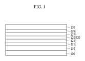
- FIG. 1 is a schematic cross-sectional view showing an organic light emitting diode device according to one embodiment.
- the organic light emitting diode device includes a substrate 100, a first electrode 110 disposed on the substrate, an organic layer 120 disposed on the first electrode 110, and a second electrode 130 disposed on the organic layer 120.
- the substrate 100 may include a substrate commonly used for an organic light emitting diode device, and in particular, a glass substrate, a plastic substrate, and the like may be used.
- the first electrode 110 may be an anode, and may comprise a transparent conductor or an opaque conductor.
- the transparent conductor may include ITO (indium tin oxide), IZO (indium zinc oxide), TO (tin oxide), ZnO (zinc oxide), or a combination thereof.
- the opaque conductor may include silver (Ag), magnesium (Mg), aluminum (Al), platinum (Pt), palladium (Pd), gold (Au), nickel (Ni), neodymium (Nd), iridium (Ir), chromium (Cr), or a combination thereof.
- the first electrode 110 may be a bottom emission type emitting light from the bottom.
- the organic layer 120 may include at least one layer among a hole injection layer 121, a hole transport layer 123, an emission layer 125, an electron transport layer 127, and an electron injection layer 129 that are sequentially positioned on the first electrode.
- the organic layer 120 may include a metal complex compound used for forming at least one layer among the hole injection layer 121, the hole transport layer 123, the emission layer 125, the electron transport layer 127, and the electron injection layer 129.
- the metal complex compound may be used to form the emission layer 125 or the electron transport layer 127.
- the second electrode 130 may be a cathode and may be formed of a transparent conductor or an opaque conductor.
- the transparent conductor may include ITO (indium tin oxide), IZO (indium zinc oxide), TO (tin oxide), ZnO (zinc oxide), or a combination thereof.
- the opaque conductor may include silver (Ag), magnesium (Mg), aluminum (Al), platinum (Pt), palladium (Pd), gold (Au), nickel (Ni), neodymium (Nd), iridium (Ir), chromium (Cr), or a combination thereof.
- the second electrode 130 may be a top emission type emitting light from the organic layer 120 to the top.
- the organic layer may comprise the metal complex compound, and may increase luminous efficiency of an organic light emitting diode device and decrease its driving voltage.
- a compound represented by the following Chemical Formula 3-1 was prepared according to the following Reaction Scheme 1-1.
- a compound represented by the following Chemical Formula 3-2 was prepared according to the following Reaction Scheme 1-2.
- a compound represented by the following Chemical Formula 3-3 was prepared according to the following Reaction Scheme 1-3.
- a compound represented by the following Chemical Formula 3-4 was prepared according to the following Reaction Scheme 1-4.
- a compound represented by the following Chemical Formula 3-5 was prepared according to the following Reaction Scheme 1-5.
- a compound represented by the following Chemical Formula 3-6 was prepared according to the following Reaction Scheme 1-6.
- a compound represented by the following Chemical Formula 3-7 was prepared according to the following Reaction Scheme 1-7.
- a compound represented by the following Chemical Formula 3-8 was prepared according to the following Reaction Scheme 1-8.
- a compound represented by the following Chemical Formula 3-9 was prepared according to the following Reaction Scheme 1-9.
- a compound represented by the following Chemical Formula 3-10 was prepared according to the following Reaction Scheme 1-10.
- a compound represented by the following Chemical Formula 3-11 was prepared according to the following Reaction Scheme 1-11.
- a compound represented by the following Chemical Formula 3-12 was prepared according to the following Reaction Scheme 1-12.
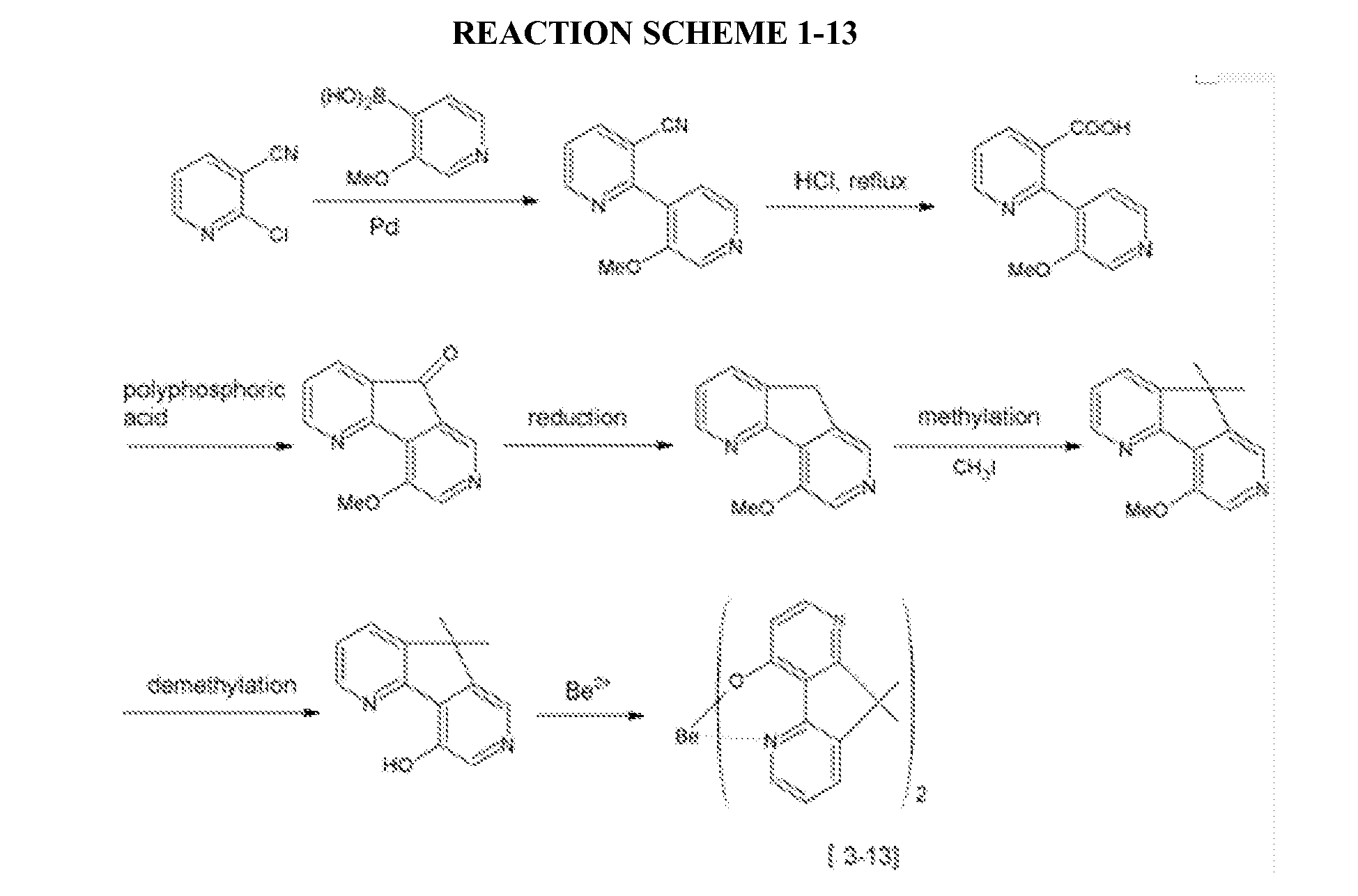
- a compound represented by the following Chemical Formula 3-13 was prepared according to the following Reaction Scheme 1-13.
- a compound represented by the following Chemical Formula 3-14 was prepared according to the following Reaction Scheme 1-14.
- Chemical Formula 4-1 is 4,4'-bis(N-carbazolyl)-1,1'-biphenyl (CBP).
- a compound represented by the following Chemical Formula 4-2 was used, which is aluminum(III)bis(2-methyl-8-quinolinato)4-phenylphenolate (BAlq).
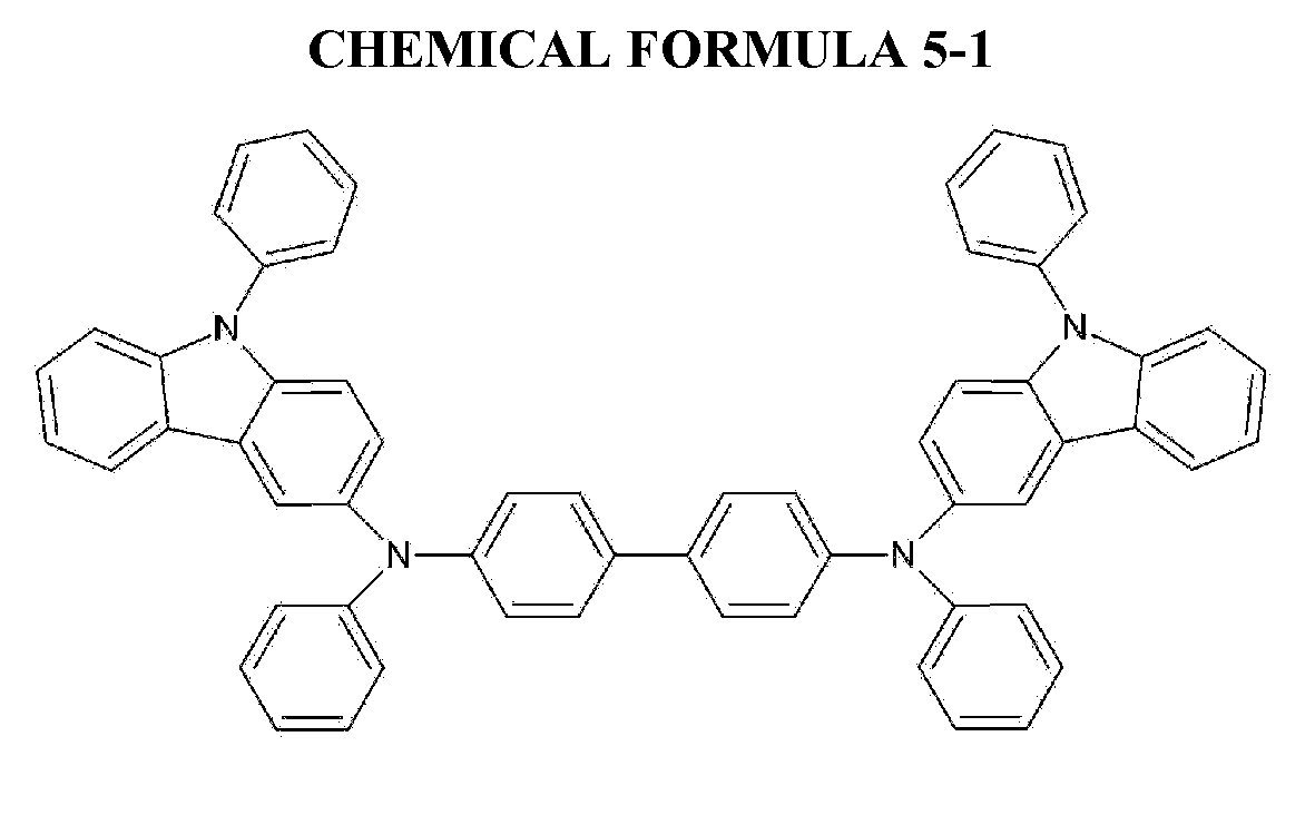
- a lower electrode was prepared by laminating Ag/ITO on a glass substrate and patterning it, and then disposing a hole injection layer to be 70 nm thick on the lower electrode by depositing a compound represented by the following Chemical Formula 5-1, an interlayer to be 5 nm thick thereon by depositing another compound represented by following Chemical Formula 5-2, and a hole transport layer to be 100 nm thick thereon by depositing a compound represented by the following Chemical Formula 5-3.
- a green phosphorescence emission layer was disposed to be 40 nm thick by depositing a compound represented by the following Chemical Formula 5-4 as a dopant and another compound represented by the above Chemical Formula 3-1 prepared in Example 1 as a host.
- an electron transport layer was disposed to be 30 nm thick thereon by depositing a compound represented by the following Chemical Formula 5-5, and an electron injection layer was disposed to be 0.5 nm thick thereon by depositing a compound represented by the following Chemical Formula 5-6.
- an upper electrode was disposed to be 200 nm thick thereon by depositing MgAg, fabricating an organic light emitting diode device.
- the green phosphorescence emission layer included the dopant in an amount of 12 wt% based on the entire amount of the emission layer.
- the electron injection layer was included in an amount of 50 wt% based on the entire amount of the electron transport layer and the electron injection layer.
- An organic light emitting diode device was fabricated according to the same method as Example 2-1, except for using the compound represented by the above Chemical Formula 3-2 prepared according to Example 1-2 as a host.
- An organic light emitting diode device was fabricated according to the same method as Example 2-1, except for using the compound represented by the above Chemical Formula 3-3 prepared according to Example 1-3 as a host.
- An organic light emitting diode device was fabricated according to the same method as Example 2-1, except for using the compound represented by the above Chemical Formula 3-4 prepared according to Example 1-4 as a host.
- An organic light emitting diode device was fabricated according to the same method as Example 2-1, except for using the compound represented by the above Chemical Formula 3-5 prepared according to Example 1-5 as a host.
- An organic light emitting diode device was fabricated according to the same method as Example 2-1, except for using the compound represented by the above Chemical Formula 3-6 prepared according to Example 1-6 as a host.
- An organic light emitting diode device was fabricated according to the same method as Example 2-1, except for using the compound represented by the above Chemical Formula 3-7 prepared according to Example 1-7 as a host.
- An organic light emitting diode device was fabricated according to the same method as Example 2-1, except for using the compound represented by the above Chemical Formula 3-8 prepared according to Example 1-8 as a host.
- An organic light emitting diode device was fabricated according to the same method as Example 2-1, except for using the compound represented by the above Chemical Formula 3-9 prepared according to Example 1-9 as a host.
- An organic light emitting diode device was fabricated according to the same method as Example 2-1, except for using the compound represented by the above Chemical Formula 3-10 prepared according to Example 1-10 as a host.
- An organic light emitting diode device was fabricated according to the same method as Example 2-1, except for using the compound represented by the above Chemical Formula 3-11 1 prepared according to Example 1-11 as a host.
- An organic light emitting diode device was fabricated according to the same method as Example 2-1, except for using the compound represented by the above Chemical Formula 3-12 prepared according to Example 1-12 as a host.
- An organic light emitting diode device was fabricated according to the same method as Example 2-1, except for using the compound represented by the above Chemical Formula 3-13 3 prepared according to Example 1-13 as a host.
- An organic light emitting diode device was fabricated according to the same method as Example 2-1, except for using the compound represented by the above Chemical Formula 3-14 prepared according to Example 1-14 as a host.
- An organic light emitting diode device was fabricated according to the same method as Example 2-1, except for using the compound represented by the above Chemical Formula 4-1 prepared according to Comparative Example 1-1 as a host.
- a lower electrode was prepared by laminating Ag/ITO on a glass substrate and patterning it, and then disposing a hole injection layer be 70 nm thick thereon by depositing a compound represented by the above Chemical Formula 5-1 to, an interlayer to be 5 nm thick thereon by depositing a compound represented by the above Chemical Formula 5-2, and a hole transport layer to be 155 nm thick thereon by depositing a compound represented by the above Chemical Formula 5-3.
- a red phosphorescence emission layer including a compound represented by the following Chemical Formula 5-7 as a dopant and a compound represented by the above Chemical Formula 3-1 prepared according to Example 1-1 as a host was formed to be 40 nm thick thereon.
- an electron transport layer was disposed to be 30 nm thick thereon by depositing a compound represented by the above Chemical Formula 5-5, and an electron injection layer was disposed to be 0.5 nm thick thereon by depositing a compound represented by the above Chemical Formula 5-6.
- an upper electrode was disposed by depositing MgAg to be 200 nm thick, fabricating an organic light emitting diode device.
- the red phosphorescence emission layer included the dopant in an amount of 10 wt% based on the entire weight of the emission layer.
- the electron injection layer was included in an amount of 50 wt% based on the entire weight of the electron transport layer and the electron injection layer.
- An organic light emitting diode device was fabricated according to the same method as Example 3-1, except for using a compound represented by the above Chemical Formula 3-2 prepared according to Example 1-2 as a host.
- An organic light emitting diode device was fabricated according to the same method as Example 3-1, except for using a compound represented by the above Chemical Formula 3-3 prepared according to Example 1-3 as a host.
- An organic light emitting diode device was fabricated according to the same method as Example 3-1, except for using a compound represented by the above Chemical Formula 3-4 prepared according to Example 1-4 as a host.
- An organic light emitting diode device was fabricated according to the same method as Example 3-1, except for using a compound represented by the above Chemical Formula 3-5 prepared according to Example 1-5 as a host.
- An organic light emitting diode device was fabricated according to the same method as Example 3-1, except for using a compound represented by the above Chemical Formula 3-6 prepared according to Example 1-6 as a host.
- An organic light emitting diode device was fabricated according to the same method as Example 3-1, except for using a compound represented by the above Chemical Formula 3-7 prepared according to Example 1-7 as a host.
- An organic light emitting diode device was fabricated according to the same method as Example 3-1, except for using a compound represented by the above Chemical Formula 3-8 prepared according to Example 1-8 as a host.
- An organic light emitting diode device was fabricated according to the same method as Example 3-1, except for using a compound represented by the above Chemical Formula 3-9 prepared according to Example 1-9 as a host.
- An organic light emitting diode device was fabricated according to the same method as Example 3-1, except for using a compound represented by the above Chemical Formula 3-10 prepared according to Example 1-10 as a host.
- An organic light emitting diode device was fabricated according to the same method as Example 3-1, except for using a compound represented by the above Chemical Formula 3-11 1 prepared according to Example 1-11 as a host.
- An organic light emitting diode device was fabricated according to the same method as Example 3-1, except for using a compound represented by the above Chemical Formula 3-12 prepared according to Example 1-12 as a host.
- An organic light emitting diode device was fabricated according to the same method as Example 3-13, except for using a compound represented by the above Chemical Formula 3-2 prepared according to Example 1-13 as a host.
- An organic light emitting diode device was fabricated according to the same method as Example 3-1, except for using a compound represented by the above Chemical Formula 3-14 prepared according to Example 1-14 as a host.
- An organic light emitting diode device was fabricated according to the same method as Example 3-1, except for using a compound represented by the above Chemical Formula 4-2 prepared according to Comparative Example 1-2.
- the organic light emitting diode devices according to Examples 2-1 to 2-14 had higher efficiency and similar color coordinates to the one according to Comparative Example 2.
- the organic light emitting diode devices according to Examples 3-1 to 3-14 had higher efficiency and similar color coordinates to the one of Comparative Example 3.
Landscapes
- Chemical & Material Sciences (AREA)
- Organic Chemistry (AREA)
- Materials Engineering (AREA)
- Engineering & Computer Science (AREA)
- Inorganic Chemistry (AREA)
- Physics & Mathematics (AREA)
- Spectroscopy & Molecular Physics (AREA)
- Crystallography & Structural Chemistry (AREA)
- Optics & Photonics (AREA)
- Electroluminescent Light Sources (AREA)
- Other In-Based Heterocyclic Compounds (AREA)
- Plural Heterocyclic Compounds (AREA)
- Nitrogen Condensed Heterocyclic Rings (AREA)
- Organic Low-Molecular-Weight Compounds And Preparation Thereof (AREA)
Abstract

Description
- This disclosure relates to a metal complex compound and an organic light emitting diode device including the same.
- Recently, an organic light emitting diode (OLED) device has been drawing attention as a display device and a luminous device.
- An organic light emitting diode device includes two electrodes and an emission layer interposed therebetween, and emits light when electrons injected from one electrode are combined with holes injected from another electrode in an emission layer to generate excitons that release energy.
- Since the organic light emitting diode device emits light in itself without a particular light source, it has excellent response speed, viewing angle, and contrast ratio as well as low power consumption.
- An organic light emitting diode device has been required to have increased luminous efficiency but decreased driving voltage.
- One aspect of this disclosure provides a metal complex compound being capable of increasing luminous efficiency and reducing a driving voltage.
- Another aspect of this disclosure provides an organic light emitting diode device including the metal complex compound.
- According to one aspect of this disclosure, provided is a metal complex compound represented by the following Chemical Formula 1.


- In Chemical Formula 1, M is a Group 2 metal ion or Group 3 metal ion, R1 to R8 are the same or different, and are hydrogen, a halogen, a hydroxy group, a substituted or unsubstituted C1 to C20 alkyl group, a substituted or unsubstituted C2 to C20 alkenyl group, a substituted or unsubstituted C2 to C20 alkynyl group, a substituted or unsubstituted C 1 to C20 alkoxy group, a substituted or unsubstituted C3 to C30 cycloalkyl group, a substituted or unsubstituted C3 to C30 cycloalkenyl group, a substituted or unsubstituted C3 to C30 cycloalkynyl group, a substituted or unsubstituted C2 to C30 heterocycloalkyl group, a substituted or unsubstituted C2 to C30 heterocycloalkenyl group, a substituted or unsubstituted C2 to C30 heterocycloalkynyl group, a substituted or unsubstituted C6 to C30 aryl group, a substituted or unsubstituted C6 to C30 aryloxy group, a substituted or unsubstituted C3 to C30 heteroaryl group, an amine group, an ester group, a carboxyl group, a nitro group, or a cyano group, optionally, R1 and R2, R2 and R3, R4 and R5, and R5 and R6 are respectively bound to each other to form a substituted or unsubstituted C6 to C30 aryl group, a substituted or unsubstituted C6 to C30 aryloxy group, or a substituted or unsubstituted C3 to C30 heteroaryl group, A1 to A6 are the same or different, and are a carbon atom or a nitrogen atom, and y is 2 or 3.
- According to another aspect of the present invention, an organic light emitting device is provided, which includes a first electrode, a second electrode facing the first electrode, and an organic layer interposed between the first electrode and the second electrode, wherein the organic layer includes a metal complex compound represented by the above Chemical Formula 1.
- Further aspects of the invention could be learned from the description and claims and are described therein in more detail.
- This disclosure may increase luminous efficiency of an organic light emitting device, while reducing its driving voltage.
-
-
FIG. 1 is the schematic cross-sectional view of an organic light emitting diode device according to one aspect of the present disclosure. - The present invention will be described more fully hereinafter with reference to the accompanying drawings, in which example embodiments of this disclosure are shown.
- In the drawings, the thickness of layers, films, panels, regions, etc., are exaggerated for clarity. Like reference numerals designate like elements throughout the specification. It will be understood that when an element such as a layer, film, region, or substrate is referred to as being "on" another element, it can be directly on the other element or intervening elements may also be present. In contrast, when an element is referred to as being "directly on" another element, there are no intervening elements present.
- As used herein, when a definition is not otherwise provided, the term "substituted" refers to one substituted with a halogen, a hydroxy group, a C1 to C20 alkyl group, a C2 to C20 alkenyl group, a C2 to C20 alkynyl group, a C1 to C20 alkoxy group, a C3 to C30 cycloalkyl group, a C3 to C30 cycloalkenyl group, a C3 to C30 cycloalkynyl group, a C2 to C30 heterocycloalkyl group, a C2 to C30 heterocycloalkenyl group, a C2 to C30 heterocycloalkynyl group, a C6 to C30 aryl group, a C6 to C30 aryloxy group, a C3 to C30 heteroaryl group, an amine group, an ester group, a carboxyl group, a nitro group, or a cyano group, instead of at least one hydrogen atom.
- As used herein, when a definition is not otherwise provided, the term "heterocycloalkyl group", "heterocycloalkenyl group", "heterocycloalkynyl group", and "heteroaryl group" respectively refer to a heterocycloalkyl group, a heterocycloalkenyl group, a heterocycloalkynyl group, and a heteroaryl group including at least one of N, O, S, and P in a cycle of a cycloalkyl group, a cycloalkenyl group, a cycloalkynyl group, and an aryl group.
- The metal complex compound according to the present invention is represented by the following Chemical Formula 1.

- In Chemical Formula 1, M is a Group 2 metal ion or Group 3 metal ion, R1 to R8 are the same or different, and are hydrogen, a halogen, a hydroxy group, a substituted or unsubstituted C1 to C20 alkyl group, a substituted or unsubstituted C2 to C20 alkenyl group, a substituted or unsubstituted C2 to C20 alkynyl group, a substituted or unsubstituted C1 to C20 alkoxy group, a substituted or unsubstituted C3 to C30 cycloalkyl group, a substituted or unsubstituted C3 to C30 cycloalkenyl group, a substituted or unsubstituted C3 to C30 cycloalkynyl group, a substituted or unsubstituted C2 to C30 heterocycloalkyl group, a substituted or unsubstituted C2 to C30 heterocycloalkenyl group, a substituted or unsubstituted C2 to C30 heterocycloalkynyl group, a substituted or unsubstituted C6 to C30 aryl group, a substituted or unsubstituted C6 to C30 aryloxy group, a substituted or unsubstituted C3 to C30 heteroaryl group, an amine group, an ester group, a carboxyl group, a nitro group, or a cyano group, optionally, R1 and R2, R2 and R3, R4 and R5, and R5 and R6 may be respectively bound to each other to form a substituted or unsubstituted C6 to C30 aryl group, a substituted or unsubstituted C6 to C30 aryloxy group, or a substituted or unsubstituted C3 to C30 heteroaryl group, A1 to A6 are the same or different, and are a carbon atom or a nitrogen atom, and y is 2 or 3.
- In Chemical Formula 1, R1 to R8 may be the same or different, and may be hydrogen, a halogen, a substituted or unsubstituted C1 to C20 alkyl group, a substituted or unsubstituted C6 to C30 aryl group, a substituted or unsubstituted C6 to C30 aryloxy group, a substituted or unsubstituted C3 to C30 heteroaryl group, an amine group, an ester group, a nitro group, or a cyano group. Optionally, R1 and R2, R2 and R3, R4 and R5, and R5 and R6 may be respectively bound to each other to form a substituted or unsubstituted C6 to C30 aryl group, a substituted or unsubstituted C6 to C30 aryloxy group, or a substituted or unsubstituted C3 to C30 heteroaryl group.
- In Chemical Formula 1, M may be Be, Zn, Mg, Ca, Y, B, Al, Ga, In, or a combination thereof.
- Examples of the metal complex compound include one of the following Chemical Formulae 2-1 to 2-147.


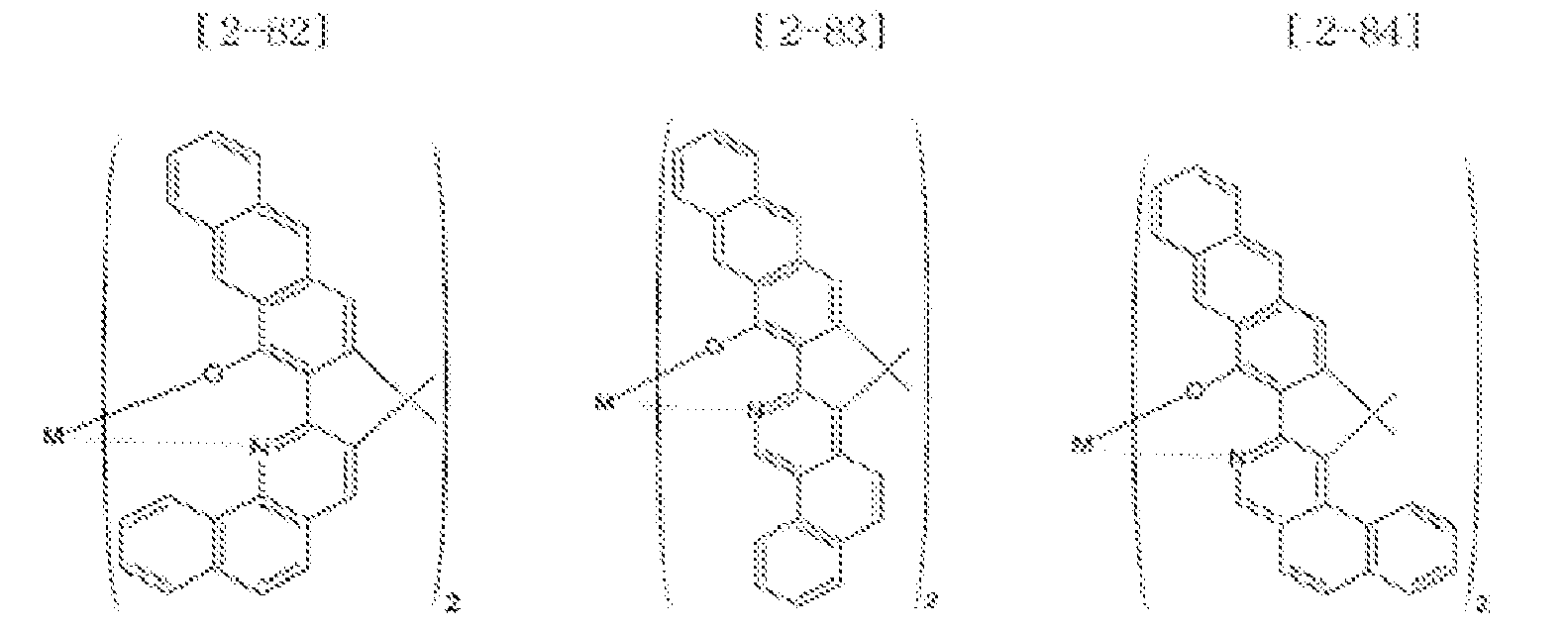


- In Chemical Formulae 2-1 to 2-147, A1 to A18 are the same or different, and are a carbon atom or a nitrogen atom, provided that at least one of A1 to A18 is a nitrogen atom, and M is Be or Zn.
- Referring to
FIG. 1 , an organic light emitting diode device according to one embodiment is described. -
FIG. 1 is a schematic cross-sectional view showing an organic light emitting diode device according to one embodiment. - Referring to
FIG. 1 , the organic light emitting diode device includes asubstrate 100, afirst electrode 110 disposed on the substrate, anorganic layer 120 disposed on thefirst electrode 110, and asecond electrode 130 disposed on theorganic layer 120. - The
substrate 100 may include a substrate commonly used for an organic light emitting diode device, and in particular, a glass substrate, a plastic substrate, and the like may be used. - The
first electrode 110 may be an anode, and may comprise a transparent conductor or an opaque conductor. The transparent conductor may include ITO (indium tin oxide), IZO (indium zinc oxide), TO (tin oxide), ZnO (zinc oxide), or a combination thereof. The opaque conductor may include silver (Ag), magnesium (Mg), aluminum (Al), platinum (Pt), palladium (Pd), gold (Au), nickel (Ni), neodymium (Nd), iridium (Ir), chromium (Cr), or a combination thereof. When thefirst electrode 110 comprises a transparent conductor, it may be a bottom emission type emitting light from the bottom. - The
organic layer 120 may include at least one layer among ahole injection layer 121, ahole transport layer 123, anemission layer 125, anelectron transport layer 127, and anelectron injection layer 129 that are sequentially positioned on the first electrode. - The
organic layer 120 may include a metal complex compound used for forming at least one layer among thehole injection layer 121, thehole transport layer 123, theemission layer 125, theelectron transport layer 127, and theelectron injection layer 129. In particular, the metal complex compound may be used to form theemission layer 125 or theelectron transport layer 127. - The
second electrode 130 may be a cathode and may be formed of a transparent conductor or an opaque conductor. The transparent conductor may include ITO (indium tin oxide), IZO (indium zinc oxide), TO (tin oxide), ZnO (zinc oxide), or a combination thereof. The opaque conductor may include silver (Ag), magnesium (Mg), aluminum (Al), platinum (Pt), palladium (Pd), gold (Au), nickel (Ni), neodymium (Nd), iridium (Ir), chromium (Cr), or a combination thereof. When thesecond electrode 130 comprises a transparent conductor, it may be a top emission type emitting light from theorganic layer 120 to the top. - The organic layer may comprise the metal complex compound, and may increase luminous efficiency of an organic light emitting diode device and decrease its driving voltage.
- The following examples illustrate this disclosure in more detail. These examples, however, are not in any sense to be interpreted as limiting the scope of this disclosure.
- A compound represented by the following Chemical Formula 3-1 was prepared according to the following Reaction Scheme 1-1.

- A compound represented by the following Chemical Formula 3-2 was prepared according to the following Reaction Scheme 1-2.

- A compound represented by the following Chemical Formula 3-3 was prepared according to the following Reaction Scheme 1-3.

- A compound represented by the following Chemical Formula 3-4 was prepared according to the following Reaction Scheme 1-4.

- A compound represented by the following Chemical Formula 3-5 was prepared according to the following Reaction Scheme 1-5.

- A compound represented by the following Chemical Formula 3-6 was prepared according to the following Reaction Scheme 1-6.

- A compound represented by the following Chemical Formula 3-7 was prepared according to the following Reaction Scheme 1-7.

- A compound represented by the following Chemical Formula 3-8 was prepared according to the following Reaction Scheme 1-8.

- A compound represented by the following Chemical Formula 3-9 was prepared according to the following Reaction Scheme 1-9.

- A compound represented by the following Chemical Formula 3-10 was prepared according to the following Reaction Scheme 1-10.

- A compound represented by the following Chemical Formula 3-11 was prepared according to the following Reaction Scheme 1-11.

- A compound represented by the following Chemical Formula 3-12 was prepared according to the following Reaction Scheme 1-12.

- A compound represented by the following Chemical Formula 3-13 was prepared according to the following Reaction Scheme 1-13.
- A compound represented by the following Chemical Formula 3-14 was prepared according to the following Reaction Scheme 1-14.

- A compound represented by the following Chemical Formula 4-1 was used, which is 4,4'-bis(N-carbazolyl)-1,1'-biphenyl (CBP).

- A compound represented by the following Chemical Formula 4-2 was used, which is aluminum(III)bis(2-methyl-8-quinolinato)4-phenylphenolate (BAlq).

- A lower electrode was prepared by laminating Ag/ITO on a glass substrate and patterning it, and then disposing a hole injection layer to be 70 nm thick on the lower electrode by depositing a compound represented by the following Chemical Formula 5-1, an interlayer to be 5 nm thick thereon by depositing another compound represented by following Chemical Formula 5-2, and a hole transport layer to be 100 nm thick thereon by depositing a compound represented by the following Chemical Formula 5-3. Next, a green phosphorescence emission layer was disposed to be 40 nm thick by depositing a compound represented by the following Chemical Formula 5-4 as a dopant and another compound represented by the above Chemical Formula 3-1 prepared in Example 1 as a host. Then, an electron transport layer was disposed to be 30 nm thick thereon by depositing a compound represented by the following Chemical Formula 5-5, and an electron injection layer was disposed to be 0.5 nm thick thereon by depositing a compound represented by the following Chemical Formula 5-6. Next, an upper electrode was disposed to be 200 nm thick thereon by depositing MgAg, fabricating an organic light emitting diode device. Herein, the green phosphorescence emission layer included the dopant in an amount of 12 wt% based on the entire amount of the emission layer. The electron injection layer was included in an amount of 50 wt% based on the entire amount of the electron transport layer and the electron injection layer.


- An organic light emitting diode device was fabricated according to the same method as Example 2-1, except for using the compound represented by the above Chemical Formula 3-2 prepared according to Example 1-2 as a host.
- An organic light emitting diode device was fabricated according to the same method as Example 2-1, except for using the compound represented by the above Chemical Formula 3-3 prepared according to Example 1-3 as a host.
- An organic light emitting diode device was fabricated according to the same method as Example 2-1, except for using the compound represented by the above Chemical Formula 3-4 prepared according to Example 1-4 as a host.
- An organic light emitting diode device was fabricated according to the same method as Example 2-1, except for using the compound represented by the above Chemical Formula 3-5 prepared according to Example 1-5 as a host.
- An organic light emitting diode device was fabricated according to the same method as Example 2-1, except for using the compound represented by the above Chemical Formula 3-6 prepared according to Example 1-6 as a host.
- An organic light emitting diode device was fabricated according to the same method as Example 2-1, except for using the compound represented by the above Chemical Formula 3-7 prepared according to Example 1-7 as a host.
- An organic light emitting diode device was fabricated according to the same method as Example 2-1, except for using the compound represented by the above Chemical Formula 3-8 prepared according to Example 1-8 as a host.
- An organic light emitting diode device was fabricated according to the same method as Example 2-1, except for using the compound represented by the above Chemical Formula 3-9 prepared according to Example 1-9 as a host.
- An organic light emitting diode device was fabricated according to the same method as Example 2-1, except for using the compound represented by the above Chemical Formula 3-10 prepared according to Example 1-10 as a host.
- An organic light emitting diode device was fabricated according to the same method as Example 2-1, except for using the compound represented by the above Chemical Formula 3-11 1 prepared according to Example 1-11 as a host.
- An organic light emitting diode device was fabricated according to the same method as Example 2-1, except for using the compound represented by the above Chemical Formula 3-12 prepared according to Example 1-12 as a host.
- An organic light emitting diode device was fabricated according to the same method as Example 2-1, except for using the compound represented by the above Chemical Formula 3-13 3 prepared according to Example 1-13 as a host.
- An organic light emitting diode device was fabricated according to the same method as Example 2-1, except for using the compound represented by the above Chemical Formula 3-14 prepared according to Example 1-14 as a host.
- An organic light emitting diode device was fabricated according to the same method as Example 2-1, except for using the compound represented by the above Chemical Formula 4-1 prepared according to Comparative Example 1-1 as a host.
- A lower electrode was prepared by laminating Ag/ITO on a glass substrate and patterning it, and then disposing a hole injection layer be 70 nm thick thereon by depositing a compound represented by the above Chemical Formula 5-1 to, an interlayer to be 5 nm thick thereon by depositing a compound represented by the above Chemical Formula 5-2, and a hole transport layer to be 155 nm thick thereon by depositing a compound represented by the above Chemical Formula 5-3. Next, a red phosphorescence emission layer including a compound represented by the following Chemical Formula 5-7 as a dopant and a compound represented by the above Chemical Formula 3-1 prepared according to Example 1-1 as a host was formed to be 40 nm thick thereon. Then, an electron transport layer was disposed to be 30 nm thick thereon by depositing a compound represented by the above Chemical Formula 5-5, and an electron injection layer was disposed to be 0.5 nm thick thereon by depositing a compound represented by the above Chemical Formula 5-6. On the lower electrode, an upper electrode was disposed by depositing MgAg to be 200 nm thick, fabricating an organic light emitting diode device. Herein, the red phosphorescence emission layer included the dopant in an amount of 10 wt% based on the entire weight of the emission layer. The electron injection layer was included in an amount of 50 wt% based on the entire weight of the electron transport layer and the electron injection layer.

- An organic light emitting diode device was fabricated according to the same method as Example 3-1, except for using a compound represented by the above Chemical Formula 3-2 prepared according to Example 1-2 as a host.
- An organic light emitting diode device was fabricated according to the same method as Example 3-1, except for using a compound represented by the above Chemical Formula 3-3 prepared according to Example 1-3 as a host.
- An organic light emitting diode device was fabricated according to the same method as Example 3-1, except for using a compound represented by the above Chemical Formula 3-4 prepared according to Example 1-4 as a host.
- An organic light emitting diode device was fabricated according to the same method as Example 3-1, except for using a compound represented by the above Chemical Formula 3-5 prepared according to Example 1-5 as a host.
- An organic light emitting diode device was fabricated according to the same method as Example 3-1, except for using a compound represented by the above Chemical Formula 3-6 prepared according to Example 1-6 as a host.
- An organic light emitting diode device was fabricated according to the same method as Example 3-1, except for using a compound represented by the above Chemical Formula 3-7 prepared according to Example 1-7 as a host.
- An organic light emitting diode device was fabricated according to the same method as Example 3-1, except for using a compound represented by the above Chemical Formula 3-8 prepared according to Example 1-8 as a host.
- An organic light emitting diode device was fabricated according to the same method as Example 3-1, except for using a compound represented by the above Chemical Formula 3-9 prepared according to Example 1-9 as a host.
- An organic light emitting diode device was fabricated according to the same method as Example 3-1, except for using a compound represented by the above Chemical Formula 3-10 prepared according to Example 1-10 as a host.
- An organic light emitting diode device was fabricated according to the same method as Example 3-1, except for using a compound represented by the above Chemical Formula 3-11 1 prepared according to Example 1-11 as a host.
- An organic light emitting diode device was fabricated according to the same method as Example 3-1, except for using a compound represented by the above Chemical Formula 3-12 prepared according to Example 1-12 as a host.
- An organic light emitting diode device was fabricated according to the same method as Example 3-13, except for using a compound represented by the above Chemical Formula 3-2 prepared according to Example 1-13 as a host.
- An organic light emitting diode device was fabricated according to the same method as Example 3-1, except for using a compound represented by the above Chemical Formula 3-14 prepared according to Example 1-14 as a host.
- An organic light emitting diode device was fabricated according to the same method as Example 3-1, except for using a compound represented by the above Chemical Formula 4-2 prepared according to Comparative Example 1-2.
- The organic light emitting diode devices according to Examples 2-1 to 2-14 and Comparative Example 2 were evaluated regarding luminous efficiency and color characteristic. The results are provided in the following Table 1.
TABLE 1 Voltage (V) Efficiency (cd/A) Color coordinates (CIE) Maximum emission wavelength (A max) (nm) x y Example 2-1 5.3 42 0.330 0.612 518 Example 2-2 4.8 39 0.327 0.611 517 Example 2-3 4.8 38 0.328 0.613 517 Example 2-4 5.0 35 0.325 0.615 516 Example 2-5 5.1 35 0.326 0.614 516 Example 2-6 5.3 41 0.328 0.611 517 Example 2-7 5.4 40 0.331 0.613 518 Example 2-8 5.3 39 0.330 0.613 518 Example 2-9 5.8 34 0.329 0.613 517 Example 2-10 5.1 37 0.329 0.612 517 Example 2-11 4.8 40 0.327 0.611 517 Example 2-12 5.3 35 0.326 0.615 516 Example 2-13 5.3 36 0.330 0.613 518 Example 2-14 5.0 34 0.326 0.615 516 Comparative Example 2 6.1 33 0.327 0.611 517 - Referring to Table 1, the organic light emitting diode devices according to Examples 2-1 to 2-14 had higher efficiency and similar color coordinates to the one according to Comparative Example 2.
- The organic light emitting diode devices according to Examples 3-1 to 3-14 and Comparative Example 3 were evaluated regarding luminous efficiency and color characteristic. The results are provided in the following Table 2.
TABLE 2 Voltage (V) Efficiency (cd/A) Color coordinates (CIE) Maximum emission wavelength (λ max) (nm) x y Example 3-1 5.4 20 0.661 0.338 625 Example 3-2 4.7 23 0.663 0.337 626 Example 3-3 4.7 24 0.662 0.338 625 Example 3-4 4.2 29 0.660 0.340 624 Example 3-5 4.3 30 0.661 0.339 625 Example 3-6 4.8 23 0.661 0.338 625 Example 3-7 4.9 22 0.660 0.340 625 Example 3-8 5.1 21 0.662 0.338 626 Example 3-9 4.7 26 0.660 0.340 625 Example 3-10 4.9 25 0.662 0.337 625 Example 3-11 4.6 27 0.660 0.340 624 Example 3-12 5.1 23 0.662 0.338 625 Example 3-13 5.3 21 0.661 0.339 625 Example 3-14 4.9 24 0.660 0.340 625 Comparative Example 3 5.6 19 0.661 0.338 625 - Referring to Table 2, the organic light emitting diode devices according to Examples 3-1 to 3-14 had higher efficiency and similar color coordinates to the one of Comparative Example 3.
Claims (8)
- A metal complex compound of the following Chemical Formula 1:
 M is a Group 2 metal ion or Group 3 metal ion,R1 to R8 are the same or different, and are hydrogen, a halogen, a hydroxy group, a substituted or unsubstituted C1 to C20 alkyl group, a substituted or unsubstituted C2 to C20 alkenyl group, a substituted or unsubstituted C2 to C20 alkynyl group, a substituted or unsubstituted C1 to C20 alkoxy group, a substituted or unsubstituted C3 to C30 cycloalkyl group, a substituted or unsubstituted C3 to C30 cycloalkenyl group, a substituted or unsubstituted C3 to C30 cycloalkynyl group, a substituted or unsubstituted C2 to C30 heterocycloalkyl group, a substituted or unsubstituted C2 to C30 heterocycloalkenyl group, a substituted or unsubstituted C2 to C30 heterocycloalkynyl group, a substituted or unsubstituted C6 to C30 aryl group, a substituted or unsubstituted C6 to C30 aryloxy group, a substituted or unsubstituted C3 to C30 heteroaryl group, an amine group, an ester group, a carboxyl group, a nitro group, or a cyano group,optionally, R1 and R2, R2 and R3, R4 and R5, and R5 and R6 are respectively bound to each other to form a substituted or unsubstituted C6 to C30 aryl group, a substituted or unsubstituted C6 to C30 aryloxy group, or a substituted or unsubstituted C3 to C30 heteroaryl group,A1 to A6 are the same or different, and are a carbon atom or a nitrogen atom, andy is 2 or 3.
 - The metal complex compound of claim 1, wherein in Chemical Formula 1, R1 to R8 are the same or different, and are hydrogen, a halogen, a substituted or unsubstituted C1 to C20 alkyl group, a substituted or unsubstituted C6 to C30 aryl group, a substituted or unsubstituted C6 to C30 aryloxy group, a substituted or unsubstituted C3 to C30 heteroaryl group, an amine group, an ester group, a nitro group, or a cyano group, and
optionally, R1 and R2, R2 and R3, R4 and R5, and R5 and R6 are respectively bound to each other to form a substituted or unsubstituted C6 to C30 aryl group, a substituted or unsubstituted C6 to C30 aryloxy group, or a substituted or unsubstituted C3 to C30 heteroaryl group. - The metal complex compound of claim 1 or 2, wherein in Chemical Formula 1, M is Be, Zn, Mg, Ca, Y, B, Al, Ga, In, or a combination thereof.
- The metal complex compound of claim 1, wherein the metal complex compound comprises one of the compounds represented by the following Chemical Formulae 2-1 to 2-147:


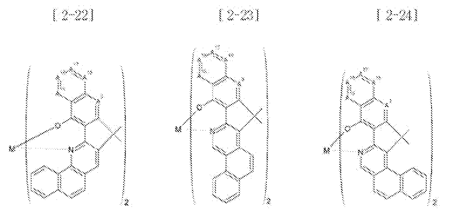


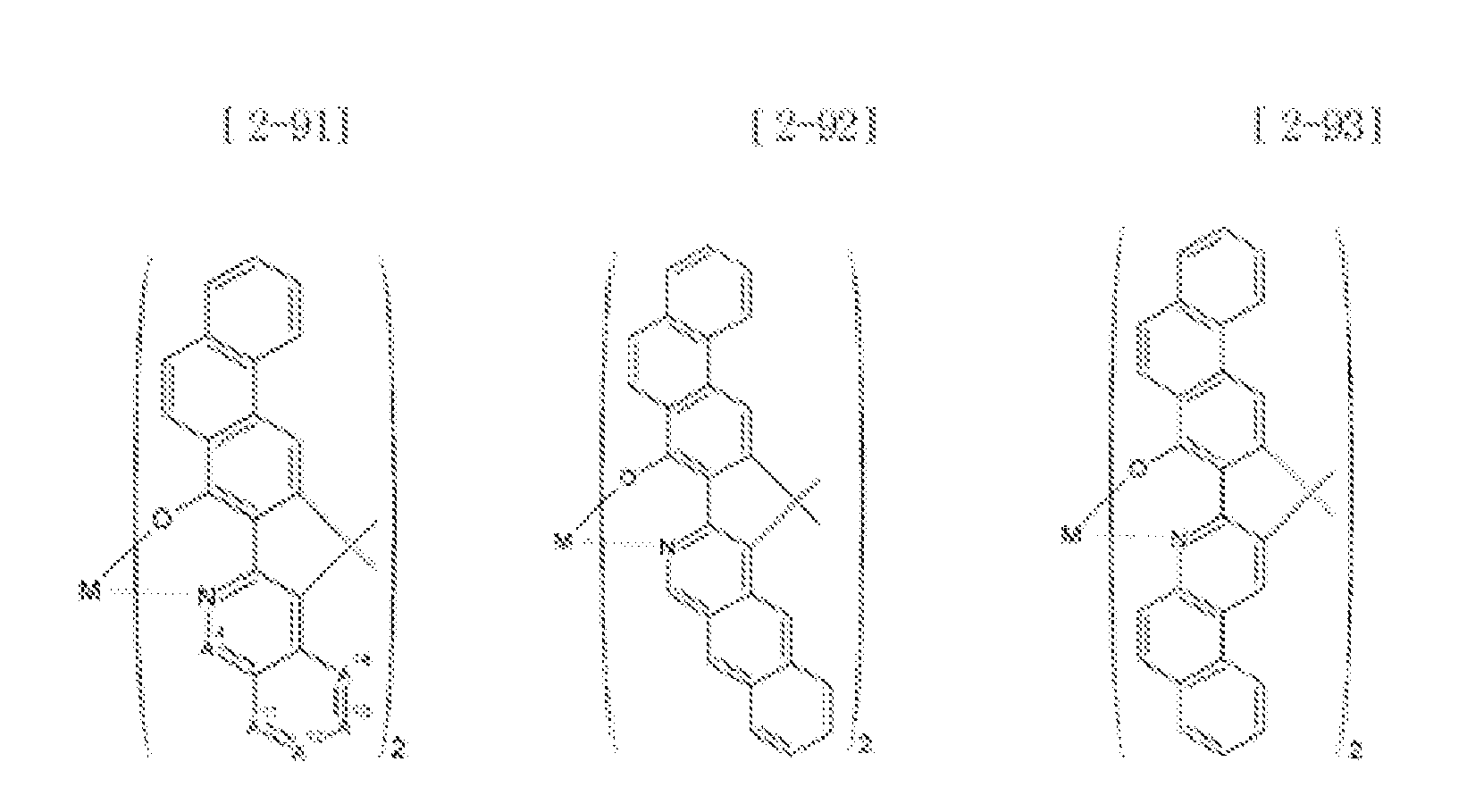


 wherein, in Chemical Formulae 2-1 to 2-147,A1 to A18 are the same or different, and are a carbon atom or a nitrogen atom, provided that at least one of A1 to A18 is a nitrogen atom, andM is Be or Zn.
 - An organic light emitting diode device, comprising:a first electrode;a second electrode facing the first electrode; andan organic layer interposed between the first electrode and the second electrode,wherein the organic layer comprises a metal complex compound of any of claims 1 through 4.
- The organic light emitting diode device of claim 5, wherein the organic layer comprises at least one of a hole injection layer, a hole transport layer, an emission layer, an electron transport layer, and an electron injection layer that are sequentially positioned on the first electrode.
- The organic light emitting diode device of claim 6, wherein the metal complex compound is included in the emission layer.
- The organic light emitting diode device of claim 6, wherein the metal complex compound is included in the electron transport layer.
Applications Claiming Priority (1)
| Application Number | Priority Date | Filing Date | Title |
|---|---|---|---|
| KR1020100068017A KR101201721B1 (en) | 2010-07-14 | 2010-07-14 | Metal complex compound and organic light emitting diode device including the same |
Publications (2)
| Publication Number | Publication Date |
|---|---|
| EP2407458A1 true EP2407458A1 (en) | 2012-01-18 |
| EP2407458B1 EP2407458B1 (en) | 2014-10-29 |
Family
ID=44720229
Family Applications (1)
| Application Number | Title | Priority Date | Filing Date |
|---|---|---|---|
| EP11172555.2A Not-in-force EP2407458B1 (en) | 2010-07-14 | 2011-07-04 | Metal complex compound and organic light emitting diode device including the same |
Country Status (4)
| Country | Link |
|---|---|
| US (2) | US9096529B2 (en) |
| EP (1) | EP2407458B1 (en) |
| JP (1) | JP5850613B2 (en) |
| KR (1) | KR101201721B1 (en) |
Cited By (1)
| Publication number | Priority date | Publication date | Assignee | Title |
|---|---|---|---|---|
| CN109476608A (en) * | 2016-07-11 | 2019-03-15 | 喜星素材株式会社 | Heterocyclic compound and organic light-emitting device using the same |
Families Citing this family (5)
| Publication number | Priority date | Publication date | Assignee | Title |
|---|---|---|---|---|
| KR102021273B1 (en) * | 2011-05-27 | 2019-09-16 | 가부시키가이샤 한도오따이 에네루기 켄큐쇼 | Carbazole compound, light-emitting element, light-emitting device, electronic device, and lighting device |
| KR101512014B1 (en) | 2012-04-05 | 2015-04-16 | (주)씨에스엘쏠라 | New arylcarbazolylacridine-based organic electroluminescent compounds and organic electroluminescent device comprising the same |
| KR20140071897A (en) | 2012-11-26 | 2014-06-12 | 가부시키가이샤 한도오따이 에네루기 켄큐쇼 | Light-emitting element, light-emitting device, electronic device, and lighting device |
| KR102379123B1 (en) | 2015-08-27 | 2022-03-24 | 엘지디스플레이 주식회사 | Organic light emitting display device and lighting apparatus for vehicles using the same |
| US10811618B2 (en) | 2016-12-19 | 2020-10-20 | Universal Display Corporation | Organic electroluminescent materials and devices |
Citations (2)
| Publication number | Priority date | Publication date | Assignee | Title |
|---|---|---|---|---|
| JP2000357588A (en) * | 1999-06-11 | 2000-12-26 | Toyota Central Res & Dev Lab Inc | Organic electroluminescent device |
| US20050019605A1 (en) * | 2003-07-25 | 2005-01-27 | Raymond Kwong | Materials and structures for enhancing the performance of organic light emitting devices |
Family Cites Families (6)
| Publication number | Priority date | Publication date | Assignee | Title |
|---|---|---|---|---|
| JPH07197021A (en) | 1994-01-06 | 1995-08-01 | Fuji Electric Co Ltd | Organic thin film light emitting device |
| JP3475620B2 (en) * | 1995-12-25 | 2003-12-08 | 東洋インキ製造株式会社 | Organic electroluminescent device material and organic electroluminescent device using the same |
| JP2000012222A (en) | 1998-06-19 | 2000-01-14 | Toray Ind Inc | Light emitting element |
| JP2000100569A (en) | 1998-09-22 | 2000-04-07 | Toray Ind Inc | Light emitting element |
| JP4269382B2 (en) * | 1999-01-13 | 2009-05-27 | コニカミノルタホールディングス株式会社 | Organic electroluminescence device |
| DE10345572A1 (en) * | 2003-09-29 | 2005-05-19 | Covion Organic Semiconductors Gmbh | metal complexes |
-
2010
- 2010-07-14 KR KR1020100068017A patent/KR101201721B1/en active Active
- 2010-12-16 JP JP2010280380A patent/JP5850613B2/en active Active
-
2011
- 2011-06-24 US US13/168,760 patent/US9096529B2/en active Active
- 2011-07-04 EP EP11172555.2A patent/EP2407458B1/en not_active Not-in-force
-
2015
- 2015-07-30 US US14/814,085 patent/US20150340628A1/en not_active Abandoned
Patent Citations (2)
| Publication number | Priority date | Publication date | Assignee | Title |
|---|---|---|---|---|
| JP2000357588A (en) * | 1999-06-11 | 2000-12-26 | Toyota Central Res & Dev Lab Inc | Organic electroluminescent device |
| US20050019605A1 (en) * | 2003-07-25 | 2005-01-27 | Raymond Kwong | Materials and structures for enhancing the performance of organic light emitting devices |
Cited By (2)
| Publication number | Priority date | Publication date | Assignee | Title |
|---|---|---|---|---|
| CN109476608A (en) * | 2016-07-11 | 2019-03-15 | 喜星素材株式会社 | Heterocyclic compound and organic light-emitting device using the same |
| CN109476608B (en) * | 2016-07-11 | 2022-09-20 | Lt素材株式会社 | Heterocyclic compound and organic light-emitting device using the same |
Also Published As
| Publication number | Publication date |
|---|---|
| JP2012020986A (en) | 2012-02-02 |
| US20150340628A1 (en) | 2015-11-26 |
| KR20120007312A (en) | 2012-01-20 |
| JP5850613B2 (en) | 2016-02-03 |
| US20120012824A1 (en) | 2012-01-19 |
| EP2407458B1 (en) | 2014-10-29 |
| US9096529B2 (en) | 2015-08-04 |
| KR101201721B1 (en) | 2012-11-15 |
Similar Documents
| Publication | Publication Date | Title |
|---|---|---|
| US20230108554A1 (en) | Deep homo (highest occupied molecular orbital) emitter device structures | |
| US12108668B2 (en) | Host materials for electroluminescent devices | |
| KR101983229B1 (en) | Organic light emitting device and method for manufacturing the same | |
| JP5024124B2 (en) | Organic electroluminescence device and display device | |
| CN103664748B (en) | Pyrene compound and the organic light-emitting diode equipment that comprises this compound | |
| KR20230113709A (en) | Organic Light Emitting Diode Device | |
| US20160276414A1 (en) | One-way transparent display | |
| EP2407458A1 (en) | Metal complex compound and organic light emitting diode device including the same | |
| EP2333865B1 (en) | Organic light emitting diode device | |
| KR20130014470A (en) | Organic electroluminescent device | |
| US20220020945A1 (en) | Color stable organic light emitting diode stack | |
| EP2404976B1 (en) | Organic material and organic light emitting device including the same | |
| KR101481822B1 (en) | Organic light emitting diode and organic electro-luminesence display device | |
| EP3018724B1 (en) | Organic light-emitting device and manufacturing method therefor | |
| KR20220038911A (en) | An organic light emitting diode employing a multi-refractive capping layer for improving a light efficiency | |
| CN105622618A (en) | Organic light emitting display device | |
| JP2881212B2 (en) | EL device | |
| KR102081118B1 (en) | Organic light emitting display | |
| TWI538560B (en) | Organic electroluminescence element | |
| KR20120031771A (en) | Metal complex compound and organic light emitting diode device including the same | |
| JP4770699B2 (en) | Display element | |
| KR102609088B1 (en) | Organic Light Emitting Diode Device | |
| US8835022B2 (en) | Metal complex compound and organic light emitting diode device including the same | |
| KR20130135185A (en) | Organic light emitting device and method for preparing the same | |
| KR102228323B1 (en) | Compound and organic light emitting device comprising the same |
Legal Events
| Date | Code | Title | Description |
|---|---|---|---|
| AK | Designated contracting states |
Kind code of ref document: A1 Designated state(s): AL AT BE BG CH CY CZ DE DK EE ES FI FR GB GR HR HU IE IS IT LI LT LU LV MC MK MT NL NO PL PT RO RS SE SI SK SM TR |
|
| AX | Request for extension of the european patent |
Extension state: BA ME |
|
| PUAI | Public reference made under article 153(3) epc to a published international application that has entered the european phase |
Free format text: ORIGINAL CODE: 0009012 |
|
| 17P | Request for examination filed |
Effective date: 20120703 |
|
| RAP1 | Party data changed (applicant data changed or rights of an application transferred) |
Owner name: SAMSUNG DISPLAY CO., LTD. |
|
| 17Q | First examination report despatched |
Effective date: 20130408 |
|
| GRAP | Despatch of communication of intention to grant a patent |
Free format text: ORIGINAL CODE: EPIDOSNIGR1 |
|
| INTG | Intention to grant announced |
Effective date: 20140617 |
|
| RIN1 | Information on inventor provided before grant (corrected) |
Inventor name: LEE, KWAN-HEE Inventor name: HAMADA, YUJI |
|
| GRAS | Grant fee paid |
Free format text: ORIGINAL CODE: EPIDOSNIGR3 |
|
| GRAA | (expected) grant |
Free format text: ORIGINAL CODE: 0009210 |
|
| AK | Designated contracting states |
Kind code of ref document: B1 Designated state(s): AL AT BE BG CH CY CZ DE DK EE ES FI FR GB GR HR HU IE IS IT LI LT LU LV MC MK MT NL NO PL PT RO RS SE SI SK SM TR |
|
| REG | Reference to a national code |
Ref country code: GB Ref legal event code: FG4D |
|
| REG | Reference to a national code |
Ref country code: CH Ref legal event code: EP |
|
| REG | Reference to a national code |
Ref country code: AT Ref legal event code: REF Ref document number: 693507 Country of ref document: AT Kind code of ref document: T Effective date: 20141115 |
|
| REG | Reference to a national code |
Ref country code: IE Ref legal event code: FG4D |
|
| REG | Reference to a national code |
Ref country code: DE Ref legal event code: R096 Ref document number: 602011010894 Country of ref document: DE Effective date: 20141211 |
|
| REG | Reference to a national code |
Ref country code: AT Ref legal event code: MK05 Ref document number: 693507 Country of ref document: AT Kind code of ref document: T Effective date: 20141029 |
|
| REG | Reference to a national code |
Ref country code: NL Ref legal event code: VDEP Effective date: 20141029 |
|
| REG | Reference to a national code |
Ref country code: LT Ref legal event code: MG4D |
|
| PG25 | Lapsed in a contracting state [announced via postgrant information from national office to epo] |
Ref country code: PT Free format text: LAPSE BECAUSE OF FAILURE TO SUBMIT A TRANSLATION OF THE DESCRIPTION OR TO PAY THE FEE WITHIN THE PRESCRIBED TIME-LIMIT Effective date: 20150302 Ref country code: NO Free format text: LAPSE BECAUSE OF FAILURE TO SUBMIT A TRANSLATION OF THE DESCRIPTION OR TO PAY THE FEE WITHIN THE PRESCRIBED TIME-LIMIT Effective date: 20150129 Ref country code: ES Free format text: LAPSE BECAUSE OF FAILURE TO SUBMIT A TRANSLATION OF THE DESCRIPTION OR TO PAY THE FEE WITHIN THE PRESCRIBED TIME-LIMIT Effective date: 20141029 Ref country code: LT Free format text: LAPSE BECAUSE OF FAILURE TO SUBMIT A TRANSLATION OF THE DESCRIPTION OR TO PAY THE FEE WITHIN THE PRESCRIBED TIME-LIMIT Effective date: 20141029 Ref country code: IS Free format text: LAPSE BECAUSE OF FAILURE TO SUBMIT A TRANSLATION OF THE DESCRIPTION OR TO PAY THE FEE WITHIN THE PRESCRIBED TIME-LIMIT Effective date: 20150228 Ref country code: NL Free format text: LAPSE BECAUSE OF FAILURE TO SUBMIT A TRANSLATION OF THE DESCRIPTION OR TO PAY THE FEE WITHIN THE PRESCRIBED TIME-LIMIT Effective date: 20141029 Ref country code: FI Free format text: LAPSE BECAUSE OF FAILURE TO SUBMIT A TRANSLATION OF THE DESCRIPTION OR TO PAY THE FEE WITHIN THE PRESCRIBED TIME-LIMIT Effective date: 20141029 |
|
| PG25 | Lapsed in a contracting state [announced via postgrant information from national office to epo] |
Ref country code: LV Free format text: LAPSE BECAUSE OF FAILURE TO SUBMIT A TRANSLATION OF THE DESCRIPTION OR TO PAY THE FEE WITHIN THE PRESCRIBED TIME-LIMIT Effective date: 20141029 Ref country code: RS Free format text: LAPSE BECAUSE OF FAILURE TO SUBMIT A TRANSLATION OF THE DESCRIPTION OR TO PAY THE FEE WITHIN THE PRESCRIBED TIME-LIMIT Effective date: 20141029 Ref country code: SE Free format text: LAPSE BECAUSE OF FAILURE TO SUBMIT A TRANSLATION OF THE DESCRIPTION OR TO PAY THE FEE WITHIN THE PRESCRIBED TIME-LIMIT Effective date: 20141029 Ref country code: GR Free format text: LAPSE BECAUSE OF FAILURE TO SUBMIT A TRANSLATION OF THE DESCRIPTION OR TO PAY THE FEE WITHIN THE PRESCRIBED TIME-LIMIT Effective date: 20150130 Ref country code: CY Free format text: LAPSE BECAUSE OF FAILURE TO SUBMIT A TRANSLATION OF THE DESCRIPTION OR TO PAY THE FEE WITHIN THE PRESCRIBED TIME-LIMIT Effective date: 20141029 Ref country code: PL Free format text: LAPSE BECAUSE OF FAILURE TO SUBMIT A TRANSLATION OF THE DESCRIPTION OR TO PAY THE FEE WITHIN THE PRESCRIBED TIME-LIMIT Effective date: 20141029 Ref country code: HR Free format text: LAPSE BECAUSE OF FAILURE TO SUBMIT A TRANSLATION OF THE DESCRIPTION OR TO PAY THE FEE WITHIN THE PRESCRIBED TIME-LIMIT Effective date: 20141029 Ref country code: AT Free format text: LAPSE BECAUSE OF FAILURE TO SUBMIT A TRANSLATION OF THE DESCRIPTION OR TO PAY THE FEE WITHIN THE PRESCRIBED TIME-LIMIT Effective date: 20141029 |
|
| REG | Reference to a national code |
Ref country code: DE Ref legal event code: R097 Ref document number: 602011010894 Country of ref document: DE |
|
| PG25 | Lapsed in a contracting state [announced via postgrant information from national office to epo] |
Ref country code: DK Free format text: LAPSE BECAUSE OF FAILURE TO SUBMIT A TRANSLATION OF THE DESCRIPTION OR TO PAY THE FEE WITHIN THE PRESCRIBED TIME-LIMIT Effective date: 20141029 Ref country code: CZ Free format text: LAPSE BECAUSE OF FAILURE TO SUBMIT A TRANSLATION OF THE DESCRIPTION OR TO PAY THE FEE WITHIN THE PRESCRIBED TIME-LIMIT Effective date: 20141029 Ref country code: EE Free format text: LAPSE BECAUSE OF FAILURE TO SUBMIT A TRANSLATION OF THE DESCRIPTION OR TO PAY THE FEE WITHIN THE PRESCRIBED TIME-LIMIT Effective date: 20141029 Ref country code: RO Free format text: LAPSE BECAUSE OF FAILURE TO SUBMIT A TRANSLATION OF THE DESCRIPTION OR TO PAY THE FEE WITHIN THE PRESCRIBED TIME-LIMIT Effective date: 20141029 Ref country code: SK Free format text: LAPSE BECAUSE OF FAILURE TO SUBMIT A TRANSLATION OF THE DESCRIPTION OR TO PAY THE FEE WITHIN THE PRESCRIBED TIME-LIMIT Effective date: 20141029 |
|
| PG25 | Lapsed in a contracting state [announced via postgrant information from national office to epo] |
Ref country code: IT Free format text: LAPSE BECAUSE OF FAILURE TO SUBMIT A TRANSLATION OF THE DESCRIPTION OR TO PAY THE FEE WITHIN THE PRESCRIBED TIME-LIMIT Effective date: 20141029 |
|
| PLBE | No opposition filed within time limit |
Free format text: ORIGINAL CODE: 0009261 |
|
| STAA | Information on the status of an ep patent application or granted ep patent |
Free format text: STATUS: NO OPPOSITION FILED WITHIN TIME LIMIT |
|
| RAP2 | Party data changed (patent owner data changed or rights of a patent transferred) |
Owner name: SAMSUNG DISPLAY CO., LTD. |
|
| 26N | No opposition filed |
Effective date: 20150730 |
|
| PG25 | Lapsed in a contracting state [announced via postgrant information from national office to epo] |
Ref country code: SI Free format text: LAPSE BECAUSE OF FAILURE TO SUBMIT A TRANSLATION OF THE DESCRIPTION OR TO PAY THE FEE WITHIN THE PRESCRIBED TIME-LIMIT Effective date: 20141029 Ref country code: MC Free format text: LAPSE BECAUSE OF FAILURE TO SUBMIT A TRANSLATION OF THE DESCRIPTION OR TO PAY THE FEE WITHIN THE PRESCRIBED TIME-LIMIT Effective date: 20141029 |
|
| REG | Reference to a national code |
Ref country code: CH Ref legal event code: PL |
|
| PG25 | Lapsed in a contracting state [announced via postgrant information from national office to epo] |
Ref country code: LU Free format text: LAPSE BECAUSE OF FAILURE TO SUBMIT A TRANSLATION OF THE DESCRIPTION OR TO PAY THE FEE WITHIN THE PRESCRIBED TIME-LIMIT Effective date: 20150704 |
|
| REG | Reference to a national code |
Ref country code: IE Ref legal event code: MM4A |
|
| PG25 | Lapsed in a contracting state [announced via postgrant information from national office to epo] |
Ref country code: LI Free format text: LAPSE BECAUSE OF NON-PAYMENT OF DUE FEES Effective date: 20150731 Ref country code: CH Free format text: LAPSE BECAUSE OF NON-PAYMENT OF DUE FEES Effective date: 20150731 |
|
| REG | Reference to a national code |
Ref country code: FR Ref legal event code: PLFP Year of fee payment: 6 |
|
| PG25 | Lapsed in a contracting state [announced via postgrant information from national office to epo] |
Ref country code: IE Free format text: LAPSE BECAUSE OF NON-PAYMENT OF DUE FEES Effective date: 20150704 |
|
| PG25 | Lapsed in a contracting state [announced via postgrant information from national office to epo] |
Ref country code: MT Free format text: LAPSE BECAUSE OF FAILURE TO SUBMIT A TRANSLATION OF THE DESCRIPTION OR TO PAY THE FEE WITHIN THE PRESCRIBED TIME-LIMIT Effective date: 20141029 |
|
| PG25 | Lapsed in a contracting state [announced via postgrant information from national office to epo] |
Ref country code: BG Free format text: LAPSE BECAUSE OF FAILURE TO SUBMIT A TRANSLATION OF THE DESCRIPTION OR TO PAY THE FEE WITHIN THE PRESCRIBED TIME-LIMIT Effective date: 20141029 Ref country code: HU Free format text: LAPSE BECAUSE OF FAILURE TO SUBMIT A TRANSLATION OF THE DESCRIPTION OR TO PAY THE FEE WITHIN THE PRESCRIBED TIME-LIMIT; INVALID AB INITIO Effective date: 20110704 Ref country code: SM Free format text: LAPSE BECAUSE OF FAILURE TO SUBMIT A TRANSLATION OF THE DESCRIPTION OR TO PAY THE FEE WITHIN THE PRESCRIBED TIME-LIMIT Effective date: 20141029 |
|
| REG | Reference to a national code |
Ref country code: FR Ref legal event code: PLFP Year of fee payment: 7 |
|
| PG25 | Lapsed in a contracting state [announced via postgrant information from national office to epo] |
Ref country code: TR Free format text: LAPSE BECAUSE OF FAILURE TO SUBMIT A TRANSLATION OF THE DESCRIPTION OR TO PAY THE FEE WITHIN THE PRESCRIBED TIME-LIMIT Effective date: 20141029 |
|
| PG25 | Lapsed in a contracting state [announced via postgrant information from national office to epo] |
Ref country code: BE Free format text: LAPSE BECAUSE OF FAILURE TO SUBMIT A TRANSLATION OF THE DESCRIPTION OR TO PAY THE FEE WITHIN THE PRESCRIBED TIME-LIMIT Effective date: 20141029 |
|
| REG | Reference to a national code |
Ref country code: FR Ref legal event code: PLFP Year of fee payment: 8 |
|
| PG25 | Lapsed in a contracting state [announced via postgrant information from national office to epo] |
Ref country code: MK Free format text: LAPSE BECAUSE OF FAILURE TO SUBMIT A TRANSLATION OF THE DESCRIPTION OR TO PAY THE FEE WITHIN THE PRESCRIBED TIME-LIMIT Effective date: 20141029 |
|
| PG25 | Lapsed in a contracting state [announced via postgrant information from national office to epo] |
Ref country code: AL Free format text: LAPSE BECAUSE OF FAILURE TO SUBMIT A TRANSLATION OF THE DESCRIPTION OR TO PAY THE FEE WITHIN THE PRESCRIBED TIME-LIMIT Effective date: 20141029 |
|
| P01 | Opt-out of the competence of the unified patent court (upc) registered |
Effective date: 20230515 |
|
| PGFP | Annual fee paid to national office [announced via postgrant information from national office to epo] |
Ref country code: GB Payment date: 20240620 Year of fee payment: 14 |
|
| PGFP | Annual fee paid to national office [announced via postgrant information from national office to epo] |
Ref country code: FR Payment date: 20240624 Year of fee payment: 14 |
|
| PGFP | Annual fee paid to national office [announced via postgrant information from national office to epo] |
Ref country code: DE Payment date: 20240620 Year of fee payment: 14 |
|
| REG | Reference to a national code |
Ref country code: DE Ref legal event code: R119 Ref document number: 602011010894 Country of ref document: DE |
|
| GBPC | Gb: european patent ceased through non-payment of renewal fee |
Effective date: 20250704 |
|
| PG25 | Lapsed in a contracting state [announced via postgrant information from national office to epo] |
Ref country code: GB Free format text: LAPSE BECAUSE OF NON-PAYMENT OF DUE FEES Effective date: 20250704 |
|
| PG25 | Lapsed in a contracting state [announced via postgrant information from national office to epo] |
Ref country code: DE Free format text: LAPSE BECAUSE OF NON-PAYMENT OF DUE FEES Effective date: 20260203 |
|
| PG25 | Lapsed in a contracting state [announced via postgrant information from national office to epo] |
Ref country code: FR Free format text: LAPSE BECAUSE OF NON-PAYMENT OF DUE FEES Effective date: 20250731 |