EP2405498A1 - Composite substrate for forming light-emitting device, light emitting diode device, and method of producing same - Google Patents
Composite substrate for forming light-emitting device, light emitting diode device, and method of producing same Download PDFInfo
- Publication number
- EP2405498A1 EP2405498A1 EP10748863A EP10748863A EP2405498A1 EP 2405498 A1 EP2405498 A1 EP 2405498A1 EP 10748863 A EP10748863 A EP 10748863A EP 10748863 A EP10748863 A EP 10748863A EP 2405498 A1 EP2405498 A1 EP 2405498A1
- Authority
- EP
- European Patent Office
- Prior art keywords
- light
- layer
- formation
- emitting
- gas
- Prior art date
- Legal status (The legal status is an assumption and is not a legal conclusion. Google has not performed a legal analysis and makes no representation as to the accuracy of the status listed.)
- Withdrawn
Links
Images


Classifications
-
- H—ELECTRICITY
- H10—SEMICONDUCTOR DEVICES; ELECTRIC SOLID-STATE DEVICES NOT OTHERWISE PROVIDED FOR
- H10H—INORGANIC LIGHT-EMITTING SEMICONDUCTOR DEVICES HAVING POTENTIAL BARRIERS
- H10H20/00—Individual inorganic light-emitting semiconductor devices having potential barriers, e.g. light-emitting diodes [LED]
- H10H20/01—Manufacture or treatment
- H10H20/011—Manufacture or treatment of bodies, e.g. forming semiconductor layers
- H10H20/013—Manufacture or treatment of bodies, e.g. forming semiconductor layers having light-emitting regions comprising only Group III-V materials
- H10H20/0133—Manufacture or treatment of bodies, e.g. forming semiconductor layers having light-emitting regions comprising only Group III-V materials with a substrate not being Group III-V materials
- H10H20/01335—Manufacture or treatment of bodies, e.g. forming semiconductor layers having light-emitting regions comprising only Group III-V materials with a substrate not being Group III-V materials the light-emitting regions comprising nitride materials
-
- H—ELECTRICITY
- H10—SEMICONDUCTOR DEVICES; ELECTRIC SOLID-STATE DEVICES NOT OTHERWISE PROVIDED FOR
- H10H—INORGANIC LIGHT-EMITTING SEMICONDUCTOR DEVICES HAVING POTENTIAL BARRIERS
- H10H20/00—Individual inorganic light-emitting semiconductor devices having potential barriers, e.g. light-emitting diodes [LED]
- H10H20/80—Constructional details
- H10H20/81—Bodies
- H10H20/822—Materials of the light-emitting regions
- H10H20/824—Materials of the light-emitting regions comprising only Group III-V materials, e.g. GaP
- H10H20/825—Materials of the light-emitting regions comprising only Group III-V materials, e.g. GaP containing nitrogen, e.g. GaN
-
- C—CHEMISTRY; METALLURGY
- C04—CEMENTS; CONCRETE; ARTIFICIAL STONE; CERAMICS; REFRACTORIES
- C04B—LIME, MAGNESIA; SLAG; CEMENTS; COMPOSITIONS THEREOF, e.g. MORTARS, CONCRETE OR LIKE BUILDING MATERIALS; ARTIFICIAL STONE; CERAMICS; REFRACTORIES; TREATMENT OF NATURAL STONE
- C04B35/00—Shaped ceramic products characterised by their composition; Ceramics compositions; Processing powders of inorganic compounds preparatory to the manufacturing of ceramic products
- C04B35/01—Shaped ceramic products characterised by their composition; Ceramics compositions; Processing powders of inorganic compounds preparatory to the manufacturing of ceramic products based on oxide ceramics
- C04B35/10—Shaped ceramic products characterised by their composition; Ceramics compositions; Processing powders of inorganic compounds preparatory to the manufacturing of ceramic products based on oxide ceramics based on aluminium oxide
- C04B35/111—Fine ceramics
- C04B35/117—Composites
-
- C—CHEMISTRY; METALLURGY
- C04—CEMENTS; CONCRETE; ARTIFICIAL STONE; CERAMICS; REFRACTORIES
- C04B—LIME, MAGNESIA; SLAG; CEMENTS; COMPOSITIONS THEREOF, e.g. MORTARS, CONCRETE OR LIKE BUILDING MATERIALS; ARTIFICIAL STONE; CERAMICS; REFRACTORIES; TREATMENT OF NATURAL STONE
- C04B35/00—Shaped ceramic products characterised by their composition; Ceramics compositions; Processing powders of inorganic compounds preparatory to the manufacturing of ceramic products
- C04B35/01—Shaped ceramic products characterised by their composition; Ceramics compositions; Processing powders of inorganic compounds preparatory to the manufacturing of ceramic products based on oxide ceramics
- C04B35/44—Shaped ceramic products characterised by their composition; Ceramics compositions; Processing powders of inorganic compounds preparatory to the manufacturing of ceramic products based on oxide ceramics based on aluminates
-
- C—CHEMISTRY; METALLURGY
- C04—CEMENTS; CONCRETE; ARTIFICIAL STONE; CERAMICS; REFRACTORIES
- C04B—LIME, MAGNESIA; SLAG; CEMENTS; COMPOSITIONS THEREOF, e.g. MORTARS, CONCRETE OR LIKE BUILDING MATERIALS; ARTIFICIAL STONE; CERAMICS; REFRACTORIES; TREATMENT OF NATURAL STONE
- C04B35/00—Shaped ceramic products characterised by their composition; Ceramics compositions; Processing powders of inorganic compounds preparatory to the manufacturing of ceramic products
- C04B35/622—Forming processes; Processing powders of inorganic compounds preparatory to the manufacturing of ceramic products
- C04B35/653—Processes involving a melting step
-
- C—CHEMISTRY; METALLURGY
- C09—DYES; PAINTS; POLISHES; NATURAL RESINS; ADHESIVES; COMPOSITIONS NOT OTHERWISE PROVIDED FOR; APPLICATIONS OF MATERIALS NOT OTHERWISE PROVIDED FOR
- C09K—MATERIALS FOR MISCELLANEOUS APPLICATIONS, NOT PROVIDED FOR ELSEWHERE
- C09K11/00—Luminescent materials, e.g. electroluminescent or chemiluminescent
- C09K11/08—Luminescent materials, e.g. electroluminescent or chemiluminescent containing inorganic luminescent materials
- C09K11/77—Luminescent materials, e.g. electroluminescent or chemiluminescent containing inorganic luminescent materials containing rare earth metals
- C09K11/7766—Luminescent materials, e.g. electroluminescent or chemiluminescent containing inorganic luminescent materials containing rare earth metals containing two or more rare earth metals
- C09K11/7774—Aluminates
-
- H—ELECTRICITY
- H10—SEMICONDUCTOR DEVICES; ELECTRIC SOLID-STATE DEVICES NOT OTHERWISE PROVIDED FOR
- H10H—INORGANIC LIGHT-EMITTING SEMICONDUCTOR DEVICES HAVING POTENTIAL BARRIERS
- H10H20/00—Individual inorganic light-emitting semiconductor devices having potential barriers, e.g. light-emitting diodes [LED]
- H10H20/80—Constructional details
- H10H20/81—Bodies
-
- H—ELECTRICITY
- H10—SEMICONDUCTOR DEVICES; ELECTRIC SOLID-STATE DEVICES NOT OTHERWISE PROVIDED FOR
- H10H—INORGANIC LIGHT-EMITTING SEMICONDUCTOR DEVICES HAVING POTENTIAL BARRIERS
- H10H20/00—Individual inorganic light-emitting semiconductor devices having potential barriers, e.g. light-emitting diodes [LED]
- H10H20/80—Constructional details
- H10H20/81—Bodies
- H10H20/813—Bodies having a plurality of light-emitting regions, e.g. multi-junction LEDs or light-emitting devices having photoluminescent regions within the bodies
-
- H—ELECTRICITY
- H10—SEMICONDUCTOR DEVICES; ELECTRIC SOLID-STATE DEVICES NOT OTHERWISE PROVIDED FOR
- H10H—INORGANIC LIGHT-EMITTING SEMICONDUCTOR DEVICES HAVING POTENTIAL BARRIERS
- H10H20/00—Individual inorganic light-emitting semiconductor devices having potential barriers, e.g. light-emitting diodes [LED]
- H10H20/80—Constructional details
- H10H20/85—Packages
- H10H20/851—Wavelength conversion means
- H10H20/8511—Wavelength conversion means characterised by their material, e.g. binder
-
- C—CHEMISTRY; METALLURGY
- C04—CEMENTS; CONCRETE; ARTIFICIAL STONE; CERAMICS; REFRACTORIES
- C04B—LIME, MAGNESIA; SLAG; CEMENTS; COMPOSITIONS THEREOF, e.g. MORTARS, CONCRETE OR LIKE BUILDING MATERIALS; ARTIFICIAL STONE; CERAMICS; REFRACTORIES; TREATMENT OF NATURAL STONE
- C04B2235/00—Aspects relating to ceramic starting mixtures or sintered ceramic products
- C04B2235/02—Composition of constituents of the starting material or of secondary phases of the final product
- C04B2235/30—Constituents and secondary phases not being of a fibrous nature
- C04B2235/32—Metal oxides, mixed metal oxides, or oxide-forming salts thereof, e.g. carbonates, nitrates, (oxy)hydroxides, chlorides
- C04B2235/3217—Aluminum oxide or oxide forming salts thereof, e.g. bauxite, alpha-alumina
-
- C—CHEMISTRY; METALLURGY
- C04—CEMENTS; CONCRETE; ARTIFICIAL STONE; CERAMICS; REFRACTORIES
- C04B—LIME, MAGNESIA; SLAG; CEMENTS; COMPOSITIONS THEREOF, e.g. MORTARS, CONCRETE OR LIKE BUILDING MATERIALS; ARTIFICIAL STONE; CERAMICS; REFRACTORIES; TREATMENT OF NATURAL STONE
- C04B2235/00—Aspects relating to ceramic starting mixtures or sintered ceramic products
- C04B2235/02—Composition of constituents of the starting material or of secondary phases of the final product
- C04B2235/30—Constituents and secondary phases not being of a fibrous nature
- C04B2235/32—Metal oxides, mixed metal oxides, or oxide-forming salts thereof, e.g. carbonates, nitrates, (oxy)hydroxides, chlorides
- C04B2235/3217—Aluminum oxide or oxide forming salts thereof, e.g. bauxite, alpha-alumina
- C04B2235/3222—Aluminates other than alumino-silicates, e.g. spinel (MgAl2O4)
-
- C—CHEMISTRY; METALLURGY
- C04—CEMENTS; CONCRETE; ARTIFICIAL STONE; CERAMICS; REFRACTORIES
- C04B—LIME, MAGNESIA; SLAG; CEMENTS; COMPOSITIONS THEREOF, e.g. MORTARS, CONCRETE OR LIKE BUILDING MATERIALS; ARTIFICIAL STONE; CERAMICS; REFRACTORIES; TREATMENT OF NATURAL STONE
- C04B2235/00—Aspects relating to ceramic starting mixtures or sintered ceramic products
- C04B2235/02—Composition of constituents of the starting material or of secondary phases of the final product
- C04B2235/30—Constituents and secondary phases not being of a fibrous nature
- C04B2235/32—Metal oxides, mixed metal oxides, or oxide-forming salts thereof, e.g. carbonates, nitrates, (oxy)hydroxides, chlorides
- C04B2235/3224—Rare earth oxide or oxide forming salts thereof, e.g. scandium oxide
- C04B2235/3225—Yttrium oxide or oxide-forming salts thereof
-
- C—CHEMISTRY; METALLURGY
- C04—CEMENTS; CONCRETE; ARTIFICIAL STONE; CERAMICS; REFRACTORIES
- C04B—LIME, MAGNESIA; SLAG; CEMENTS; COMPOSITIONS THEREOF, e.g. MORTARS, CONCRETE OR LIKE BUILDING MATERIALS; ARTIFICIAL STONE; CERAMICS; REFRACTORIES; TREATMENT OF NATURAL STONE
- C04B2235/00—Aspects relating to ceramic starting mixtures or sintered ceramic products
- C04B2235/02—Composition of constituents of the starting material or of secondary phases of the final product
- C04B2235/30—Constituents and secondary phases not being of a fibrous nature
- C04B2235/32—Metal oxides, mixed metal oxides, or oxide-forming salts thereof, e.g. carbonates, nitrates, (oxy)hydroxides, chlorides
- C04B2235/3224—Rare earth oxide or oxide forming salts thereof, e.g. scandium oxide
- C04B2235/3229—Cerium oxides or oxide-forming salts thereof
-
- C—CHEMISTRY; METALLURGY
- C04—CEMENTS; CONCRETE; ARTIFICIAL STONE; CERAMICS; REFRACTORIES
- C04B—LIME, MAGNESIA; SLAG; CEMENTS; COMPOSITIONS THEREOF, e.g. MORTARS, CONCRETE OR LIKE BUILDING MATERIALS; ARTIFICIAL STONE; CERAMICS; REFRACTORIES; TREATMENT OF NATURAL STONE
- C04B2235/00—Aspects relating to ceramic starting mixtures or sintered ceramic products
- C04B2235/65—Aspects relating to heat treatments of ceramic bodies such as green ceramics or pre-sintered ceramics, e.g. burning, sintering or melting processes
- C04B2235/658—Atmosphere during thermal treatment
- C04B2235/6581—Total pressure below 1 atmosphere, e.g. vacuum
-
- C—CHEMISTRY; METALLURGY
- C04—CEMENTS; CONCRETE; ARTIFICIAL STONE; CERAMICS; REFRACTORIES
- C04B—LIME, MAGNESIA; SLAG; CEMENTS; COMPOSITIONS THEREOF, e.g. MORTARS, CONCRETE OR LIKE BUILDING MATERIALS; ARTIFICIAL STONE; CERAMICS; REFRACTORIES; TREATMENT OF NATURAL STONE
- C04B2235/00—Aspects relating to ceramic starting mixtures or sintered ceramic products
- C04B2235/70—Aspects relating to sintered or melt-casted ceramic products
- C04B2235/74—Physical characteristics
- C04B2235/76—Crystal structural characteristics, e.g. symmetry
- C04B2235/762—Cubic symmetry, e.g. beta-SiC
- C04B2235/764—Garnet structure A3B2(CO4)3
-
- C—CHEMISTRY; METALLURGY
- C04—CEMENTS; CONCRETE; ARTIFICIAL STONE; CERAMICS; REFRACTORIES
- C04B—LIME, MAGNESIA; SLAG; CEMENTS; COMPOSITIONS THEREOF, e.g. MORTARS, CONCRETE OR LIKE BUILDING MATERIALS; ARTIFICIAL STONE; CERAMICS; REFRACTORIES; TREATMENT OF NATURAL STONE
- C04B2235/00—Aspects relating to ceramic starting mixtures or sintered ceramic products
- C04B2235/70—Aspects relating to sintered or melt-casted ceramic products
- C04B2235/80—Phases present in the sintered or melt-cast ceramic products other than the main phase
-
- Y—GENERAL TAGGING OF NEW TECHNOLOGICAL DEVELOPMENTS; GENERAL TAGGING OF CROSS-SECTIONAL TECHNOLOGIES SPANNING OVER SEVERAL SECTIONS OF THE IPC; TECHNICAL SUBJECTS COVERED BY FORMER USPC CROSS-REFERENCE ART COLLECTIONS [XRACs] AND DIGESTS
- Y02—TECHNOLOGIES OR APPLICATIONS FOR MITIGATION OR ADAPTATION AGAINST CLIMATE CHANGE
- Y02B—CLIMATE CHANGE MITIGATION TECHNOLOGIES RELATED TO BUILDINGS, e.g. HOUSING, HOUSE APPLIANCES OR RELATED END-USER APPLICATIONS
- Y02B20/00—Energy efficient lighting technologies, e.g. halogen lamps or gas discharge lamps
Definitions
- the present invention relates to a substrate for the formation of a light-emitting device. More specifically, the present invention relates to a composite substrate for the formation of a light-emitting device, using a light-converting material substrate, and a method for forming the same.
- a coating layer containing a fluorescent material capable of emitting yellow light by absorbing a part of blue light, and a mold layer for mixing blue light from the light source with yellow light from the coating layer are provided on the entire surface of a light-emitting element capable of emitting blue light, and a pseudo-white color is obtained by mixing blue and yellow colors which are in the complementary color relationship.
- a mixture powder of cerium-activated YAG (Y 3 Al 5 O 12 :Ce) powder and epoxy resin has been conventionally employed.
- Patent Document 2 a white light-emitting diode device obtained by forming a blue diode element having a light-emitting layer composed of InGaN on a substrate with the principal surface being the Al 2 O 3 (0001) plane of a material having a texture where Al 2 O 3 and Y 3 Al 5 O 12 :Ce are continuously and three-dimensionally entangled, has been reported.
- the GaN layer when a GaN layer is formed on the light-converting material layer by a known technology of forming a nitride compound layer by using sapphire or GaN as the substrate, the GaN layer may be preferentially formed on the Al 2 O 3 phase, but the GaN layer cannot be formed on the Y 3 Al 5 O 12 :Ce phase having a large lattice mismatch ratio with GaN or even if the layer can be formed, surface smoothness or crystallinity is low wand deterioration in the characteristics of the blue light-emitting diode device is incurred.
- an object of the present invention is to provide a composite substrate for the formation of a light-emitting device, ensuring that a high-quality nitride-based light-emitting diode can be easily formed on its top surface and the obtained substrate-attached light-emitting diode functions as a light-emitting device capable of emitting light for an arbitrary color such as white.
- the present inventors have found that when an Al-containing nitride layer is formed by a specific method on a light-converting material layer having a texture comprising two or more oxide layers continuously and three-dimensionally entangled with each other, said two or more oxide phases including an Al 2 O 3 phase and at least one fluorescence-emitting oxide phase, a flat AlN layer having little defects is formed on the outermost surface of the layer, a GaN-based light-emitting diode element with excellent emission characteristics can be formed thereon and an excellent light-emitting diode device is obtained.
- the present invention has been accomplished based on this finding.
- the present invention relates to a composite substrate for the formation of a light-emitting device, comprising a light-converting material substrate for radiating at least a part of incident light as light different in the wavelength through the surface opposite the incident surface, and at least two or more Al-containing nitride layers formed on the light-converting material substrate, wherein the light-converting material substrate has a texture comprising two or more oxide phases continuously and three-dimensionally entangled with each other, the two or more oxide phases including an Al 2 O 3 phase and at least one fluorescence-emitting oxide phase, the nitride layers have a first layer of an Al-containing nitride layer formed on each oxide phase constituting the light-converting material substrate and a second layer of a continuously continuing AlN layer with a flat and defectless surface formed on the first layer. More specifically, the second layer has a dislocation density of 1 ⁇ 10 12 /cm 2 or less and more preferably has a surface roughness (root-mean-square roughness, RMS)
- each of the first layer and the second layer forms a uniform continuous layer extending across all phases of the two or more oxide phases of the light-converting material substrate.
- each of the first layer and the second layer in the light-converting material substrate contains substantially no void.
- the fluorescence-emitting oxide phase of the light-converting material substrate is Y 3 Al 5 O 12 :Ce phase, and Al 2 O 3 (0001) plane and Y 3 Al 5 O 12 (111) plane are principal surfaces.
- the Al-containing nitride layer of the first layer and the AlN layer of the second layer are grown as crystals by the MOCVD method on the light-converting material substrate.
- the Al-containing nitride layer of the first layer is AlN.
- the film thickness of the first layer is from 0.1 to 5 ⁇ m.
- the film thickness of the second layer is from 2 to 9 ⁇ m.
- the present invention also relates to a light-emitting diode device comprising a semiconductor light-emitting layer formed on the composite substrate for the formation of a light-emitting device claimed in claim 1, the light-emitting diode device having a function of radiating light after wavelength conversion of at least a part of light from the semiconductor light-emitting light through the composite substrate for the formation of a light-emitting device.
- the present invention relates to a light-emitting diode device comprising a semiconductor light-emitting layer capable of emitting blue light on the composite substrate for the formation of a light-emitting device claimed in claim 2, the light-emitting diode device having a function of radiating light after wavelength conversion of a part of light from the semiconductor light-emitting light, together with light from the semiconductor light-emitting layer, through the composite substrate for the formation of a light-emitting device.
- the present invention relates to a method for producing the above-described composite substrate for the formation of a light-emitting device (claimed in claim 1), comprising a first step of subjecting a light-converting material substrate having a texture comprising two or more oxide phases continuously and three-dimensionally entangled with each other said two or more oxide phases including an Al 2 O 3 phase and at least one fluorescence-emitting oxide phase, for radiating at least a part of incident light as light different in the wavelength through the surface opposite the incident surface to a heat treatment at 1,000 to 1,300°C in a mixed gas atmosphere of an H 2 gas, an N 2 gas and an NH 3 gas, a second step of supplying at least an H 2 gas, an N 2 gas, an NH 3 gas and an Al-containing organic metal compound gas on the light-converting material substrate to form a first layer of Al-containing nitride layer, and a third step of supplying a mixed gas of an H 2 gas, an N 2 gas, an NH 3 gas and an Al-containing organic
- the first step, the second step and the third step are performed by the MOCVD method.
- the molar ratio between N in the NH 3 gas and Al in the Al-containing organic metal compound gas in the third step is smaller than the molar ratio between N in the NH 3 gas and Al in the Al-containing organic metal compound gas in the second step.
- the heat treatment time period in the first step is from 10 to 90 minutes.
- the Al-containing nitride layer is of AlN.
- the composite substrate for the formation of a light-emitting device of the present invention is a substrate comprising an Al-containing nitride layer and an outermost surface layer of AlN on a light-converting material substrate comprising an Al 2 O 3 phase and an oxide phase containing a fluorescence-emitting activator, and the surface smoothness and crystallinity of the outermost AlN layer are high. Therefore, a high-quality light-emitting diode device capable of emitting light for an arbitrary color can be easily formed using the composite substrate, and the obtained substrate-attached light-emitting diode device can emit light for an arbitrary color with excellent characteristics by way of mixing with the fluorescence of the light-converting material substrate.
- yellow light emission is exhibited when using Ce as the fluorescence-emitting activator, and white light can be emitted by forming a blue light-emitting diode on the composite substrate for the formation of a light-emitting device, where Ce is used as the activator.
- the composite substrate for the formation of a light-emitting device of the present invention is described.
- the light-converting material substrate constituting the composite substrate for the formation of a light-emitting device of the present invention is a solidified body formed of at least two or more oxide phases selected from a single metal oxide and a complex metal oxide continuously and three-dimensionally entangled with each other. At least one of the oxide phases in the solidified body is an Al 2 O 3 crystal phase, and at least one of the oxide phases in the solidified body contains a fluorescence-emitting metal element oxide.
- the Al 2 O 3 crystal phase has a property of allowing transmission of ultraviolet ray, visible light and infrared ray, which are at a wavelength of 200 to 4,000 nm.
- At least the Al 2 O 3 crystal phase transmits light (for example, blue light) from a light-emitting layer formed on the substrate, at least one light-emitting layer absorbs light and emits fluorescence (for example, yellow light), the transmitted light and the fluorescence are mixed, and the mixed light (for example, white light) is released (emitted) from the side opposite the light-emitting layer of the light-converting material substrate, i.e., from the light-emitting device.
- the single metal oxide is an oxide of one kind of a metal
- a complex metal oxide is an oxide of two or more kinds of metals.
- the light-converting material substrate has a structure where respective oxides are in a single crystal state and three-dimensionally entangled with each other.
- the single metal oxide examples include Al 2 O 3 , ZrO 2 , MgO, SiO 2 , TiO 2 , BaO, BeO, CaO, Cr 2 O 3 , and a rare earth element oxide such as La 2 O 3 , Y 2 O 3 , CeO 2 , Pr 6 O 11 , Nd 2 O 3 , SM 2 O 3 , Gd 2 O 3 , Eu 2 O 3 , Tb 4 O 7 , Dy 2 O 3 , Ho 2 O 3 , Er 2 O 3 , Tm 2 O 3 , Yb 2 O 3 and Lu 2 O 3 .
- a rare earth element oxide such as La 2 O 3 , Y 2 O 3 , CeO 2 , Pr 6 O 11 , Nd 2 O 3 , SM 2 O 3 , Gd 2 O 3 , Eu 2 O 3 , Tb 4 O 7 , Dy 2 O 3 , Ho 2 O 3 , Er 2 O 3 , Tm 2 O 3 , Yb 2 O 3 and Lu 2
- Examples of the complex metal oxide include LaAlO 3 , CeAlO 3 , PrAlO 3 , NdAlO 3 , SmAlO 3 , EuAlO 3 , GdAlO 3 , DyAlO 3 , ErAlO 3 , Yb 4 Al 2 O 9 , Y 3 Al 5 O 12 , Er 3 Al 5 O 12 , Tb 3 Al 5 O 12 , 11Al 2 O 3 ⁇ La 2 O 3 , 11Al 2 O 3 ⁇ Nd 2 O 3 , 3Dy 2 O 3 ⁇ 5Al 2 O 3 , 2Dy 2 O 3 ⁇ Al 2 O 3 , 11Al 2 O 3 ⁇ Pr 2 O 3 , EuAl 11 O 18 , 2Gd 2 O 3 ⁇ Al 2 O 3 , 11Al 2 O 3 ⁇ Sm 2 O 3 , Yb 3 Al 5 O 12 , CeAl 11 O 18 , and Er 4 Al 2 O 9 .
- the at least two or more oxide phases selected from a single metal oxide and a complex metal oxide of the light-converting material substrate are not limited in the dimension of each phase on the substrate surface, but, for example, the complex meal oxide phase has a dimension such that the major axis is from tens of ⁇ m to hundreds of ⁇ m and the minor axis is from several ⁇ m to tens of ⁇ m.
- the light-converting material substrate constituting the present invention is composed of two or more kinds of oxide phases, individual oxide phases differ in the refractive index and therefore, total reflection on the inner surface of the substrate is unlikely to occur due to refraction-reflection in various directions at the interface between oxide phases, so that a high light extraction efficiency can be also obtained. Furthermore, since the light-converting material substrate is a fluorescent material, more uniform fluorescence can be emitted using light from the light-emitting layer in the semiconductor layer.
- a single crystal of garnet-type crystal that is a complex metal oxide where the oxide phase capable of emitting fluorescence is activated with Ce is preferred.
- the garnet-type crystal is represented by the structural formula of A 3 X 5 O 12 , and it is more preferred that one or more elements selected from the group consisting of Y, Tb, Sm, Gd, La and Er are contained in A of the structural formula and similarly, one or more elements selected from Al and Ga are contained in X of the structural formula.
- Ce-activated Y 3 Al 5 O 12 emits strong fluorescence and is preferred.
- the light-converting material substrate is constituted of an Al 2 O 3 single crystal and a Y 3 Al 5 O 12 :Ce single crystal, where respective oxide phases formed are continuously and three-dimensionally entangled with each other, and the substrate as a whole consists of the two single crystal phases.
- the cutting direction of this light-converting material is preferably a direction allowing Al 2 O 3 (0001) plane and Y 3 Al 5 O 12 (111) plane to serve as principal surfaces.
- the first layer constituting the present invention is an Al-containing nitride layer, and the nitride layer may be a single layer or a plurality of layers.
- the first layer By virtue of being an Al-containing nitride layer, the first layer enables a uniform continuous film to be formed across both an Al 2 O 3 phase and an oxide phase containing at least one fluorescence-emitting oxide phase, which are constituting the light-converting material substrate.
- the uniform continuous film indicates that the first layer is formed on the entire surface of the substrate and a discontinuous region is not present in the first layer (compare the discontinuous layer of Fig. 5 with the continuous layer of Figs. 2 and 4 ).
- the first layer forms a uniform continuous layer across all phases of two or more oxide phases of the light-converting material substrate and therefore, when the second layer is formed thereon, the substrate, the first layer and the second layer are continuing over the entire surface of the substrate also in the direction perpendicular to the substrate, preferably allowing for substantially no formation of a void between the substrate and the second layer (a void due to incomplete continuity of the first layer).
- the first layer has a role as a buffer layer when forming the second layer of an AlN layer and by forming the first layer, it is possible to contain no crystal grain boundary in the second layer formed on respective phases of the Al 2 O 3 phase and the Y 3 Al 5 O 12 phase and form a second layer reduced in the crystal defect such as dislocation and endowed with excellent surface smoothness.
- the first layer is preferably an Al-containing nitride layer represented by In x Al y Ga 1-x-y N (0 ⁇ x ⁇ 1, 0 ⁇ y ⁇ 1, 0 ⁇ x+y ⁇ 1), such as AlN, AlGaN and InAlGaN, and among these, the first layer is more preferably a single AlN layer, because a uniform continuous film can be formed across both an Al 2 O 3 phase and an oxide phase containing at least one fluorescence-emitting oxide phase, which are constituting the light-converting material substrate, and an effect of preventing reduction in the surface smoothness or crystallinity of the second layer or semiconductor layer is achieved.
- Al-containing nitride layer represented by In x Al y Ga 1-x-y N (0 ⁇ x ⁇ 1, 0 ⁇ y ⁇ 1, 0 ⁇ x+y ⁇ 1), such as AlN, AlGaN and InAlGaN, and among these, the first layer is more preferably a single AlN layer, because a uniform continuous film can be formed across both an Al 2 O
- the film thickness of the first layer is 0.1 ⁇ m or less, a difference in height is liable to be produced between the Al 2 O 3 phase and another oxide phase and if the film thickness is 5 ⁇ m or more, the surface is susceptible to cracking.
- the film thickness of the first layer is preferably from 0.1 to 5 ⁇ m and, in particular, when the light-converting material substrate consists of an Al 2 O 3 phase and a Y 3 Al 5 O 12 :Ce phase and the first layer is a single AlN layer, the film thickness is preferably from 3 to 5 ⁇ m.
- the second layer constituting the present invention is AlN.
- the first layer is provided for the purpose of forming a uniform continuous phase across both an Al 2 O 3 phase and an oxide phase containing at least one fluorescence-emitting oxide phase and is formed under the growth conditions suitable for the purpose, and this yields a tendency that pits, unevenness, defects and the like may be generated on the surface of the first layer and the surface smoothness is reduced (see, Fig. 4 ).
- the first layer and the second layer can be distinguished by the dislocation densities of the first layer and the second layer on an oxide phase other than the Al 2 O 3 phase, constituting the light-converting material substrate, and the first layer has a higher dislocation density than the second layer.
- the dislocation density of the second layer of AlN may be 1 ⁇ 10 12 /cm 2 or less, preferably 1 ⁇ 10 10 /cm 2 or less, more preferably 1 ⁇ 10 9 /cm 2 or less.
- a high-quality semiconductor layer particularly, nitride-based compound semiconductor layer, can be formed on the second layer.
- the second layer of AlN preferably has a surface roughness (root-mean-square roughness, RMS) of 5 nm or less, preferably 2 nm or less, more preferably 1 nm or less, still more preferably 0.7 nm or less.
- RMS root-mean-square roughness
- the growth conditions for forming the second layer of AlN having a lower dislocation density than the first layer and having a surface with small surface smoothness growth conditions where in the second layer, the ratio between the rate at which AlN grows in the direction parallel to the substrate surface and the rate at which it grows in the direction perpendicular to the substrate surface is larger than that in the first layer, are preferred. Furthermore, growth conditions where in the second layer, the rate at which AlN grows in the direction parallel to the substrate surface is higher than the rate at which it grows in the direction perpendicular to the substrate surface are more preferred, and a higher ratio between the rate at which AlN grows in the direction parallel to the substrate surface and the rate at which it grows in the direction perpendicular to the substrate surface is more preferred.
- the second layer By forming the second layer under such AlN growth conditions, pits, unevenness, defects and the like generated in the surface when forming the first layer can be alleviated and a second layer having a surface with excellent surface smoothness can be obtained.
- the conditions for realizing the growth where in the second layer, the rate at which AlN grows in the direction parallel to the substrate surface is higher than the rate at which it grows in the direction perpendicular to the substrate surface as compared with the first layer include, for example, the conditions of allowing AlN to grow at a higher temperature than the growth temperature when the first layer is of AlN, and the conditions of making the N/Al ratio (by mol) of the Al raw material and the N raw material in the vapor-phase growth process smaller than the N/Al ratio when the first layer is of AlN.
- the film thickness of the second layer is preferably from 2 to 9 ⁇ m. If the film thickness of the second layer is less than 2 ⁇ m, pits or unevenness in the first layer surface may be insufficiently filled and the surface may have low crystallinity or smoothness, whereas if the film thickness exceeds 9 ⁇ m, cracks or abnormal nuclei are liable to be generated.
- the film thickness is preferably from 5 to 7 ⁇ m.
- the light-emitting diode device of the present invention is obtained by forming a semiconductor layer containing a light-emitting layer, on the above-described composite substrate for the formation of a light-emitting device.
- the semiconductor layer comprising a light-emitting layer is preferably composed of a nitride-based compound semiconductor represented by In x Al y Ga 1-x-y N (0 ⁇ x ⁇ 1, 0 ⁇ y ⁇ 1, 0 ⁇ x+y ⁇ 1).
- the light-emitting layer is preferably a nitride layer capable of emitting at least visible light, and new pseudo light can be obtained according to the wavelength of mixed light resulting from mixing of fluorescence after wavelength conversion of visible light on passing through the light-converting material substrate constituting the composite substrate for the formation of a light-emitting device of the present invention, with visible light before conversion.
- the visible light preferably emits a violet-to-blue color at a wavelength of 400 to 500 nm.
- the emission color is a violet-to-blue color
- yellow fluorescence is generated from the Y 3 Al 5 O 12 :Ce crystal when light from the light-emitting layer is incident on the Y 3 Al 5 O 12 :Ce single crystal constituting the light-converting material substrate, and the violet-to-blue light transmits as it is through the Al 2 O 3 crystal.
- These light rays are mixed by the continuous and three-dimensionally interentangled texture in the light-converting material substrate and released, so that homogeneous white color free from color unevenness can be obtained.
- the solidified body constituting the light-converting material substrate is produced by melting and then solidifying the raw material metal oxide.
- the solidified body can be obtained by a simple and easy method where a melt charged into a crucible kept at a predetermined temperature is cooled and solidified while controlling the cooling temperature.
- a solidified body produced by a unidirectional solidification process is most preferred, because by performing unidirectional solidification, the crystal phase contained continuously grows as a single crystal and each phase comes to have a single crystal orientation.
- the formation up to the semiconductor layer of the light-emitting diode device in the following first to third steps can be performed in the same apparatus and therefore, is preferably performed by the MOCVD method.
- the light-converting material substrate is introduced into an MOCVD apparatus and thereafter, for removing adsorbed gas, dust and the like on the substrate surface, subjected to thermal cleaning at a temperature of 1,000 to 1,300°C for 5 to 15 minutes by flowing an H 2 gas and an N 2 gas.
- the temperature during thermal cleaning is set to the formation temperature of the nitride layer on the substrate or a temperature higher than that, whereby the effect on the film quality by degassing or the like at the temperature when forming the nitride layer can be reduced.
- an H 2 gas, an N 2 gas and an NH 3 gas are flowed at a temperature of 1,000 to 1,300°C and for forming a thin nitride film layer on the substrate surface, a nitridation treatment is performed for approximately from 10 to 120 minutes.
- This nitride film layer is a layer to be a nucleus when forming an Al-containing nitride layer immediately above the substrate and in particular, when the other oxide phase constituting the light-converting material substrate is the Y 3 Al 5 O 12 :Ce phase, for forming a high-quality nitride layer thereon, a nitridation treatment under the conditions of a pressure of 76 Torr, a temperature of 1,270°C, an H 2 gas flow rate of 12 slm, an N 2 gas flow rate of 3 slm, an NH 3 gas of 50 sccm and 90 minutes is preferred.
- a first layer of an Al-containing nitride layer is preformed.
- In x Al y Ga 1-x-y N (0 ⁇ x ⁇ 1, 0 ⁇ y ⁇ 1, 0 ⁇ x+y ⁇ 1) is preferably used for the nitride layer formed immediately above the substrate, and the first layer can be formed at a temperature of 400 to 1,300°C.
- the formation temperature is preferably from 1,000 to 1,300°C.
- the first layer may be, for example, a multilayer film where an AlN buffer layer is formed at a temperature of 400 to 600°C and an AlGaN layer is formed thereon at a desired temperature, or where an AlN buffer layer is formed at a temperature of 400 to 600°C and an AlN layer or the like is formed thereon at a temperature higher than the formation temperature of the buffer layer.
- phase constituting the light-converting material substrate are an Al 2 O 3 phase and a Y 3 Al 5 O 12 :Ce phase
- a single AlN layer is most preferred because a highest-quality film can be formed across both phases
- the conditions when forming the AlN layer depend on the configuration of the MOCVD apparatus and cannot be indiscriminately specified but are in general preferably a pressure of 50 to 100 Torr (6.7 ⁇ 10 3 to 1.3 ⁇ 10 4 Pa), a temperature of 1,000 to 1,300°C, an H 2 gas flow rate of 10 to 14 slm, an N 2 gas flow rate of 0.5 to 3 slm, an NH 3 gas of 20 to 100 sccm, and an aluminum raw material gas such as TMA (trimethylaluminum) gas of 20 to 100 sccm.
- TMA trimethylaluminum
- the aluminum raw material gas may be TEA (triethylaluminum) gas or the like, other than TMA (trimethylaluminum) gas.
- TEA triethylaluminum
- TMA trimethylaluminum
- conditions of a pressure of 76 Torr, a temperature of 1,270°C, an H 2 gas flow rate of 12 slm, an N 2 gas flow rate of 3 slm, an NH 3 gas of 50 sccm, and a TMA (trimethylaluminum) gas of 50 sccm are preferred.
- a second layer of AlN is formed on the first layer.
- the second layer of AlN is a layer for reducing the unevenness, pits and dislocation density in the surface of the first layer.
- growth conditions when forming the second layer of AlN having a lower dislocation density than the first layer and having a surface with small surface smoothness as described above, growth conditions where in the second layer, the ratio between the rate at which AlN grows in the direction parallel to the substrate surface and the rate at which it grows in the direction perpendicular to the substrate surface is larger than that in the first layer, are preferred.
- the rate at which AlN grows in the direction parallel to the substrate surface is higher than the rate at which it grows in the direction perpendicular to the substrate surface are more preferred, and a higher ratio between the rate at which AlN grows in the direction parallel to the substrate surface and the rate at which it grows in the direction perpendicular to the substrate surface is more preferred.
- the molar ratio between N in the NH 3 gas and Al in the Al-containing organic metal compound gas when forming the second layer is smaller than the molar ratio between N in the NH 3 gas and Al in the Al-containing organic metal compound gas when forming the first layer.
- the ratio of the supply amount of the N raw material gas (NH 3 gas) to the supply amount of the aluminum raw material gas (molar ratio of N to Al) when forming AlN as the first layer is preferably from 80 to 110, more preferably from 90 to 100, and the ratio of the supply amount of the N raw material gas (NH 3 gas) to the supply amount of the aluminum raw material gas (molar ratio of N to Al) when forming AlN as the second layer is preferably 57 or less, more preferably 19 or less.
- the formation temperature is preferably 1,350 to 1,480°C.
- the formation conditions of the AlN layer for obtaining a high-quality second layer depend on the configuration of the MOCVD apparatus and cannot be indiscriminately specified but are in general preferably a pressure of 50 to 100 Torr (6.7 ⁇ 10 3 to 1.3 ⁇ 10 4 Pa), a temperature of 1,350 to 1,480°C, an H 2 gas flow rate of 4 to 14 slm, an N 2 gas flow rate of 0.5 to 3 slm, an NH 3 gas of 5 to 20 sccm, and an aluminum raw material gas such as TMA (trimethylaluminum) gas of 20 to 100 sccm.
- TMA trimethylaluminum
- the aluminum raw material gas may be TEM (triethylaluminum) gas or the like, other than TMA (trimethylaluminum) gas. Above all, conditions of a pressure of 76 Torr, a temperature of 1,410°C, an H 2 gas flow rate of 12 slm, an N 2 gas flow rate of 3 slm, an NH 3 gas of 10 sccm, and an aluminum raw material gas such as TMA gas of 50 sccm are preferred.
- the formation conditions of the second layer are characterized in that , first, the growth temperature is higher compared with the formation conditions of the first layer. Furthermore, the ratio of the supply amount of the N raw material gas (NH 3 gas) to the supply amount of the aluminum raw material gas is preferably small. That is, when forming AlN as the second layer, it is preferred that not only the growth temperature is higher but also the NH 3 gas and the TMA gas are set to make the molar ratio between nitrogen atom and aluminum atom in the raw materials lower than the molar ratio in the first layer (the N 2 gas here is inert and is not a raw material of AlN and therefore, its amount is not taken into consideration).
- a light-emitting diode by using the composite substrate for the formation of a light-emitting device of the present invention, this may be attained by crystal-growing a desired semiconductor layer by a known method on the composite substrate for the formation of a light-emitting device of the present invention.
- the composite substrate for the formation of a light-emitting device of the present invention is characterized in that by using the second layer as the outermost surface, a desired semiconductor layer can be formed directly thereon, but another layer (intermediate layer) may intervene therebetween.
- the crystal growth method for the semiconductor layer or the intermediate layer may be any of a liquid phase process, a gas phase process and the like, and in particular, when the nitride layer of the composite substrate for the formation of a light-emitting device of the present invention is formed by the MOCVD method, the semiconductor layer of the light-emitting diode is also preferably formed by the MOCVD method.
- the nitride layer constituting the composite substrate for the formation of a light-emitting device of the present invention is excellent of in the crystallinity on the surface, the surface smoothness and the like and therefore, enables epitaxial growth of a semiconductor layer represented by In x Al y Ga 1-x-y N (0 ⁇ x ⁇ 1, 0 ⁇ y ⁇ 1, 0 ⁇ x+y ⁇ 1).
- the light-converting material substrate was cut such that the (0001) plane of the Al 2 O 3 crystal and the (111) plane of the Y 3 Al 5 O 12 :Ce crystal serve as principal surfaces.
- the substrate was then polished and washed to obtain a light-converting material substrate having a thickness of 0.43 mm.
- the obtained light-converting material substrate was introduced into the chamber of an MOCVD apparatus and after adjusting the pressure therein to 76 Torr (1 ⁇ 10 4 Pa) in a mixed gas atmosphere at an H 2 gas flow rate of 12 slm and an N 2 gas flow rate of 3 slm, thermal cleaning of the light-converting material substrate was performed for 5 minutes by raising the temperature to 1,270°C. Thereafter, the substrate surface was nitrided by flowing an NH 3 gas at a flow rate of 50 sccm for 90 minutes.
- a reaction was allowed to proceed at a growth temperature of 1,410°C under the same pressure for 90 minutes at an H 2 gas flow rate of 12 slm, an N 2 gas flow rate of 3 slm, an NH 3 gas flow rate of 10 sccm and a TMA gas flow rate of 50 sccm, whereby a second layer of AlN was formed to a thickness of about 6 ⁇ m.
- Fig. 2 shows the SEM (scanning electron microscope) photograph of the cross-section of the substrate obtained above.
- the white portion 6 is the Y 3 Al 5 O 12 :Ce phase
- the black portion 7 is the Al 2 O 3 phase. It is seen from the cross-sectional SEM photograph of the second layer 3 of AlN formed further on the first layer 2 which is formed on the light-converting material substrate 1 shown in Fig.
- the first layer 2 is formed on the Al 2 O 3 phase and the Y 3 Al 5 O 12 :Ce phase and the second layer 3 formed on the first layer 2 forms a continuously continuing layer, thereby flattening the surface. Furthermore, the vicinity of the second layer surface was observed by TEM (transmission electron microscope), as a result, the dislocation density was found to be 1.1 ⁇ 10 9 /cm 2 at most, revealing high crystallinity. Also, the surface roughness was measured by AFM (atomic force microscope), and the surface root-mean-square roughness (RSM) was found to be 0.69 nm.
- AFM atomic force microscope
- a GaN layer was formed using an H 2 gas, an NH 3 gas and a TMG (trimethylgallium) gas by a known method according to the MOCVD method, and further thereon, a three-layer quantum well structure-type light-emitting layer comprising an InGaN well layer and a barrier layer was formed using an H 2 gas, an N 2 gas, an NH 3 gas, a TMG gas and a TMI (trimethylindium) gas.
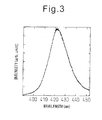
- Fig. 3 shows the PL (photoluminescence) measurement results of the light-emitting layer obtained above. It is seen from Fig. 3 that luminescence with a peak wavelength of 422 nm is obtained and a high-quality light-emitting layer can be formed on the composite substrate for the formation of a light-emitting device produced in Example above.
- the composite substrate for the formation of a light-emitting device of Comparative Example 1 was formed as follows.
- a light-converting material substrate was introduced into the MOCVD chamber, and cleaning and nitridation of the substrate surface were performed under the same conditions as in Example 1 to form a first layer of an AlN layer.
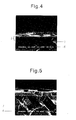
- Fig. 4 shows the cross-sectional SEM photograph of the obtained substrate.
- the white portion 6 is the Y 3 Al 5 O 12 :Ce phase
- the black portion 7 is the Al 2 O 3 phase.
- the first layer 2 formed on the light-converting material substrate forms a flat film on the Al 2 O 3 phase but has large surface unevenness on the Y 3 Al 5 O 12 :Ce phase, revealing a low smoothness (RSM: 5.262 nm).
- RSM 5.262 nm
- a GaN layer was formed by a known method described in Example 1, and further thereon, a light-emitting layer was formed.
- the GaN layer located on the Y 3 Al 5 O 12 :Ce phase was found to be a polycrystalline layer containing many crystal defects such as dislocation and crystal grain boundary.
- the PL (photoluminescence) measurement results revealed that irrespective of the Al 2 O 3 phase and the Y 3 Al 5 O 12 phase, many non-light-emitting regions are present in the light-emitting layer on the phases and the light emission characteristics are bad.
- a light-converting material substrate was introduced into the chamber of an MOCVD apparatus, and cleaning and nitridation of the substrate surface were performed at 1,100°C. Thereafter, the temperature was lowered to 500°C, and a GaN buffer layer was formed on the light-converting material substrate by using an H 2 gas, an N 2 gas, an NH 3 gas and a TMG gas, after the cleaning and nitridation. Subsequently, the temperature was raised to 1,100°C, and a GaN layer (thickness: about 5 ⁇ m) was formed at a growth temperature of 1,100°C by using an H 2 gas, an N 2 gas, an NH 3 gas and a TMG gas.
- Fig. 5 shows the cross-sectional SEM photograph of the obtained GaN layer.
- the white portion 6 is the Y 3 Al 5 O 12 :Ce phase
- the black portion 7 is the Al 2 O 3 phase.
- the GaN layer formed on the light-converting material substrate forms a flat GaN layer on the Al 2 O 3 phase, but a GaN layer cannot be formed on the Y 3 Al 5 O 12 :Ce phase, revealing that a difference in height or a step is produced between the GaN layer on the Al 2 O 3 phase and the GaN layer on the Y 3 Al 5 O 12 phase.
- the substrate for the formation of a light-emitting device, the formation method thereof, and the light-emitting device using the substrate for the formation of a light-emitting device, provided by the present invention are useful in industry.
Landscapes
- Chemical & Material Sciences (AREA)
- Engineering & Computer Science (AREA)
- Ceramic Engineering (AREA)
- Materials Engineering (AREA)
- Organic Chemistry (AREA)
- Manufacturing & Machinery (AREA)
- Structural Engineering (AREA)
- Inorganic Chemistry (AREA)
- Composite Materials (AREA)
- Led Devices (AREA)
- Luminescent Compositions (AREA)
- Chemical Vapour Deposition (AREA)
Abstract
Description
- 0001 The present invention relates to a substrate for the formation of a light-emitting device. More specifically, the present invention relates to a composite substrate for the formation of a light-emitting device, using a light-converting material substrate, and a method for forming the same.
- 0002 Recently, a white light-emitting diode where a blue light-emitting element using a nitride-based compound semiconductor is utilized as the light emission source is being developed and studied, and since this is a lightweight, mercury-free and long-life device, demands therefor are expected to expand in the future. In a currently most common white light-emitting diode device, as described, for example, in
Patent Document 1, a coating layer containing a fluorescent material capable of emitting yellow light by absorbing a part of blue light, and a mold layer for mixing blue light from the light source with yellow light from the coating layer are provided on the entire surface of a light-emitting element capable of emitting blue light, and a pseudo-white color is obtained by mixing blue and yellow colors which are in the complementary color relationship. As the coating layer, a mixture powder of cerium-activated YAG (Y3Al5O12:Ce) powder and epoxy resin has been conventionally employed. However, in this method, when applying the coating layer, for example, distribution unevenness of the contained fluorescent material powder or fluctuation in the amount of the fluorescent material powder among light-emitting diode individuals may occur and in turn, the light-emitting diode suffers from color unevenness. - 0003 In order to avoid such a problem, in Patent Document 2, a white light-emitting diode device obtained by forming a blue diode element having a light-emitting layer composed of InGaN on a substrate with the principal surface being the Al2O3 (0001) plane of a material having a texture where Al2O3 and Y3Al5O12:Ce are continuously and three-dimensionally entangled, has been reported. In the white light emitting diode device of this report, a method of causing blue light emitted from the light-emitting layer to be incident directly on the substrate, allowing transmission of the blue light in the Al2O3 phase, and emitting homogeneous yellow light in the Y3Al5O12:Ce phase, thereby efficiently extracting light only by a light-emitting chip without use of a fluorescent material powder-containing coating layer and obtaining homogeneous white light free from color unevenness, has been proposed.
- 0004
- Patent Document 1: Japanese Unexamined Patent Publication (Kokai) No.
2000-208815 - Patent Document 2:
W02006/043719 - 0005 However, according to the method described in Patent Document 2, a device having characteristics equal to or better than those of the conventional blue light-emitting diode device is difficult to form on the light-converting material substrate by using a known method, and there is a limit to obtain an excellent white light-emitting diode device. Since, different phases, for example, Al2O3 phase and Y3Al5O12 phase, are present in the light-converting material substrate. The substrate used in the conventional blue light-emitting diode device is, for example, sapphire having a similar crystal structure, or GaN having the same crystal structure. Therefore, when a GaN layer is formed on the light-converting material layer by a known technology of forming a nitride compound layer by using sapphire or GaN as the substrate, the GaN layer may be preferentially formed on the Al2O3 phase, but the GaN layer cannot be formed on the Y3Al5O12:Ce phase having a large lattice mismatch ratio with GaN or even if the layer can be formed, surface smoothness or crystallinity is low wand deterioration in the characteristics of the blue light-emitting diode device is incurred.
- 0006 Under these circumstances, in order to solve these problems, an object of the present invention is to provide a composite substrate for the formation of a light-emitting device, ensuring that a high-quality nitride-based light-emitting diode can be easily formed on its top surface and the obtained substrate-attached light-emitting diode functions as a light-emitting device capable of emitting light for an arbitrary color such as white.
- 0007 As a result of continuous and intensive studies on the composite substrate for the formation of a light-emitting deice, the present inventors have found that when an Al-containing nitride layer is formed by a specific method on a light-converting material layer having a texture comprising two or more oxide layers continuously and three-dimensionally entangled with each other, said two or more oxide phases including an Al2O3 phase and at least one fluorescence-emitting oxide phase, a flat AlN layer having little defects is formed on the outermost surface of the layer, a GaN-based light-emitting diode element with excellent emission characteristics can be formed thereon and an excellent light-emitting diode device is obtained. The present invention has been accomplished based on this finding.
- 0008 That is, the present invention relates to a composite substrate for the formation of a light-emitting device, comprising a light-converting material substrate for radiating at least a part of incident light as light different in the wavelength through the surface opposite the incident surface, and at least two or more Al-containing nitride layers formed on the light-converting material substrate, wherein the light-converting material substrate has a texture comprising two or more oxide phases continuously and three-dimensionally entangled with each other, the two or more oxide phases including an Al2O3 phase and at least one fluorescence-emitting oxide phase, the nitride layers have a first layer of an Al-containing nitride layer formed on each oxide phase constituting the light-converting material substrate and a second layer of a continuously continuing AlN layer with a flat and defectless surface formed on the first layer. More specifically, the second layer has a dislocation density of 1×10¹²/cm2 or less and more preferably has a surface roughness (root-mean-square roughness, RMS) of 5 nm or less.
- 0009 In the light-converting material substrate for use in the present invention, each of the first layer and the second layer forms a uniform continuous layer extending across all phases of the two or more oxide phases of the light-converting material substrate. In a preferred embodiment, each of the first layer and the second layer in the light-converting material substrate contains substantially no void.
- 0010 In the present invention, the fluorescence-emitting oxide phase of the light-converting material substrate is Y3Al5O12:Ce phase, and Al2O3 (0001) plane and Y3Al5O12 (111) plane are principal surfaces.
- 0011 In the present invention, the Al-containing nitride layer of the first layer and the AlN layer of the second layer are grown as crystals by the MOCVD method on the light-converting material substrate.
- 0012 In the present invention, the Al-containing nitride layer of the first layer is AlN.
In the present invention, the film thickness of the first layer is from 0.1 to 5 µm.
In the present invention, the film thickness of the second layer is from 2 to 9 µm. - 0013 The present invention also relates to a light-emitting diode device comprising a semiconductor light-emitting layer formed on the composite substrate for the formation of a light-emitting device claimed in
claim 1, the light-emitting diode device having a function of radiating light after wavelength conversion of at least a part of light from the semiconductor light-emitting light through the composite substrate for the formation of a light-emitting device. - 0014 Also, the present invention relates to a light-emitting diode device comprising a semiconductor light-emitting layer capable of emitting blue light on the composite substrate for the formation of a light-emitting device claimed in claim 2, the light-emitting diode device having a function of radiating light after wavelength conversion of a part of light from the semiconductor light-emitting light, together with light from the semiconductor light-emitting layer, through the composite substrate for the formation of a light-emitting device.
- 0015 The present invention relates to a method for producing the above-described composite substrate for the formation of a light-emitting device (claimed in claim 1), comprising
a first step of subjecting a light-converting material substrate having a texture comprising two or more oxide phases continuously and three-dimensionally entangled with each other said two or more oxide phases including an Al2O3 phase and at least one fluorescence-emitting oxide phase, for radiating at least a part of incident light as light different in the wavelength through the surface opposite the incident surface to a heat treatment at 1,000 to 1,300°C in a mixed gas atmosphere of an H2 gas, an N2 gas and an NH3 gas,
a second step of supplying at least an H2 gas, an N2 gas, an NH3 gas and an Al-containing organic metal compound gas on the light-converting material substrate to form a first layer of Al-containing nitride layer, and
a third step of supplying a mixed gas of an H2 gas, an N2 gas, an NH3 gas and an Al-containing organic metal compound gas on the first layer to form a second layer of AlN at 1,350 to 1,480°C. - 0016 In the present invention, the first step, the second step and the third step are performed by the MOCVD method.
- 0017 In the present invention, the molar ratio between N in the NH3 gas and Al in the Al-containing organic metal compound gas in the third step is smaller than the molar ratio between N in the NH3 gas and Al in the Al-containing organic metal compound gas in the second step.
- 0018 In the present invention, the heat treatment time period in the first step is from 10 to 90 minutes.
- 0019 In the present invention, the Al-containing nitride layer is of AlN.
- 0020 The composite substrate for the formation of a light-emitting device of the present invention is a substrate comprising an Al-containing nitride layer and an outermost surface layer of AlN on a light-converting material substrate comprising an Al2O3 phase and an oxide phase containing a fluorescence-emitting activator, and the surface smoothness and crystallinity of the outermost AlN layer are high. Therefore, a high-quality light-emitting diode device capable of emitting light for an arbitrary color can be easily formed using the composite substrate, and the obtained substrate-attached light-emitting diode device can emit light for an arbitrary color with excellent characteristics by way of mixing with the fluorescence of the light-converting material substrate.
- 0021 Also, in the present invention, yellow light emission is exhibited when using Ce as the fluorescence-emitting activator, and white light can be emitted by forming a blue light-emitting diode on the composite substrate for the formation of a light-emitting device, where Ce is used as the activator.
- 0022
-
Fig. 1 is a schematic view of the cross-sectional shape of the composite substrate for the formation of a light-emitting device of the present invention. -
Fig. 2 is a cross-sectional SEM photograph of the composite substrate for the formation of a light-emitting device, showing an embodiment of the present invention. -
Fig. 3 shows the PL measurement results of the light-emitting layer formed on the composite substrate for the formation of a light-emitting device of the present invention. -
Fig. 4 is a cross-sectional SEM photograph of the first layer formed on the light-converting material substrate for Comparison. -
Fig. 5 is a cross-sectional SEM photograph of GaN formed through a GaN buffer layer on the light-converting material substrate for Comparison. - 0023 In an embodiment of the present invention, the composite substrate for the formation of a light-emitting device of the present invention is described.
- 0024 The light-converting material substrate constituting the composite substrate for the formation of a light-emitting device of the present invention is a solidified body formed of at least two or more oxide phases selected from a single metal oxide and a complex metal oxide continuously and three-dimensionally entangled with each other. At least one of the oxide phases in the solidified body is an Al2O3 crystal phase, and at least one of the oxide phases in the solidified body contains a fluorescence-emitting metal element oxide. The Al2O3 crystal phase has a property of allowing transmission of ultraviolet ray, visible light and infrared ray, which are at a wavelength of 200 to 4,000 nm. In the light-converting material substrate constituting the composite substrate for the formation of a light-emitting device of the present invention, at least the Al2O3 crystal phase transmits light (for example, blue light) from a light-emitting layer formed on the substrate, at least one light-emitting layer absorbs light and emits fluorescence (for example, yellow light), the transmitted light and the fluorescence are mixed, and the mixed light (for example, white light) is released (emitted) from the side opposite the light-emitting layer of the light-converting material substrate, i.e., from the light-emitting device.
- 0025 The single metal oxide is an oxide of one kind of a metal, and a complex metal oxide is an oxide of two or more kinds of metals. The light-converting material substrate has a structure where respective oxides are in a single crystal state and three-dimensionally entangled with each other. Examples of the single metal oxide include Al2O3, ZrO2, MgO, SiO2, TiO2, BaO, BeO, CaO, Cr2O3, and a rare earth element oxide such as La2O3, Y2O3, CeO2, Pr6O11, Nd2O3, SM2O3, Gd2O3, Eu2O3, Tb4O7, Dy2O3, Ho2O3, Er2O3, Tm2O3, Yb2O3 and Lu2O3. Examples of the complex metal oxide include LaAlO3, CeAlO3, PrAlO3, NdAlO3, SmAlO3, EuAlO3, GdAlO3, DyAlO3, ErAlO3, Yb4Al2O9, Y3Al5O12, Er3Al5O12, Tb3Al5O12, 11Al2O3·La2O3, 11Al2O3·Nd2O3, 3Dy2O3·5Al2O3, 2Dy2O3·Al2O3, 11Al2O3·Pr2O3, EuAl11O18, 2Gd2O3·Al2O3, 11Al2O3·Sm2O3, Yb3Al5O12, CeAl11O18, and Er4Al2O9.
- 0026 The at least two or more oxide phases selected from a single metal oxide and a complex metal oxide of the light-converting material substrate are not limited in the dimension of each phase on the substrate surface, but, for example, the complex meal oxide phase has a dimension such that the major axis is from tens of µm to hundreds of µm and the minor axis is from several µm to tens of µm.
- 0027 While the light-converting material substrate constituting the present invention is composed of two or more kinds of oxide phases, individual oxide phases differ in the refractive index and therefore, total reflection on the inner surface of the substrate is unlikely to occur due to refraction-reflection in various directions at the interface between oxide phases, so that a high light extraction efficiency can be also obtained. Furthermore, since the light-converting material substrate is a fluorescent material, more uniform fluorescence can be emitted using light from the light-emitting layer in the semiconductor layer.
- 0028 Particularly, in the case where the substrate for the formation of a light-emitting device is used as the substrate for a white light-emitting diode device, a single crystal of garnet-type crystal that is a complex metal oxide where the oxide phase capable of emitting fluorescence is activated with Ce, is preferred. The garnet-type crystal is represented by the structural formula of A3X5O12, and it is more preferred that one or more elements selected from the group consisting of Y, Tb, Sm, Gd, La and Er are contained in A of the structural formula and similarly, one or more elements selected from Al and Ga are contained in X of the structural formula. Above all, Ce-activated Y3Al5O12 emits strong fluorescence and is preferred. In this case, the light-converting material substrate is constituted of an Al2O3 single crystal and a Y3Al5O12:Ce single crystal, where respective oxide phases formed are continuously and three-dimensionally entangled with each other, and the substrate as a whole consists of the two single crystal phases. The cutting direction of this light-converting material is preferably a direction allowing Al2O3 (0001) plane and Y3Al5O12 (111) plane to serve as principal surfaces. In this regard, when a semiconductor layer represented by InxAlyGa1-x-yN (0≤x≤1, 0≤y≤1, 0≤x+y≤1) is formed on the light-converting material substrate, since InxAlyGa1-x-yN (0≤x≤1, 0≤y≤1, 0≤x+y≤1) has a hexagonal crystal structure, the lattice matching between the Al2O3 (0001) plane and the Y3Al5O12 (111) plane is relatively good and a high-quality semiconductor layer can be formed.
- 0029 The first layer constituting the present invention is an Al-containing nitride layer, and the nitride layer may be a single layer or a plurality of layers.
- 0030 By virtue of being an Al-containing nitride layer, the first layer enables a uniform continuous film to be formed across both an Al2O3 phase and an oxide phase containing at least one fluorescence-emitting oxide phase, which are constituting the light-converting material substrate. Here, the uniform continuous film indicates that the first layer is formed on the entire surface of the substrate and a discontinuous region is not present in the first layer (compare the discontinuous layer of
Fig. 5 with the continuous layer ofFigs. 2 and4 ). Also, in the light-converting material substrate for use in the present invention, the first layer forms a uniform continuous layer across all phases of two or more oxide phases of the light-converting material substrate and therefore, when the second layer is formed thereon, the substrate, the first layer and the second layer are continuing over the entire surface of the substrate also in the direction perpendicular to the substrate, preferably allowing for substantially no formation of a void between the substrate and the second layer (a void due to incomplete continuity of the first layer). - 0031 Also, the first layer has a role as a buffer layer when forming the second layer of an AlN layer and by forming the first layer, it is possible to contain no crystal grain boundary in the second layer formed on respective phases of the Al2O3 phase and the Y3Al5O12 phase and form a second layer reduced in the crystal defect such as dislocation and endowed with excellent surface smoothness.
- 0032 The first layer is preferably an Al-containing nitride layer represented by InxAlyGa1-x-yN (0≤x≤1, 0≤y≤1, 0≤x+y≤1), such as AlN, AlGaN and InAlGaN, and among these, the first layer is more preferably a single AlN layer, because a uniform continuous film can be formed across both an Al2O3 phase and an oxide phase containing at least one fluorescence-emitting oxide phase, which are constituting the light-converting material substrate, and an effect of preventing reduction in the surface smoothness or crystallinity of the second layer or semiconductor layer is achieved.
- 0033 If the film thickness of the first layer is 0.1 µm or less, a difference in height is liable to be produced between the Al2O3 phase and another oxide phase and if the film thickness is 5 µm or more, the surface is susceptible to cracking. For this reason, the film thickness of the first layer is preferably from 0.1 to 5 µm and, in particular, when the light-converting material substrate consists of an Al2O3 phase and a Y3Al5O12:Ce phase and the first layer is a single AlN layer, the film thickness is preferably from 3 to 5 µm.
- 0034 The second layer constituting the present invention is AlN. The first layer is provided for the purpose of forming a uniform continuous phase across both an Al2O3 phase and an oxide phase containing at least one fluorescence-emitting oxide phase and is formed under the growth conditions suitable for the purpose, and this yields a tendency that pits, unevenness, defects and the like may be generated on the surface of the first layer and the surface smoothness is reduced (see,
Fig. 4 ). However, according to the present invention, it has been found that when a second layer of AlN is formed on the first layer and the growth conditions of the second layer are adjusted, pits, unevenness, defects and the like generated in the first layer surface are alleviated and a second layer having a surface with a small value of surface roughness (root-mean-square roughness RMS value) indicative of the surface smoothness can be formed and a high-quality semiconductor layer can be also formed on such a second layer, as a result, the characteristics of the light-emitting diode device can be improved. - 0035 In the case where the first layer is a single AlN layer and the second layer is an AlN layer, the first layer and the second layer can be distinguished by the dislocation densities of the first layer and the second layer on an oxide phase other than the Al2O3 phase, constituting the light-converting material substrate, and the first layer has a higher dislocation density than the second layer.
- 0036 In the present invention, the dislocation density of the second layer of AlN may be 1×10¹²/cm2 or less, preferably 1×10¹⁰/cm2 or less, more preferably 1×10⁹/cm2 or less. When the second layer of AlN has such a low dislocation density, a high-quality semiconductor layer, particularly, nitride-based compound semiconductor layer, can be formed on the second layer.
- 0037 In the composite substrate for the formation of a light-emitting device of the present invention, the second layer of AlN preferably has a surface roughness (root-mean-square roughness, RMS) of 5 nm or less, preferably 2 nm or less, more preferably 1 nm or less, still more preferably 0.7 nm or less. When the second layer of AlN has such a low plane smoothness, a high-quality semiconductor layer, particularly, nitride-based compound semiconductor layer, is advantageously formed on the second layer.
- 0038 As for the growth conditions for forming the second layer of AlN having a lower dislocation density than the first layer and having a surface with small surface smoothness, growth conditions where in the second layer, the ratio between the rate at which AlN grows in the direction parallel to the substrate surface and the rate at which it grows in the direction perpendicular to the substrate surface is larger than that in the first layer, are preferred. Furthermore, growth conditions where in the second layer, the rate at which AlN grows in the direction parallel to the substrate surface is higher than the rate at which it grows in the direction perpendicular to the substrate surface are more preferred, and a higher ratio between the rate at which AlN grows in the direction parallel to the substrate surface and the rate at which it grows in the direction perpendicular to the substrate surface is more preferred. By forming the second layer under such AlN growth conditions, pits, unevenness, defects and the like generated in the surface when forming the first layer can be alleviated and a second layer having a surface with excellent surface smoothness can be obtained. Examples of the conditions for realizing the growth where in the second layer, the rate at which AlN grows in the direction parallel to the substrate surface is higher than the rate at which it grows in the direction perpendicular to the substrate surface as compared with the first layer include, for example, the conditions of allowing AlN to grow at a higher temperature than the growth temperature when the first layer is of AlN, and the conditions of making the N/Al ratio (by mol) of the Al raw material and the N raw material in the vapor-phase growth process smaller than the N/Al ratio when the first layer is of AlN.
- 0039 The film thickness of the second layer is preferably from 2 to 9 µm. If the film thickness of the second layer is less than 2 µm, pits or unevenness in the first layer surface may be insufficiently filled and the surface may have low crystallinity or smoothness, whereas if the film thickness exceeds 9 µm, cracks or abnormal nuclei are liable to be generated. In particular, in order to form a second layer having a lower dislocation density (for example, 1×10⁹/cm2 or less) and excellent surface smoothness, the film thickness is preferably from 5 to 7 µm.
- 0040 The light-emitting diode device of the present invention is obtained by forming a semiconductor layer containing a light-emitting layer, on the above-described composite substrate for the formation of a light-emitting device.
- 0041 The semiconductor layer comprising a light-emitting layer is preferably composed of a nitride-based compound semiconductor represented by InxAlyGa1-x-yN (0≤x≤1, 0≤y≤1, 0≤x+y≤1).
- 0042 The light-emitting layer is preferably a nitride layer capable of emitting at least visible light, and new pseudo light can be obtained according to the wavelength of mixed light resulting from mixing of fluorescence after wavelength conversion of visible light on passing through the light-converting material substrate constituting the composite substrate for the formation of a light-emitting device of the present invention, with visible light before conversion. Furthermore, the visible light preferably emits a violet-to-blue color at a wavelength of 400 to 500 nm. In the case where the emission color is a violet-to-blue color, yellow fluorescence is generated from the Y3Al5O12:Ce crystal when light from the light-emitting layer is incident on the Y3Al5O12:Ce single crystal constituting the light-converting material substrate, and the violet-to-blue light transmits as it is through the Al2O3 crystal. These light rays are mixed by the continuous and three-dimensionally interentangled texture in the light-converting material substrate and released, so that homogeneous white color free from color unevenness can be obtained.
- 0043 The production method of the composite substrate for the formation of a light-emitting device of the present invention is described below.
- 0044 In the method for producing the light-converting material constituting the present invention, the solidified body constituting the light-converting material substrate is produced by melting and then solidifying the raw material metal oxide. For example, the solidified body can be obtained by a simple and easy method where a melt charged into a crucible kept at a predetermined temperature is cooled and solidified while controlling the cooling temperature. A solidified body produced by a unidirectional solidification process is most preferred, because by performing unidirectional solidification, the crystal phase contained continuously grows as a single crystal and each phase comes to have a single crystal orientation.
- 0045 In the production method of the composite substrate for the formation of a light-emitting device of the present invention, the formation up to the semiconductor layer of the light-emitting diode device in the following first to third steps can be performed in the same apparatus and therefore, is preferably performed by the MOCVD method.
- 0046 In the case of using the MOCVD method, in the first step, the light-converting material substrate is introduced into an MOCVD apparatus and thereafter, for removing adsorbed gas, dust and the like on the substrate surface, subjected to thermal cleaning at a temperature of 1,000 to 1,300°C for 5 to 15 minutes by flowing an H2 gas and an N2 gas. The temperature during thermal cleaning is set to the formation temperature of the nitride layer on the substrate or a temperature higher than that, whereby the effect on the film quality by degassing or the like at the temperature when forming the nitride layer can be reduced.
- 0047 Thereafter, an H2 gas, an N2 gas and an NH3 gas are flowed at a temperature of 1,000 to 1,300°C and for forming a thin nitride film layer on the substrate surface, a nitridation treatment is performed for approximately from 10 to 120 minutes. This nitride film layer is a layer to be a nucleus when forming an Al-containing nitride layer immediately above the substrate and in particular, when the other oxide phase constituting the light-converting material substrate is the Y3Al5O12:Ce phase, for forming a high-quality nitride layer thereon, a nitridation treatment under the conditions of a pressure of 76 Torr, a temperature of 1,270°C, an H2 gas flow rate of 12 slm, an N2 gas flow rate of 3 slm, an NH3 gas of 50 sccm and 90 minutes is preferred.
- 0048 After the thermal cleaning and nitridation treatment of the light-converting material substrate, as the second step, formation of a first layer of an Al-containing nitride layer is preformed. At this time, InxAlyGa1-x-yN (0≤x≤1, 0<y≤1, 0<x+y≤1) is preferably used for the nitride layer formed immediately above the substrate, and the first layer can be formed at a temperature of 400 to 1,300°C. Particularly, for forming the nitride layer over the entire surface of the light-converting material substrate, the formation temperature is preferably from 1,000 to 1,300°C. Also, the first layer may be, for example, a multilayer film where an AlN buffer layer is formed at a temperature of 400 to 600°C and an AlGaN layer is formed thereon at a desired temperature, or where an AlN buffer layer is formed at a temperature of 400 to 600°C and an AlN layer or the like is formed thereon at a temperature higher than the formation temperature of the buffer layer. In particular, when the phase constituting the light-converting material substrate are an Al2O3 phase and a Y3Al5O12:Ce phase, a single AlN layer is most preferred because a highest-quality film can be formed across both phases, and the conditions when forming the AlN layer depend on the configuration of the MOCVD apparatus and cannot be indiscriminately specified but are in general preferably a pressure of 50 to 100 Torr (6.7×10³ to 1.3×10⁴ Pa), a temperature of 1,000 to 1,300°C, an H2 gas flow rate of 10 to 14 slm, an N2 gas flow rate of 0.5 to 3 slm, an NH3 gas of 20 to 100 sccm, and an aluminum raw material gas such as TMA (trimethylaluminum) gas of 20 to 100 sccm. The aluminum raw material gas may be TEA (triethylaluminum) gas or the like, other than TMA (trimethylaluminum) gas. Above all, conditions of a pressure of 76 Torr, a temperature of 1,270°C, an H2 gas flow rate of 12 slm, an N2 gas flow rate of 3 slm, an NH3 gas of 50 sccm, and a TMA (trimethylaluminum) gas of 50 sccm are preferred.
- 0049 As the third step, a second layer of AlN is formed on the first layer. The second layer of AlN is a layer for reducing the unevenness, pits and dislocation density in the surface of the first layer.
As for the growth conditions when forming the second layer of AlN having a lower dislocation density than the first layer and having a surface with small surface smoothness, as described above, growth conditions where in the second layer, the ratio between the rate at which AlN grows in the direction parallel to the substrate surface and the rate at which it grows in the direction perpendicular to the substrate surface is larger than that in the first layer, are preferred. Furthermore, growth condition where in the second layer, the rate at which AlN grows in the direction parallel to the substrate surface is higher than the rate at which it grows in the direction perpendicular to the substrate surface are more preferred, and a higher ratio between the rate at which AlN grows in the direction parallel to the substrate surface and the rate at which it grows in the direction perpendicular to the substrate surface is more preferred. - 0050 Incidentally, in the method of the present invention, it is important that the molar ratio between N in the NH3 gas and Al in the Al-containing organic metal compound gas when forming the second layer is smaller than the molar ratio between N in the NH3 gas and Al in the Al-containing organic metal compound gas when forming the first layer. Therefore, in general, the ratio of the supply amount of the N raw material gas (NH3 gas) to the supply amount of the aluminum raw material gas (molar ratio of N to Al) when forming AlN as the first layer is preferably from 80 to 110, more preferably from 90 to 100, and the ratio of the supply amount of the N raw material gas (NH3 gas) to the supply amount of the aluminum raw material gas (molar ratio of N to Al) when forming AlN as the second layer is preferably 57 or less, more preferably 19 or less.
- 0051 As for the formation conditions of such AlN, the formation temperature is preferably 1,350 to 1,480°C. In particular, when the first layer is a single AlN layer, the formation conditions of the AlN layer for obtaining a high-quality second layer depend on the configuration of the MOCVD apparatus and cannot be indiscriminately specified but are in general preferably a pressure of 50 to 100 Torr (6.7×10³ to 1.3×10⁴ Pa), a temperature of 1,350 to 1,480°C, an H2 gas flow rate of 4 to 14 slm, an N2 gas flow rate of 0.5 to 3 slm, an NH3 gas of 5 to 20 sccm, and an aluminum raw material gas such as TMA (trimethylaluminum) gas of 20 to 100 sccm. The aluminum raw material gas may be TEM (triethylaluminum) gas or the like, other than TMA (trimethylaluminum) gas. Above all, conditions of a pressure of 76 Torr, a temperature of 1,410°C, an H2 gas flow rate of 12 slm, an N2 gas flow rate of 3 slm, an NH3 gas of 10 sccm, and an aluminum raw material gas such as TMA gas of 50 sccm are preferred.
- 0052 The formation conditions of the second layer are characterized in that, first, the growth temperature is higher compared with the formation conditions of the first layer. Furthermore, the ratio of the supply amount of the N raw material gas (NH3 gas) to the supply amount of the aluminum raw material gas is preferably small. That is, when forming AlN as the second layer, it is preferred that not only the growth temperature is higher but also the NH3 gas and the TMA gas are set to make the molar ratio between nitrogen atom and aluminum atom in the raw materials lower than the molar ratio in the first layer (the N2 gas here is inert and is not a raw material of AlN and therefore, its amount is not taken into consideration). This is because by setting the molar ratio in the formation of AlN for the second layer to be low, a growth mode where the ratio between the rate at which AlN formed grows in the direction parallel to the substrate surface and the rate at which it grows in the direction perpendicular to the substrate surface is larger than that in the first layer is established and furthermore, the creation of growth conditions where the rate at which AlN formed growth in the direction parallel to the substrate surface is larger than the rate at which it grows in the direction perpendicular to the substrate surface is promoted. In turn, the unevenness, pits and dislocation density in the first layer surface can be more suitably reduced, and a second layer free from a crystal grain boundary can be obtained on each oxide layer constituting the light-converging material substrate.
- 0053 For producing a light-emitting diode by using the composite substrate for the formation of a light-emitting device of the present invention, this may be attained by crystal-growing a desired semiconductor layer by a known method on the composite substrate for the formation of a light-emitting device of the present invention. The composite substrate for the formation of a light-emitting device of the present invention is characterized in that by using the second layer as the outermost surface, a desired semiconductor layer can be formed directly thereon, but another layer (intermediate layer) may intervene therebetween.
- 0054 The crystal growth method for the semiconductor layer or the intermediate layer may be any of a liquid phase process, a gas phase process and the like, and in particular, when the nitride layer of the composite substrate for the formation of a light-emitting device of the present invention is formed by the MOCVD method, the semiconductor layer of the light-emitting diode is also preferably formed by the MOCVD method. Furthermore, the nitride layer constituting the composite substrate for the formation of a light-emitting device of the present invention is excellent of in the crystallinity on the surface, the surface smoothness and the like and therefore, enables epitaxial growth of a semiconductor layer represented by InxAlyGa1-x-yN (0≤x≤1, 0≤y≤1, 0≤x+y≤1).
- 0055
- An α-Al2O3 powder (purity: 99.99%) and a Y2O3 powder (purity: 99.999%) were weighed in a molar ratio of 82:18, and a CeO2 powder (purity: 99.99%) is charged, so that Y3Al5O12 produced through the reaction of oxides accounts for 1 mol. These powders were wet-mixed in ethanol for 16 hours by means of a ball mill and then, the ethanol as the solvent was removed using an evaporator to obtain a raw material powder. The raw material powder was preliminarily melted in a vacuum furnace to prepare a raw material for unidirectional solidification.
- 0056 This raw material was directly charged into a molybdenum crucible and after setting the crucible in a unidirectional solidification furnace, the raw material was fused under a pressure of 1.33×10⁻³ Pa (10-5 Torr) . In the same atmosphere, the crucible was moved down at a speed of 5 mm/hour to obtain a solidified body composed of a garnet-type crystal Y3Al5O12:Ce and an α-type aluminum oxide crystal Al2O3.
- 0057 Subsequently, the light-converting material substrate was cut such that the (0001) plane of the Al2O3 crystal and the (111) plane of the Y3Al5O12:Ce crystal serve as principal surfaces. The substrate was then polished and washed to obtain a light-converting material substrate having a thickness of 0.43 mm.
- 0058 The obtained light-converting material substrate was introduced into the chamber of an MOCVD apparatus and after adjusting the pressure therein to 76 Torr (1×10⁴ Pa) in a mixed gas atmosphere at an H2 gas flow rate of 12 slm and an N2 gas flow rate of 3 slm, thermal cleaning of the light-converting material substrate was performed for 5 minutes by raising the temperature to 1,270°C.
Thereafter, the substrate surface was nitrided by flowing an NH3 gas at a flow rate of 50 sccm for 90 minutes. - 0059 After the thermal cleaning and nitridation, a reaction was allowed to proceed on the light-converting material substrate at a growth temperature of 1,270°C under the same pressure for 60 minutes at an H2 gas flow rate of 12 slm, an N2 gas flow rate of 3 slm, an NH3 gas flow rate of 50 sccm and a TMA (trimethylaluminum) gas flow rate of 50 sccm, whereby a first layer of AlN was formed to a thickness of about 5 µm.
- 0060 On the first layer of an AlN layer, a reaction was allowed to proceed at a growth temperature of 1,410°C under the same pressure for 90 minutes at an H2 gas flow rate of 12 slm, an N2 gas flow rate of 3 slm, an NH3 gas flow rate of 10 sccm and a TMA gas flow rate of 50 sccm, whereby a second layer of AlN was formed to a thickness of about 6 µm.
- 0061
Fig. 2 shows the SEM (scanning electron microscope) photograph of the cross-section of the substrate obtained above. In the light-convertingmaterial substrate 1 ofFig. 2 , thewhite portion 6 is the Y3Al5O12:Ce phase, and theblack portion 7 is the Al2O3 phase. It is seen from the cross-sectional SEM photograph of the second layer 3 of AlN formed further on the first layer 2 which is formed on the light-convertingmaterial substrate 1 shown inFig. 2 that by the formation on the light-convertingmaterial substrate 1 under the above-described conditions, the first layer 2 is formed on the Al2O3 phase and the Y3Al5O12:Ce phase and the second layer 3 formed on the first layer 2 forms a continuously continuing layer, thereby flattening the surface. Furthermore, the vicinity of the second layer surface was observed by TEM (transmission electron microscope), as a result, the dislocation density was found to be 1.1×10⁹/cm2 at most, revealing high crystallinity. Also, the surface roughness was measured by AFM (atomic force microscope), and the surface root-mean-square roughness (RSM) was found to be 0.69 nm. - 0062 On the obtained composite substrate for the formation of a light-emitting device, a GaN layer was formed using an H2 gas, an NH3 gas and a TMG (trimethylgallium) gas by a known method according to the MOCVD method, and further thereon, a three-layer quantum well structure-type light-emitting layer comprising an InGaN well layer and a barrier layer was formed using an H2 gas, an N2 gas, an NH3 gas, a TMG gas and a TMI (trimethylindium) gas.
- 0063
Fig. 3 shows the PL (photoluminescence) measurement results of the light-emitting layer obtained above. It is seen fromFig. 3 that luminescence with a peak wavelength of 422 nm is obtained and a high-quality light-emitting layer can be formed on the composite substrate for the formation of a light-emitting device produced in Example above. - 0064
- For confirming the effect of Example above, the composite substrate for the formation of a light-emitting device of Comparative Example 1 was formed as follows.
- 0065 First, a light-converting material substrate was introduced into the MOCVD chamber, and cleaning and nitridation of the substrate surface were performed under the same conditions as in Example 1 to form a first layer of an AlN layer.
- 0066
Fig. 4 shows the cross-sectional SEM photograph of the obtained substrate. In the Figure, thewhite portion 6 is the Y3Al5O12:Ce phase, and theblack portion 7 is the Al2O3 phase. It is seen fromFig. 4 that the first layer 2 formed on the light-converting material substrate forms a flat film on the Al2O3 phase but has large surface unevenness on the Y3Al5O12:Ce phase, revealing a low smoothness (RSM: 5.262 nm). Also, the vicinity of the first layer surface was observed by TEM, as a result, the dislocation density could not be evaluated due to many dislocations. - 0067 On the composite substrate for the formation of a light-emitting device obtained in Comparative Example 1, a GaN layer was formed by a known method described in Example 1, and further thereon, a light-emitting layer was formed.
- 0068 As a result of TEM observation, the GaN layer located on the Y3Al5O12:Ce phase was found to be a polycrystalline layer containing many crystal defects such as dislocation and crystal grain boundary. Also, the PL (photoluminescence) measurement results revealed that irrespective of the Al2O3 phase and the Y3Al5O12 phase, many non-light-emitting regions are present in the light-emitting layer on the phases and the light emission characteristics are bad.
- 0069
- For confirming the effect of Example above, without using the production method of the composite substrate for the formation of a light-emitting device of the present invention, formation of a GaN layer on a light-converting material substrate and formation of a three-layer quantum well structure-type light-emitting layer comprising an InGaN well layer and a barrier layer on the GaN layer were attempted as Comparative Example 2 by the following known method.
- 0070 First, a light-converting material substrate was introduced into the chamber of an MOCVD apparatus, and cleaning and nitridation of the substrate surface were performed at 1,100°C. Thereafter, the temperature was lowered to 500°C, and a GaN buffer layer was formed on the light-converting material substrate by using an H2 gas, an N2 gas, an NH3 gas and a TMG gas, after the cleaning and nitridation. Subsequently, the temperature was raised to 1,100°C, and a GaN layer (thickness: about 5 µm) was formed at a growth temperature of 1,100°C by using an H2 gas, an N2 gas, an NH3 gas and a TMG gas.
- 0071
Fig. 5 shows the cross-sectional SEM photograph of the obtained GaN layer. In the Figure, thewhite portion 6 is the Y3Al5O12:Ce phase, and theblack portion 7 is the Al2O3 phase. It is seen fromFig. 5 that the GaN layer formed on the light-converting material substrate forms a flat GaN layer on the Al2O3 phase, but a GaN layer cannot be formed on the Y3Al5O12:Ce phase, revealing that a difference in height or a step is produced between the GaN layer on the Al2O3 phase and the GaN layer on the Y3Al5O12 phase. - 0072 Reduction in the light emission characteristics is apparent from these results and therefore, formation of a light-emitting layer on the GaN layer was not performed.
- 0073 It is evident that the substrate for the formation of a light-emitting device, the formation method thereof, and the light-emitting device using the substrate for the formation of a light-emitting device, provided by the present invention, are useful in industry.
- 0074
- 1
- Light-converting material substrate
- 2
- First layer
- 3
- Second layer
- 4
- Semiconductor layer
- 5
- Composite substrate for the formation of a light- emitting device
- 6
- Y3Al5O12:Ce Phase
- 7
- Al2O3 Phase
Claims (16)
- A composite substrate for the formation of a light-emitting device, comprising a light-converting material substrate for radiating at least a part of incident light as light different in the wavelength through the surface opposite the incident surface, and at least two or more Al-containing nitride layers formed on said light-converting material substrate, wherein said light-converting material substrate has a texture comprising two or more oxide phases continuously and three-dimensionally entangled with each other said two or more oxide phases including an Al2O3 phase and at least one fluorescence-emitting oxide phase, and said nitride layers have a first layer of an Al-containing nitride layer formed on the light-converting material substrate and a second layer of AlN having a dislocation density of 1×10¹²/cm2 or less.
- The composite substrate for the formation of a light-emitting device as claimed in claim 1, wherein each of said first layer and said second layer forms a uniform continuous layer on said two or more oxide phases of said light-converting material substrate to extend across all phases and contains substantially no void.
- The composite substrate for the formation of a light-emitting device as claimed in claim 1 or 2, wherein said second layer has a surface roughness (root-mean-square roughness, RMS) of 5 nm or less.
- The composite substrate for the formation of a light-emitting device as claimed in any one of claims 1 to 3, wherein the fluorescence-emitting oxide phase of said light-converting material substrate is Y3Al5O12:Ce phase.
- The composite substrate for the formation of a light-emitting device as claimed in claim 4, wherein (0001) of said Al2O3 crystal and (111) of said Y3Al5O12:Ce crystal serve as principal surfaces of said light-converting material substrate.
- The composite substrate for the formation of a light-emitting device as claimed in any one of claims 1 to 5, wherein the Al-containing nitride layer of said first layer and the AlN layer of said second layer are grown as crystals by the MOCVD method on said light-converting material substrate.
- The composite substrate for the formation of a light-emitting device as claimed in any one of claims 1 to 6, wherein the Al-containing nitride layer of said first layer is AlN.
- The composite substrate for the formation of a light-emitting device as claimed in claim 7, wherein the film thickness of said first layer is from 0.5 to 5 µm.
- The composite substrate for the formation of a light-emitting device as claimed in claim 7 or 8, wherein the film thickness of said second layer is from 4 to 9 µm.
- A light-emitting diode device comprising a semiconductor light-emitting layer formed on said composite substrate for the formation of a light-emitting device claimed in any one of claims 1 to 9, wherein said light-emitting diode device has a function of radiating light after wavelength conversion of at least a part of light from the semiconductor light-emitting light through said composite substrate for the formation of a light-emitting device.
- A light-emitting diode device comprising a semiconductor light-emitting layer capable of emitting blue light on said composite substrate for the formation of a light-emitting device claimed in any one of claims 4 to 9, wherein said light-emitting diode device has a function of radiating light after wavelength conversion of a part of light from said semiconductor light-emitting light, together with light from said semiconductor light-emitting layer, through said composite substrate for the formation of a light-emitting device.
- A method for producing said composite substrate for the formation of a light-emitting device claimed in any one of claims 1 to 9, comprising
a first step of subjecting a light-converting material substrate having a texture comprising two or more oxide phases continuously and three-dimensionally entangled with each other said two or more phases including an Al2O3 phase and at least one fluorescence-emitting oxide phase, for radiating at least a part of incident light as light different in the wavelength through the surface opposite the incident surface to a heat treatment at 1,000 to 1,300°C in a mixed gas atmosphere of an H2 gas, an N2 gas and an NH3 gas,
a second step of supplying at least an H2 gas, an N2 gas, an NH3 gas and an Al-containing organic metal compound gas on said light-converting material substrate to form a first layer of an Al-containing nitride layer, and
a third step of supplying a mixed gas of an H2 gas, an N2 gas, an NH3 gas and an Al-containing organic metal compound gas on said first layer at 1,350 to 1,480°C to form a second layer of AlN. - The method for producing the composite substrate for the formation of a light-emitting device as claimed in claim 12, wherein said first step, said second step and said third step are performed by the MOCVD method.
- The method for producing the composite substrate for the formation of a light-emitting device as claimed in claim 12 or 13, wherein the molar ratio between N in the NH3 gas and Al in the Al-containing organic metal compound gas in said third step is smaller than the molar ratio between N in the NH3 gas and Al in the Al-containing organic metal compound gas in said second step.
- The method for producing the composite substrate for the formation of a light-emitting device as claimed in any one of claims 12 to 14, wherein the heat treatment time period in said first step is from 10 to 90 minutes.
- The method for producing the composite substrate for the formation of a light-emitting device as claimed in any one of claims 12 to 15, wherein said Al-containing nitride layer is of AlN.
Applications Claiming Priority (2)
| Application Number | Priority Date | Filing Date | Title |
|---|---|---|---|
| JP2009049833 | 2009-03-03 | ||
| PCT/JP2010/053727 WO2010101272A1 (en) | 2009-03-03 | 2010-03-02 | Composite substrate for forming light-emitting device, light emitting diode device, and method of producing same |
Publications (2)
| Publication Number | Publication Date |
|---|---|
| EP2405498A1 true EP2405498A1 (en) | 2012-01-11 |
| EP2405498A4 EP2405498A4 (en) | 2013-12-04 |
Family
ID=42709822
Family Applications (1)
| Application Number | Title | Priority Date | Filing Date |
|---|---|---|---|
| EP10748863.7A Withdrawn EP2405498A4 (en) | 2009-03-03 | 2010-03-02 | COMPOSITE SUBSTRATE FOR LIGHT EMITTING DEVICE FORMATION, LIGHT EMITTING DEVICE DEVICE AND METHOD FOR MANUFACTURING SAME |
Country Status (5)
| Country | Link |
|---|---|
| US (1) | US8686455B2 (en) |
| EP (1) | EP2405498A4 (en) |
| JP (1) | JP5649005B2 (en) |
| KR (2) | KR20110113655A (en) |
| WO (1) | WO2010101272A1 (en) |
Cited By (1)
| Publication number | Priority date | Publication date | Assignee | Title |
|---|---|---|---|---|
| EP2830104A1 (en) * | 2013-07-22 | 2015-01-28 | Fujian Institute Of Research On The Structure Of Matter, Chinese Academy Of Sciences | Gan based led epitaxial structure and method for manufacturing the same |
Families Citing this family (12)
| Publication number | Priority date | Publication date | Assignee | Title |
|---|---|---|---|---|
| JP5668339B2 (en) * | 2010-06-30 | 2015-02-12 | 住友電気工業株式会社 | Manufacturing method of semiconductor device |
| DE102011012298A1 (en) * | 2010-12-28 | 2012-06-28 | Osram Opto Semiconductors Gmbh | Composite substrate, composite substrate semiconductor chip and method of manufacturing composite substrates and semiconductor chips |
| JP6144630B2 (en) * | 2012-08-30 | 2017-06-07 | 日本碍子株式会社 | Method for producing composite substrate, method for producing functional layer made of group 13 element nitride |
| KR20140032811A (en) * | 2012-09-07 | 2014-03-17 | 삼성전자주식회사 | Backlight unit and liquid crystal display having the same |
| JP6040898B2 (en) * | 2013-09-09 | 2016-12-07 | 豊田合成株式会社 | III-nitride semiconductor light emitting device manufacturing method and manufacturing apparatus, and substrate cleaning method |
| US9460917B2 (en) * | 2014-02-12 | 2016-10-04 | Translucent, Inc. | Method of growing III-N semiconductor layer on Si substrate |
| DE102015101330A1 (en) * | 2015-01-29 | 2016-08-04 | Osram Opto Semiconductors Gmbh | Device for converting the wavelength of an electromagnetic radiation |
| JP6810406B2 (en) * | 2016-12-06 | 2021-01-06 | 株式会社サイオクス | Nitride semiconductor template manufacturing method |
| JP2018155968A (en) * | 2017-03-17 | 2018-10-04 | 日亜化学工業株式会社 | Method for manufacturing translucent member and method for manufacturing light emitting device |
| US20210151314A1 (en) * | 2017-12-19 | 2021-05-20 | Sumco Corporation | Method for manufacturing group iii nitride semiconductor substrate |
| KR102752047B1 (en) * | 2021-10-28 | 2025-01-09 | 삼성전자주식회사 | Micro light emitting device and display apparatus including the same |
| CN117567146A (en) * | 2023-11-17 | 2024-02-20 | 江苏师范大学 | High-heat-resistance composite structure fluorescent ceramic for laser illumination and preparation method thereof |
Family Cites Families (11)
| Publication number | Priority date | Publication date | Assignee | Title |
|---|---|---|---|---|
| JP2999435B2 (en) * | 1996-06-14 | 2000-01-17 | 松下電器産業株式会社 | Semiconductor manufacturing method and semiconductor light emitting device |
| TW383508B (en) | 1996-07-29 | 2000-03-01 | Nichia Kagaku Kogyo Kk | Light emitting device and display |
| JP3505405B2 (en) | 1998-10-22 | 2004-03-08 | 三洋電機株式会社 | Semiconductor device and method of manufacturing the same |
| US6744076B2 (en) * | 2002-03-14 | 2004-06-01 | The Circle For The Promotion Of Science And Engineering | Single crystalline aluminum nitride film, method of forming the same, base substrate for group III element nitride film, light emitting device and surface acoustic wave device |
| JP4178410B2 (en) * | 2003-11-26 | 2008-11-12 | サンケン電気株式会社 | Semiconductor light emitting device |
| JP4316454B2 (en) * | 2004-09-10 | 2009-08-19 | 株式会社東芝 | Semiconductor substrate, semiconductor element, semiconductor element manufacturing method, and semiconductor substrate manufacturing method |
| JP4586802B2 (en) | 2004-10-21 | 2010-11-24 | 宇部興産株式会社 | Light emitting diode element, light emitting diode substrate, and method for manufacturing light emitting diode element |
| JP4653671B2 (en) | 2005-03-14 | 2011-03-16 | 株式会社東芝 | Light emitting device |
| JP5041397B2 (en) * | 2006-04-26 | 2012-10-03 | 豊田合成株式会社 | Manufacturing method of semiconductor substrate for electronic device |
| TW200741044A (en) * | 2006-03-16 | 2007-11-01 | Toyoda Gosei Kk | Semiconductor substrate, electronic device, optical device, and production methods therefor |
| JP2007329177A (en) * | 2006-06-06 | 2007-12-20 | Harison Toshiba Lighting Corp | Optical element and light emitting device |
-
2010
- 2010-03-02 KR KR1020117020628A patent/KR20110113655A/en not_active Ceased
- 2010-03-02 KR KR1020137029464A patent/KR101371557B1/en not_active Expired - Fee Related
- 2010-03-02 US US13/203,853 patent/US8686455B2/en not_active Expired - Fee Related
- 2010-03-02 WO PCT/JP2010/053727 patent/WO2010101272A1/en not_active Ceased
- 2010-03-02 EP EP10748863.7A patent/EP2405498A4/en not_active Withdrawn
- 2010-03-02 JP JP2011502832A patent/JP5649005B2/en not_active Expired - Fee Related
Cited By (1)
| Publication number | Priority date | Publication date | Assignee | Title |
|---|---|---|---|---|
| EP2830104A1 (en) * | 2013-07-22 | 2015-01-28 | Fujian Institute Of Research On The Structure Of Matter, Chinese Academy Of Sciences | Gan based led epitaxial structure and method for manufacturing the same |
Also Published As
| Publication number | Publication date |
|---|---|
| EP2405498A4 (en) | 2013-12-04 |
| WO2010101272A1 (en) | 2010-09-10 |
| JP5649005B2 (en) | 2015-01-07 |
| KR20130126758A (en) | 2013-11-20 |
| JPWO2010101272A1 (en) | 2012-09-10 |
| US8686455B2 (en) | 2014-04-01 |
| KR20110113655A (en) | 2011-10-17 |
| US20120025252A1 (en) | 2012-02-02 |
| KR101371557B1 (en) | 2014-03-10 |
Similar Documents
| Publication | Publication Date | Title |
|---|---|---|
| US8686455B2 (en) | Composite substrate for formation of light-emitting device, light-emitting diode device and manufacturing method thereof | |
| KR101036530B1 (en) | LED Substrate and LED | |
| EP2743382B1 (en) | Method for peeling group 13 element nitride film | |
| US7935973B2 (en) | Light-emitting diode, light-emitting diode substrate and production method of light-emitting diode | |
| US20130157445A1 (en) | POLYCRYSTALLINE ALUMINUM NITRIDE BASE MATERIAL FOR CRYSTAL GROWTH OF GaN-BASE SEMICONDUCTOR AND METHOD FOR MANUFACTURING GaN-BASE SEMICONDUCTOR USING THE SAME | |
| CN108699728B (en) | Self-supporting substrate containing polycrystalline Group 13 element nitride and light-emitting element using the self-supporting substrate | |
| CN105393336A (en) | Composite substrate, manufacturing method thereof, functional element, and seed crystal substrate | |
| JP5388068B2 (en) | COMPOSITE SUBSTRATE FOR LIGHT EMITTING ELEMENT FORMATION AND MANUFACTURING METHOD THEREOF | |
| JP4269645B2 (en) | Nitride semiconductor LED element using substrate containing activator, and growth method | |
| JP2016188169A (en) | POLYCRYSTALLINE ALUMINUM NITRIDE BASE MATERIAL FOR GROWING GaN BASED SEMICONDUCTOR CRYSTAL AND MANUFACTURING METHOD OF GaN BASED SEMICONDUCTOR USING THE SUBSTRATE | |
| JP4032704B2 (en) | Nitride semiconductor device | |
| US10472735B2 (en) | Method of making a single crystal wavelength conversion element, single crystal wavelength conversion element, and light source containing same | |
| JP5366079B2 (en) | COMPOSITE SUBSTRATE FOR LIGHT EMITTING ELEMENT FORMATION, LIGHT EMITTING DIODE ELEMENT AND MANUFACTURING METHOD THEREOF | |
| CN108291329A (en) | 13 race's element nitride crystal substrates and function element | |
| WO2014084105A1 (en) | Composite substrate and functional element | |
| US11035055B2 (en) | Group 13 nitride layer, composite substrate, and functional element | |
| JP2006315951A (en) | Electronic element and thin-film substrate |
Legal Events
| Date | Code | Title | Description |
|---|---|---|---|
| PUAI | Public reference made under article 153(3) epc to a published international application that has entered the european phase |
Free format text: ORIGINAL CODE: 0009012 |
|
| 17P | Request for examination filed |
Effective date: 20110831 |
|
| AK | Designated contracting states |
Kind code of ref document: A1 Designated state(s): AT BE BG CH CY CZ DE DK EE ES FI FR GB GR HR HU IE IS IT LI LT LU LV MC MK MT NL NO PL PT RO SE SI SK SM TR |
|
| RAP1 | Party data changed (applicant data changed or rights of an application transferred) |
Owner name: UBE INDUSTRIES, LTD. |
|
| DAX | Request for extension of the european patent (deleted) | ||
| A4 | Supplementary search report drawn up and despatched |
Effective date: 20131106 |
|
| RIC1 | Information provided on ipc code assigned before grant |
Ipc: H01L 33/50 20100101ALI20131030BHEP Ipc: H01L 33/32 20100101AFI20131030BHEP Ipc: C04B 35/44 20060101ALI20131030BHEP |
|
| 17Q | First examination report despatched |
Effective date: 20140625 |
|
| GRAP | Despatch of communication of intention to grant a patent |
Free format text: ORIGINAL CODE: EPIDOSNIGR1 |
|
| INTG | Intention to grant announced |
Effective date: 20170120 |
|
| STAA | Information on the status of an ep patent application or granted ep patent |
Free format text: STATUS: THE APPLICATION IS DEEMED TO BE WITHDRAWN |
|
| 18D | Application deemed to be withdrawn |
Effective date: 20170531 |