EP2405327A1 - Integrated touch control device - Google Patents
Integrated touch control device Download PDFInfo
- Publication number
- EP2405327A1 EP2405327A1 EP09841011A EP09841011A EP2405327A1 EP 2405327 A1 EP2405327 A1 EP 2405327A1 EP 09841011 A EP09841011 A EP 09841011A EP 09841011 A EP09841011 A EP 09841011A EP 2405327 A1 EP2405327 A1 EP 2405327A1
- Authority
- EP
- European Patent Office
- Prior art keywords
- electrode pattern
- substrate
- touch
- touch device
- electrode
- Prior art date
- Legal status (The legal status is an assumption and is not a legal conclusion. Google has not performed a legal analysis and makes no representation as to the accuracy of the status listed.)
- Withdrawn
Links
Images





Classifications
-
- G—PHYSICS
- G06—COMPUTING OR CALCULATING; COUNTING
- G06F—ELECTRIC DIGITAL DATA PROCESSING
- G06F3/00—Input arrangements for transferring data to be processed into a form capable of being handled by the computer; Output arrangements for transferring data from processing unit to output unit, e.g. interface arrangements
- G06F3/01—Input arrangements or combined input and output arrangements for interaction between user and computer
- G06F3/03—Arrangements for converting the position or the displacement of a member into a coded form
- G06F3/041—Digitisers, e.g. for touch screens or touch pads, characterised by the transducing means
-
- G—PHYSICS
- G06—COMPUTING OR CALCULATING; COUNTING
- G06F—ELECTRIC DIGITAL DATA PROCESSING
- G06F3/00—Input arrangements for transferring data to be processed into a form capable of being handled by the computer; Output arrangements for transferring data from processing unit to output unit, e.g. interface arrangements
- G06F3/01—Input arrangements or combined input and output arrangements for interaction between user and computer
- G06F3/03—Arrangements for converting the position or the displacement of a member into a coded form
- G06F3/041—Digitisers, e.g. for touch screens or touch pads, characterised by the transducing means
- G06F3/045—Digitisers, e.g. for touch screens or touch pads, characterised by the transducing means using resistive elements, e.g. a single continuous surface or two parallel surfaces put in contact
-
- G—PHYSICS
- G06—COMPUTING OR CALCULATING; COUNTING
- G06F—ELECTRIC DIGITAL DATA PROCESSING
- G06F3/00—Input arrangements for transferring data to be processed into a form capable of being handled by the computer; Output arrangements for transferring data from processing unit to output unit, e.g. interface arrangements
- G06F3/01—Input arrangements or combined input and output arrangements for interaction between user and computer
- G06F3/03—Arrangements for converting the position or the displacement of a member into a coded form
- G06F3/041—Digitisers, e.g. for touch screens or touch pads, characterised by the transducing means
- G06F3/044—Digitisers, e.g. for touch screens or touch pads, characterised by the transducing means by capacitive means
-
- G—PHYSICS
- G06—COMPUTING OR CALCULATING; COUNTING
- G06F—ELECTRIC DIGITAL DATA PROCESSING
- G06F3/00—Input arrangements for transferring data to be processed into a form capable of being handled by the computer; Output arrangements for transferring data from processing unit to output unit, e.g. interface arrangements
- G06F3/01—Input arrangements or combined input and output arrangements for interaction between user and computer
- G06F3/03—Arrangements for converting the position or the displacement of a member into a coded form
- G06F3/041—Digitisers, e.g. for touch screens or touch pads, characterised by the transducing means
- G06F3/044—Digitisers, e.g. for touch screens or touch pads, characterised by the transducing means by capacitive means
- G06F3/0445—Digitisers, e.g. for touch screens or touch pads, characterised by the transducing means by capacitive means using two or more layers of sensing electrodes, e.g. using two layers of electrodes separated by a dielectric layer
-
- G—PHYSICS
- G06—COMPUTING OR CALCULATING; COUNTING
- G06F—ELECTRIC DIGITAL DATA PROCESSING
- G06F3/00—Input arrangements for transferring data to be processed into a form capable of being handled by the computer; Output arrangements for transferring data from processing unit to output unit, e.g. interface arrangements
- G06F3/01—Input arrangements or combined input and output arrangements for interaction between user and computer
- G06F3/03—Arrangements for converting the position or the displacement of a member into a coded form
- G06F3/041—Digitisers, e.g. for touch screens or touch pads, characterised by the transducing means
- G06F3/044—Digitisers, e.g. for touch screens or touch pads, characterised by the transducing means by capacitive means
- G06F3/0446—Digitisers, e.g. for touch screens or touch pads, characterised by the transducing means by capacitive means using a grid-like structure of electrodes in at least two directions, e.g. using row and column electrodes
-
- G—PHYSICS
- G06—COMPUTING OR CALCULATING; COUNTING
- G06F—ELECTRIC DIGITAL DATA PROCESSING
- G06F2203/00—Indexing scheme relating to G06F3/00 - G06F3/048
- G06F2203/041—Indexing scheme relating to G06F3/041 - G06F3/045
- G06F2203/04103—Manufacturing, i.e. details related to manufacturing processes specially suited for touch sensitive devices
-
- G—PHYSICS
- G06—COMPUTING OR CALCULATING; COUNTING
- G06F—ELECTRIC DIGITAL DATA PROCESSING
- G06F2203/00—Indexing scheme relating to G06F3/00 - G06F3/048
- G06F2203/041—Indexing scheme relating to G06F3/041 - G06F3/045
- G06F2203/04106—Multi-sensing digitiser, i.e. digitiser using at least two different sensing technologies simultaneously or alternatively, e.g. for detecting pen and finger, for saving power or for improving position detection
-
- G—PHYSICS
- G06—COMPUTING OR CALCULATING; COUNTING
- G06F—ELECTRIC DIGITAL DATA PROCESSING
- G06F2203/00—Indexing scheme relating to G06F3/00 - G06F3/048
- G06F2203/041—Indexing scheme relating to G06F3/041 - G06F3/045
- G06F2203/04112—Electrode mesh in capacitive digitiser: electrode for touch sensing is formed of a mesh of very fine, normally metallic, interconnected lines that are almost invisible to see. This provides a quite large but transparent electrode surface, without need for ITO or similar transparent conductive material
-
- G—PHYSICS
- G06—COMPUTING OR CALCULATING; COUNTING
- G06F—ELECTRIC DIGITAL DATA PROCESSING
- G06F2203/00—Indexing scheme relating to G06F3/00 - G06F3/048
- G06F2203/041—Indexing scheme relating to G06F3/041 - G06F3/045
- G06F2203/04113—Peripheral electrode pattern in resistive digitisers, i.e. electrodes at the periphery of the resistive sheet are shaped in patterns enhancing linearity of induced field
Definitions
- the present invention relates to a touch device, and in particular to a touch device integrated with capacitive and resistive operation for being selectively operated in a capacitive touch position detection mode and a resistive touch position detection mode.
- a resistive touch panel comprises an ITO (Indium-Tin-Oxide) film and a sheet of ITO glass, which are spaced from each other by a plurality of insulation spacers.
- ITO Indium-Tin-Oxide
- a touching object such as a stylus
- a local depression is formed, which makes a contact with the ITO glass located therebelow thereby inducing a variation of voltage, which, through conversion from analog signal into digital signal, is applied to a microprocessor to be processed for calculation and determination of the operation position of the touched point.
- a capacitive touch panel generally makes use of variation of electrical capacity coupling between a transparent electrodes and a conductor to generate an induced current by which the operation position of a touched point can be determined.
- the outermost layer is a thin transparent substrate
- the second layer is an ITO layer.
- the resistive touch panel and the capacitive touch panel both suffer certain limitations on the operations thereof and have drawbacks.
- the resistive touch panel although having an advantage of low cost, needs to cause physical contact between two conductive layers on the upper and lower sides in the operation thereof. Thus, a pressure must be applied to quite an extent. This often leads to damage of the conductive layers. Also, the sensitivity is low.
- a capacitive touch panel due to the operation principle thereof, must be operated with a touching object that is a conductor, such as a user's finger or a touch head, in order to conduct electric current therethrough. The capacitive touch panel cannot be operated with an insulative touching object.
- an objective of the present invention is to provide a touch device integrated with capacitive and resistive operation, which detects the ways how a user touches the touch device and in response thereto, switches the operation thereof between capacitive and resistive touch position detection modes.
- the touch device when a user slightly touches a touch operation surface of the touch device, the touch device operates in the capacitive touch position detection mode, and when the user forcibly depresses the touch operation surface of the touch device or carries out a hand writing input operation on the touch operation surface of the touch device, the touch device operates in a resistive touch position detection mode.
- a touch device integrated with capacitive and resistive sensing operation which comprises a first substrate on which a first electrode pattern is formed and a second substrate on which a second electrode pattern is formed.
- the first and second electrode patterns are respectively connected to a microprocessor via a first scanning circuit and a second scanning circuit.
- the touch device When a user slightly touches a touch operation surface of the touch device, the touch device is set in a capacitive touch position detection mode in which a change of electrical capacitive coupling between the touching object and the first electrode pattern is applied to the microprocessor for determination of at least one operation position where the touching object operates on the touch operation surface of the first substrate.
- the first substrate is depressed at an operation position, causing the first electrode pattern and the second electrode pattern to contact each other, whereby the touch device is set in a resistive touch position detection mode in which the microprocessor determines at least one operation position where the touching object operates on the touch operation surface of the first substrate according to variation of voltage in the second electrode pattern.
- the touch device integrated with capacitive and resistive operation in accordance with the present invention is operable in the touch operation mode of either a capacitive touch panel or a resistive touch panel. Constraint in the touching object usable in the conventional resistive touch panel or the capacitive touch panel can be eliminated and the touch control operation of the touch device is simplified.
- the touch device can be selectively operated in the best touch control mode in accordance with different ways of operation and possesses the advantages of the touch panels of both types.
- the present invention is also particularly suitable in the applications where hand writing input is applied to the touch device to effectively solve the problems of unsmooth hand writing input and poor detection result found in the conventional capacitive touch panels.
- Figure 1 shows a system block diagram of a first embodiment in accordance with the present invention
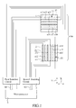
- Figure 2 shows an exploded view of major constituent components of Figure 1 ;
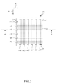
- Figure 3 shows relative positional relationship between a first electrode pattern and a second electrode pattern after a first substrate and a second substrate of Figure 1 are bonded together;
- Figure 4 shows a cross-sectional view taken along line 4-4 of Figure 3 ;
- Figure 5 schematically demonstrates a touch device in accordance with the present invention being operated by a user's finger
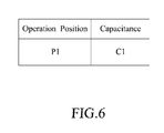
- Figure 6 shows a table listing capacitance corresponding to a touched position demonstrated in Figure 5 ;
- Figure 7 schematically shows the touch device in accordance with the first embodiment of the present invention being operated with a touching object
- Figure 8 shows a system block diagram of a second embodiment in accordance with the present invention.
- Figure 9 shows a circuit diagram demonstrating a depression operation applied to the touch device of the second embodiment of the present invention.
- Figure 10 shows an equivalent circuit of Figure 9 .
- Figure 11 schematically shows the touch device in accordance with the second embodiment of the present invention being operated with a touching object.
- a touch device integrated with capacitive and resistive sensing operation in accordance with the present invention comprises a first substrate 1, which comprises an insulation film, such as a PET (Polyethylene Terephthalate) film, of which a transparent material can be selected in a practical application.
- the first substrate 1 comprises a first electrode bonding surface 11 and a touch operation surface 12.
- the first electrode bonding surface 11 of the first substrate 1 forms a first electrode pattern 13.
- the first electrode pattern 13 comprises a plurality of strip-like electrodes s11 , s12, s13, s14, s15, s16, which are substantially parallel to and spaced from each other by a given distance and extend along a first axis X.
- the first electrode pattern 13 is primarily made of electrically conductive material.
- the electrically conductive substance can be for example ITO (Indium Tin Oxide), which forms a transparent electrically-conductive layer.
- the strip-like electrodes s11 , s12, s13, s14, s15, s16 are connected via a first scanning circuit 4 to a microprocessor 3 to be controlled by the microprocessor 3 so that a predetermined driving voltage can be applied to the strip-like electrodes s11 , s12, s13, s14, s15, s16, or alternatively, the first scanning circuit 4 carries out scanning to detect the variation of electrical capacitive coupling of the strip-like electrodes s11 , s12, s13, s14, s15, s16 and issues a scanning detection signal S1 obtained thereby to the microprocessor 3 for subsequent processing.
- a second substrate 2 comprises a second electrode bonding surface 21 opposing the first electrode bonding surface 11 of the first substrate 1.
- the second electrode bonding surface 21 of the second substrate 2 forms thereon a second electrode pattern 22.
- the second electrode pattern 22 comprises a plurality of strip-like electrodes s11', s12', s13', s14', s15', s16' , which are substantially parallel to and are spaced from each other by a predetermined distance and extend along a second axis Y.
- the second substrate 2 is set at a location substantially opposing the first substrate 1 to have the second electrode pattern 22 facing the first electrode pattern 13.
- a predetermined distance d is defined between the first electrode pattern 13 of the first substrate 1 and the second electrode pattern 22 of the second substrate 2 (as shown in Figure 4 ).
- the strip-like electrodes s11', s12', s13', s14', s15', s16' are connected via a second scanning circuit 5 to the microprocessor 3 for scanning and detecting variation of voltage occurring in each of the strip-like electrodes s11', s12', s13', s14', s15', s16' and a scanning detection signal S2 is issued to the microprocessor 3 for subsequent processing.
- each strip-like electrode s11', s12', s13', s14', s15', s16' can be connected to the second scanning circuit 5 by one end or by both ends.
- the strip-like electrodes s11, s12, s13, s14, s15, s16 of the first electrode pattern 13 are formed on the first electrode bonding surface 11 of the first substrate 1 in an arrangement of being substantially parallel to and spaced from each other.
- the first electrode pattern 13 and the second electrode pattern 22 are each illustratively comprised six strip-like electrodes, but it is apparent that the number of the strip-like electrodes is not limited to this and more or less strip-like electrodes can be employed.
- the strip-like electrodes s11, s12, s13, s14, s15, s16 of the first electrode pattern 13 and the strip-like electrodes s11', s12', s13', s14', s15', s16' of the second electrode pattern 22 are set in an right angle intersecting and overlapping arrangement.
- the first substrate 1 and the second substrate 2 sandwich therebetween a plurality of insulation spacers 6 to maintain a predetermined distance between the first substrate 1 and the second substrate 2 after they are bonded together, whereby direct contact between the first electrode pattern 13 of the first substrate 1 and the second electrode pattern 22 of the second substrate 2 can be prevented.
- Figure 5 demonstrates the touch device of the present invention is operated by a user's finger and Figure 6 shows a table listing the capacitance corresponding to each touch position demonstrated in Figure 5 . As shown, the example illustrated is used to explain the touch control operation applied to the touch device 100 by means of a touching object 7.
- an operation position occurring at the intersection between the strip-like electrode s13 of the first electrode pattern 13 and the strip-like electrode s12' of the second electrode pattern 22 is referred to as operation position P1 .
- a touching object 7 that is employed to operate the touch device 100 can be for example a finger, a conductive object, or other suitable operating objects.
- the touch device 100 When the touching object 7 slightly touches a touched position on the touch operation surface 12 of the first substrate 1 to such an extent that the first electrode pattern 13 does not get into physical contact with the second electrode pattern 22 (such as the operation position P1 shown in Figure 5 ), under this condition, the touch device 100 is operated with a capacitive touch position detection mode, where the touching object 7 and the strip-like electrode s13 of the first electrode pattern 13 induce a capacitance C1 (see Figure 6 ) therebetween due to electrical capacity coupling.
- the first scanning circuit 4 through scanning each strip-like electrode s11, s12, s13, s14, s15, s16 of the first substrate 1, detects the variation of electrical capacity coupling between the touching object 7 and the first electrode pattern 13 and issues the first scanning detection signal S1 to the microprocessor 3.
- FIG. 7 is a schematic view illustrating that the touch device of the first embodiment of the present invention is operated with a touching object.
- a touching object 7a used in the instant example is a conductive object or a non-conductive object (such as a touch stylus or other suitable objects).
- the touch device 100 is operated with a resistive touch position detection mode, wherein a driving voltage is applied to the strip-like electrode s13' and the touch device 100 calculates the operation position of the touching object 7a operating on the touch operation surface 12 of the first substrate 1 according to variation of voltage in the strip-like electrode s13' of the second electrode pattern 22.
- the second embodiment comprises major constituent components that are identical to the counterparts of the first embodiment and the identical components are designated with the same reference numerals.
- the second embodiment comprises a first substrate 1a that has a first electrode bonding surface 11a and the first electrode bonding surface 11a forms thereon a first electrode pattern 13a that comprises an ITO transparent conductive layer having a continuous planar structure.
- Four corners of the first electrode pattern 13a are connected to the first scanning circuit 4 in order to allow a driving voltage to be applied thereto to form a voltage gradient in the first electrode pattern 13a .
- FIGs 9 and 10 are respectively a circuit diagram demonstrating a depression operation applied to the touch device 100a and an equivalent circuit thereof, as shown in Figure 9 , when the touch device 100a is being depressed at an operation position P2, a resistance R1 , R2, R3, R4 is induced between the operation position P2 and each corner.
- a resistance R1 , R2, R3, R4 is induced between the operation position P2 and each corner.
- a corresponding current I1, I2 , I3 , I4 can be calculated, and based on the ratio between the currents I1 , I2 , I3 , I4 , the location of the operation position P2 on the touch device 100a can be calculated.
- a touching object 7a that is employed to operate the touch device 100a can be a conductive object or a non-conductive object (such as a touch stylus or other suitable objects).
- the touch device 100a is operated with a resistive touch position detection mode, wherein the first scanning circuit 4 applies a driving voltage to the first electrode pattern 13a and the driving voltage is transmitted from the first electrode pattern 13a to the strip-like electrode s13' of the second electrode pattern 22.
- the second scanning circuit 5 performs scanning and detection and then issues a scanning detection signal S2 to the microprocessor 3.
- the microprocessor 3 responds to the variation of voltage in the strip-like electrode s13' of the second electrode pattern 22 and calculates the touched position of the touching object 7a on the first substrate 1.
Landscapes
- Engineering & Computer Science (AREA)
- General Engineering & Computer Science (AREA)
- Theoretical Computer Science (AREA)
- Human Computer Interaction (AREA)
- Physics & Mathematics (AREA)
- General Physics & Mathematics (AREA)
- Position Input By Displaying (AREA)
Abstract
Description
- The present invention relates to a touch device, and in particular to a touch device integrated with capacitive and resistive operation for being selectively operated in a capacitive touch position detection mode and a resistive touch position detection mode.
- A resistive touch panel comprises an ITO (Indium-Tin-Oxide) film and a sheet of ITO glass, which are spaced from each other by a plurality of insulation spacers. When a touching object (such as a stylus) touches and depresses the ITO film, a local depression is formed, which makes a contact with the ITO glass located therebelow thereby inducing a variation of voltage, which, through conversion from analog signal into digital signal, is applied to a microprocessor to be processed for calculation and determination of the operation position of the touched point.
- A capacitive touch panel generally makes use of variation of electrical capacity coupling between a transparent electrodes and a conductor to generate an induced current by which the operation position of a touched point can be determined. In the structure of the capacitive touch panel, the outermost layer is a thin transparent substrate, and the second layer is an ITO layer. When a touching object (such as a user's finger) is put in touch with the surface of the transparent substrate, the touching object induces electrical capacity coupling with the electric field on the outer conductive layer, leading to a minute variation of current. A microprocessor may then perform calculation to determine the operation position where the figure touches.
- However, the resistive touch panel and the capacitive touch panel both suffer certain limitations on the operations thereof and have drawbacks. The resistive touch panel, although having an advantage of low cost, needs to cause physical contact between two conductive layers on the upper and lower sides in the operation thereof. Thus, a pressure must be applied to quite an extent. This often leads to damage of the conductive layers. Also, the sensitivity is low. On the other hand, although having high sensitivity, a capacitive touch panel, due to the operation principle thereof, must be operated with a touching object that is a conductor, such as a user's finger or a touch head, in order to conduct electric current therethrough. The capacitive touch panel cannot be operated with an insulative touching object.
- Thus, an objective of the present invention is to provide a touch device integrated with capacitive and resistive operation, which detects the ways how a user touches the touch device and in response thereto, switches the operation thereof between capacitive and resistive touch position detection modes. Thus, when a user slightly touches a touch operation surface of the touch device, the touch device operates in the capacitive touch position detection mode, and when the user forcibly depresses the touch operation surface of the touch device or carries out a hand writing input operation on the touch operation surface of the touch device, the touch device operates in a resistive touch position detection mode.
- The technical solution that the present invention adopts to overcome the above discussed problems is a touch device integrated with capacitive and resistive sensing operation, which comprises a first substrate on which a first electrode pattern is formed and a second substrate on which a second electrode pattern is formed. The first and second electrode patterns are respectively connected to a microprocessor via a first scanning circuit and a second scanning circuit.
- When a user slightly touches a touch operation surface of the touch device, the touch device is set in a capacitive touch position detection mode in which a change of electrical capacitive coupling between the touching object and the first electrode pattern is applied to the microprocessor for determination of at least one operation position where the touching object operates on the touch operation surface of the first substrate.
- When the user forcibly depresses the touch operation surface of the touch device or carries out a hand writing input operation on the touch operation surface of the touch device, the first substrate is depressed at an operation position, causing the first electrode pattern and the second electrode pattern to contact each other, whereby the touch device is set in a resistive touch position detection mode in which the microprocessor determines at least one operation position where the touching object operates on the touch operation surface of the first substrate according to variation of voltage in the second electrode pattern.
- With the technical solution adopted in the present invention, the touch device integrated with capacitive and resistive operation in accordance with the present invention, together with a simple circuit structure, when integrated with a simple scanning detection process, is operable in the touch operation mode of either a capacitive touch panel or a resistive touch panel. Constraint in the touching object usable in the conventional resistive touch panel or the capacitive touch panel can be eliminated and the touch control operation of the touch device is simplified. The touch device can be selectively operated in the best touch control mode in accordance with different ways of operation and possesses the advantages of the touch panels of both types.
- The present invention is also particularly suitable in the applications where hand writing input is applied to the touch device to effectively solve the problems of unsmooth hand writing input and poor detection result found in the conventional capacitive touch panels.
- The present invention will be apparent to those skilled in the art by reading the following description of preferred embodiments thereof with reference to the drawings, in which:
-
Figure 1 shows a system block diagram of a first embodiment in accordance with the present invention; -
Figure 2 shows an exploded view of major constituent components ofFigure 1 ; -
Figure 3 shows relative positional relationship between a first electrode pattern and a second electrode pattern after a first substrate and a second substrate ofFigure 1 are bonded together; -
Figure 4 shows a cross-sectional view taken along line 4-4 ofFigure 3 ; -
Figure 5 schematically demonstrates a touch device in accordance with the present invention being operated by a user's finger; -
Figure 6 shows a table listing capacitance corresponding to a touched position demonstrated inFigure 5 ; -
Figure 7 schematically shows the touch device in accordance with the first embodiment of the present invention being operated with a touching object; -
Figure 8 shows a system block diagram of a second embodiment in accordance with the present invention; -
Figure 9 shows a circuit diagram demonstrating a depression operation applied to the touch device of the second embodiment of the present invention; -
Figure 10 shows an equivalent circuit ofFigure 9 ; and -
Figure 11 schematically shows the touch device in accordance with the second embodiment of the present invention being operated with a touching object. - With reference to the drawings and in particular to
Figures 1 and2 , a system block diagram of a first embodiment in accordance with the present invention is illustrated.Figure 2 shows an exploded view of major constituent components ofFigure 1 . As shown, a touch device integrated with capacitive and resistive sensing operation in accordance with the present invention, generally designated at 100, comprises a first substrate 1, which comprises an insulation film, such as a PET (Polyethylene Terephthalate) film, of which a transparent material can be selected in a practical application. The first substrate 1 comprises a firstelectrode bonding surface 11 and atouch operation surface 12. The firstelectrode bonding surface 11 of the first substrate 1 forms afirst electrode pattern 13. Thefirst electrode pattern 13 comprises a plurality of strip-like electrodes s11, s12, s13, s14, s15, s16, which are substantially parallel to and spaced from each other by a given distance and extend along a first axis X. Thefirst electrode pattern 13 is primarily made of electrically conductive material. The electrically conductive substance can be for example ITO (Indium Tin Oxide), which forms a transparent electrically-conductive layer. - The strip-like electrodes s11, s12, s13, s14, s15, s16 are connected via a first scanning circuit 4 to a
microprocessor 3 to be controlled by themicroprocessor 3 so that a predetermined driving voltage can be applied to the strip-like electrodes s11, s12, s13, s14, s15, s16, or alternatively, the first scanning circuit 4 carries out scanning to detect the variation of electrical capacitive coupling of the strip-like electrodes s11, s12, s13, s14, s15, s16 and issues a scanning detection signal S1 obtained thereby to themicroprocessor 3 for subsequent processing. - A
second substrate 2 comprises a secondelectrode bonding surface 21 opposing the firstelectrode bonding surface 11 of the first substrate 1.. The secondelectrode bonding surface 21 of thesecond substrate 2 forms thereon asecond electrode pattern 22. Thesecond electrode pattern 22 comprises a plurality of strip-like electrodes s11', s12', s13', s14', s15', s16', which are substantially parallel to and are spaced from each other by a predetermined distance and extend along a second axis Y. Thesecond substrate 2 is set at a location substantially opposing the first substrate 1 to have thesecond electrode pattern 22 facing thefirst electrode pattern 13. A predetermined distance d is defined between thefirst electrode pattern 13 of the first substrate 1 and thesecond electrode pattern 22 of the second substrate 2 (as shown inFigure 4 ). - The strip-like electrodes s11', s12', s13', s14', s15', s16' are connected via a second scanning circuit 5 to the
microprocessor 3 for scanning and detecting variation of voltage occurring in each of the strip-like electrodes s11', s12', s13', s14', s15', s16' and a scanning detection signal S2 is issued to themicroprocessor 3 for subsequent processing. In practical applications, each strip-like electrode s11', s12', s13', s14', s15', s16' can be connected to the second scanning circuit 5 by one end or by both ends. - The strip-like electrodes s11, s12, s13, s14, s15, s16 of the
first electrode pattern 13 are formed on the firstelectrode bonding surface 11 of the first substrate 1 in an arrangement of being substantially parallel to and spaced from each other. On local areas between thefirst electrode pattern 13 and the secondelectrode bonding surface 21 of thesecond substrate 2 where no strip-like electrode s11', s12', s13', s14', s15', s16' is set, at least oneinsulation spacer 6 is provided. With theinsulation spacers 6, direct contact between thefirst electrode pattern 13 and thesecond electrode pattern 22 can be prevented. - Referring to
Figure 3 , which shows the relative positional relationship between thefirst electrode pattern 13 and thesecond electrode pattern 22 after the first substrate 1 is bonded to thesecond substrate 2, in the embodiment illustrated, thefirst electrode pattern 13 and thesecond electrode pattern 22 are each illustratively comprised six strip-like electrodes, but it is apparent that the number of the strip-like electrodes is not limited to this and more or less strip-like electrodes can be employed. In a preferred embodiment of the present invention, the strip-like electrodes s11, s12, s13, s14, s15, s16 of thefirst electrode pattern 13 and the strip-like electrodes s11', s12', s13', s14', s15', s16' of thesecond electrode pattern 22 are set in an right angle intersecting and overlapping arrangement. - Referring to
Figure 4 , the first substrate 1 and thesecond substrate 2 sandwich therebetween a plurality ofinsulation spacers 6 to maintain a predetermined distance between the first substrate 1 and thesecond substrate 2 after they are bonded together, whereby direct contact between thefirst electrode pattern 13 of the first substrate 1 and thesecond electrode pattern 22 of thesecond substrate 2 can be prevented. - Referring to
Figures 5 and6 ,Figure 5 demonstrates the touch device of the present invention is operated by a user's finger andFigure 6 shows a table listing the capacitance corresponding to each touch position demonstrated inFigure 5 . As shown, the example illustrated is used to explain the touch control operation applied to thetouch device 100 by means of a touching object 7. - Firstly, in the example illustrated, an operation position occurring at the intersection between the strip-like electrode s13 of the
first electrode pattern 13 and the strip-like electrode s12' of thesecond electrode pattern 22 is referred to as operation position P1. In the example illustrated, a touching object 7 that is employed to operate thetouch device 100 can be for example a finger, a conductive object, or other suitable operating objects. - When the touching object 7 slightly touches a touched position on the
touch operation surface 12 of the first substrate 1 to such an extent that thefirst electrode pattern 13 does not get into physical contact with the second electrode pattern 22 (such as the operation position P1 shown inFigure 5 ), under this condition, thetouch device 100 is operated with a capacitive touch position detection mode, where the touching object 7 and the strip-like electrode s13 of thefirst electrode pattern 13 induce a capacitance C1 (seeFigure 6 ) therebetween due to electrical capacity coupling. The first scanning circuit 4, through scanning each strip-like electrode s11, s12, s13, s14, s15, s16 of the first substrate 1, detects the variation of electrical capacity coupling between the touching object 7 and thefirst electrode pattern 13 and issues the first scanning detection signal S1 to themicroprocessor 3. -
Figure 7 is a schematic view illustrating that the touch device of the first embodiment of the present invention is operated with a touching object. As shown, a touchingobject 7a used in the instant example is a conductive object or a non-conductive object (such as a touch stylus or other suitable objects). When thetouching object 7a depresses thetouch operation surface 12 of the first substrate 1, due to the depression of the first substrate 1 at the operation position, the strip-like electrode s13 of thefirst electrode pattern 13 and the strip-like electrode s13' of thesecond electrode pattern 22 get into contact with each other (the predetermined distance d becoming d=0). Under this condition, thetouch device 100 is operated with a resistive touch position detection mode, wherein a driving voltage is applied to the strip-like electrode s13' and thetouch device 100 calculates the operation position of thetouching object 7a operating on thetouch operation surface 12 of the first substrate 1 according to variation of voltage in the strip-like electrode s13' of thesecond electrode pattern 22. - Referring to
Figure 8 , which shows a system block diagram in accordance with a second embodiment of the present invention, the second embodiment comprises major constituent components that are identical to the counterparts of the first embodiment and the identical components are designated with the same reference numerals. A difference is that the second embodiment comprises a first substrate 1a that has a firstelectrode bonding surface 11a and the firstelectrode bonding surface 11a forms thereon afirst electrode pattern 13a that comprises an ITO transparent conductive layer having a continuous planar structure. Four corners of thefirst electrode pattern 13a are connected to the first scanning circuit 4 in order to allow a driving voltage to be applied thereto to form a voltage gradient in thefirst electrode pattern 13a. - Referring to
Figures 9 and 10 , which are respectively a circuit diagram demonstrating a depression operation applied to thetouch device 100a and an equivalent circuit thereof, as shown inFigure 9 , when thetouch device 100a is being depressed at an operation position P2, a resistance R1, R2, R3, R4 is induced between the operation position P2 and each corner. As shown inFigure 9 , based on the voltage Vs1, Vs2, Vs3, Vs4 supplied and the corresponding resistance R1, R2, R3, R4, a corresponding current I1, I2, I3, I4 can be calculated, and based on the ratio between the currents I1, I2, I3, I4, the location of the operation position P2 on thetouch device 100a can be calculated. - Referring to
Figure 11 , which shows a schematic view of the touch device of the present invention being operated with a touching object, firstly, an operation position occurring at the intersection between thefirst electrode pattern 13a and the strip-like electrode s13' of thesecond electrode pattern 22 is referred to as operation position P3. In the instant example, a touchingobject 7a that is employed to operate thetouch device 100a can be a conductive object or a non-conductive object (such as a touch stylus or other suitable objects). - Also referring to
Figure 8 , when a user uses thetouching object 7a to forcibly depress the first substrate 1a in a given touching direction I, due to the depression of the first substrate 1a at the operation position P3, thefirst electrode pattern 13a and the strip-like electrode s13' of thesecond electrode pattern 22 get into contact with each other (the predetermined distance d becoming d=0). Under this condition, thetouch device 100a is operated with a resistive touch position detection mode, wherein the first scanning circuit 4 applies a driving voltage to thefirst electrode pattern 13a and the driving voltage is transmitted from thefirst electrode pattern 13a to the strip-like electrode s13' of thesecond electrode pattern 22. The second scanning circuit 5 performs scanning and detection and then issues a scanning detection signal S2 to themicroprocessor 3. Themicroprocessor 3 responds to the variation of voltage in the strip-like electrode s13' of thesecond electrode pattern 22 and calculates the touched position of thetouching object 7a on the first substrate 1. - Although the present invention has been described with reference to the preferred embodiments thereof, it is apparent to those skilled in the art that a variety of modifications and changes may be made without departing from the scope of the present invention which is intended to be defined by the appended claims.
Claims (7)
- A touch device adapted to detect a touch control movement that a touching object applied to the touch device, the touch device comprising:a first substrate, which has a first electrode bonding surface and a touch operation surface;a first electrode pattern, which is formed on the first electrode bonding surface of the first substrate;a second substrate, which is arranged at a location opposing the first substrate and has a second electrode bonding surface facing the first electrode bonding surface of the first substrate, the first substrate and the second substrate being spaced from each other by a predetermined distance;a second electrode pattern, which is formed on the second electrode bonding surface of the second substrate and opposes the first electrode pattern; anda microprocessor, which is electrically connected to the first electrode pattern and the second electrode pattern;wherein when the touching object slightly touches the touch operation surface of the first substrate, the touch device is set in a capacitive touch position detection mode in which a change of electrical capacitive coupling between the touching object and the first electrode pattern is applied to the microprocessor for determination of at least one operation position where the touching object operates on the touch operation surface of the first substrate; andwherein when the touching object forcibly depresses the touch operation surface of the first substrate or when a hand writing input operation is performed on the touch operation surface of the first substrate, the first substrate is depressed at an operation position, causing the first electrode pattern and the second electrode pattern to contact each other, whereby the touch device is set in a resistive touch position detection mode in which the microprocessor determines at least one operation position where the touching object operates on the touch operation surface of the first substrate according to variation of voltage in the second electrode pattern.
- The touch device as claimed in Claim 1, wherein the first electrode pattern and the second electrode pattern each comprise a plurality of strip-like electrodes that are parallel to and spaced from each other.
- The touch device as claimed in Claim 2, wherein the strip-like electrodes of the first electrode pattern are connected to the microprocessor via a first scanning circuit and wherein the strip-like electrodes of the second electrode pattern are connected to the microprocessor via a second scanning circuit.
- The pressure detectable touch device as claimed in Claim 2, wherein the first electrode pattern and the conductive layer are spaced from each other by insulation spacers.
- The touch device as claimed in Claim 1, wherein the first electrode pattern comprises a continuous planar structure and wherein the second electrode pattern comprises a plurality of strip-like electrodes that are parallel to and spaced from each other.
- The touch device as claimed in Claim 5, wherein the first electrode pattern is connected to the microprocessor via a first scanning circuit and wherein the strip-like electrodes of the second electrode pattern are connected to the microprocessor via a second scanning circuit.
- The pressure detectable touch device as claimed in Claim 5, wherein the first electrode pattern and the conductive layer are spaced from each other by insulation spacers.
Applications Claiming Priority (2)
| Application Number | Priority Date | Filing Date | Title |
|---|---|---|---|
| CN2009100080927A CN101825961B (en) | 2009-03-03 | 2009-03-03 | Integrated touch device |
| PCT/CN2009/072589 WO2010099678A1 (en) | 2009-03-03 | 2009-07-01 | Integrated touch control device |
Publications (2)
| Publication Number | Publication Date |
|---|---|
| EP2405327A1 true EP2405327A1 (en) | 2012-01-11 |
| EP2405327A4 EP2405327A4 (en) | 2014-05-21 |
Family
ID=42689904
Family Applications (1)
| Application Number | Title | Priority Date | Filing Date |
|---|---|---|---|
| EP09841011.1A Withdrawn EP2405327A4 (en) | 2009-03-03 | 2009-07-01 | Integrated touch control device |
Country Status (6)
| Country | Link |
|---|---|
| US (1) | US20120086668A1 (en) |
| EP (1) | EP2405327A4 (en) |
| JP (1) | JP5536808B2 (en) |
| KR (1) | KR101402883B1 (en) |
| CN (1) | CN101825961B (en) |
| WO (1) | WO2010099678A1 (en) |
Cited By (3)
| Publication number | Priority date | Publication date | Assignee | Title |
|---|---|---|---|---|
| WO2012085293A3 (en) * | 2010-12-23 | 2012-08-30 | Polyic Gmbh & Co. Kg | Transparent multi-touch sensor and method for producing same |
| EP3147764A1 (en) * | 2015-09-25 | 2017-03-29 | Fujitsu Component Limited | Touch panel device |
| CN104106028B (en) * | 2012-02-15 | 2018-02-09 | 富士通电子零件有限公司 | Touch panel and position detection method |
Families Citing this family (25)
| Publication number | Priority date | Publication date | Assignee | Title |
|---|---|---|---|---|
| CN101833387B (en) * | 2009-03-13 | 2013-09-11 | 宸鸿光电科技股份有限公司 | Pressure sensitive touch device |
| KR20120028553A (en) * | 2010-09-15 | 2012-03-23 | 삼성전자주식회사 | Operation method for touch panel, portable device including the same and operation method thereof |
| US8988384B2 (en) * | 2011-09-23 | 2015-03-24 | Apple Inc. | Force sensor interface for touch controller |
| TWI471794B (en) * | 2011-10-20 | 2015-02-01 | Wintek Corp | Touch panel |
| US9246486B2 (en) | 2011-12-16 | 2016-01-26 | Apple Inc. | Electronic device with noise-cancelling force sensor |
| JP2013168032A (en) * | 2012-02-15 | 2013-08-29 | Fujitsu Component Ltd | Touch panel and position detection method |
| JP2013175058A (en) * | 2012-02-24 | 2013-09-05 | Fujitsu Component Ltd | Touch panel and position detection method |
| JP2013168033A (en) * | 2012-02-15 | 2013-08-29 | Fujitsu Component Ltd | Touch panel and position detection method |
| WO2013149331A1 (en) | 2012-04-07 | 2013-10-10 | Cambridge Touch Technologies, Ltd. | Pressure sensing display device |
| CN103941109B (en) * | 2013-01-21 | 2017-07-28 | 宸鸿科技(厦门)有限公司 | The test device of contact panel |
| KR102089607B1 (en) | 2013-05-28 | 2020-03-17 | 삼성디스플레이 주식회사 | Display device |
| US9442599B2 (en) * | 2013-07-25 | 2016-09-13 | Atmel Corporation | System and method for using signals resulting from signal transmission in a touch sensor |
| CN108415634B (en) * | 2013-08-30 | 2020-12-15 | 烟台正海科技股份有限公司 | Touch device |
| CN104516597A (en) * | 2013-09-30 | 2015-04-15 | 升达科技股份有限公司 | Device integrating capacitive touch and resistive touch and operation method thereof |
| GB2533667B (en) | 2014-12-23 | 2017-07-19 | Cambridge Touch Tech Ltd | Pressure-sensitive touch panel |
| KR102480003B1 (en) | 2014-12-23 | 2022-12-21 | 케임브리지 터치 테크놀로지스 리미티드 | Pressure sensitive touch panel |
| TW201709040A (en) * | 2015-08-24 | 2017-03-01 | 達鴻先進科技股份有限公司 | Flexible touch panel device |
| US10282046B2 (en) | 2015-12-23 | 2019-05-07 | Cambridge Touch Technologies Ltd. | Pressure-sensitive touch panel |
| GB2544353B (en) | 2015-12-23 | 2018-02-21 | Cambridge Touch Tech Ltd | Pressure-sensitive touch panel |
| CN106125408A (en) * | 2016-08-31 | 2016-11-16 | 京东方科技集团股份有限公司 | The driving method of array base palte, display device and display device |
| GB2565305A (en) | 2017-08-08 | 2019-02-13 | Cambridge Touch Tech Ltd | Device for processing signals from a pressure-sensing touch panel |
| US11093088B2 (en) | 2017-08-08 | 2021-08-17 | Cambridge Touch Technologies Ltd. | Device for processing signals from a pressure-sensing touch panel |
| US10572061B2 (en) * | 2018-05-28 | 2020-02-25 | Higgstec Inc. | Hybrid touch module |
| US20210109615A1 (en) * | 2019-10-14 | 2021-04-15 | RET Equipment Inc. | Resistive pressure sensor device system |
| US11175755B1 (en) * | 2020-06-08 | 2021-11-16 | Wacom Co., Ltd. | Input system and input method |
Family Cites Families (12)
| Publication number | Priority date | Publication date | Assignee | Title |
|---|---|---|---|---|
| KR100300397B1 (en) * | 1994-04-21 | 2001-10-22 | 김순택 | System having touch panel and digitizer function and driving method |
| JP2002287902A (en) | 2001-01-17 | 2002-10-04 | Seiko Epson Corp | Touch panel and electronic equipment |
| JP4124444B2 (en) * | 2003-01-30 | 2008-07-23 | 富士通コンポーネント株式会社 | Touch panel, input device having the same, and electronic device |
| JP4920396B2 (en) * | 2006-12-15 | 2012-04-18 | 三菱電機株式会社 | Touch panel control device |
| JP2008165575A (en) * | 2006-12-28 | 2008-07-17 | Mitsubishi Electric Corp | Touch panel device |
| CN201060480Y (en) * | 2007-03-09 | 2008-05-14 | 洋华光电股份有限公司 | Combined touch control inductor |
| CN101261552A (en) * | 2007-03-09 | 2008-09-10 | 洋华光电股份有限公司 | Combined touch control induction device |
| US20080231605A1 (en) * | 2007-03-21 | 2008-09-25 | Kai-Ti Yang | Compound touch panel |
| US20080316182A1 (en) * | 2007-06-21 | 2008-12-25 | Mika Antila | Touch Sensor and Method for Operating a Touch Sensor |
| JP2009015685A (en) * | 2007-07-06 | 2009-01-22 | Meiji Univ | Touch panel device and operation information generation method thereof |
| EP2026179A1 (en) * | 2007-08-10 | 2009-02-18 | IEE International Electronics & Engineering S.A.R.L. | Method of generating input data |
| TWI394067B (en) * | 2008-06-20 | 2013-04-21 | Multi - sensor touchpad |
-
2009
- 2009-03-03 CN CN2009100080927A patent/CN101825961B/en not_active Expired - Fee Related
- 2009-07-01 KR KR1020117022409A patent/KR101402883B1/en not_active Expired - Fee Related
- 2009-07-01 US US13/254,457 patent/US20120086668A1/en not_active Abandoned
- 2009-07-01 EP EP09841011.1A patent/EP2405327A4/en not_active Withdrawn
- 2009-07-01 JP JP2011552303A patent/JP5536808B2/en not_active Expired - Fee Related
- 2009-07-01 WO PCT/CN2009/072589 patent/WO2010099678A1/en not_active Ceased
Cited By (4)
| Publication number | Priority date | Publication date | Assignee | Title |
|---|---|---|---|---|
| WO2012085293A3 (en) * | 2010-12-23 | 2012-08-30 | Polyic Gmbh & Co. Kg | Transparent multi-touch sensor and method for producing same |
| CN104106028B (en) * | 2012-02-15 | 2018-02-09 | 富士通电子零件有限公司 | Touch panel and position detection method |
| EP3147764A1 (en) * | 2015-09-25 | 2017-03-29 | Fujitsu Component Limited | Touch panel device |
| US9952714B2 (en) | 2015-09-25 | 2018-04-24 | Fujitsu Component Limited | Touch panel device |
Also Published As
| Publication number | Publication date |
|---|---|
| JP2012519337A (en) | 2012-08-23 |
| JP5536808B2 (en) | 2014-07-02 |
| US20120086668A1 (en) | 2012-04-12 |
| KR101402883B1 (en) | 2014-06-03 |
| CN101825961B (en) | 2013-11-06 |
| EP2405327A4 (en) | 2014-05-21 |
| KR20120001737A (en) | 2012-01-04 |
| WO2010099678A1 (en) | 2010-09-10 |
| CN101825961A (en) | 2010-09-08 |
Similar Documents
| Publication | Publication Date | Title |
|---|---|---|
| US20120086668A1 (en) | Integrated touch control device | |
| EP2407864A1 (en) | Pressure sensitive touch control device | |
| JP5685411B2 (en) | Touch panel | |
| US9354714B2 (en) | Keypad with integrated touch sensitive apparatus | |
| US9019216B2 (en) | Touch panel and method of detecting coordinate position | |
| US8106891B2 (en) | Multi-point touch-sensitive device | |
| CN101526864B (en) | Touch panel | |
| CN101901090A (en) | Display device | |
| KR20100022059A (en) | Touch sensor and method for operating a touch sensor | |
| KR20040056745A (en) | Touch panel | |
| JP2010055612A (en) | Multi-point touch-sensitive system | |
| KR20130126228A (en) | Matrix switching type touch screen panel having pressure sensor | |
| US20100033436A1 (en) | Touch-Controlled Liquid Crystal Display and Touch Panel thereof | |
| TWI395121B (en) | Pressure detectable touch device | |
| CN201436625U (en) | Pressure sensing type touch control structure | |
| CN101493743A (en) | Touch panel and driving method thereof | |
| US20110285664A1 (en) | Resistive touch panel and input device using the same | |
| CN102890589B (en) | Conductive pattern structure and construction method of capacitive touch panel | |
| CN201556183U (en) | Integrated touch control structure | |
| JP2013175058A (en) | Touch panel and position detection method | |
| KR101494259B1 (en) | Composite touch pannel with appendix and method for detecting touch using therefor | |
| TWI402734B (en) | Touch device integrated with capacitive and resistive sensing operation | |
| US20230176681A1 (en) | Hovering touch panel and hovering touch device | |
| JP4333062B2 (en) | Input device and electronic device using the same | |
| CN101847053B (en) | Screen body of touch screen |
Legal Events
| Date | Code | Title | Description |
|---|---|---|---|
| PUAI | Public reference made under article 153(3) epc to a published international application that has entered the european phase |
Free format text: ORIGINAL CODE: 0009012 |
|
| 17P | Request for examination filed |
Effective date: 20110913 |
|
| AK | Designated contracting states |
Kind code of ref document: A1 Designated state(s): AT BE BG CH CY CZ DE DK EE ES FI FR GB GR HR HU IE IS IT LI LT LU LV MC MK MT NL NO PL PT RO SE SI SK SM TR |
|
| DAX | Request for extension of the european patent (deleted) | ||
| A4 | Supplementary search report drawn up and despatched |
Effective date: 20140422 |
|
| RIC1 | Information provided on ipc code assigned before grant |
Ipc: G06F 3/044 20060101AFI20140414BHEP Ipc: G06F 3/045 20060101ALI20140414BHEP |
|
| STAA | Information on the status of an ep patent application or granted ep patent |
Free format text: STATUS: THE APPLICATION IS DEEMED TO BE WITHDRAWN |
|
| 18D | Application deemed to be withdrawn |
Effective date: 20141125 |