EP2403003A1 - Method for manufacturing thin film compound solar cell - Google Patents
Method for manufacturing thin film compound solar cell Download PDFInfo
- Publication number
- EP2403003A1 EP2403003A1 EP10746174A EP10746174A EP2403003A1 EP 2403003 A1 EP2403003 A1 EP 2403003A1 EP 10746174 A EP10746174 A EP 10746174A EP 10746174 A EP10746174 A EP 10746174A EP 2403003 A1 EP2403003 A1 EP 2403003A1
- Authority
- EP
- European Patent Office
- Prior art keywords
- solar cell
- thin film
- surface electrode
- layer
- main body
- Prior art date
- Legal status (The legal status is an assumption and is not a legal conclusion. Google has not performed a legal analysis and makes no representation as to the accuracy of the status listed.)
- Granted
Links
Images




Classifications
-
- H—ELECTRICITY
- H10—SEMICONDUCTOR DEVICES; ELECTRIC SOLID-STATE DEVICES NOT OTHERWISE PROVIDED FOR
- H10F—INORGANIC SEMICONDUCTOR DEVICES SENSITIVE TO INFRARED RADIATION, LIGHT, ELECTROMAGNETIC RADIATION OF SHORTER WAVELENGTH OR CORPUSCULAR RADIATION
- H10F71/00—Manufacture or treatment of devices covered by this subclass
-
- H—ELECTRICITY
- H10—SEMICONDUCTOR DEVICES; ELECTRIC SOLID-STATE DEVICES NOT OTHERWISE PROVIDED FOR
- H10F—INORGANIC SEMICONDUCTOR DEVICES SENSITIVE TO INFRARED RADIATION, LIGHT, ELECTROMAGNETIC RADIATION OF SHORTER WAVELENGTH OR CORPUSCULAR RADIATION
- H10F10/00—Individual photovoltaic cells, e.g. solar cells
- H10F10/10—Individual photovoltaic cells, e.g. solar cells having potential barriers
- H10F10/14—Photovoltaic cells having only PN homojunction potential barriers
- H10F10/142—Photovoltaic cells having only PN homojunction potential barriers comprising multiple PN homojunctions, e.g. tandem cells
- H10F10/1425—Inverted metamorphic multi-junction [IMM] photovoltaic cells
-
- H—ELECTRICITY
- H10—SEMICONDUCTOR DEVICES; ELECTRIC SOLID-STATE DEVICES NOT OTHERWISE PROVIDED FOR
- H10F—INORGANIC SEMICONDUCTOR DEVICES SENSITIVE TO INFRARED RADIATION, LIGHT, ELECTROMAGNETIC RADIATION OF SHORTER WAVELENGTH OR CORPUSCULAR RADIATION
- H10F10/00—Individual photovoltaic cells, e.g. solar cells
- H10F10/10—Individual photovoltaic cells, e.g. solar cells having potential barriers
- H10F10/14—Photovoltaic cells having only PN homojunction potential barriers
- H10F10/144—Photovoltaic cells having only PN homojunction potential barriers comprising only Group III-V materials, e.g. GaAs,AlGaAs, or InP photovoltaic cells
-
- H—ELECTRICITY
- H10—SEMICONDUCTOR DEVICES; ELECTRIC SOLID-STATE DEVICES NOT OTHERWISE PROVIDED FOR
- H10F—INORGANIC SEMICONDUCTOR DEVICES SENSITIVE TO INFRARED RADIATION, LIGHT, ELECTROMAGNETIC RADIATION OF SHORTER WAVELENGTH OR CORPUSCULAR RADIATION
- H10F71/00—Manufacture or treatment of devices covered by this subclass
- H10F71/128—Annealing
-
- H—ELECTRICITY
- H10—SEMICONDUCTOR DEVICES; ELECTRIC SOLID-STATE DEVICES NOT OTHERWISE PROVIDED FOR
- H10F—INORGANIC SEMICONDUCTOR DEVICES SENSITIVE TO INFRARED RADIATION, LIGHT, ELECTROMAGNETIC RADIATION OF SHORTER WAVELENGTH OR CORPUSCULAR RADIATION
- H10F71/00—Manufacture or treatment of devices covered by this subclass
- H10F71/139—Manufacture or treatment of devices covered by this subclass using temporary substrates
-
- H—ELECTRICITY
- H10—SEMICONDUCTOR DEVICES; ELECTRIC SOLID-STATE DEVICES NOT OTHERWISE PROVIDED FOR
- H10F—INORGANIC SEMICONDUCTOR DEVICES SENSITIVE TO INFRARED RADIATION, LIGHT, ELECTROMAGNETIC RADIATION OF SHORTER WAVELENGTH OR CORPUSCULAR RADIATION
- H10F77/00—Constructional details of devices covered by this subclass
- H10F77/10—Semiconductor bodies
- H10F77/16—Material structures, e.g. crystalline structures, film structures or crystal plane orientations
- H10F77/169—Thin semiconductor films on metallic or insulating substrates
-
- H—ELECTRICITY
- H10—SEMICONDUCTOR DEVICES; ELECTRIC SOLID-STATE DEVICES NOT OTHERWISE PROVIDED FOR
- H10F—INORGANIC SEMICONDUCTOR DEVICES SENSITIVE TO INFRARED RADIATION, LIGHT, ELECTROMAGNETIC RADIATION OF SHORTER WAVELENGTH OR CORPUSCULAR RADIATION
- H10F77/00—Constructional details of devices covered by this subclass
- H10F77/10—Semiconductor bodies
- H10F77/16—Material structures, e.g. crystalline structures, film structures or crystal plane orientations
- H10F77/169—Thin semiconductor films on metallic or insulating substrates
- H10F77/1698—Thin semiconductor films on metallic or insulating substrates the metallic or insulating substrates being flexible
-
- H—ELECTRICITY
- H10—SEMICONDUCTOR DEVICES; ELECTRIC SOLID-STATE DEVICES NOT OTHERWISE PROVIDED FOR
- H10F—INORGANIC SEMICONDUCTOR DEVICES SENSITIVE TO INFRARED RADIATION, LIGHT, ELECTROMAGNETIC RADIATION OF SHORTER WAVELENGTH OR CORPUSCULAR RADIATION
- H10F77/00—Constructional details of devices covered by this subclass
- H10F77/20—Electrodes
- H10F77/206—Electrodes for devices having potential barriers
- H10F77/211—Electrodes for devices having potential barriers for photovoltaic cells
-
- Y—GENERAL TAGGING OF NEW TECHNOLOGICAL DEVELOPMENTS; GENERAL TAGGING OF CROSS-SECTIONAL TECHNOLOGIES SPANNING OVER SEVERAL SECTIONS OF THE IPC; TECHNICAL SUBJECTS COVERED BY FORMER USPC CROSS-REFERENCE ART COLLECTIONS [XRACs] AND DIGESTS
- Y02—TECHNOLOGIES OR APPLICATIONS FOR MITIGATION OR ADAPTATION AGAINST CLIMATE CHANGE
- Y02E—REDUCTION OF GREENHOUSE GAS [GHG] EMISSIONS, RELATED TO ENERGY GENERATION, TRANSMISSION OR DISTRIBUTION
- Y02E10/00—Energy generation through renewable energy sources
- Y02E10/50—Photovoltaic [PV] energy
- Y02E10/544—Solar cells from Group III-V materials
-
- Y—GENERAL TAGGING OF NEW TECHNOLOGICAL DEVELOPMENTS; GENERAL TAGGING OF CROSS-SECTIONAL TECHNOLOGIES SPANNING OVER SEVERAL SECTIONS OF THE IPC; TECHNICAL SUBJECTS COVERED BY FORMER USPC CROSS-REFERENCE ART COLLECTIONS [XRACs] AND DIGESTS
- Y02—TECHNOLOGIES OR APPLICATIONS FOR MITIGATION OR ADAPTATION AGAINST CLIMATE CHANGE
- Y02P—CLIMATE CHANGE MITIGATION TECHNOLOGIES IN THE PRODUCTION OR PROCESSING OF GOODS
- Y02P70/00—Climate change mitigation technologies in the production process for final industrial or consumer products
- Y02P70/50—Manufacturing or production processes characterised by the final manufactured product
Definitions
- the present invention relates to a method for manufacturing a thin film compound solar cell having a cell main body in which at least one PN junction is formed by a plurality of compound semiconductor layers, each having a different chemical composition.
- a conventional thin film compound solar cell is configured such that a surface electrode is provided on a light receiving surface of a cell main body formed by laminating a plurality of compound semiconductor layers, and such that a rear surface electrode is provided on the surface opposite to the light receiving surface of the cell main body.
- the thin film compound solar cell is manufactured as follows. In process A1 shown in Figure 24 , an etching-stop layer 102, a base layer 103, an emitter layer 104, and a contact layer 105 respectively formed by compound semiconductor layers are laminated in this order on a substrate 101, so that a cell main body is formed.
- a protective film such as a photoresist
- a protective film is applied on the surface of the contact layer 105, and the region of the protective film, which region is patterned by exposure, is etched.
- the contact layer 105 is patterned by contact layer etching.
- the applied resist is removed after the completion of the patterning.
- a photoresist is again applied for formation of a surface electrode, and a protective film is formed.
- a protective film opening section is formed by patterning the photoresist by exposure so that the protective film opening section is included in the region of the contact layer 105 formed by the preceding process.
- the photoresist is removed, so that a surface electrode 106 is selectively formed only in the protective film opening section.
- the region of the surface electrode can be patterned so as to be included in the region of the contact layer formed by the preceding process.
- the surface electrode 106 is annealed at a temperature of about 350°C in order to reduce the component of contact resistance between the surface electrode 106 and the contact layer 105 and to increase the adhesive force between the surface electrode 106 and the contact layer 105.
- the protective film is patterned by exposure so as to define a cell formation region corresponding to a predetermined shape (chip shape) of a solar cell element.
- a protective film opening section is formed, so that the opening section is mesa-etched.
- the solar cell element having the predetermined shape (chip shape) is separated by mechanical means, such as dicing.
- a transparent resin such as silicone resin
- a transparent surface film 107 is bonded onto the transparent resin.
- the thin film compound solar cell and the surface film 107 are bonded to each other via the resin, so that the surface film 107 serves as a base material of the thin film compound solar cell.
- a reinforcing material 108 such as glass or sapphire, is bonded via wax on the side of the light receiving surface of the solar cell element, to which side the surface film 107 is bonded.
- the solar cell element to which the reinforcing material 108 is bonded, is immersed in an etchant. Since the etching is stopped at the etching-stop layer 102, only the substrate 101 can be removed so that only the cell main body is left. Thereby, the substrate 101 is separated from the compound semiconductor layers, so that the solar cell element exhibits its flexibility.
- an electrode material is vapor-deposited on the exposed rear surface of the compound semiconductor layer, so that a rear surface electrode 109 is formed.
- the thin film compound solar cell manufactured as described above has the structure in which the surface film as the base material is bonded to the light receiving surface of the cell main body with a PN junction formed therein.
- the surface film is bonded on the side of the light receiving surface, and hence high transparency is required for the surface film so as to prevent the conversion efficiency of the solar cell element from being impaired.
- the high transparency film generally has low temperature resistance.
- the process is performed such that, after the surface film is bonded to the solar cell element, the substrate is removed and the rear surface electrode is formed. After the formation of the rear surface electrode, it is necessary to anneal the rear surface electrode in order to reduce the component of contact resistance between the rear surface electrode and the compound semiconductor layer, and in order to increase the adhesive force between the rear surface electrode and the compound semiconductor layer.
- the annealing temperature is higher than the heat-resistant temperature of the surface film, and hence the rear surface electrode cannot be annealed in the state where the surface film is bonded to the solar cell element. Therefore, there is a problem that the rear surface electrode is separated from the compound semiconductor layer.
- the resin used to bond the compound semiconductor layer to the surface film is also exposed to the organic solvent at the same time.
- the exposed resin penetrates into the interface between the surface film and the resin, or into the interface between the compound semiconductor layer and the resin, so as to make the surface film liable to be separated from the compound semiconductor layer.
- the process for removing the substrate by the etchant is performed after a metallic ribbon for establishing electrical connection is welded to the solar cell element.
- the etchant for etching the substrate it is necessary to use hydrofluoric acid, and the like, depending on the substrate material.
- hydrofluoric acid reacts with the metallic ribbon to corrode the metallic ribbon.
- the exposed metallic ribbon is required to be protected by being covered with an acid resistant material. This results in a problem that the number of processes is increased.
- a method for manufacturing the compound solar cell described in Patent Document 1 includes: forming the rear surface electrode on the cell main body; attaching a support plate on the rear surface electrode; separating the substrate from the cell main body to expose the surface of the cell main body; forming the surface electrode on the exposed surface of the cell main body; and then removing the support plate.
- the rear surface electrode is formed first. For this reason, after the rear surface electrode is annealed, the surface film can be bonded.
- the surface film as the base material is not provided, and hence the problem of separation of the surface film does not occur.
- the structure of the solar-battery cell described in Patent Document 1 has a problem that, since the structure is configured only by the semiconductor epitaxial layer and the rear surface electrode, the epitaxial layer is easily broken when an external force due to bending, or the like, is applied to the structure. Further, in the structure configured only by the semiconductor epitaxial layer and the rear surface electrode, the warpage of the solar-battery cell cannot be controlled.
- an object of the present invention is to provide a method for manufacturing a thin film compound solar cell which can improve the adhesive property of the electrode even when provided with the base material and which can withstand the external force without the separation of the base material.
- the present invention provides a method for manufacturing a thin film compound solar cell having a cell main body in which at least one PN junction is formed by a plurality of compound semiconductor layers, each having a different chemical composition, the method including: a process of forming a cell main body by forming an etching-stop layer for suppressing infiltration of an etching solution from the side of a substrate, a contact layer, an emitter layer made of a first conductivity type compound semiconductor, a base layer forming a PN junction with the emitter layer, and a buffer layer; a process of forming a rear surface electrode on the cell main body; a process of annealing the rear surface electrode; a process of forming a base material on the rear surface electrode; a process of attaching a reinforcing material on the base material; a process of separating the substrate from the cell main body; a process of forming a surface electrode on the exposed surface of the separated cell main body; a process of separating the reinforcing material; and a process of
- the method for manufacturing the thin film compound solar cell includes a process of, after the annealing of the surface electrode, separating the thin film compound solar cell into a plurality of solar cell elements, and a process of connecting a metallic ribbon to each of the electrodes.
- the rear surface electrode is formed in the early stage, and thereby the rear surface electrode can be annealed, so that it is possible to improve the adhesive property of the electrode and to reduce the contact resistance of the electrode. Further, a metallic ribbon is finally connected, and thereby it is possible to eliminate the unnecessary protection for the metallic ribbon.
- the cell main body includes an etching-stop layer and a contact layer respectively laminated on the side of the substrate. Also, the method for manufacturing the thin film compound solar cell includes a process of, after the separation of the substrate, removing the etching-stop layer from the cell main body, a process of etching the contact layer into a predetermined pattern, and a process of mesa-etching the cell main body, and forms the surface electrode on the mesa-etched contact layer.
- the method for manufacturing the thin film compound solar cell includes a process of, after the separation of the substrate, removing the etching-stop layer from the cell main body, a process of mesa-etching the cell main body, and a process of, after the surface electrode is formed on the contact layer, etching the contact layer.
- the surface electrode functions as an etching mask.
- the base material is made of a material having heat resistance capable of withstanding a temperature higher than the annealing temperature of the surface electrode and is made of, for example, a film-like polyimide.
- the polyimide film is formed by applying and annealing a resinous polyimide.
- the polyimide film is formed by applying and annealing a solution of polyamic acid which is a polyimide precursor. Further, the thickness of the polyimide film is set to 15 ⁇ m or less.
- the surface electrode can be sintered after the formation of the base material.
- a thin film compound solar cell which includes: a compound semiconductor layer with at least one PN junction formed therein; a surface electrode formed on one surface of the compound semiconductor layer; a polyimide film formed on the other surface of the compound semiconductor layer; and a rear surface electrode sandwiched between the compound semiconductor layer and the polyimide film.
- the compound semiconductor layer is made of an epitaxially grown single crystal thin film.
- the surface electrode and the rear surface electrode are annealed, it is possible to improve the adhesive property of each of the electrodes and to reduce the contact resistance of each of the electrodes. Further, the heat-resistant base material is used. Thus, after the reinforcing material is removed, the electrode can be annealed in the state where the base material is attached. As a result, the reinforcing material is not heat-treated, and hence the reinforcing material can be reused.
- a highly heat-resistant film such as polyimide, is used as the base material, and hence the film itself serves as the supporting body. Therefore, even when an external force is applied, the photovoltaic cell is not broken. Further, since the amount of warpage of the photovoltaic cell is changed according to the film thickness, it is possible to control the warpage of the cell during the film forming process.
- a thin film compound solar cell has a structure including: a cell main body in which at least one PN junction is formed by laminating a plurality of compound semiconductor layers, each having a different chemical composition; a surface electrode which is formed on the light receiving surface of the cell main body; a rear surface electrode which is formed on the opposite surface of the cell main body; and a base material for the thin film solar cell.
- the base material is formed on the opposite surface of the cell main body, and the rear surface electrode is sandwiched between the cell main body and the base material.
- a compound semiconductor layer made of single crystal thin films is formed by laminating, on a substrate 1, an etching-stop layer 2 for suppressing infiltration of an etching solution from the side of the substrate, a contact layer 3, an emitter layer 4 made of a first compound semiconductor, a base layer 5 forming a PN junction with the emitter layer 4, and a buffer layer 6 in this order.
- the substrate 1 has, for example, a wafer-like form, and a cell main body is formed by laminating, on the substrate 1, compound semiconductor layers, such as the etching-stop layer 2, the contact layer 3, the emitter layer 4, the base layer 5, and the buffer layer 6, by a known process, for example, the epitaxial growth method described in Patent Document 1.
- compound semiconductor layers such as the etching-stop layer 2, the contact layer 3, the emitter layer 4, the base layer 5, and the buffer layer 6, by a known process, for example, the epitaxial growth method described in Patent Document 1.
- the substrate 1 it is possible to use a wafer made of a material, such as Ge, GaP, and GaAs.
- the compound semiconductor layers for example, the etching-stop layer 2 such as an InGaP layer, the contact layer 3 such as an AlInP layer, the emitter layer 4 such as an N-type InGaP layer, the base layer 5 such as a P-type InGaP layer, and the buffer layer 6 such as an AlInP layer are used.
- the cell main body is assumed to have the 5 layer structure, but the layer structure of the cell main body is not limited to this.
- the cell main body may have, for example, a four layer structure, a six layer structure, or the like.
- the cell main body may include compound semiconductor layers, such as a BSF (back surface field) layer, a window layer, a tunnel junction layer of a multi-junction type solar cell, and the other emitter layer and the other base layer of the multi-junction type solar cell.
- BSF back surface field
- the cell main body formed on the substrate 1 is made of a plurality of compound semiconductor layers, each having a different chemical composition, and that at least one PN junction is formed by the plurality of compound semiconductor layers. Further, it is only necessary that the plurality of compound semiconductor layers include at least a layer which is easily etched by a second etching solution for etching the contact layer and which is hardly etched by a third etching solution for mesa-etching, and a layer which is hardly etched by the second etching solution and which is easily etched by the third etching solution.
- the former layer is the contact layer 3, and the latter layers are the emitter layer 4 and the base layer 5.
- a rear surface electrode 7 is formed on the surface of the buffer layer 6 which is the outermost surface of the compound semiconductor layers (the etching-stop layer 2, the contact layer 3, the emitter layer 4, the base layer 5, and the buffer layer 6) laminated onto each other.
- the rear surface electrode 7 is formed all over the compound semiconductor layer.
- the rear surface electrode 7 is formed by a method in which a metal paste made of Al, Ag, or the like, is applied to the outermost surface of the cell main body by screen printing. After the formation of the rear surface electrode 7, the cell main body is subjected to heat treatment, so that the rear surface electrode 7 is annealed. Therefore, the contact resistance between the surface of the compound semiconductor layer and the rear surface electrode 7 can be reduced, and the adhesive force between the surface of the compound semiconductor layer and the rear surface electrode 7 can be increased.
- a highly heat-resistant rear surface film 8 is formed on the rear surface electrode 7.
- the rear surface film 8 is made of a material having heat resistance capable of withstanding a temperature of 300°C or more, and, for example, polyimide is used as the material of the rear surface film 8.
- the method for forming the rear surface film 8 includes a method in which a varnish-like resin is applied on the rear surface electrode 7 at a normal temperature by a spin-coating method, or the like, and then annealed.
- the film thickness of polyimide is 20 ⁇ m or more, air bubbles are mixed into the polyimide film, so as to prevent a flat film from being annealed, and because the amount of warpage of the polyimide film is also large, so as to damage the cell main body.
- the film thickness of polyimide is reduced, the mixing of air bubbles is prevented in the thickness range of 20 ⁇ m or less, and the warpage of the polyimide film is also reduced.
- the film thickness of polyimide is about 7 ⁇ m, the amount of warpage of the polyimide film is minimized.
- the film thickness of polyimide is less than about 7 ⁇ m, the direction of warpage is reversed, and the amount of warpage is again increased. Therefore, as a result of consideration of the warpage amount of polyimide, and of the elasticity of polyimide as the base material of the cell main body, the film thickness of polyimide in the range of 5 to 15 ⁇ m is suitable for the production of the cell main body, and in particular the film thickness of about 7 ⁇ m is optimum.
- the method in which the film is formed by annealing the varnish-like polyimide, is exemplified.
- a thermal fusion adhesive film is used and press-fitted to the rear surface electrode 7 while being heated.
- the rear surface film 8 is formed as the base material of the thin film solar cell so as to serve as the supporting body. Further, when the film thickness of the rear surface film is set to 15 ⁇ m or less, the base material with a less warpage amount can be formed, so that the warpage of the cell main body is controlled to reduce the warpage of the cell main body.
- a reinforcing material 9 for reinforcing the compound semiconductor layer is bonded onto the rear surface film 8.
- the reinforcing material 9 it is preferred to use a PET film, and the like, with an adhesive material whose adhesive force is lowered by irradiation of UV light. Thereby, the reinforcing material 9 can be directly attached to the rear surface film 8.
- the substrate 1 is etched and removed by using a first etching solution.
- a proper solution is selectively used according to the material of the substrate.
- the etching-stop layer 2 is a layer which is hardly etched by the first etching solution.
- the etching-stop layer 2 is removed by being etched by the second etching solution.
- the contact layer 3 is exposed at the outermost surface.
- a first protective film 10 is applied and formed on the contact layer 3 in order to protect the outermost surface of the cell main body from the chemical treatment (contact layer etching).
- the protective film 10 has resistance against the second etching solution used to etch the compound semiconductor layer in the subsequent process.
- a photoresist is used as the protective film 10, the processing is easily and surely performed.
- the patterning of the protective film 10 for forming a surface electrode is performed by using a glass mask, so that an opening section is formed in the protective film 10.
- the protective film 10 serves as an etching mask when the contact layer is etched in the subsequent process.
- the contact layer is etched.
- the cell main body is immersed in the second etching solution capable of etching the compound semiconductor layer, so that the contact layer 3 is etched by using the patterned protective film 10 as an etching mask.
- An alkali solution is used as the second etching solution.
- a part of the emitter layer 4 is exposed at the outermost surface.
- the protective film 10 used as the etching mask for etching the contact layer is separated by a lift-off method.
- a second protective film 11 is applied and formed in order to protect the outermost surface of the cell main body from mesa-etching.
- a photoresist is used as the second protective film 11.
- an opening section for defining the region of a solar cell element is formed in the protective film 11 by patterning the protective film 11 by using a glass mask.
- the protective film 11 serves as an etching mask at the time of mesa-etching in the subsequent process.
- the cell main body is immersed in the third etching solution capable of etching the compound semiconductor layer, so that the cell main body is mesa-etched by using the patterned protective film 11 as an etching mask.
- the emitter layer 4 and the base layer 5 are etched along the patterned protective film 11.
- An alkali solution and an acid solution are used as the third etching solution.
- the region of the solar cell element can be defined by the mesa-etching.
- the protective film 11 used as the etching mask is separated by the lift-off method.
- a third protective film 12 made of a photoresist is applied and formed on the whole outer surface of the etched cell main body in order to perform the patterning of the surface electrode.
- the protective film 12 is patterned by using a glass mask, and thereby an opening section is formed in the protective film 12 so that the patterning of the surface electrode can be performed. At this time, the patterning of the protective film 12 is performed so that the opening section is formed on the contact layer 3 patterned by the preceding process.
- the cell main body, to which the reinforcing material 9 is attached is set in an electrode forming apparatus.
- a surface electrode 13 is formed on the protective film 12 and in the opening section of the protective film 12.
- the surface electrode 13 is formed by applying an electrode material, such as Al or Ag, to the outermost surface of the cell main body by screen printing, or by vapor-depositing the electrode material on the outermost surface.
- the cell main body, on which the electrode material laminated is immersed in an organic solvent, such as acetone.
- the photoresist which is the protective film 12
- the electrode material attached on the photoresist is removed together with the photoresist.
- the electrode material is selectively attached only in the opening section, and thereby the surface electrode 13 is formed on the contact layer 3, so that the thin film compound semiconductor solar cell is formed.
- the thin film compound semiconductor solar cell is separated from the reinforcing material 9.
- the separation method when the UV separation type material is used as the adhesive material, a method is used, in which the reinforcing material 9 is separated from the cell main body by irradiating UV light by using a UV irradiation apparatus.
- the surface electrode 13 is annealed. By performing the heat treatment, it is possible to reduce the contact resistance between the contact layer 3 and the surface electrode 13, and to improve the adhesive property between the contact layer 3 and the surface electrode 13.
- the thin film compound solar cell formed in the wafer is separated into a plurality of solar cell elements.
- the separation method a method is used, in which the thin film compound solar cell is fixed to a stage by vacuum suction, or the like, and in which the opening section formed by the mesa-etching is cut by a scriber so that the plurality of solar cell elements are formed.
- a metallic ribbon made of Ag, or the like, for establishing electrical connection between the respective elements is connected by welding, or the like, to an electrode pad on the electrode of each of the solar cell elements.
- the reinforcing material 9 is directly bonded to the rear surface film 8 as the base material without using an adhesive, such as wax.
- an adhesive such as wax.
- the rear surface film 8 has heat resistance capable of withstanding a temperature higher than the annealing temperature of the surface electrode 13, and hence it is possible to anneal the surface electrode 13 after the rear surface film 8 is formed on the rear surface electrode 7.
- the adhesive property of the electrodes with the cell main body is improved, so as to prevent each of the electrodes from being separated. Further, the contact resistance between the electrodes and the compound semiconductor layer can be reduced, so that the conversion efficiency is increased.
- the structure, in which the surface electrode 13 is not covered with a surface film, is adopted, and hence the surface electrode 13 is exposed.
- the metallic ribbon can be connected, and hence it is not necessary that, as in the conventional case, the metallic ribbon is protected when the substrate is removed. As a result, the number of processes can be reduced.
- a highly heat-resistant film such as polyimide, is used as the base material, and thereby the film itself serves as a supporting body. Therefore, even when an external force is applied, the photovoltaic cell is prevented from being broken. Further, since the amount of warpage of the photovoltaic cell is changed according to the thickness of the film, the warpage of the cell can be reduced in such a manner that, when the film is formed, the thickness of the film is adjusted over the whole cell according to the thickness of the cell.
- the present invention is not limited to the above described embodiment, but numerous modifications and changes can be obviously made therein without departing from the spirit and scope of the present invention.
- the substrate 1 is separated from the cell main body, and the etching-stop layer 2 is removed. Then, the cell main body is mesa-etched as shown in Figure 21 .
- a protective film made of a photoresist is formed on the contact layer 3, and the patterning for forming the surface electrode is performed.
- An electrode material is laminated on the protective film and on the contact layer 3 in the opening section. When the protective film is removed, the surface electrode 13 is formed as shown in Figure 22 .
- the contact layer 3 is etched by the contact layer etching.
- the surface electrode 13 is used as an etching mask.
- the reinforcing material 9 is separated from the cell main body, and the surface electrode 13 is annealed.
- the thin film compound solar cell is separated into a plurality of solar cell elements, and the metallic ribbon is finally connected to each of the solar cell elements.
- the surface electrode 13 serves as a protective film in the contact layer etching.
- the process of forming the protective film used to perform the contact layer etching can be eliminated, and hence the number of processes can be reduced.
- the rear surface film is formed by applying and sintering a solution of polyamic acid which is a polyimide precursor. That is, a solution of varnish-like polyamic acid is applied on the rear surface electrode, and is annealed stepwise so that a polyimide film is formed.
- the polyamic acid solution is applied on the rear surface electrode by a spin-coating method, or the like. Thereafter, when annealing is first performed at 120°C for one hour, the solvent of polyamic acid is evaporated, and the solution is temporarily cured. Then, the annealing temperature is increased stepwise. Finally, the annealing temperature is increased to the temperature at which the polyamic acid is polymerized and changed to a polyimide film. By this main curing, the polyimide film is formed.
- the reason for performing the annealing stepwise in this way is that, when the annealing is performed from the beginning at a temperature at which the polyamic acid starts to be polymerized, the surface layer of the polyamic acid solution is cured prior to the curing in the inside of the polyamic acid solution, with the result that an air bubble included in the solution at the time of annealing is left in the inside of the polyamic acid solution, and that the air bubble left in the inside of the polyamic acid solution is expanded to form a portion at which the rear surface electrode is not in close contact with the polyimide film.
- the contraction degree of the surface layer portion of the formed polyimide film becomes larger than the contraction degree in the inside of the polyimide film, so that the amount of warpage of the polyimide film is increased and thereby the photovoltaic cell is greatly warped.
- the annealing temperature is increased stepwise as described above, the air bubble is prevented from being generated in the inside of the polyamic acid solution and the difference in the contraction degree between the surface layer portion and the inside of the polyimide film can also be prevented from occurring.
Landscapes
- Photovoltaic Devices (AREA)
- Engineering & Computer Science (AREA)
- Manufacturing & Machinery (AREA)
- Life Sciences & Earth Sciences (AREA)
- Sustainable Development (AREA)
- Sustainable Energy (AREA)
Abstract
Description
- The present invention relates to a method for manufacturing a thin film compound solar cell having a cell main body in which at least one PN junction is formed by a plurality of compound semiconductor layers, each having a different chemical composition.
- A conventional thin film compound solar cell is configured such that a surface electrode is provided on a light receiving surface of a cell main body formed by laminating a plurality of compound semiconductor layers, and such that a rear surface electrode is provided on the surface opposite to the light receiving surface of the cell main body.
- The thin film compound solar cell is manufactured as follows. In process A1 shown in
Figure 24 , an etching-stop layer 102, abase layer 103, anemitter layer 104, and acontact layer 105 respectively formed by compound semiconductor layers are laminated in this order on asubstrate 101, so that a cell main body is formed. - In process A2 shown in
Figure 25 , a protective film, such as a photoresist, is applied on the surface of thecontact layer 105, and the region of the protective film, which region is patterned by exposure, is etched. Thecontact layer 105 is patterned by contact layer etching. The applied resist is removed after the completion of the patterning. Next, a photoresist is again applied for formation of a surface electrode, and a protective film is formed. - In process A3 shown in
Figure 26 , a protective film opening section is formed by patterning the photoresist by exposure so that the protective film opening section is included in the region of thecontact layer 105 formed by the preceding process. After a surface electrode is laminated, the photoresist is removed, so that asurface electrode 106 is selectively formed only in the protective film opening section. By this surface electrode forming process, the region of the surface electrode can be patterned so as to be included in the region of the contact layer formed by the preceding process. - After the completion of the patterning of the
surface electrode 106, thesurface electrode 106 is annealed at a temperature of about 350°C in order to reduce the component of contact resistance between thesurface electrode 106 and thecontact layer 105 and to increase the adhesive force between thesurface electrode 106 and thecontact layer 105. - In process A4 shown in
Figure 27 , the protective film is patterned by exposure so as to define a cell formation region corresponding to a predetermined shape (chip shape) of a solar cell element. A protective film opening section is formed, so that the opening section is mesa-etched. Then, the solar cell element having the predetermined shape (chip shape) is separated by mechanical means, such as dicing. - In process A5 shown in
Figure 28 , a transparent resin, such as silicone resin, is applied to the side of the light receiving surface of the solar cell element, so that atransparent surface film 107 is bonded onto the transparent resin. Thereby, the thin film compound solar cell and thesurface film 107 are bonded to each other via the resin, so that thesurface film 107 serves as a base material of the thin film compound solar cell. - In process A6 shown in
Figure 29 , a reinforcingmaterial 108, such as glass or sapphire, is bonded via wax on the side of the light receiving surface of the solar cell element, to which side thesurface film 107 is bonded. - In process A7 shown in
Figure 30 , the solar cell element, to which the reinforcingmaterial 108 is bonded, is immersed in an etchant. Since the etching is stopped at the etching-stop layer 102, only thesubstrate 101 can be removed so that only the cell main body is left. Thereby, thesubstrate 101 is separated from the compound semiconductor layers, so that the solar cell element exhibits its flexibility. - In process A8 shown in
Figure 31 , an electrode material is vapor-deposited on the exposed rear surface of the compound semiconductor layer, so that arear surface electrode 109 is formed. - In process A9 shown in
Figure 32 , the wax bonding the reinforcingmaterial 108 to the solar cell element is finally is dissolved by an organic solvent, such as acetone, so that the reinforcingmaterial 108 is removed from the solar cell element. - The thin film compound solar cell manufactured as described above has the structure in which the surface film as the base material is bonded to the light receiving surface of the cell main body with a PN junction formed therein.
- Meanwhile, the surface film is bonded on the side of the light receiving surface, and hence high transparency is required for the surface film so as to prevent the conversion efficiency of the solar cell element from being impaired. The high transparency film generally has low temperature resistance. In the conventional method for manufacturing the thin film compound solar cell, the process is performed such that, after the surface film is bonded to the solar cell element, the substrate is removed and the rear surface electrode is formed. After the formation of the rear surface electrode, it is necessary to anneal the rear surface electrode in order to reduce the component of contact resistance between the rear surface electrode and the compound semiconductor layer, and in order to increase the adhesive force between the rear surface electrode and the compound semiconductor layer. The annealing temperature is higher than the heat-resistant temperature of the surface film, and hence the rear surface electrode cannot be annealed in the state where the surface film is bonded to the solar cell element. Therefore, there is a problem that the rear surface electrode is separated from the compound semiconductor layer.
- Further, when the wax used to bond the solar cell element to the reinforcing material is dissolved by the organic solvent, the resin used to bond the compound semiconductor layer to the surface film is also exposed to the organic solvent at the same time. Thus, there is a problem that, when the resin is exposed to the organic solvent and water, the exposed resin penetrates into the interface between the surface film and the resin, or into the interface between the compound semiconductor layer and the resin, so as to make the surface film liable to be separated from the compound semiconductor layer.
- Further, the process for removing the substrate by the etchant is performed after a metallic ribbon for establishing electrical connection is welded to the solar cell element. As the etchant for etching the substrate, it is necessary to use hydrofluoric acid, and the like, depending on the substrate material. However, hydrofluoric acid reacts with the metallic ribbon to corrode the metallic ribbon. At the time of etching the substrate, the exposed metallic ribbon is required to be protected by being covered with an acid resistant material. This results in a problem that the number of processes is increased.
- Here, a method for manufacturing the compound solar cell described in
Patent Document 1 includes: forming the rear surface electrode on the cell main body; attaching a support plate on the rear surface electrode; separating the substrate from the cell main body to expose the surface of the cell main body; forming the surface electrode on the exposed surface of the cell main body; and then removing the support plate. - In the compound solar cell described in
Patent Document 1, the rear surface electrode is formed first. For this reason, after the rear surface electrode is annealed, the surface film can be bonded. However, in the above-described compound solar cell described in Patent Document, the surface film as the base material is not provided, and hence the problem of separation of the surface film does not occur. -
- Patent Document 1: Japanese Patent Laid-Open No.
2004-327889 - The structure of the solar-battery cell described in
Patent Document 1 has a problem that, since the structure is configured only by the semiconductor epitaxial layer and the rear surface electrode, the epitaxial layer is easily broken when an external force due to bending, or the like, is applied to the structure. Further, in the structure configured only by the semiconductor epitaxial layer and the rear surface electrode, the warpage of the solar-battery cell cannot be controlled. - Thus, in view of the above, an object of the present invention is to provide a method for manufacturing a thin film compound solar cell which can improve the adhesive property of the electrode even when provided with the base material and which can withstand the external force without the separation of the base material.
- The present invention provides a method for manufacturing a thin film compound solar cell having a cell main body in which at least one PN junction is formed by a plurality of compound semiconductor layers, each having a different chemical composition, the method including: a process of forming a cell main body by forming an etching-stop layer for suppressing infiltration of an etching solution from the side of a substrate, a contact layer, an emitter layer made of a first conductivity type compound semiconductor, a base layer forming a PN junction with the emitter layer, and a buffer layer; a process of forming a rear surface electrode on the cell main body; a process of annealing the rear surface electrode; a process of forming a base material on the rear surface electrode; a process of attaching a reinforcing material on the base material; a process of separating the substrate from the cell main body; a process of forming a surface electrode on the exposed surface of the separated cell main body; a process of separating the reinforcing material; and a process of sintering the surface electrode. Further, the method for manufacturing the thin film compound solar cell includes a process of, after the annealing of the surface electrode, separating the thin film compound solar cell into a plurality of solar cell elements, and a process of connecting a metallic ribbon to each of the electrodes.
- The rear surface electrode is formed in the early stage, and thereby the rear surface electrode can be annealed, so that it is possible to improve the adhesive property of the electrode and to reduce the contact resistance of the electrode. Further, a metallic ribbon is finally connected, and thereby it is possible to eliminate the unnecessary protection for the metallic ribbon.
- In the method for manufacturing the thin film compound solar cell, the cell main body includes an etching-stop layer and a contact layer respectively laminated on the side of the substrate. Also, the method for manufacturing the thin film compound solar cell includes a process of, after the separation of the substrate, removing the etching-stop layer from the cell main body, a process of etching the contact layer into a predetermined pattern, and a process of mesa-etching the cell main body, and forms the surface electrode on the mesa-etched contact layer.
- Alternatively, the method for manufacturing the thin film compound solar cell includes a process of, after the separation of the substrate, removing the etching-stop layer from the cell main body, a process of mesa-etching the cell main body, and a process of, after the surface electrode is formed on the contact layer, etching the contact layer. In this case, the surface electrode functions as an etching mask.
- The base material is made of a material having heat resistance capable of withstanding a temperature higher than the annealing temperature of the surface electrode and is made of, for example, a film-like polyimide. The polyimide film is formed by applying and annealing a resinous polyimide. Alternatively, the polyimide film is formed by applying and annealing a solution of polyamic acid which is a polyimide precursor. Further, the thickness of the polyimide film is set to 15 µm or less.
- Here, it is technically impossible to bond the polyimide film onto the rear surface electrode by using an adhesive, because of the problem of the heat-resistance of the adhesive itself. Thus, when the base material is formed by the above-described method, the surface electrode can be sintered after the formation of the base material.
- With the above-described manufacturing method, a thin film compound solar cell is manufactured, which includes: a compound semiconductor layer with at least one PN junction formed therein; a surface electrode formed on one surface of the compound semiconductor layer; a polyimide film formed on the other surface of the compound semiconductor layer; and a rear surface electrode sandwiched between the compound semiconductor layer and the polyimide film. Note that the compound semiconductor layer is made of an epitaxially grown single crystal thin film.
- According to the present invention, since the surface electrode and the rear surface electrode are annealed, it is possible to improve the adhesive property of each of the electrodes and to reduce the contact resistance of each of the electrodes. Further, the heat-resistant base material is used. Thus, after the reinforcing material is removed, the electrode can be annealed in the state where the base material is attached. As a result, the reinforcing material is not heat-treated, and hence the reinforcing material can be reused.
- Further, a highly heat-resistant film, such as polyimide, is used as the base material, and hence the film itself serves as the supporting body. Therefore, even when an external force is applied, the photovoltaic cell is not broken. Further, since the amount of warpage of the photovoltaic cell is changed according to the film thickness, it is possible to control the warpage of the cell during the film forming process.
-
- [
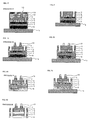
Figure 1] Figure 1 is a cross-sectional view of a thin film compound solar cell according to the present invention when a cell main body made of a plurality of compound semiconductor layers is formed. - [
Figure 2] Figure 2 is a cross-sectional view of the thin film compound solar cell when a rear surface electrode is formed. - [
Figure 3] Figure 3 is a cross-sectional view of the thin film compound solar cell when a rear surface film is formed. - [
Figure 4] Figure 4 is a cross-sectional view of the thin film compound solar cell when a reinforcing material is attached. - [
Figure 5] Figure 5 is a cross-sectional view of the thin film compound solar cell when a substrate is removed. - [
Figure 6] Figure 6 is a cross-sectional view of the thin film compound solar cell when an etching-stop layer is removed. - [
Figure 7] Figure 7 is a cross-sectional view of the thin film compound solar cell when a first protective film is formed. - [
Figure 8] Figure 8 is a cross-sectional view of the thin film compound solar cell when the protective film is patterned. - [
Figure 9] Figure 9 is a cross-sectional view of the thin film compound solar cell when a contact layer is etched. - [
Figure 10] Figure 10 is a cross-sectional view of the thin film compound solar cell when the protective film is separated. - [
Figure 11] Figure 11 is a cross-sectional view of the thin film compound solar cell when a second protective film is formed. - [
Figure 12] Figure 12 is a cross-sectional view of the thin film compound solar cell when the protective film is patterned. - [
Figure 13] Figure 13 is a cross-sectional view of the thin film compound solar cell at the time of mesa-etching. - [
Figure 14] Figure 14 is a cross-sectional view of the thin film compound solar cell when the protective film is separated. - [
Figure 15] Figure 15 is a cross-sectional view of the thin film compound solar cell when a third protective film formed. - [
Figure 16] Figure 16 is a cross-sectional view of the thin film compound solar cell at the time of patterning for forming a surface electrode. - [
Figure 17] Figure 17 is a cross-sectional view of the thin film compound solar cell when the surface electrode is formed. - [
Figure 18] Figure 18 is a cross-sectional view of the thin film compound solar cell when the protective film is removed. - [
Figure 19] Figure 19 is a cross-sectional view of the thin film compound solar cell when the reinforcing material is separated. - [
Figure 20] Figure 20 is a cross-sectional view of the thin film compound semiconductor solar cell when the cell is divided into solar cell elements. - [
Figure 21] Figure 21 is a cross-sectional view of a thin film compound solar cell when mesa-etching is performed before the contact layer etching in another manufacturing method. - [
Figure 22] Figure 22 is a cross-sectional view of the thin film compound solar cell when the surface electrode is formed in another manufacturing method. - [
Figure 23] Figure 23 is a cross-sectional view of the thin film compound solar cell when the contact layer is etched in another manufacturing method. - [
Figure 24] Figure 24 is a cross-sectional view of the thin film compound solar cell when a cell main body is formed in a conventional manufacturing method. - [
Figure 25] Figure 25 is a cross-sectional view of the thin film compound solar cell when a contact layer is etched. - [
Figure 26] Figure 26 is a cross-sectional view of the thin film compound solar cell when a surface electrode is formed. - [
Figure 27] Figure 27 is a cross-sectional view of the thin film compound solar cell when the cell is separated into solar cell elements. - [
Figure 28] Figure 28 is a cross-sectional view of the thin film compound solar cell when a surface film is formed. - [
Figure 29] Figure 29 is a cross-sectional view of the thin film compound solar cell when a reinforcing material is attached. - [
Figure 30] Figure 30 is a cross-sectional view of the thin film compound solar cell when a substrate is removed. - [
Figure 31] Figure 31 is a cross-sectional view of the thin film compound solar cell when a rear surface electrode is formed. - [
Figure 32] Figure 32 is a cross-sectional view of the thin film compound solar cell when the reinforcing material is separated. -
- 1
- substrate
- 2
- etching-stop layer
- 3
- contact layer
- 4
- emitter layer
- 5
- base layer
- 6
- buffer layer
- 7
- rear surface electrode
- 8
- rear surface film
- 9
- reinforcing material
- 10
- first protective film
- 11
- second protective film
- 12
- third protective film
- 13
- surface electrode
- A thin film compound solar cell according to the present embodiment has a structure including: a cell main body in which at least one PN junction is formed by laminating a plurality of compound semiconductor layers, each having a different chemical composition; a surface electrode which is formed on the light receiving surface of the cell main body; a rear surface electrode which is formed on the opposite surface of the cell main body; and a base material for the thin film solar cell. The base material is formed on the opposite surface of the cell main body, and the rear surface electrode is sandwiched between the cell main body and the base material.
- A method for manufacturing the solar cell having this structure will be described. In
process 1 shown inFigure 1 , a compound semiconductor layer made of single crystal thin films is formed by laminating, on asubstrate 1, an etching-stop layer 2 for suppressing infiltration of an etching solution from the side of the substrate, acontact layer 3, anemitter layer 4 made of a first compound semiconductor, abase layer 5 forming a PN junction with theemitter layer 4, and abuffer layer 6 in this order. Thesubstrate 1 has, for example, a wafer-like form, and a cell main body is formed by laminating, on thesubstrate 1, compound semiconductor layers, such as the etching-stop layer 2, thecontact layer 3, theemitter layer 4, thebase layer 5, and thebuffer layer 6, by a known process, for example, the epitaxial growth method described inPatent Document 1. - As the
substrate 1, it is possible to use a wafer made of a material, such as Ge, GaP, and GaAs. As the compound semiconductor layers, for example, the etching-stop layer 2 such as an InGaP layer, thecontact layer 3 such as an AlInP layer, theemitter layer 4 such as an N-type InGaP layer, thebase layer 5 such as a P-type InGaP layer, and thebuffer layer 6 such as an AlInP layer are used. - Note that the cell main body is assumed to have the 5 layer structure, but the layer structure of the cell main body is not limited to this. The cell main body may have, for example, a four layer structure, a six layer structure, or the like. Further, other than the etching-
stop layer 2, thecontact layer 3, theemitter layer 4, thebase layer 5, and thebuffer layer 6, the cell main body may include compound semiconductor layers, such as a BSF (back surface field) layer, a window layer, a tunnel junction layer of a multi-junction type solar cell, and the other emitter layer and the other base layer of the multi-junction type solar cell. - That is, it is only necessary that the cell main body formed on the
substrate 1 is made of a plurality of compound semiconductor layers, each having a different chemical composition, and that at least one PN junction is formed by the plurality of compound semiconductor layers. Further, it is only necessary that the plurality of compound semiconductor layers include at least a layer which is easily etched by a second etching solution for etching the contact layer and which is hardly etched by a third etching solution for mesa-etching, and a layer which is hardly etched by the second etching solution and which is easily etched by the third etching solution. The former layer is thecontact layer 3, and the latter layers are theemitter layer 4 and thebase layer 5. - In
process 2 shown inFigure 2 , arear surface electrode 7 is formed on the surface of thebuffer layer 6 which is the outermost surface of the compound semiconductor layers (the etching-stop layer 2, thecontact layer 3, theemitter layer 4, thebase layer 5, and the buffer layer 6) laminated onto each other. Therear surface electrode 7 is formed all over the compound semiconductor layer. Therear surface electrode 7 is formed by a method in which a metal paste made of Al, Ag, or the like, is applied to the outermost surface of the cell main body by screen printing. After the formation of therear surface electrode 7, the cell main body is subjected to heat treatment, so that therear surface electrode 7 is annealed. Therefore, the contact resistance between the surface of the compound semiconductor layer and therear surface electrode 7 can be reduced, and the adhesive force between the surface of the compound semiconductor layer and therear surface electrode 7 can be increased. - In
process 3 shown inFigure 3 , after the formation of therear surface electrode 7, a highly heat-resistantrear surface film 8 is formed on therear surface electrode 7. Therear surface film 8 is made of a material having heat resistance capable of withstanding a temperature of 300°C or more, and, for example, polyimide is used as the material of therear surface film 8. The method for forming therear surface film 8 includes a method in which a varnish-like resin is applied on therear surface electrode 7 at a normal temperature by a spin-coating method, or the like, and then annealed. - When the
rear surface film 8 is formed by applying and annealing a varnish of polyimide, it is necessary to control the film thickness of polyimide. This is because, when the film thickness of polyimide is 20 µm or more, air bubbles are mixed into the polyimide film, so as to prevent a flat film from being annealed, and because the amount of warpage of the polyimide film is also large, so as to damage the cell main body. When the film thickness of polyimide is reduced, the mixing of air bubbles is prevented in the thickness range of 20 µm or less, and the warpage of the polyimide film is also reduced. When the film thickness of polyimide is about 7 µm, the amount of warpage of the polyimide film is minimized. When the film thickness of polyimide is less than about 7 µm, the direction of warpage is reversed, and the amount of warpage is again increased. Therefore, as a result of consideration of the warpage amount of polyimide, and of the elasticity of polyimide as the base material of the cell main body, the film thickness of polyimide in the range of 5 to 15 µm is suitable for the production of the cell main body, and in particular the film thickness of about 7 µm is optimum. Note that, in the above, the method, in which the film is formed by annealing the varnish-like polyimide, is exemplified. However, besides this method, there is a method in which a thermal fusion adhesive film is used and press-fitted to therear surface electrode 7 while being heated. Thereby, therear surface film 8 is formed as the base material of the thin film solar cell so as to serve as the supporting body. Further, when the film thickness of the rear surface film is set to 15 µm or less, the base material with a less warpage amount can be formed, so that the warpage of the cell main body is controlled to reduce the warpage of the cell main body. - In
process 4 shown inFigure 4 , after the formation of therear surface film 8, a reinforcingmaterial 9 for reinforcing the compound semiconductor layer is bonded onto therear surface film 8. As the reinforcingmaterial 9, it is preferred to use a PET film, and the like, with an adhesive material whose adhesive force is lowered by irradiation of UV light. Thereby, the reinforcingmaterial 9 can be directly attached to therear surface film 8. - In
process 5 shown inFigure 5 , after the bonding of the reinforcingmaterial 9, thesubstrate 1 is etched and removed by using a first etching solution. As the first etching solution, a proper solution is selectively used according to the material of the substrate. In the case where the substrate is made of Ge, it is preferred to use a solution having a composition of hydrofluoric acid : aqueous hydrogen peroxide : water = 1:1:4. The etching-stop layer 2 is a layer which is hardly etched by the first etching solution. Thus, when the substrate is etched so that the etching-stop layer 2 is exposed, the progress of etching is stopped. Thereby, only thesubstrate 1 can be separated so that only the compound semiconductor layer is left. - In
process 6 shown inFigure 6 , after the etching of the substrate, the etching-stop layer 2 is removed by being etched by the second etching solution. Thecontact layer 3 is exposed at the outermost surface. - In
process 7 shown inFigure 7 , a firstprotective film 10 is applied and formed on thecontact layer 3 in order to protect the outermost surface of the cell main body from the chemical treatment (contact layer etching). Theprotective film 10 has resistance against the second etching solution used to etch the compound semiconductor layer in the subsequent process. When a photoresist is used as theprotective film 10, the processing is easily and surely performed. - In
process 8 shown inFigure 8 , after the formation of theprotective film 10, the patterning of theprotective film 10 for forming a surface electrode is performed by using a glass mask, so that an opening section is formed in theprotective film 10. Theprotective film 10 serves as an etching mask when the contact layer is etched in the subsequent process. - In
process 9 shown inFigure 9 , after theprotective film 10 is patterned, the contact layer is etched. The cell main body is immersed in the second etching solution capable of etching the compound semiconductor layer, so that thecontact layer 3 is etched by using the patternedprotective film 10 as an etching mask. An alkali solution is used as the second etching solution. A part of theemitter layer 4 is exposed at the outermost surface. - In
process 10 shown inFigure 10 , after the etching of thecontact layer 3, theprotective film 10 used as the etching mask for etching the contact layer is separated by a lift-off method. - In
process 11 shown inFigure 11 , a secondprotective film 11 is applied and formed in order to protect the outermost surface of the cell main body from mesa-etching. A photoresist is used as the secondprotective film 11. - In
process 12 shown inFigure 12 , after the formation of theprotective film 11, an opening section for defining the region of a solar cell element is formed in theprotective film 11 by patterning theprotective film 11 by using a glass mask. Theprotective film 11 serves as an etching mask at the time of mesa-etching in the subsequent process. - In
process 13 shown inFigure 13 , after the patterning of theprotective film 11, the cell main body is immersed in the third etching solution capable of etching the compound semiconductor layer, so that the cell main body is mesa-etched by using the patternedprotective film 11 as an etching mask. Theemitter layer 4 and thebase layer 5 are etched along the patternedprotective film 11. An alkali solution and an acid solution are used as the third etching solution. The region of the solar cell element can be defined by the mesa-etching. - In
process 14 shown inFigure 14 , after the mesa-etching, theprotective film 11 used as the etching mask is separated by the lift-off method. - In
process 15 shown inFigure 15 , a thirdprotective film 12 made of a photoresist is applied and formed on the whole outer surface of the etched cell main body in order to perform the patterning of the surface electrode. - In
process 16 shown inFigure 16 , after the formation of theprotective film 12, theprotective film 12 is patterned by using a glass mask, and thereby an opening section is formed in theprotective film 12 so that the patterning of the surface electrode can be performed. At this time, the patterning of theprotective film 12 is performed so that the opening section is formed on thecontact layer 3 patterned by the preceding process. - In
process 17 shown inFigure 17 , after the patterning of theprotective film 12, the cell main body, to which the reinforcingmaterial 9 is attached, is set in an electrode forming apparatus. Asurface electrode 13 is formed on theprotective film 12 and in the opening section of theprotective film 12. Thesurface electrode 13 is formed by applying an electrode material, such as Al or Ag, to the outermost surface of the cell main body by screen printing, or by vapor-depositing the electrode material on the outermost surface. - In
process 18 shown inFigure 18 , the cell main body, on which the electrode material laminated, is immersed in an organic solvent, such as acetone. The photoresist, which is theprotective film 12, is dissolved in the organic solvent, so that the electrode material attached on the photoresist is removed together with the photoresist. The electrode material is selectively attached only in the opening section, and thereby thesurface electrode 13 is formed on thecontact layer 3, so that the thin film compound semiconductor solar cell is formed. - In
process 19 shown inFigure 19 , after the formation of thesurface electrode 13, the thin film compound semiconductor solar cell is separated from the reinforcingmaterial 9. As the separation method, when the UV separation type material is used as the adhesive material, a method is used, in which the reinforcingmaterial 9 is separated from the cell main body by irradiating UV light by using a UV irradiation apparatus. - In
process 20 shown inFigure 20 , after the separation of the reinforcingmaterial 9, thesurface electrode 13 is annealed. By performing the heat treatment, it is possible to reduce the contact resistance between thecontact layer 3 and thesurface electrode 13, and to improve the adhesive property between thecontact layer 3 and thesurface electrode 13. Next, the thin film compound solar cell formed in the wafer is separated into a plurality of solar cell elements. As the separation method, a method is used, in which the thin film compound solar cell is fixed to a stage by vacuum suction, or the like, and in which the opening section formed by the mesa-etching is cut by a scriber so that the plurality of solar cell elements are formed. - Finally, a metallic ribbon made of Ag, or the like, for establishing electrical connection between the respective elements, is connected by welding, or the like, to an electrode pad on the electrode of each of the solar cell elements.
- In the thin film compound solar cell manufactured by the manufacturing method as described above, the reinforcing
material 9 is directly bonded to therear surface film 8 as the base material without using an adhesive, such as wax. Thereby, a solvent for separating the reinforcingmaterial 9 need not be used, so that it is possible to prevent the problem that therear surface film 8 is separated by the solvent. Therear surface film 8 has heat resistance capable of withstanding a temperature higher than the annealing temperature of thesurface electrode 13, and hence it is possible to anneal thesurface electrode 13 after therear surface film 8 is formed on therear surface electrode 7. - When the
surface electrode 13 and therear surface electrode 7 are annealed, the adhesive property of the electrodes with the cell main body is improved, so as to prevent each of the electrodes from being separated. Further, the contact resistance between the electrodes and the compound semiconductor layer can be reduced, so that the conversion efficiency is increased. - Further, the structure, in which the
surface electrode 13 is not covered with a surface film, is adopted, and hence thesurface electrode 13 is exposed. Thus, after thesubstrate 1 is removed, the metallic ribbon can be connected, and hence it is not necessary that, as in the conventional case, the metallic ribbon is protected when the substrate is removed. As a result, the number of processes can be reduced. - Further, a highly heat-resistant film, such as polyimide, is used as the base material, and thereby the film itself serves as a supporting body. Therefore, even when an external force is applied, the photovoltaic cell is prevented from being broken. Further, since the amount of warpage of the photovoltaic cell is changed according to the thickness of the film, the warpage of the cell can be reduced in such a manner that, when the film is formed, the thickness of the film is adjusted over the whole cell according to the thickness of the cell.
- Note that the present invention is not limited to the above described embodiment, but numerous modifications and changes can be obviously made therein without departing from the spirit and scope of the present invention. In another method for manufacturing a thin film compound solar cell, after
process 4 described above, thesubstrate 1 is separated from the cell main body, and the etching-stop layer 2 is removed. Then, the cell main body is mesa-etched as shown inFigure 21 . A protective film made of a photoresist is formed on thecontact layer 3, and the patterning for forming the surface electrode is performed. An electrode material is laminated on the protective film and on thecontact layer 3 in the opening section. When the protective film is removed, thesurface electrode 13 is formed as shown inFigure 22 . - Thereafter, as shown in
Figure 23 , thecontact layer 3 is etched by the contact layer etching. At this time, thesurface electrode 13 is used as an etching mask. Subsequently, the reinforcingmaterial 9 is separated from the cell main body, and thesurface electrode 13 is annealed. Then, the thin film compound solar cell is separated into a plurality of solar cell elements, and the metallic ribbon is finally connected to each of the solar cell elements. - With this manufacturing method, the
surface electrode 13 serves as a protective film in the contact layer etching. Thus, as compared with the above-described manufacturing method, the process of forming the protective film used to perform the contact layer etching can be eliminated, and hence the number of processes can be reduced. - Further, in another method for manufacturing the rear surface film which is the base material, the rear surface film is formed by applying and sintering a solution of polyamic acid which is a polyimide precursor. That is, a solution of varnish-like polyamic acid is applied on the rear surface electrode, and is annealed stepwise so that a polyimide film is formed.
- Specifically, the polyamic acid solution is applied on the rear surface electrode by a spin-coating method, or the like. Thereafter, when annealing is first performed at 120°C for one hour, the solvent of polyamic acid is evaporated, and the solution is temporarily cured. Then, the annealing temperature is increased stepwise. Finally, the annealing temperature is increased to the temperature at which the polyamic acid is polymerized and changed to a polyimide film. By this main curing, the polyimide film is formed.
- The reason for performing the annealing stepwise in this way is that, when the annealing is performed from the beginning at a temperature at which the polyamic acid starts to be polymerized, the surface layer of the polyamic acid solution is cured prior to the curing in the inside of the polyamic acid solution, with the result that an air bubble included in the solution at the time of annealing is left in the inside of the polyamic acid solution, and that the air bubble left in the inside of the polyamic acid solution is expanded to form a portion at which the rear surface electrode is not in close contact with the polyimide film. In addition, when the polyamic acid solution is rapidly cured, the contraction degree of the surface layer portion of the formed polyimide film becomes larger than the contraction degree in the inside of the polyimide film, so that the amount of warpage of the polyimide film is increased and thereby the photovoltaic cell is greatly warped. Thus, when the annealing temperature is increased stepwise as described above, the air bubble is prevented from being generated in the inside of the polyamic acid solution and the difference in the contraction degree between the surface layer portion and the inside of the polyimide film can also be prevented from occurring.
Claims (11)
- A method for manufacturing a thin film compound solar cell having a cell main body in which at least one PN junction is formed by a plurality of compound semiconductor layers, each having a different chemical composition, the method comprising: a process of forming a cell main body by forming an etching-stop layer for suppressing infiltration of an etching solution from the side of a substrate, a contact layer, an emitter layer made of a first conductivity type compound semiconductor, a base layer forming a PN junction with the emitter layer, and a buffer layer; a process of forming a rear surface electrode on the surface on the side of the compound semiconductor; a process of annealing the rear surface electrode; a process of forming a base material on the rear surface electrode; a process of attaching a reinforcing material on the base material; a process of separating the substrate from the cell main body; a process of forming a surface electrode on the exposed surface of the separated cell main body; a process of separating the reinforcing material; and a process of annealing the surface electrode.
- The method for manufacturing the thin film compound solar cell according to claim 1, further comprising: a process of, after the annealing of the surface electrode, separating the thin film compound solar cell into a plurality of solar cell elements; and a process of connecting a metallic ribbon to each electrode of the solar cell elements.
- The method for manufacturing the thin film compound solar cell according to one of claim 1 and claim 2, wherein the cell main body includes the etching-stop layer and the contact layer, the layers being laminated on the side of the substrate, the method further comprising: a process of, after the separation of the substrate, removing the etching-stop layer from the cell main body; a process of etching the contact layer into a predetermined pattern; and a process of mesa-etching the cell main body, wherein the surface electrode is formed on the mesa-etched contact layer.
- The method for manufacturing the thin film compound solar cell according to one of claim 1 and claim 2, wherein the cell main body includes the etching-stop layer and the contact layer, the layers being laminated on the side of the substrate, the method further comprising: a process of, after the separation of the substrate, removing the etching-stop layer from the cell main body; a process of mesa-etching the cell main body; and a process of, after the surface electrode is formed on the contact layer, etching the contact layer.
- The method for manufacturing the thin film compound solar cell according to one of claim 1 to claim 4, wherein the base material is made of a material having heat resistance capable of withstanding a temperature equal to or higher than the annealing temperature of the surface electrode.
- The method for manufacturing the thin film compound solar cell according to claim 5, wherein the base material is made of a film-like polyimide.
- The method for manufacturing the thin film compound solar cell according to claim 6, wherein the polyimide film is formed by applying and annealing a resinous polyimide.
- The method for manufacturing the thin film compound solar cell according to claim 6, wherein the polyimide film is formed by applying and annealing a solution of polyamic acid which is a polyimide precursor.
- The method for manufacturing the thin film compound solar cell according to one of claim 6 to claim 8, wherein the thickness of the polyimide film is set to 15 µm or less.
- A thin film compound solar cell comprising: a compound semiconductor layer in which at least one PN junction is formed; a surface electrode formed on one surface of the compound semiconductor layer; a polyimide film formed on the other surface of the compound semiconductor layer; and a rear surface electrode sandwiched between the compound semiconductor layer and the polyimide film.
- The thin film compound solar cell according to claim 10, wherein the compound semiconductor layer is made of an epitaxially grown single crystal thin film.
Applications Claiming Priority (2)
| Application Number | Priority Date | Filing Date | Title |
|---|---|---|---|
| JP2009044415 | 2009-02-26 | ||
| PCT/JP2010/052655 WO2010098293A1 (en) | 2009-02-26 | 2010-02-22 | Method for manufacturing thin film compound solar cell |
Publications (3)
| Publication Number | Publication Date |
|---|---|
| EP2403003A1 true EP2403003A1 (en) | 2012-01-04 |
| EP2403003A4 EP2403003A4 (en) | 2013-06-05 |
| EP2403003B1 EP2403003B1 (en) | 2018-10-03 |
Family
ID=42665500
Family Applications (1)
| Application Number | Title | Priority Date | Filing Date |
|---|---|---|---|
| EP10746174.1A Not-in-force EP2403003B1 (en) | 2009-02-26 | 2010-02-22 | Method for manufacturing thin film compound solar cell |
Country Status (4)
| Country | Link |
|---|---|
| US (2) | US20110303281A1 (en) |
| EP (1) | EP2403003B1 (en) |
| JP (1) | JP5554772B2 (en) |
| WO (1) | WO2010098293A1 (en) |
Families Citing this family (10)
| Publication number | Priority date | Publication date | Assignee | Title |
|---|---|---|---|---|
| US8912617B2 (en) * | 2011-10-27 | 2014-12-16 | Solar Junction Corporation | Method for making semiconductor light detection devices |
| US9263611B2 (en) | 2011-11-17 | 2016-02-16 | Solar Junction Corporation | Method for etching multi-layer epitaxial material |
| JP5840544B2 (en) * | 2012-03-21 | 2016-01-06 | シャープ株式会社 | Thin film compound solar cell and manufacturing method thereof |
| WO2014002824A1 (en) * | 2012-06-26 | 2014-01-03 | シャープ株式会社 | Thin film solar cell and method for producing same |
| JP2014017366A (en) * | 2012-07-09 | 2014-01-30 | Sharp Corp | Thin film compound solar battery cell and manufacturing method of the same |
| US9142615B2 (en) | 2012-10-10 | 2015-09-22 | Solar Junction Corporation | Methods and apparatus for identifying and reducing semiconductor failures |
| CN108140679A (en) * | 2015-09-28 | 2018-06-08 | 夏普株式会社 | Film compound solar cell, the manufacturing method of film compound solar cell, the manufacturing method of film compound solar cell array and film compound solar cell array |
| JP2019057536A (en) * | 2017-09-19 | 2019-04-11 | 株式会社東芝 | Solar cell, multi-junction type solar cell, solar cell module and photovoltaic power generation system |
| JP6834007B2 (en) | 2018-01-29 | 2021-02-24 | 株式会社東芝 | Solar cells, multi-junction solar cells, solar cell modules and photovoltaic power generation systems |
| CN112349796A (en) * | 2019-08-06 | 2021-02-09 | 东泰高科装备科技有限公司 | Gallium arsenide battery and preparation method thereof |
Family Cites Families (20)
| Publication number | Priority date | Publication date | Assignee | Title |
|---|---|---|---|---|
| US4370510A (en) * | 1980-09-26 | 1983-01-25 | California Institute Of Technology | Gallium arsenide single crystal solar cell structure and method of making |
| US4392297A (en) * | 1980-11-20 | 1983-07-12 | Spire Corporation | Process of making thin film high efficiency solar cells |
| US4514579A (en) * | 1984-01-30 | 1985-04-30 | Energy Conversion Devices, Inc. | Large area photovoltaic cell and method for producing same |
| US4681654A (en) * | 1986-05-21 | 1987-07-21 | International Business Machines Corporation | Flexible film semiconductor chip carrier |
| US5538902A (en) * | 1993-06-29 | 1996-07-23 | Sanyo Electric Co., Ltd. | Method of fabricating a photovoltaic device having a three-dimensional shape |
| JPH08107281A (en) * | 1994-10-06 | 1996-04-23 | Sumitomo Bakelite Co Ltd | Multilayer flexible printed circuit board and its manufacture |
| EP0849788B1 (en) * | 1996-12-18 | 2004-03-10 | Canon Kabushiki Kaisha | Process for producing semiconductor article by making use of a substrate having a porous semiconductor layer |
| ES2149137B1 (en) * | 1999-06-09 | 2001-11-16 | Univ Madrid Politecnica | SOLAR PHOTOVOLTAIC SEMICONDUCTOR CELL OF INTERMEDIATE CELL. |
| US6410362B1 (en) * | 2000-08-28 | 2002-06-25 | The Aerospace Corporation | Flexible thin film solar cell |
| JP2002289884A (en) * | 2001-03-27 | 2002-10-04 | Sumitomo Electric Ind Ltd | Solar cell, solar cell device |
| US8067687B2 (en) * | 2002-05-21 | 2011-11-29 | Alliance For Sustainable Energy, Llc | High-efficiency, monolithic, multi-bandgap, tandem photovoltaic energy converters |
| JP4471584B2 (en) | 2003-04-28 | 2010-06-02 | シャープ株式会社 | Method for producing compound solar cell |
| JP2007317834A (en) * | 2006-05-25 | 2007-12-06 | Toyobo Co Ltd | Film-like solar cell |
| US8536445B2 (en) * | 2006-06-02 | 2013-09-17 | Emcore Solar Power, Inc. | Inverted metamorphic multijunction solar cells |
| US20080245409A1 (en) * | 2006-12-27 | 2008-10-09 | Emcore Corporation | Inverted Metamorphic Solar Cell Mounted on Flexible Film |
| US20080223436A1 (en) * | 2007-03-15 | 2008-09-18 | Guardian Industries Corp. | Back reflector for use in photovoltaic device |
| JP5257918B2 (en) * | 2007-04-23 | 2013-08-07 | シャープ株式会社 | Compound semiconductor solar cell |
| US20090020149A1 (en) * | 2007-07-16 | 2009-01-22 | Woods Lawrence M | Hybrid Multi-Junction Photovoltaic Cells And Associated Methods |
| US20090038679A1 (en) * | 2007-08-09 | 2009-02-12 | Emcore Corporation | Thin Multijunction Solar Cells With Plated Metal OHMIC Contact and Support |
| US20100200063A1 (en) * | 2009-02-12 | 2010-08-12 | Derek Djeu | Thin film solar cell |
-
2010
- 2010-02-22 US US13/202,678 patent/US20110303281A1/en not_active Abandoned
- 2010-02-22 WO PCT/JP2010/052655 patent/WO2010098293A1/en not_active Ceased
- 2010-02-22 EP EP10746174.1A patent/EP2403003B1/en not_active Not-in-force
- 2010-02-22 JP JP2011501582A patent/JP5554772B2/en not_active Expired - Fee Related
-
2013
- 2013-10-23 US US14/060,985 patent/US9070819B2/en not_active Expired - Fee Related
Also Published As
| Publication number | Publication date |
|---|---|
| WO2010098293A1 (en) | 2010-09-02 |
| JPWO2010098293A1 (en) | 2012-08-30 |
| EP2403003B1 (en) | 2018-10-03 |
| JP5554772B2 (en) | 2014-07-23 |
| US9070819B2 (en) | 2015-06-30 |
| US20140051205A1 (en) | 2014-02-20 |
| US20110303281A1 (en) | 2011-12-15 |
| EP2403003A4 (en) | 2013-06-05 |
Similar Documents
| Publication | Publication Date | Title |
|---|---|---|
| US9070819B2 (en) | Method for manufacturing thin film compound solar cell | |
| US6184056B1 (en) | Process for producing solar cells and solar cells produced thereby | |
| US10424689B2 (en) | Method of manufacturing solar battery | |
| US8173895B2 (en) | Solar cell | |
| EP2413380A1 (en) | Back electrode type solar cell, wiring sheet, solar cell provided with wiring sheet, solar cell module, method for manufacturing solar cell provided with wiring sheet, and method for manufacturing solar cell module | |
| CN110047946A (en) | The metal foil of thin silicon solar battery assists manufacture | |
| JP5232466B2 (en) | Photovoltaic device | |
| CN100490183C (en) | Solar battery unit and its making method | |
| CN101432888B (en) | Ultra lightweight photovoltaic device and method for its manufacture | |
| CN102804405A (en) | Method of manufacturing a photovoltaic module comprising a back contact cell | |
| JP2010157553A (en) | Interconnect sheet, solar cell with the interconnect cell, solar cell module, and method of manufacturing the solar cell with the interconnect sheet, and method of manufacturing the solar cell moidule | |
| JPH114008A (en) | Manufacturing method of thin film solar cell | |
| JP2014017366A (en) | Thin film compound solar battery cell and manufacturing method of the same | |
| CN110603649A (en) | Photoelectric conversion device and solar cell module provided with same | |
| JP5980923B2 (en) | Thin film solar cell and manufacturing method thereof | |
| CN114447155B (en) | Method for manufacturing gate electrode of flexible solar cell and semiconductor device | |
| JP4762753B2 (en) | Method for producing thin film single crystal compound solar cell | |
| EP4391018A1 (en) | Provisionally bonded wafer and method for producing same | |
| JP4753816B2 (en) | Solar cell and manufacturing method thereof | |
| JP3766248B2 (en) | Manufacturing method of solar cell module | |
| CN106783716B (en) | Method for reducing breakage rate of fragile substrate in semiconductor manufacturing process | |
| JP2006041209A (en) | Semiconductor device manufacturing method and semiconductor device manufactured thereby | |
| HK1148608A (en) | Solar cell | |
| HK1111807B (en) | Solar cell | |
| JP2014053422A (en) | Photoelectric conversion device |
Legal Events
| Date | Code | Title | Description |
|---|---|---|---|
| PUAI | Public reference made under article 153(3) epc to a published international application that has entered the european phase |
Free format text: ORIGINAL CODE: 0009012 |
|
| 17P | Request for examination filed |
Effective date: 20110819 |
|
| AK | Designated contracting states |
Kind code of ref document: A1 Designated state(s): AT BE BG CH CY CZ DE DK EE ES FI FR GB GR HR HU IE IS IT LI LT LU LV MC MK MT NL NO PL PT RO SE SI SK SM TR |
|
| DAX | Request for extension of the european patent (deleted) | ||
| A4 | Supplementary search report drawn up and despatched |
Effective date: 20130506 |
|
| RIC1 | Information provided on ipc code assigned before grant |
Ipc: H01L 31/04 20060101AFI20130426BHEP Ipc: H01L 31/048 20060101ALI20130426BHEP Ipc: H01L 31/0687 20120101ALI20130426BHEP Ipc: H01L 31/0693 20120101ALI20130426BHEP Ipc: H01L 31/18 20060101ALI20130426BHEP Ipc: H01L 31/0392 20060101ALI20130426BHEP |
|
| 17Q | First examination report despatched |
Effective date: 20151012 |
|
| REG | Reference to a national code |
Ref country code: DE Ref legal event code: R079 Ref document number: 602010054050 Country of ref document: DE Free format text: PREVIOUS MAIN CLASS: H01L0031040000 Ipc: H01L0031068700 |
|
| RIC1 | Information provided on ipc code assigned before grant |
Ipc: H01L 31/0224 20060101ALI20171011BHEP Ipc: H01L 31/0392 20060101ALI20171011BHEP Ipc: H01L 31/0687 20120101AFI20171011BHEP Ipc: H01L 31/18 20060101ALI20171011BHEP Ipc: H01L 31/0693 20120101ALI20171011BHEP |
|
| GRAP | Despatch of communication of intention to grant a patent |
Free format text: ORIGINAL CODE: EPIDOSNIGR1 |
|
| STAA | Information on the status of an ep patent application or granted ep patent |
Free format text: STATUS: GRANT OF PATENT IS INTENDED |
|
| INTG | Intention to grant announced |
Effective date: 20171213 |
|
| GRAJ | Information related to disapproval of communication of intention to grant by the applicant or resumption of examination proceedings by the epo deleted |
Free format text: ORIGINAL CODE: EPIDOSDIGR1 |
|
| STAA | Information on the status of an ep patent application or granted ep patent |
Free format text: STATUS: EXAMINATION IS IN PROGRESS |
|
| INTC | Intention to grant announced (deleted) | ||
| GRAP | Despatch of communication of intention to grant a patent |
Free format text: ORIGINAL CODE: EPIDOSNIGR1 |
|
| STAA | Information on the status of an ep patent application or granted ep patent |
Free format text: STATUS: GRANT OF PATENT IS INTENDED |
|
| INTG | Intention to grant announced |
Effective date: 20180426 |
|
| GRAS | Grant fee paid |
Free format text: ORIGINAL CODE: EPIDOSNIGR3 |
|
| GRAA | (expected) grant |
Free format text: ORIGINAL CODE: 0009210 |
|
| STAA | Information on the status of an ep patent application or granted ep patent |
Free format text: STATUS: THE PATENT HAS BEEN GRANTED |
|
| AK | Designated contracting states |
Kind code of ref document: B1 Designated state(s): AT BE BG CH CY CZ DE DK EE ES FI FR GB GR HR HU IE IS IT LI LT LU LV MC MK MT NL NO PL PT RO SE SI SK SM TR |
|
| REG | Reference to a national code |
Ref country code: GB Ref legal event code: FG4D |
|
| REG | Reference to a national code |
Ref country code: CH Ref legal event code: EP Ref country code: AT Ref legal event code: REF Ref document number: 1049561 Country of ref document: AT Kind code of ref document: T Effective date: 20181015 |
|
| REG | Reference to a national code |
Ref country code: IE Ref legal event code: FG4D Ref country code: DE Ref legal event code: R096 Ref document number: 602010054050 Country of ref document: DE |
|
| REG | Reference to a national code |
Ref country code: NL Ref legal event code: MP Effective date: 20181003 |
|
| REG | Reference to a national code |
Ref country code: LT Ref legal event code: MG4D |
|
| REG | Reference to a national code |
Ref country code: AT Ref legal event code: MK05 Ref document number: 1049561 Country of ref document: AT Kind code of ref document: T Effective date: 20181003 |
|
| PG25 | Lapsed in a contracting state [announced via postgrant information from national office to epo] |
Ref country code: NL Free format text: LAPSE BECAUSE OF FAILURE TO SUBMIT A TRANSLATION OF THE DESCRIPTION OR TO PAY THE FEE WITHIN THE PRESCRIBED TIME-LIMIT Effective date: 20181003 |
|
| PG25 | Lapsed in a contracting state [announced via postgrant information from national office to epo] |
Ref country code: ES Free format text: LAPSE BECAUSE OF FAILURE TO SUBMIT A TRANSLATION OF THE DESCRIPTION OR TO PAY THE FEE WITHIN THE PRESCRIBED TIME-LIMIT Effective date: 20181003 Ref country code: LV Free format text: LAPSE BECAUSE OF FAILURE TO SUBMIT A TRANSLATION OF THE DESCRIPTION OR TO PAY THE FEE WITHIN THE PRESCRIBED TIME-LIMIT Effective date: 20181003 Ref country code: AT Free format text: LAPSE BECAUSE OF FAILURE TO SUBMIT A TRANSLATION OF THE DESCRIPTION OR TO PAY THE FEE WITHIN THE PRESCRIBED TIME-LIMIT Effective date: 20181003 Ref country code: PL Free format text: LAPSE BECAUSE OF FAILURE TO SUBMIT A TRANSLATION OF THE DESCRIPTION OR TO PAY THE FEE WITHIN THE PRESCRIBED TIME-LIMIT Effective date: 20181003 Ref country code: LT Free format text: LAPSE BECAUSE OF FAILURE TO SUBMIT A TRANSLATION OF THE DESCRIPTION OR TO PAY THE FEE WITHIN THE PRESCRIBED TIME-LIMIT Effective date: 20181003 Ref country code: NO Free format text: LAPSE BECAUSE OF FAILURE TO SUBMIT A TRANSLATION OF THE DESCRIPTION OR TO PAY THE FEE WITHIN THE PRESCRIBED TIME-LIMIT Effective date: 20190103 Ref country code: CZ Free format text: LAPSE BECAUSE OF FAILURE TO SUBMIT A TRANSLATION OF THE DESCRIPTION OR TO PAY THE FEE WITHIN THE PRESCRIBED TIME-LIMIT Effective date: 20181003 Ref country code: FI Free format text: LAPSE BECAUSE OF FAILURE TO SUBMIT A TRANSLATION OF THE DESCRIPTION OR TO PAY THE FEE WITHIN THE PRESCRIBED TIME-LIMIT Effective date: 20181003 Ref country code: IS Free format text: LAPSE BECAUSE OF FAILURE TO SUBMIT A TRANSLATION OF THE DESCRIPTION OR TO PAY THE FEE WITHIN THE PRESCRIBED TIME-LIMIT Effective date: 20190203 Ref country code: BG Free format text: LAPSE BECAUSE OF FAILURE TO SUBMIT A TRANSLATION OF THE DESCRIPTION OR TO PAY THE FEE WITHIN THE PRESCRIBED TIME-LIMIT Effective date: 20190103 Ref country code: HR Free format text: LAPSE BECAUSE OF FAILURE TO SUBMIT A TRANSLATION OF THE DESCRIPTION OR TO PAY THE FEE WITHIN THE PRESCRIBED TIME-LIMIT Effective date: 20181003 |
|
| PGFP | Annual fee paid to national office [announced via postgrant information from national office to epo] |
Ref country code: DE Payment date: 20190219 Year of fee payment: 10 |
|
| PG25 | Lapsed in a contracting state [announced via postgrant information from national office to epo] |
Ref country code: GR Free format text: LAPSE BECAUSE OF FAILURE TO SUBMIT A TRANSLATION OF THE DESCRIPTION OR TO PAY THE FEE WITHIN THE PRESCRIBED TIME-LIMIT Effective date: 20190104 Ref country code: SE Free format text: LAPSE BECAUSE OF FAILURE TO SUBMIT A TRANSLATION OF THE DESCRIPTION OR TO PAY THE FEE WITHIN THE PRESCRIBED TIME-LIMIT Effective date: 20181003 Ref country code: PT Free format text: LAPSE BECAUSE OF FAILURE TO SUBMIT A TRANSLATION OF THE DESCRIPTION OR TO PAY THE FEE WITHIN THE PRESCRIBED TIME-LIMIT Effective date: 20190203 |
|
| REG | Reference to a national code |
Ref country code: DE Ref legal event code: R097 Ref document number: 602010054050 Country of ref document: DE |
|
| PG25 | Lapsed in a contracting state [announced via postgrant information from national office to epo] |
Ref country code: DK Free format text: LAPSE BECAUSE OF FAILURE TO SUBMIT A TRANSLATION OF THE DESCRIPTION OR TO PAY THE FEE WITHIN THE PRESCRIBED TIME-LIMIT Effective date: 20181003 Ref country code: IT Free format text: LAPSE BECAUSE OF FAILURE TO SUBMIT A TRANSLATION OF THE DESCRIPTION OR TO PAY THE FEE WITHIN THE PRESCRIBED TIME-LIMIT Effective date: 20181003 |
|
| PLBE | No opposition filed within time limit |
Free format text: ORIGINAL CODE: 0009261 |
|
| STAA | Information on the status of an ep patent application or granted ep patent |
Free format text: STATUS: NO OPPOSITION FILED WITHIN TIME LIMIT |
|
| PG25 | Lapsed in a contracting state [announced via postgrant information from national office to epo] |
Ref country code: RO Free format text: LAPSE BECAUSE OF FAILURE TO SUBMIT A TRANSLATION OF THE DESCRIPTION OR TO PAY THE FEE WITHIN THE PRESCRIBED TIME-LIMIT Effective date: 20181003 Ref country code: SK Free format text: LAPSE BECAUSE OF FAILURE TO SUBMIT A TRANSLATION OF THE DESCRIPTION OR TO PAY THE FEE WITHIN THE PRESCRIBED TIME-LIMIT Effective date: 20181003 Ref country code: EE Free format text: LAPSE BECAUSE OF FAILURE TO SUBMIT A TRANSLATION OF THE DESCRIPTION OR TO PAY THE FEE WITHIN THE PRESCRIBED TIME-LIMIT Effective date: 20181003 Ref country code: SM Free format text: LAPSE BECAUSE OF FAILURE TO SUBMIT A TRANSLATION OF THE DESCRIPTION OR TO PAY THE FEE WITHIN THE PRESCRIBED TIME-LIMIT Effective date: 20181003 |
|
| 26N | No opposition filed |
Effective date: 20190704 |
|
| REG | Reference to a national code |
Ref country code: CH Ref legal event code: PL |
|
| GBPC | Gb: european patent ceased through non-payment of renewal fee |
Effective date: 20190222 |
|
| PG25 | Lapsed in a contracting state [announced via postgrant information from national office to epo] |
Ref country code: SI Free format text: LAPSE BECAUSE OF FAILURE TO SUBMIT A TRANSLATION OF THE DESCRIPTION OR TO PAY THE FEE WITHIN THE PRESCRIBED TIME-LIMIT Effective date: 20181003 Ref country code: LU Free format text: LAPSE BECAUSE OF NON-PAYMENT OF DUE FEES Effective date: 20190222 Ref country code: MC Free format text: LAPSE BECAUSE OF FAILURE TO SUBMIT A TRANSLATION OF THE DESCRIPTION OR TO PAY THE FEE WITHIN THE PRESCRIBED TIME-LIMIT Effective date: 20181003 |
|
| REG | Reference to a national code |
Ref country code: BE Ref legal event code: MM Effective date: 20190228 |
|
| REG | Reference to a national code |
Ref country code: IE Ref legal event code: MM4A |
|
| PG25 | Lapsed in a contracting state [announced via postgrant information from national office to epo] |
Ref country code: CH Free format text: LAPSE BECAUSE OF NON-PAYMENT OF DUE FEES Effective date: 20190228 Ref country code: LI Free format text: LAPSE BECAUSE OF NON-PAYMENT OF DUE FEES Effective date: 20190228 |
|
| PG25 | Lapsed in a contracting state [announced via postgrant information from national office to epo] |
Ref country code: IE Free format text: LAPSE BECAUSE OF NON-PAYMENT OF DUE FEES Effective date: 20190222 Ref country code: GB Free format text: LAPSE BECAUSE OF NON-PAYMENT OF DUE FEES Effective date: 20190222 |
|
| PG25 | Lapsed in a contracting state [announced via postgrant information from national office to epo] |
Ref country code: BE Free format text: LAPSE BECAUSE OF NON-PAYMENT OF DUE FEES Effective date: 20190228 Ref country code: FR Free format text: LAPSE BECAUSE OF NON-PAYMENT OF DUE FEES Effective date: 20190228 |
|
| PG25 | Lapsed in a contracting state [announced via postgrant information from national office to epo] |
Ref country code: TR Free format text: LAPSE BECAUSE OF FAILURE TO SUBMIT A TRANSLATION OF THE DESCRIPTION OR TO PAY THE FEE WITHIN THE PRESCRIBED TIME-LIMIT Effective date: 20181003 |
|
| PG25 | Lapsed in a contracting state [announced via postgrant information from national office to epo] |
Ref country code: MT Free format text: LAPSE BECAUSE OF NON-PAYMENT OF DUE FEES Effective date: 20190222 |
|
| REG | Reference to a national code |
Ref country code: DE Ref legal event code: R119 Ref document number: 602010054050 Country of ref document: DE |
|
| PG25 | Lapsed in a contracting state [announced via postgrant information from national office to epo] |
Ref country code: DE Free format text: LAPSE BECAUSE OF NON-PAYMENT OF DUE FEES Effective date: 20200901 |
|
| PG25 | Lapsed in a contracting state [announced via postgrant information from national office to epo] |
Ref country code: CY Free format text: LAPSE BECAUSE OF FAILURE TO SUBMIT A TRANSLATION OF THE DESCRIPTION OR TO PAY THE FEE WITHIN THE PRESCRIBED TIME-LIMIT Effective date: 20181003 |
|
| PG25 | Lapsed in a contracting state [announced via postgrant information from national office to epo] |
Ref country code: HU Free format text: LAPSE BECAUSE OF FAILURE TO SUBMIT A TRANSLATION OF THE DESCRIPTION OR TO PAY THE FEE WITHIN THE PRESCRIBED TIME-LIMIT; INVALID AB INITIO Effective date: 20100222 |
|
| PG25 | Lapsed in a contracting state [announced via postgrant information from national office to epo] |
Ref country code: MK Free format text: LAPSE BECAUSE OF FAILURE TO SUBMIT A TRANSLATION OF THE DESCRIPTION OR TO PAY THE FEE WITHIN THE PRESCRIBED TIME-LIMIT Effective date: 20181003 |