EP2400821A1 - Wiring substrate - Google Patents
Wiring substrate Download PDFInfo
- Publication number
- EP2400821A1 EP2400821A1 EP11160730A EP11160730A EP2400821A1 EP 2400821 A1 EP2400821 A1 EP 2400821A1 EP 11160730 A EP11160730 A EP 11160730A EP 11160730 A EP11160730 A EP 11160730A EP 2400821 A1 EP2400821 A1 EP 2400821A1
- Authority
- EP
- European Patent Office
- Prior art keywords
- fiber bundles
- insulating layer
- glass fiber
- disposed
- wirings
- Prior art date
- Legal status (The legal status is an assumption and is not a legal conclusion. Google has not performed a legal analysis and makes no representation as to the accuracy of the status listed.)
- Withdrawn
Links
Images










Classifications
-
- H—ELECTRICITY
- H05—ELECTRIC TECHNIQUES NOT OTHERWISE PROVIDED FOR
- H05K—PRINTED CIRCUITS; CASINGS OR CONSTRUCTIONAL DETAILS OF ELECTRIC APPARATUS; MANUFACTURE OF ASSEMBLAGES OF ELECTRICAL COMPONENTS
- H05K1/00—Printed circuits
- H05K1/02—Details
- H05K1/0213—Electrical arrangements not otherwise provided for
- H05K1/0237—High frequency adaptations
- H05K1/0248—Skew reduction or using delay lines
-
- H—ELECTRICITY
- H05—ELECTRIC TECHNIQUES NOT OTHERWISE PROVIDED FOR
- H05K—PRINTED CIRCUITS; CASINGS OR CONSTRUCTIONAL DETAILS OF ELECTRIC APPARATUS; MANUFACTURE OF ASSEMBLAGES OF ELECTRICAL COMPONENTS
- H05K1/00—Printed circuits
- H05K1/02—Details
- H05K1/03—Use of materials for the substrate
- H05K1/0313—Organic insulating material
- H05K1/0353—Organic insulating material consisting of two or more materials, e.g. two or more polymers, polymer + filler, + reinforcement
- H05K1/0366—Organic insulating material consisting of two or more materials, e.g. two or more polymers, polymer + filler, + reinforcement reinforced, e.g. by fibres, fabrics
-
- H—ELECTRICITY
- H05—ELECTRIC TECHNIQUES NOT OTHERWISE PROVIDED FOR
- H05K—PRINTED CIRCUITS; CASINGS OR CONSTRUCTIONAL DETAILS OF ELECTRIC APPARATUS; MANUFACTURE OF ASSEMBLAGES OF ELECTRICAL COMPONENTS
- H05K1/00—Printed circuits
- H05K1/02—Details
- H05K1/0213—Electrical arrangements not otherwise provided for
- H05K1/0237—High frequency adaptations
- H05K1/024—Dielectric details, e.g. changing the dielectric material around a transmission line
-
- H—ELECTRICITY
- H05—ELECTRIC TECHNIQUES NOT OTHERWISE PROVIDED FOR
- H05K—PRINTED CIRCUITS; CASINGS OR CONSTRUCTIONAL DETAILS OF ELECTRIC APPARATUS; MANUFACTURE OF ASSEMBLAGES OF ELECTRICAL COMPONENTS
- H05K1/00—Printed circuits
- H05K1/02—Details
- H05K1/0213—Electrical arrangements not otherwise provided for
- H05K1/0237—High frequency adaptations
- H05K1/0245—Lay-out of balanced signal pairs, e.g. differential lines or twisted lines
-
- H—ELECTRICITY
- H05—ELECTRIC TECHNIQUES NOT OTHERWISE PROVIDED FOR
- H05K—PRINTED CIRCUITS; CASINGS OR CONSTRUCTIONAL DETAILS OF ELECTRIC APPARATUS; MANUFACTURE OF ASSEMBLAGES OF ELECTRICAL COMPONENTS
- H05K1/00—Printed circuits
- H05K1/02—Details
- H05K1/0266—Marks, test patterns or identification means
- H05K1/0269—Marks, test patterns or identification means for visual or optical inspection
-
- H—ELECTRICITY
- H05—ELECTRIC TECHNIQUES NOT OTHERWISE PROVIDED FOR
- H05K—PRINTED CIRCUITS; CASINGS OR CONSTRUCTIONAL DETAILS OF ELECTRIC APPARATUS; MANUFACTURE OF ASSEMBLAGES OF ELECTRICAL COMPONENTS
- H05K2201/00—Indexing scheme relating to printed circuits covered by H05K1/00
- H05K2201/02—Fillers; Particles; Fibers; Reinforcement materials
- H05K2201/0275—Fibers and reinforcement materials
- H05K2201/029—Woven fibrous reinforcement or textile
-
- H—ELECTRICITY
- H05—ELECTRIC TECHNIQUES NOT OTHERWISE PROVIDED FOR
- H05K—PRINTED CIRCUITS; CASINGS OR CONSTRUCTIONAL DETAILS OF ELECTRIC APPARATUS; MANUFACTURE OF ASSEMBLAGES OF ELECTRICAL COMPONENTS
- H05K2201/00—Indexing scheme relating to printed circuits covered by H05K1/00
- H05K2201/09—Shape and layout
- H05K2201/09209—Shape and layout details of conductors
- H05K2201/09218—Conductive traces
- H05K2201/09272—Layout details of angles or corners
-
- H—ELECTRICITY
- H05—ELECTRIC TECHNIQUES NOT OTHERWISE PROVIDED FOR
- H05K—PRINTED CIRCUITS; CASINGS OR CONSTRUCTIONAL DETAILS OF ELECTRIC APPARATUS; MANUFACTURE OF ASSEMBLAGES OF ELECTRICAL COMPONENTS
- H05K2203/00—Indexing scheme relating to apparatus or processes for manufacturing printed circuits covered by H05K3/00
- H05K2203/16—Inspection; Monitoring; Aligning
- H05K2203/166—Alignment or registration; Control of registration
-
- H—ELECTRICITY
- H05—ELECTRIC TECHNIQUES NOT OTHERWISE PROVIDED FOR
- H05K—PRINTED CIRCUITS; CASINGS OR CONSTRUCTIONAL DETAILS OF ELECTRIC APPARATUS; MANUFACTURE OF ASSEMBLAGES OF ELECTRICAL COMPONENTS
- H05K2203/00—Indexing scheme relating to apparatus or processes for manufacturing printed circuits covered by H05K3/00
- H05K2203/16—Inspection; Monitoring; Aligning
- H05K2203/167—Using mechanical means for positioning, alignment or registration, e.g. using rod-in-hole alignment
-
- Y—GENERAL TAGGING OF NEW TECHNOLOGICAL DEVELOPMENTS; GENERAL TAGGING OF CROSS-SECTIONAL TECHNOLOGIES SPANNING OVER SEVERAL SECTIONS OF THE IPC; TECHNICAL SUBJECTS COVERED BY FORMER USPC CROSS-REFERENCE ART COLLECTIONS [XRACs] AND DIGESTS
- Y10—TECHNICAL SUBJECTS COVERED BY FORMER USPC
- Y10T—TECHNICAL SUBJECTS COVERED BY FORMER US CLASSIFICATION
- Y10T29/00—Metal working
- Y10T29/49—Method of mechanical manufacture
- Y10T29/49002—Electrical device making
- Y10T29/49117—Conductor or circuit manufacturing
Definitions
- the embodiments discussed herein are related to a wiring substrate in which differential wirings are formed on an insulating layer.
- An object of a conventional technology is to avoid accumulation of phase shift on one of a P wiring and an N wiring, by arranging yarn of a glass cloth parallel to an extending direction of wirings so that the yarn intersects the differential wirings in a zig-zag manner, and to therefore prevent generation of skew between the wirings.
- Warp yarn 4 and weft yarn 5 constituting glass cloth used for forming a substrate for lamination are arranged so that one or both of the warp yarn 4 and the weft yarn 5 are arranged in a zig-zag manner by a length equal to the total of the widths of differential wirings and the distances between the wirings. Accordingly, the variation in the relative dielectric constant of the substrate for lamination is averaged, thus mitigating the deterioration of waveform quality in differential transmission.
- Patent document 1 Japanese Laid-Open Patent Publication No. 2009-73946
- a wiring substrate includes a pair of differential wirings; a first insulating layer that is provided adjacent to one side of the pair of differential wirings, the first insulating layer including first fiber bundles disposed in parallel to an extending direction of the pair of differential wirings; a second insulating layer that is provided adjacent to another side of the pair of differential wirings, the second insulating layer including second fiber bundles disposed in parallel to the extending direction of the pair of differential wirings, the second fiber bundles being disposed by the same pitch as the first fiber bundles; a third insulating layer that is provided on a side of the first insulating layer opposite to a side of the first insulating layer that is adjacent to the pair of differential wirings, the third insulating layer including third fiber bundles disposed in parallel to the extending direction of the pair of differential wirings; and a fourth insulating layer that is provided on a side of the second insulating layer opposite to a side of the second insulating layer that is adjacent to the pair of differential wirings; and a fourth
- a reference 170, an insulating layer 110A, wirings 150 and 160, an insulating layer 110B, and a reference 180 are laminated.
- the insulating layer 110A includes glass fiber bundles 120A and 130A, and insulating resin 140A.
- the glass fiber bundles 120A and 130A are impregnated with the insulating resin 140A.
- the insulating layer 110B includes glass fiber bundles 120B and 130B, and insulating resin 140B.
- the glass fiber bundles 120B and 130B are impregnated with the insulating resin 140B.
- the glass fiber bundles 120A are disposed in a direction parallel to an X axis, and the glass fiber bundles 130A are disposed in a direction parallel to a Y axis.
- the glass fiber bundles 120A and 130A are plain-woven in a lattice-like manner.
- the glass fiber bundles 120B are disposed in a direction parallel to an X axis, and the glass fiber bundles 130B are disposed in a direction parallel to a Y axis.
- the glass fiber bundles 120B and 130B are plain-woven in a lattice-like manner.
- the glass fiber bundles 120B and 130B are disposed at positions corresponding to the glass fiber bundles 120A and 130A.
- the wirings 150 and 160 are selectively formed on one side of the insulating layer 110A.
- the reference 170 is formed on substantially the entire surface of the other side of the insulating layer 110A.
- the reference 180 is formed on substantially the entire surface of the insulating layer 110B, on the side opposite to that adjacent to the wirings 150 and 160.
- the wirings 150 and 160 are conducting bodies through which predetermined electric signals flow.
- the references 170 and 180 are conducting bodies acting as return circuits of the predetermined electric signals flowing through the wirings 150 and 160.
- the wirings 150 and 160 are disposed in parallel, and are differential wirings used for the differential transmission method. Typically, high-speed transmission is performed with high performance by the differential transmission method. However, the wiring 150 is disposed on one of the glass fiber bundles 130A, while the wiring 160 is disposed between the glass fiber bundle 130A on which the wiring 150 is disposed and an adjacent glass fiber bundle 130A (between adjacent glass fiber bundles 130A).
- a wiring substrate includes wirings positioned on glass fiber bundles as well as wirings positioned between glass fiber bundles.
- the relative permittivity on a glass fiber bundle is different from the relative permittivity between glass fiber bundles (on the insulating resin), due to the difference in the glass fiber density. Therefore, when there are wirings positioned on glass fiber bundles as well as wirings positioned between glass fiber bundles, there may be inconsistencies in characteristic impedance and differences in the propagation delay time.
- the frequency of high-speed transmission has approached a range of 3 GHz through 5 GHz, and therefore problems are arising in connection with inconsistencies in characteristic impedance and differences in the propagation delay time.
- the technology of arranging wirings in a zig-zag manner uses excessive wirings, and therefore the manufacturing cost is increased. Furthermore, with the technology of propagating high frequency signals by using a low-dielectric material as the material of the wiring substrate, the low-dielectric material is expensive, and therefore the manufacturing cost is increased. Furthermore, with the technology of tilting the wiring substrate and laminating layers, the material efficiency significantly decreases as the tilt angle increases, and therefore the manufacturing cost is increased.
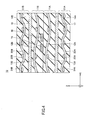
- FIG. 3 is a transparent plan view of main parts of a wiring substrate according to a first embodiment.
- FIG. 4 is a cross-sectional view of main parts of the wiring substrate according to the first embodiment. Some of the elements illustrated in FIG. 4 are not illustrated in FIG. 3 .
- FIG. 4 is a cross-sectional view cut along a line B-B in FIG. 3 .
- an insulating layer 21A, a reference 17, an insulating layer 11A, wirings 15 and 16, an insulating layer 11B, a reference 18, and an insulating layer 21B are laminated. A detailed description is given of the respective components of the wiring substrate 10.
- the insulating layer 11A includes glass fiber bundles 12A and 13A, and insulating resin 14A.
- the glass fiber bundles 12A and 13A are impregnated with the insulating resin 14A.
- the insulating resin 14A may be made of a material such as epoxy resin, polymide resin, and polyester resin.
- the insulating resin 14A may include filler such as silica and alumina.
- the glass fiber bundles 12A having a width of W 1 are disposed in a direction parallel to an X axis with intervals of S 1 .
- the glass fiber bundles 13A having a width of W 2 are disposed in a direction parallel to a Y axis with intervals of S 2 .
- the glass fiber bundles 12A and 13A are plain-woven in a lattice-like manner.
- a member in which glass fiber bundles are plain-woven in a lattice-like manner may be referred to as a glass cloth.
- Each of the glass fiber bundles 12A and 13A is formed by bundling together plural glass fibers of, for example, several millimeters to form a bundle of, for example, several hundred millimeters.
- At gap parts 12X (so-called basket holes) formed by the glass fiber bundles 12A and 13A no glass fiber is present; the gap parts 12X are filled with the insulating resin 14A.
- the insulating layer 11B includes glass fiber bundles 12B and 13B, and insulating resin 14B.
- the glass fiber bundles 12B and 13B are impregnated with the insulating resin 14B.
- the insulating resin 14B may be made of the same material as that of the insulating resin 14A, and is thus not further described.
- the glass fiber bundles 12B having a width of W 1 are disposed in a direction parallel to the X axis with intervals of S 1 .
- the glass fiber bundles 13B having a width of W 2 are disposed in a direction parallel to the Y axis with intervals of S 2 .
- the glass fiber bundles 12B and 13B are plain-woven in a lattice-like manner. Details of the glass fiber bundles 12B and 13B are the same as those of the glass fiber bundles 12A and 13A, and are thus not further described.
- the width W 1 may be equal to the width W 2
- the interval S 1 may be equal to the interval S 2 .
- the glass fiber bundles 12B and 13B are respectively disposed at positions corresponding to the glass fiber bundles 12A and 13A. That is to say, the glass fiber bundles 12B and 13B are respectively disposed at positions overlapping the glass fiber bundles 12A and 13A in a planar view.
- a planar view refers to viewing an object from a + direction to a - direction (or from a - direction to a + direction) of a Z axis in FIGS. 3 and 4 .
- the widths and intervals of the glass fiber bundles 12A and 12B do not need to be exactly the same.
- fiber bundles may be formed by bundling together carbon fibers, polyester fibers, Tetron fibers, nylon fibers, aramid fibers, or the like.
- the method of weaving the glass fiber bundles 12A (or other fiber bundles) is not limited to plain-weaving; the fiber bundles may be woven by sateen weaving, twill weaving, or the like.
- the wirings 15 and 16 are selectively formed on one side of the insulating layer 11A.
- the reference 17 is formed on substantially the entire surface of the other side of the insulating layer 11A.
- the reference 18 is formed on substantially the entire surface of the insulating layer 11B, on the side opposite to that adjacent to the wirings 15 and 16.
- the wirings 15 and 16 are conducting bodies through which predetermined electric signals flow.
- the references 17 and 18 are conducting bodies acting as return circuits of the predetermined electric signals flowing through the wirings 15 and 16.
- the materials of the wiring 15 and the reference 17, etc., are not particularly limited as long as they are conducting bodies. For example, Cu, Al, Au, and Ag may be used.
- the wirings 15 and 16 are disposed in parallel, and are differential wirings used for the differential transmission method.
- the differential transmission method is for transmitting signals using POS signals and NEG signals obtained by inverting POS signals, which are particularly used for high speed transmission.
- POS signals flow through the wiring 15
- NEG signals flow through the wiring 16 that is disposed in parallel with the wiring 15.
- High speed transmission is performed with is high performance, as long as there are no inconsistencies in characteristic impedance and no differences in the propagation delay time between the wiring 15 and the wiring 16.
- the wirings 15 and 16 are disposed between adjacent glass fiber bundles 12A at positions that do not overlap the glass fiber bundles 12A in a planar view, and between adjacent glass fiber bundles 13A at positions that do not overlap the glass fiber bundles 13A in a planar view. Furthermore, the wirings 15 and 16 are disposed between adjacent glass fiber bundles 12B at positions that do not overlap the glass fiber bundles 12B in a planar view, and between adjacent glass fiber bundles 13B at positions that do not overlap the glass fiber bundles 13B in a planar view.
- the width of the wirings 15 and 16 may be, for example, 100 ⁇ m through 200 ⁇ m.
- the pitch between the wirings 15 and 16 may be, for example, 150 ⁇ m through 400 ⁇ m.
- the width W 1 of the glass fiber bundle 12A (width W 1 of the glass fiber bundle 12B) and the width W 2 of the glass fiber bundle 13A (width W 2 of the glass fiber bundle 13B) may be any value, but are preferably narrower than the width of the wirings 15 and 16. More specifically, the width of conventional glass fiber bundles is approximately 300 ⁇ m. However, in the present embodiment, the width W 1 and the width W 2 are preferably narrower than the width of the wirings 15 and 16, at less than or equal to 100 ⁇ m, for example.
- the interval S 1 between the glass fiber bundles 12A (interval S 1 between the glass fiber bundles 12B) and the interval S 2 between the glass fiber bundles 13A (interval S 2 between the glass fiber bundle 13B) are set to be wider than "the width of the wiring 15 + the width of the wiring 16 + the interval between the wirings 15 and 16".
- the intervals S 1 and S 2 may be, for example, 500 ⁇ m.
- the intervals S 1 and S 2 between the glass fiber bundles are set to be wider than "the width of the wiring 15 + the width of the wiring 16 + the interval between the wirings 15 and 16". Accordingly, the wirings 15 and 16 are disposed between adjacent glass fiber bundles 12A at positions that do not overlap the glass fiber bundles 12A in a planar view, and between adjacent glass fiber bundles 13A at positions that do not overlap the glass fiber bundles 13A in a planar view. Furthermore, the wirings 15 and 16 are disposed between adjacent glass fiber bundles 12B at positions that do not overlap the glass fiber bundles 12B in a planar view, and between adjacent glass fiber bundles 13B at positions that do not overlap the glass fiber bundles 13B in a planar view.
- the manufacturing cost is prevented from increasing, compared to conventional methods in which an expensive low-dielectric material is used to form the wiring substrate, or the wiring substrate is tilted to laminate layers.
- the widths W 1 and W 2 of the glass fiber bundles narrower than the width of the wirings 15 and 16, even more parts of the wirings 15 and 16 extend along the insulating resin having a low relative permittivity and excellent transmission properties. Furthermore, even less parts of the wirings 15 and 16 cross the glass fiber bundles. Therefore, the impact of differences in the glass fiber density is mitigated even more, and inconsistencies in characteristic impedance and differences in the propagation delay time are reduced even more, and high speed transmission is performed with high performance.
- the intervals S 1 and S 2 between the glass fiber bundles are set to be wider than "the width of the wiring 15 + the width of the wiring 16 + the interval between the wirings 15 and 16". However, if the intervals S 1 and S 2 are too wide, the insulating resin may flow out, and the thickness of the insulating layer may not be properly maintained. Thus, the intervals S 1 and S 2 are not to excessively wide.
- the wiring substrate 10 In the wiring substrate 10, the widths of the glass fiber bundles are narrower and the intervals are wider than those of conventional wiring substrates. Therefore, compared to conventional wiring substrates, the wiring substrate 10 includes a smaller amount of glass fiber per unit area and a larger amount of insulating resin per unit area. Accordingly, the strength of the wiring substrate 10 may be insufficient, and the coefficient of thermal expansion may increase. In order to avoid such problems, in the present embodiment, the insulating layers 21A and 21B are provided in the wiring substrate 10. The roles of the insulating layers 21A and 21B are described below.
- FIG. 5 illustrates examples of glass fiber bundles in the insulating layer 21A.
- the insulating layer 21A includes glass fiber bundles 22A and 23A, and insulating resin 24A.
- the glass fiber bundles 22A and 23A are impregnated with the insulating resin 24A.
- the materials of the insulating resin 24A are the same as those of the insulating resin 14A, and are thus not further described.
- the glass fiber bundles 22A have the same width W 1 as the glass fiber bundles 12A, and are disposed in a direction parallel to the X axis with narrower intervals S 3 than those of the glass fiber bundles 12A.
- the glass fiber bundles 23A have the same width W 2 as the glass fiber bundles 13A, and are disposed in a direction parallel to the Y axis with narrower intervals S 4 than those of the glass fiber bundles 13A.
- the glass fiber bundles 22A and the glass fiber bundles 23A are plain-woven in a lattice-like manner. Details of the glass fiber bundles 22A and 23A are the same as those of the glass fiber bundles 12A and 13A, and are thus not further described.
- the insulating layer 21B includes glass fiber bundles 22B and 23B, and insulating resin 24B.
- the glass fiber bundles 22B and 23B are impregnated with the insulating resin 24B.
- the materials of the insulating resin 24B are the same as those of the insulating resin 14A, etc., and are thus not further described.
- the glass fiber bundles 22B have the same width W 1 as the glass fiber bundles 12B, and are disposed in a direction parallel to the X axis with narrower intervals S 3 than those of the glass fiber bundles 12B.
- the glass fiber bundles 23B have the same width W 2 as the glass fiber bundles 13B, and are disposed in a direction parallel to the Y axis with narrower intervals S 4 than those of the glass fiber bundles 13B.
- the glass fiber bundles 22B and the glass fiber bundles 23B are plain-woven in a lattice-like manner. Details of the glass fiber bundles 22B and 23B are the same as those of the glass fiber bundles 12A and 13A, and are thus not further described.
- the width W 1 may be equal to the width W 2
- the interval S 3 may be equal to the interval S 4 .
- the insulating layer 21A includes the glass fiber bundles 22A that have the same width W 1 as the glass fiber bundles 12A and that are disposed with narrower intervals S 3 than the intervals S 1 between the glass fiber bundles 12A, and the glass fiber bundles 23A that have the same width W 2 as the glass fiber bundles 13A and that are disposed with narrower intervals S 4 than the intervals S 2 between the glass fiber bundles 13A.
- the insulating layer 21B includes the glass fiber bundles 22B that have the same width W 1 as the glass fiber bundles 12B and that are disposed with narrower intervals S 3 than the intervals S 1 between the glass fiber bundles 12B, and the glass fiber bundles 23B that have the same width W 2 as the glass fiber bundles 13B and that are disposed with narrower intervals S 4 than the intervals S 2 between the glass fiber bundles 13B.
- the glass fiber bundles 22A, 23A, 22B, and 23B are disposed in areas overlapping the gap parts in the insulating layers 11A and 11B (so-called basket holes) in a planar view. Therefore, it is possible to compensate for the decrease in the amount of glass fiber, to prevent the strength of the wiring substrate 10 from decreasing, and to prevent the coefficient of thermal expansion from increasing.
- the width W 1 of the glass fiber bundles 12A and 12B and the width W 2 of the glass fiber bundles 13A and 13B are narrower than those of the conventional technology. Furthermore, the intervals S 1 between the glass fiber bundles 12A and 12B and the intervals S 2 between the glass fiber bundles 13A and 13B are wider than those of the conventional technology. Furthermore, the wirings 15 and 16 are disposed between adjacent glass fiber bundles 12A at positions that do not overlap the glass fiber bundles 12A in a planar view, and between adjacent glass fiber bundles 13A at positions that do not overlap the glass fiber bundles 13A in a planar view.
- the wirings 15 and 16 are disposed between adjacent glass fiber bundles 12B at positions that do not overlap the glass fiber bundles 12B in a planar view, and between adjacent glass fiber bundles 13B at positions that do not overlap the glass fiber bundles 13B in a planar view. Consequently, most parts of the wirings 15 and 16 extend along the gap parts (so-called basket holes) filled with the insulating resin having a low relative permittivity and excellent transmission properties. Only few parts of the wirings 15 and 16 cross the glass fiber bundles. Therefore, compared to conventional wiring substrates, in the wiring substrate 10, the impact of differences in the glass fiber density is mitigated, and inconsistencies in characteristic impedance and differences in the propagation delay time are reduced, and high speed transmission is performed with high performance.
- the insulating layers 21A and 21B having more glass fiber than the insulating layers 11A and 11B are provided adjacent to the insulating layers 11A and 11B, respectively. Consequently, the glass fiber bundles in the insulating layers 21A and 21B are positioned on the gap parts (so-called basket holes) of the insulating layers 11A and 11B. Therefore, it is possible to compensate for the decrease in the amount of glass fiber, to prevent the strength of the wiring substrate 10 from decreasing, and to prevent the coefficient of thermal expansion from increasing.
- the difference in the propagation delay time (difference between the propagation delay time of the wiring 15 and the propagation delay time of the wiring 16) in the wiring substrate 10 according to the present embodiment was measured, and the measurement result was 5 ps/100 mm.
- the difference in the propagation delay time in the conventional wiring substrate 100 was measured, and the measurement result was 7 ps/100 mm. Accordingly, it was found that in the wiring substrate 10 according to the present embodiment, the difference in the propagation delay time is reduced by approximately 30% compared to that of the conventional wiring substrate 100.
- FIG. 6 is a transparent plan view of main parts of a wiring substrate according to modification 1 of the first embodiment.
- a wiring substrate 30 illustrated in FIG. 6 is different from the wiring substrate 10 illustrated in FIGS. 3 and 4 in that the glass fiber bundles 12A is replaced with glass fiber bundles 32A and glass fiber bundles 12B are replaced with glass fiber bundles 32B (not illustrated), and the wirings 15 and 16 are respectively replaced with wirings 35 and 36.
- the following mainly describes the features of the wiring substrate 30 that are different from those of the wiring substrate 10, and other features are not further described.
- the width W 1 of the glass fiber bundles 32A and 32B are the same as those of the glass fiber bundles 12A and 12B. Furthermore, intervals S 5 between the glass fiber bundles 32A and 32B are narrower than the intervals S 1 between the glass fiber bundles 12A and 12B.
- the glass fiber bundles 32B (not illustrated) are disposed at positions corresponding to the glass fiber bundles 32A. That is to say, the glass fiber bundles 32B are provided at positions overlapping the glass fiber bundles 32A in a planar view.
- the wirings 35 and 36 extend in parallel only in the Y axis direction, and are disposed between adjacent glass fiber bundles 13A at positions that do not overlap the glass fiber bundles 13A in a planar view, and between adjacent glass fiber bundles 13B at positions that do not overlap the glass fiber bundles 13B in a planar view.
- the wiring substrate 30 may have the following configuration. That is, the intervals between glass fiber bundles in only one direction are to be set to be wider than "the width of the wiring 35 + the width of the wiring 36 + the interval between the wirings 35 and 36", so that the wirings 35 and 36 are disposed between adjacent glass fiber bundles 13A at positions that do not overlap the glass fiber bundles 13A in a planar view, and between adjacent glass fiber bundles 13B at positions that do not overlap the glass fiber bundles 13B in a planar view. Consequently, most parts of the wirings 35 and 36 extend along the insulating resin having a low relative permittivity and excellent transmission properties.
- the first embodiment is more preferable for further mitigating the inconsistencies in characteristic impedance and the impact of differences in the glass fiber density.
- FIG. 7 is a cross-sectional view of main parts of the wiring substrate according to modification 2 of the first embodiment.
- a wiring substrate 40 illustrated in FIG. 7 is different from the wiring substrate 10 illustrated in FIGS. 3 and 4 in that the glass fiber bundles 22A, 23A, 22B, and 23B are replaced by glass fiber bundles 42A, 43A, 42B, and 43B, respectively.
- the following mainly describes the features of the wiring substrate 40 that are different from those of the wiring substrate 10, and other features are not further described.
- the widths of the glass fiber bundles 42A and 43A are narrower than the width W 1 and the width W 2 of the glass fiber bundles 12A and 13A, respectively.
- the widths of the glass fiber bundles 42B and 43B are narrower than the width W 1 and the width W 2 of the glass fiber bundles 12B and 13B, respectively.
- the glass fiber bundles 42A, 43A, 42B, and 43B have narrow widths, inconsistencies in the characteristic impedance and differences in the propagation delay time are mitigated even further compared to the first embodiment. That is to say, the glass fiber bundles 42A, 43A, 42B, and 43B are further away from the wirings 15 and 16 than are the glass fiber bundles 12A, 13A, 12B, and 13B. Therefore, the glass fiber bundles 42A, 43A, 42B, and 43B have a relatively small impact on inconsistencies in the characteristic impedance and differences in the propagation delay time.
- the glass fiber bundles 42A, 43A, 42B, and 43B may have an impact on the inconsistencies in the characteristic impedance and differences in the propagation delay time.
- the glass fiber bundles 42A, 43A, 42B, and 43B have narrower widths, the inconsistencies in the characteristic impedance and differences in the propagation delay time are further mitigated compared to the case of the first embodiment.
- glass fiber bundles 42A, 43A, 42B, and 43B are made to have narrower widths, glass fiber bundles are disposed on the gap parts (so-called basket holes) in the insulating layers 11A and 11B. Therefore, it is still possible to compensate for the decrease in the amount of glass fiber, to prevent the strength of the wiring substrate 40 from decreasing, and to prevent the coefficient of thermal expansion from increasing.
- FIG. 8 is a cross-sectional view of main parts of the wiring substrate according to modification 3 of the first embodiment.
- a wiring substrate 50 illustrated in FIG. 8 is different from the wiring substrate 10 illustrated in FIGS. 3 and 4 in that the glass fiber bundles 22A, 23A, 22B, and 23B are replaced by glass fiber bundles 52A, 53A, 52B, and 53B, respectively.
- the following mainly describes the features of the wiring substrate 50 that are different from those of the wiring substrate 10, and other features are not further described.
- the widths of the glass fiber bundles 52A and 53A are wider than the width W 1 and the width W 2 of the glass fiber bundles 12A and 13A, respectively.
- the widths of the glass fiber bundles 52B and 53B are wider than the width W 1 and the width W 2 of the glass fiber bundles 12B and 13B, respectively.
- the glass fiber bundles 52A, 53A, 52B, and 53B are unlikely to have an impact on the inconsistencies in the characteristic impedance and differences in the propagation delay time.
- the widths of the glass fiber bundles 52A, 53A, 52B, and 53B may be relatively wide.
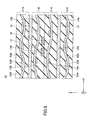
- FIG. 9 is a transparent plan view of main parts of a wiring substrate according to a second embodiment.
- FIG. 10 is a cross-sectional view of main parts of the wiring substrate according to the second embodiment. Some of the elements illustrated in FIG. 10 are not illustrated in FIG. 9 .
- FIG. 10 is a cross-sectional view cut along a line C-C in FIG. 9 .
- a reference 67, an insulating layer 61A, wirings 65 and 66, an insulating layer 61B, and a reference 68 are laminated in a wiring substrate 60. A detailed description is given of the respective components of the wiring substrate 60.
- the insulating layer 61A includes glass fiber bundles 62A, 63A, and 63B, and insulating resin 64A.
- the glass fiber bundles 62A, 63A, and 63B are impregnated by the insulating resin 64A.
- the materials of the insulating resin 64A are the same as those of the insulating resin 14A, and are thus not further described.
- the glass fiber bundles 62A having a width of W 3 are disposed in a direction parallel to an X axis with intervals of S 6 .
- the glass fiber bundles 63A having a width of W 4 are disposed in a direction parallel to a Y axis with intervals of S 7 .
- the glass fiber bundles 63B having a width of W 5 are disposed in a direction parallel to the Y axis with intervals of S 8 .
- the glass fiber bundles 62A, 63A, and 63B are plain-woven in a lattice-like manner.
- Each of the glass fiber bundles 62A, 63A, and 63B is formed by bundling together plural glass fibers of, for example, several millimeters.
- gap parts 62X spacedling together plural glass fibers of, for example, several millimeters.
- the gap parts 12X are filled with the insulating resin 64A.
- the width W 4 is wider than the width W 5
- the interval S 7 is wider than the interval S 8 .
- the insulating layer 61B includes glass fiber bundles 62B, 63C, and 63D, and insulating resin 64B.
- the glass fiber bundles 62B, 63C, and 63D are impregnated by the insulating resin 64B.
- the materials of the insulating resin 64B are the same as those of the insulating resin 14A, and are thus not further described.
- the glass fiber bundles 62B having a width of W 3 are disposed in a direction parallel to the X axis with intervals of S 6 .
- the glass fiber bundles 63C having a width of W 4 are disposed in a direction parallel to the Y axis with intervals of S 7 .
- the glass fiber bundles 63D having a width of W 5 are disposed in a direction parallel to the Y axis with intervals of S 8 .
- the glass fiber bundles 62B, 63C, and 63D are plain-woven in a lattice-like manner.
- the width W 3 may be equal to the width W 4
- the interval S 6 may be equal to the interval S 7 .
- the glass fiber bundles 62B, 63C, and 63D are disposed at positions corresponding to the glass fiber bundles 62A, 63A, and 63B. That is to say, the glass fiber bundles 62B, 63C, and 63D are disposed at positions overlapping the glass fiber bundles 62A, 63A, and 63B in a planar view.
- the wirings 65 and 66 are selectively formed on one side of the insulating layer 61A.
- the reference 67 is formed on substantially the entire surface of the other side of the insulating layer 61A.
- the reference 68 is formed on substantially the entire surface of the insulating layer 61B, on the side opposite to that adjacent to the wirings 65 and 66.
- the wirings 65 and 66 are conducting bodies through which predetermined electric signals flow.
- the references 67 and 68 are conducting bodies acting as return circuits of the predetermined electric signals flowing through the wirings 65 and 66.
- the wirings 65 and 66 correspond to differential signals.
- the materials of the wiring 65, etc., are the same as that of the wiring 15, etc., and are thus not further described.
- the width W 3 of the glass fiber bundle 62A (width W 3 of the glass fiber bundle 62B) and the width W 4 of the glass fiber bundle 63A (width W 4 of the glass fiber bundle 63B) may be any value, but are preferably narrower than the width of the wirings 65 and 66. More specifically, the width of conventional glass fiber bundles is approximately 300 ⁇ m. However, in the present embodiment, the width W 3 and the width W 4 are preferably narrower than the width of the wirings 65 and 66, at less than or equal to 100 ⁇ m, for example.
- the interval S 7 between the glass fiber bundles 63A (interval S 7 between the glass fiber bundles 63C) is set to be wider than "the width of the wiring 65 + the width of the wiring 66 + the interval between the wirings 65 and 66".
- the interval S 7 may be, for example, 800 ⁇ m.
- the width W 5 of the glass fiber bundle 63B (width W 5 of the glass fiber bundle 63D) is set to be narrower than the width of the wirings 65 and 66.
- the width W 5 may be, for example, less than or equal to 100 ⁇ m.
- the interval S 8 between the glass fiber bundles 63B (interval S 8 between the glass fiber bundle 63D) is set, for example, such that the interval S 7 between the glass fiber bundles 63A (interval S 7 between the glass fiber bundles 63C) is evenly divided.
- the number of glass fiber bundles 63B and 63D is not limited to three and may be any number.
- the interval S 7 between the glass fiber bundles 63A are set to be wider than "the width of the wiring 65 + the width of the wiring 66 + the interval between the wirings 65 and 66". Accordingly, the wirings 65 and 66 are disposed between adjacent glass fiber bundles 63A at positions that do not overlap the glass fiber bundles 63A in a planar view, and between adjacent glass fiber bundles 63C at positions that do not overlap the glass fiber bundles 63C in a planar view.
- the wirings 65 and 66 extend along the gap parts (so-called basket holes) filled with the insulating resin having a low relative permittivity and excellent transmission properties. Only few parts of the wirings 65 and 66 cross the glass fiber bundles. Therefore, compared to conventional wiring substrates, in the wiring substrate 60, the impact of differences in the glass fiber density is mitigated, and inconsistencies in characteristic impedance and differences in the propagation delay time are reduced, and high speed transmission is performed with high performance.
- the width W 3 of the glass fiber bundle 62A narrower than the widths of the wirings 65 and 66, even more parts of the wirings 65 and 66 extend along the insulating resin having a low relative permittivity and excellent transmission properties. Furthermore, even less parts of the wirings 65 and 66 cross the glass fiber bundles. Therefore, the impact of differences in the glass fiber density is mitigated even more, and inconsistencies in characteristic impedance and differences in the propagation delay time are reduced even more, and high speed transmission is performed with high performance.
- the glass fiber bundles 63B having a narrower width than the glass fiber bundles 63A are disposed between adjacent glass fiber bundles 63A
- the glass fiber bundles 63D having a narrower width than the glass fiber bundles 63C are disposed between adjacent glass fiber bundles 63C. Therefore, it is possible to compensate for the decrease in the amount of glass fiber, to prevent the strength of the wiring substrate 60 from decreasing, and to prevent the coefficient of thermal expansion from increasing.
- the width W 5 of the glass fiber bundles 63B and 63D are narrower than the widths of the wirings 65 and 66, and therefore high speed transmission is unaffected.
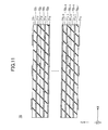
- a wiring substrate 70 includes multiple wiring layers 71 1 through 71 n that are laminated via insulating layers 72 1 through 72 n-1 in which glass fiber bundles (not illustrated) are woven in a lattice-like manner.
- the configuration illustrated in FIG. 4 is only applied to the wiring layer 71 3 and the insulating layers 72 1 through 72 4 .
- the widths and intervals of the glass fiber bundles in the other insulating layers do not affect the high speed transmission in the differential wirings in the wiring layer 71 3 . Therefore, the widths and intervals of the glass fiber bundles in the other insulating layers may be appropriately set in consideration of preventing the strength of the wiring substrate 70 from decreasing, and preventing the coefficient of thermal expansion from increasing.
- the configuration illustrated in FIG. 10 is only applied to the wiring layer 71 3 and the insulating layers insulating layers 72 2 and 72 3 .
- the widths and intervals of the glass fiber bundles in the other insulating layers do not affect the high speed transmission in the differential wirings in the wiring layer 71 3 . Therefore, the widths and intervals of the glass fiber bundles in the other insulating layers may be appropriately set in consideration of preventing the strength of the wiring substrate 70 from decreasing, and preventing the coefficient of thermal expansion from increasing.
- a core layer 82 is prepared by forming solid copper foil 17 and 81 as wiring layers on both sides of the insulating layer 11A. Then, reference holes 82X are formed in the core layer 82. For example, two reference holes 82X are formed in opposing corners.
- FIG. 12 is a transparent plan view
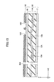
- FIG. 13 is a cross-sectional view cut along a line C-C in FIG. 12 . Some of the elements illustrated in FIG. 13 are not illustrated in FIG. 12 .
- the solid copper foil 17 corresponds to the reference 17 described above.
- an X ray is radiated onto the core layer 82 to recognize the positions of the glass fiber bundles 12A and 13A, and an origin position R is determined.
- the origin position R may be any position; however, in this case, one of the apexes of the gap parts 12X formed by the glass fiber bundles 12A and 13A is determined as the origin position R.
- the reference holes 82X that pass through the core layer 82 are formed at predetermined positions by using the determined origin position R as a reference. Information relevant to the widths and intervals of the glass fiber bundles 12A and 13A is recognized in advance as design information. Therefore, it is possible to calculate coordinates of an area where the glass fiber bundles 12A and 13A are located, with respect to the reference hole 82X.
- the wirings 15 and 16 which are differential wirings are formed.
- a resist layer 83 is formed on the solid copper foil 81 which is the wiring layer.
- a mask 84 is positioned on the resist layer 83.
- the mask 84 includes positioning holes 84X (reference marks) corresponding to the reference holes 82X of the core layer 82, and openings 15X and 16X corresponding to the wirings 15 and 16.
- the positioning holes 84X and the openings 15X and 16X are formed in advance.
- the mask 84 is fabricated such that the openings 15X and 16X are positioned between adjacent glass fiber bundles 12A or between adjacent glass fiber bundles 13A, when the positioning holes 84X are positioned to match the positions of the reference holes 82X.
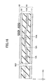
- the resist layer 83 is exposed and developed via the mask 84. Accordingly, as illustrated in FIG. 16 , the resist layer 83 is partially removed so that the resist layer 83 only remains at positions corresponding to where the wirings 15 and 16 are formed on the solid copper foil 81. Then, as illustrated in FIG. 17 , the resist layer 83 is used as a mask to perform etching on the solid copper foil 81. Subsequently, the resist layer 83 is removed, so that the wirings 15 and 16 are formed.
- the insulating layer 11B is prepared, and reference holes 11X are formed (at two positions) at the same positions as the reference holes 82X of the core layer 82 illustrated in FIGS. 12 and 13 . That is to say, the positions of the reference holes 11X are formed such that when the reference holes 11X are positioned to match the positions of the reference holes 82X, the center positions of the glass fiber bundles 12A and the center positions of the glass fiber bundles 12B match each other and the center positions of the glass fiber bundles 13A and the center positions of the glass fiber bundles 13B match each other. Then, by performing pin lamination, the positions of the core layer 82 and insulating layer 11B are matched. Specifically, as illustrated in FIG.
- a mounting part 89 provided with positioning pins 88 is used to position the core layer 82 and the insulating layer 11B, and the insulating layer 11B is fixed on the core layer 82.
- the mounting part 89 is provided with two positioning pins 88 provided at positions corresponding to the two reference holes 82X of the insulating layer 11A illustrated in FIGS. 12 and 13 , and at positions corresponding to the two reference holes 11X of the insulating layer 11B.
- the core layer 82 and the insulating layer 11B are removed from the mounting part 89 provided with the positioning pin 88, so that a laminated body including the insulating layer 11B fixed on the core layer 82 is formed as illustrated in FIG. 19 .
- an X ray is radiated onto the insulating layer to recognize the positions of the glass fiber bundles and determine the origin position R.
- the determined origin position R As a reference, reference holes are formed at predetermined positions to pass through the insulating film. It is possible to recognize the positions of the glass fiber bundles with respect to the reference holes, and therefore differential wirings are formed between adjacent glass fiber bundles. Then, the same method is performed to form reference holes in another insulating layer. Then, the other insulating layer is positioned on the insulating layer with differential wirings by pin lamination, and the other insulating layer is laminated onto the insulating layer with differential wirings.
- the differential wirings are disposed between two adjacent glass fiber bundles at positions that do not overlap the glass fiber bundles in a planar view. Furthermore, the differential wirings are disposed between two adjacent glass fiber bundles of the other insulating layer at positions that do not overlap the glass fiber bundles of the other insulating layer in a planar view.
- the insulating layer 21A is laminated on the laminated body in which the insulating layer 11B is fixed on the core layer 82, the positional relationships between the glass fiber bundles 12A and 13A and the glass fiber bundles 22A and 23A are not that important.
- the glass fiber bundles 22A and 23A are for reinforcing the gap parts 12X. As long as the glass fiber bundles 22A and 23A are located above the gap parts 12X, their purposes are fulfilled. The same applies when laminating the insulating layer 21B.
- the manufacturing method of the wiring substrate 10 is also applicable to the wiring substrate 30 according to modification 1 of the first embodiment, the wiring substrate 40 according to modification 2 of the first embodiment, the wiring substrate 50 according to modification 3 of the first embodiment, and the wiring substrate 60 according to the second embodiment.
- glass fiber bundles that are narrower than the glass fiber bundles 62A and 62B may be provided in a direction parallel to the X axis, between adjacent glass fiber bundles 62A or adjacent glass fiber bundles 62B.
- a wiring substrate is provided with low manufacturing costs, in which the impact of differences in the glass fiber density on the wirings is minimized.
Landscapes
- Engineering & Computer Science (AREA)
- Microelectronics & Electronic Packaging (AREA)
- Production Of Multi-Layered Print Wiring Board (AREA)
- Structure Of Printed Boards (AREA)
Abstract
Description
- The embodiments discussed herein are related to a wiring substrate in which differential wirings are formed on an insulating layer.
- An object of a conventional technology is to avoid accumulation of phase shift on one of a P wiring and an N wiring, by arranging yarn of a glass cloth parallel to an extending direction of wirings so that the yarn intersects the differential wirings in a zig-zag manner, and to therefore prevent generation of skew between the wirings.
-
Warp yarn 4 and weft yarn 5 constituting glass cloth used for forming a substrate for lamination are arranged so that one or both of thewarp yarn 4 and the weft yarn 5 are arranged in a zig-zag manner by a length equal to the total of the widths of differential wirings and the distances between the wirings. Accordingly, the variation in the relative dielectric constant of the substrate for lamination is averaged, thus mitigating the deterioration of waveform quality in differential transmission. - Patent document 1 : Japanese Laid-Open Patent Publication No.
2009-73946 - Accordingly, it is an object in one aspect of the invention to provide a wiring substrate with low manufacturing costs, in which the impact of differences in the glass fiber density on the wirings is minimized.
- According to an aspect of the invention, a wiring substrate includes a pair of differential wirings; a first insulating layer that is provided adjacent to one side of the pair of differential wirings, the first insulating layer including first fiber bundles disposed in parallel to an extending direction of the pair of differential wirings; a second insulating layer that is provided adjacent to another side of the pair of differential wirings, the second insulating layer including second fiber bundles disposed in parallel to the extending direction of the pair of differential wirings, the second fiber bundles being disposed by the same pitch as the first fiber bundles; a third insulating layer that is provided on a side of the first insulating layer opposite to a side of the first insulating layer that is adjacent to the pair of differential wirings, the third insulating layer including third fiber bundles disposed in parallel to the extending direction of the pair of differential wirings; and a fourth insulating layer that is provided on a side of the second insulating layer opposite to a side of the second insulating layer that is adjacent to the pair of differential wirings, the fourth insulating layer including fourth fiber bundles disposed in parallel to the extending direction of the pair of differential wirings, wherein intervals between the third fiber bundles and intervals between the fourth fiber bundles are respectively narrower than intervals between the first fiber bundles and intervals between the second fiber bundles, and the pair of differential wirings are disposed between adjacent ones of the first fiber bundles at positions that do not overlap the first fiber bundles in a planar view, and are disposed between adjacent ones of the second fiber bundles at positions that do not overlap the second fiber bundles in a planar view.
-
-
FIG. 1 is a transparent plan view of main parts of a conventional wiring substrate; -
FIG. 2 is a cross-sectional view of main parts of the conventional wiring substrate; -
FIG. 3 is a transparent plan view of main parts of a wiring substrate according to a first embodiment; -
FIG. 4 is a cross-sectional view of main parts of the wiring substrate according to the first embodiment; -
FIG. 5 illustrates examples of glass fiber bundles in an insulating layer; -
FIG. 6 is a transparent plan view of main parts of a wiring substrate according tomodification 1 of the first embodiment; -
FIG. 7 is a cross-sectional view of main parts of a wiring substrate according tomodification 2 of the first embodiment; -
FIG. 8 is a cross-sectional view of main parts of a wiring substrate according tomodification 3 of the first embodiment; -
FIG. 9 is a transparent plan view of main parts of a wiring substrate according to a second embodiment; -
FIG. 10 is a cross-sectional view of main parts of the wiring substrate according to the second embodiment; -
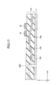
FIG. 11 is for describing a wiring substrate including multiple layers; -
FIG. 12 is for describing a manufacturing method of the wiring substrate illustrated inFIGS. 3 and4 (part 1); -
FIG. 13 is for describing the manufacturing method of the wiring substrate illustrated inFIGS. 3 and4 (part 2); -
FIG. 14 is for describing the manufacturing method of the wiring substrate illustrated inFIGS. 3 and4 (part 3); -
FIG. 15 is for describing the manufacturing method of the wiring substrate illustrated inFIGS. 3 and4 (part 4); -
FIG. 16 is for describing the manufacturing method of the wiring substrate illustrated inFIGS. 3 and4 (part 5); -
FIG. 17 is for describing the manufacturing method of the wiring substrate illustrated inFIGS. 3 and4 (part 6); -
FIG. 18 is for describing the manufacturing method of the wiring substrate illustrated inFIGS. 3 and4 (part 7); and -
FIG. 19 is for describing the manufacturing method of the wiring substrate illustrated inFIGS. 3 and4 (part 8). - Preferred embodiments of the present invention will be explained with reference to accompanying drawings. Throughout the drawings, common components are denoted by the same reference numerals, and redundant descriptions may be omitted.
-
FIG. 1 is a transparent plan view of main parts of an example of a wiring substrate.FIG. 2 is a cross-sectional view of main parts of the example of the wiring substrate. Some of the elements illustrated inFIG. 2 are not illustrated inFIG. 1 .FIG. 2 is a cross-sectional view cut along a line A-A inFIG. 1 . - As illustrated in
FIG. 1 andFIG. 2 , in an example of awiring substrate 100, areference 170, aninsulating layer 110A,wirings insulating layer 110B, and areference 180 are laminated. - The
insulating layer 110A includesglass fiber bundles resin 140A. Theglass fiber bundles insulating resin 140A. Theinsulating layer 110B includesglass fiber bundles resin 140B. Theglass fiber bundles insulating resin 140B. - The
glass fiber bundles 120A are disposed in a direction parallel to an X axis, and theglass fiber bundles 130A are disposed in a direction parallel to a Y axis. Theglass fiber bundles glass fiber bundles 120B are disposed in a direction parallel to an X axis, and theglass fiber bundles 130B are disposed in a direction parallel to a Y axis. Theglass fiber bundles glass fiber bundles glass fiber bundles - The
wirings insulating layer 110A. Thereference 170 is formed on substantially the entire surface of the other side of theinsulating layer 110A. Thereference 180 is formed on substantially the entire surface of theinsulating layer 110B, on the side opposite to that adjacent to thewirings wirings references wirings - The
wirings wiring 150 is disposed on one of theglass fiber bundles 130A, while thewiring 160 is disposed between theglass fiber bundle 130A on which thewiring 150 is disposed and an adjacentglass fiber bundle 130A (between adjacentglass fiber bundles 130A). - In recent years, wirings have become thinner than the pitches between glass fiber bundles. Therefore, in many cases, a wiring substrate includes wirings positioned on glass fiber bundles as well as wirings positioned between glass fiber bundles. The relative permittivity on a glass fiber bundle is different from the relative permittivity between glass fiber bundles (on the insulating resin), due to the difference in the glass fiber density. Therefore, when there are wirings positioned on glass fiber bundles as well as wirings positioned between glass fiber bundles, there may be inconsistencies in characteristic impedance and differences in the propagation delay time. Particularly, in recent years, the frequency of high-speed transmission has approached a range of 3 GHz through 5 GHz, and therefore problems are arising in connection with inconsistencies in characteristic impedance and differences in the propagation delay time.
- In order to solve such problems, there is a technology of arranging the wirings in a zig-zag manner by changing the angle of the wirings at a certain length with respect to the glass fiber bundles that are plain-woven in a lattice-like manner. There is also a technology of propagating high frequency signals by using a low-dielectric material as the material of the wiring substrate. Furthermore, in order to achieve the same effects as the technology of arranging the wirings in a zig-zag manner, there is a technology of tilting the wiring substrate and laminating layers.
- However, the technology of arranging wirings in a zig-zag manner uses excessive wirings, and therefore the manufacturing cost is increased. Furthermore, with the technology of propagating high frequency signals by using a low-dielectric material as the material of the wiring substrate, the low-dielectric material is expensive, and therefore the manufacturing cost is increased. Furthermore, with the technology of tilting the wiring substrate and laminating layers, the material efficiency significantly decreases as the tilt angle increases, and therefore the manufacturing cost is increased.
-
FIG. 3 is a transparent plan view of main parts of a wiring substrate according to a first embodiment.FIG. 4 is a cross-sectional view of main parts of the wiring substrate according to the first embodiment. Some of the elements illustrated inFIG. 4 are not illustrated inFIG. 3 .FIG. 4 is a cross-sectional view cut along a line B-B inFIG. 3 . As illustrated inFIGS. 3 and4 , in awiring substrate 10, an insulatinglayer 21A, areference 17, an insulatinglayer 11A, wirings 15 and 16, an insulatinglayer 11B, areference 18, and an insulatinglayer 21B are laminated. A detailed description is given of the respective components of thewiring substrate 10. - The insulating
layer 11A includesglass fiber bundles resin 14A. Theglass fiber bundles resin 14A. The insulatingresin 14A may be made of a material such as epoxy resin, polymide resin, and polyester resin. The insulatingresin 14A may include filler such as silica and alumina. - The
glass fiber bundles 12A having a width of W1 are disposed in a direction parallel to an X axis with intervals of S1. Theglass fiber bundles 13A having a width of W2 are disposed in a direction parallel to a Y axis with intervals of S2. Theglass fiber bundles glass fiber bundles
Atgap parts 12X (so-called basket holes) formed by theglass fiber bundles gap parts 12X are filled with the insulatingresin 14A. - The insulating
layer 11B includesglass fiber bundles resin 14B. Theglass fiber bundles resin 14B. The insulatingresin 14B may be made of the same material as that of the insulatingresin 14A, and is thus not further described. - The
glass fiber bundles 12B having a width of W1 are disposed in a direction parallel to the X axis with intervals of S1. Theglass fiber bundles 13B having a width of W2 are disposed in a direction parallel to the Y axis with intervals of S2. Theglass fiber bundles glass fiber bundles glass fiber bundles - The
glass fiber bundles glass fiber bundles glass fiber bundles glass fiber bundles FIGS. 3 and4 . - As long as the
glass fiber bundles glass fiber bundles - Instead of bundling together plural glass fibers to form the
glass fiber bundles 12A, fiber bundles may be formed by bundling together carbon fibers, polyester fibers, Tetron fibers, nylon fibers, aramid fibers, or the like. The method of weaving theglass fiber bundles 12A (or other fiber bundles) is not limited to plain-weaving; the fiber bundles may be woven by sateen weaving, twill weaving, or the like. - The
wirings layer 11A. Thereference 17 is formed on substantially the entire surface of the other side of the insulatinglayer 11A. Thereference 18 is formed on substantially the entire surface of the insulatinglayer 11B, on the side opposite to that adjacent to thewirings wirings references wirings wiring 15 and thereference 17, etc., are not particularly limited as long as they are conducting bodies. For example, Cu, Al, Au, and Ag may be used. - The
wirings wiring 15, and NEG signals flow through thewiring 16 that is disposed in parallel with thewiring 15. High speed transmission is performed with is high performance, as long as there are no inconsistencies in characteristic impedance and no differences in the propagation delay time between thewiring 15 and thewiring 16. - The
wirings glass fiber bundles 12A at positions that do not overlap theglass fiber bundles 12A in a planar view, and between adjacentglass fiber bundles 13A at positions that do not overlap theglass fiber bundles 13A in a planar view. Furthermore, thewirings glass fiber bundles 12B at positions that do not overlap theglass fiber bundles 12B in a planar view, and between adjacentglass fiber bundles 13B at positions that do not overlap the glass fiber bundles 13B in a planar view. The width of thewirings wirings - The width W1 of the
glass fiber bundle 12A (width W1 of theglass fiber bundle 12B) and the width W2 of theglass fiber bundle 13A (width W2 of theglass fiber bundle 13B) may be any value, but are preferably narrower than the width of thewirings wirings - The interval S1 between the
glass fiber bundles 12A (interval S1 between theglass fiber bundles 12B) and the interval S2 between theglass fiber bundles 13A (interval S2 between theglass fiber bundle 13B) are set to be wider than "the width of thewiring 15 + the width of thewiring 16 + the interval between thewirings - As described above, the intervals S1 and S2 between the glass fiber bundles are set to be wider than "the width of the
wiring 15 + the width of thewiring 16 + the interval between thewirings wirings glass fiber bundles 12A at positions that do not overlap theglass fiber bundles 12A in a planar view, and between adjacentglass fiber bundles 13A at positions that do not overlap theglass fiber bundles 13A in a planar view. Furthermore, thewirings glass fiber bundles 12B at positions that do not overlap theglass fiber bundles 12B in a planar view, and between adjacentglass fiber bundles 13B at positions that do not overlap the glass fiber bundles 13B in a planar view. Consequently, most parts of thewirings wirings - Furthermore, the manufacturing cost is prevented from increasing, compared to conventional methods in which an expensive low-dielectric material is used to form the wiring substrate, or the wiring substrate is tilted to laminate layers.
- Particularly, by making the widths W1 and W2 of the glass fiber bundles narrower than the width of the
wirings wirings wirings - The intervals S1 and S2 between the glass fiber bundles are set to be wider than "the width of the
wiring 15 + the width of thewiring 16 + the interval between thewirings - In the
wiring substrate 10, the widths of the glass fiber bundles are narrower and the intervals are wider than those of conventional wiring substrates. Therefore, compared to conventional wiring substrates, thewiring substrate 10 includes a smaller amount of glass fiber per unit area and a larger amount of insulating resin per unit area. Accordingly, the strength of thewiring substrate 10 may be insufficient, and the coefficient of thermal expansion may increase. In order to avoid such problems, in the present embodiment, the insulatinglayers wiring substrate 10. The roles of the insulatinglayers -
FIG. 5 illustrates examples of glass fiber bundles in the insulatinglayer 21A. Referring toFIGS. 4 and5 , the insulatinglayer 21A includesglass fiber bundles resin 24A. Theglass fiber bundles resin 24A. The materials of the insulatingresin 24A are the same as those of the insulatingresin 14A, and are thus not further described. - The
glass fiber bundles 22A have the same width W1 as theglass fiber bundles 12A, and are disposed in a direction parallel to the X axis with narrower intervals S3 than those of theglass fiber bundles 12A. Theglass fiber bundles 23A have the same width W2 as theglass fiber bundles 13A, and are disposed in a direction parallel to the Y axis with narrower intervals S4 than those of theglass fiber bundles 13A. Theglass fiber bundles 22A and theglass fiber bundles 23A are plain-woven in a lattice-like manner. Details of theglass fiber bundles glass fiber bundles - The insulating
layer 21B includesglass fiber bundles resin 24B. Theglass fiber bundles resin 24B. The materials of the insulatingresin 24B are the same as those of the insulatingresin 14A, etc., and are thus not further described. - The
glass fiber bundles 22B have the same width W1 as theglass fiber bundles 12B, and are disposed in a direction parallel to the X axis with narrower intervals S3 than those of theglass fiber bundles 12B. Theglass fiber bundles 23B have the same width W2 as theglass fiber bundles 13B, and are disposed in a direction parallel to the Y axis with narrower intervals S4 than those of the glass fiber bundles 13B. Theglass fiber bundles 22B and theglass fiber bundles 23B are plain-woven in a lattice-like manner. Details of theglass fiber bundles glass fiber bundles - As described above, the insulating
layer 21A includes theglass fiber bundles 22A that have the same width W1 as theglass fiber bundles 12A and that are disposed with narrower intervals S3 than the intervals S1 between theglass fiber bundles 12A, and theglass fiber bundles 23A that have the same width W2 as theglass fiber bundles 13A and that are disposed with narrower intervals S4 than the intervals S2 between theglass fiber bundles 13A. Furthermore, the insulatinglayer 21B includes theglass fiber bundles 22B that have the same width W1 as theglass fiber bundles 12B and that are disposed with narrower intervals S3 than the intervals S1 between theglass fiber bundles 12B, and theglass fiber bundles 23B that have the same width W2 as theglass fiber bundles 13B and that are disposed with narrower intervals S4 than the intervals S2 between the glass fiber bundles 13B. Theglass fiber bundles layers wiring substrate 10 from decreasing, and to prevent the coefficient of thermal expansion from increasing. - As described above, in the present embodiment, the width W1 of the
glass fiber bundles glass fiber bundles glass fiber bundles glass fiber bundles wirings glass fiber bundles 12A at positions that do not overlap theglass fiber bundles 12A in a planar view, and between adjacentglass fiber bundles 13A at positions that do not overlap theglass fiber bundles 13A in a planar view. Furthermore, thewirings glass fiber bundles 12B at positions that do not overlap theglass fiber bundles 12B in a planar view, and between adjacentglass fiber bundles 13B at positions that do not overlap the glass fiber bundles 13B in a planar view. Consequently, most parts of thewirings wirings wiring substrate 10, the impact of differences in the glass fiber density is mitigated, and inconsistencies in characteristic impedance and differences in the propagation delay time are reduced, and high speed transmission is performed with high performance. - Furthermore, in the present embodiment, the insulating
layers layers layers layers layers wiring substrate 10 from decreasing, and to prevent the coefficient of thermal expansion from increasing. - Furthermore, the difference in the propagation delay time (difference between the propagation delay time of the
wiring 15 and the propagation delay time of the wiring 16) in thewiring substrate 10 according to the present embodiment was measured, and the measurement result was 5 ps/100 mm. Meanwhile, the difference in the propagation delay time in theconventional wiring substrate 100 was measured, and the measurement result was 7 ps/100 mm. Accordingly, it was found that in thewiring substrate 10 according to the present embodiment, the difference in the propagation delay time is reduced by approximately 30% compared to that of theconventional wiring substrate 100. -
FIG. 6 is a transparent plan view of main parts of a wiring substrate according tomodification 1 of the first embodiment. Awiring substrate 30 illustrated inFIG. 6 is different from thewiring substrate 10 illustrated inFIGS. 3 and4 in that theglass fiber bundles 12A is replaced withglass fiber bundles 32A andglass fiber bundles 12B are replaced with glass fiber bundles 32B (not illustrated), and thewirings wirings wiring substrate 30 that are different from those of thewiring substrate 10, and other features are not further described. - The width W1 of the
glass fiber bundles 32A and 32B are the same as those of theglass fiber bundles glass fiber bundles 32A and 32B are narrower than the intervals S1 between theglass fiber bundles glass fiber bundles 32A. That is to say, the glass fiber bundles 32B are provided at positions overlapping theglass fiber bundles 32A in a planar view. Thewirings glass fiber bundles 13A at positions that do not overlap theglass fiber bundles 13A in a planar view, and between adjacentglass fiber bundles 13B at positions that do not overlap the glass fiber bundles 13B in a planar view. - As described above, when the
wirings wiring substrate 30 may have the following configuration. That is, the intervals between glass fiber bundles in only one direction are to be set to be wider than "the width of thewiring 35 + the width of thewiring 36 + the interval between thewirings wirings glass fiber bundles 13A at positions that do not overlap theglass fiber bundles 13A in a planar view, and between adjacentglass fiber bundles 13B at positions that do not overlap the glass fiber bundles 13B in a planar view. Consequently, most parts of thewirings wirings - However, more parts of the
wirings wiring substrate 10 illustrated inFIG. 3 . Therefore, the first embodiment is more preferable for further mitigating the inconsistencies in characteristic impedance and the impact of differences in the glass fiber density. -
FIG. 7 is a cross-sectional view of main parts of the wiring substrate according tomodification 2 of the first embodiment. Awiring substrate 40 illustrated inFIG. 7 is different from thewiring substrate 10 illustrated inFIGS. 3 and4 in that theglass fiber bundles glass fiber bundles wiring substrate 40 that are different from those of thewiring substrate 10, and other features are not further described. - The widths of the
glass fiber bundles glass fiber bundles glass fiber bundles glass fiber bundles - By making the
glass fiber bundles glass fiber bundles wirings glass fiber bundles glass fiber bundles layers glass fiber bundles glass fiber bundles - Even when the
glass fiber bundles layers wiring substrate 40 from decreasing, and to prevent the coefficient of thermal expansion from increasing. -
FIG. 8 is a cross-sectional view of main parts of the wiring substrate according tomodification 3 of the first embodiment. Awiring substrate 50 illustrated inFIG. 8 is different from thewiring substrate 10 illustrated inFIGS. 3 and4 in that theglass fiber bundles glass fiber bundles wiring substrate 50 that are different from those of thewiring substrate 10, and other features are not further described. - The widths of the
glass fiber bundles glass fiber bundles glass fiber bundles glass fiber bundles - When the insulating
layers glass fiber bundles FIG. 8 , the widths of theglass fiber bundles glass fiber bundles wiring substrate 10 may be efficiently prevented from decreasing, and the coefficient of thermal expansion may be efficiently prevented from increasing. -
FIG. 9 is a transparent plan view of main parts of a wiring substrate according to a second embodiment.FIG. 10 is a cross-sectional view of main parts of the wiring substrate according to the second embodiment. Some of the elements illustrated inFIG. 10 are not illustrated inFIG. 9 .FIG. 10 is a cross-sectional view cut along a line C-C inFIG. 9 . As illustrated inFIGS. 9 and10 , areference 67, an insulatinglayer 61A, wirings 65 and 66, an insulatinglayer 61B, and areference 68 are laminated in awiring substrate 60. A detailed description is given of the respective components of thewiring substrate 60. - The insulating
layer 61A includesglass fiber bundles resin 64A. Theglass fiber bundles resin 64A. The materials of the insulatingresin 64A are the same as those of the insulatingresin 14A, and are thus not further described. - The
glass fiber bundles 62A having a width of W3 are disposed in a direction parallel to an X axis with intervals of S6. Theglass fiber bundles 63A having a width of W4 are disposed in a direction parallel to a Y axis with intervals of S7. In between adjacentglass fiber bundles 63A, theglass fiber bundles 63B having a width of W5 are disposed in a direction parallel to the Y axis with intervals of S8. Theglass fiber bundles glass fiber bundles gap parts 62X (so-called basket holes) formed by theglass fiber bundles 62A and theglass fiber bundles gap parts 12X are filled with the insulatingresin 64A. The width W4 is wider than the width W5, and the interval S7 is wider than the interval S8. - The insulating
layer 61B includesglass fiber bundles resin 64B. Theglass fiber bundles resin 64B. The materials of the insulatingresin 64B are the same as those of the insulatingresin 14A, and are thus not further described. - The
glass fiber bundles 62B having a width of W3 are disposed in a direction parallel to the X axis with intervals of S6. Theglass fiber bundles 63C having a width of W4 are disposed in a direction parallel to the Y axis with intervals of S7. In between adjacentglass fiber bundles 63C, theglass fiber bundles 63D having a width of W5 are disposed in a direction parallel to the Y axis with intervals of S8. Theglass fiber bundles glass fiber bundles glass fiber bundles - The
glass fiber bundles glass fiber bundles glass fiber bundles glass fiber bundles - The
wirings layer 61A. Thereference 67 is formed on substantially the entire surface of the other side of the insulatinglayer 61A. Thereference 68 is formed on substantially the entire surface of the insulatinglayer 61B, on the side opposite to that adjacent to thewirings wirings references wirings wirings wiring 65, etc., are the same as that of thewiring 15, etc., and are thus not further described. - The width W3 of the
glass fiber bundle 62A (width W3 of theglass fiber bundle 62B) and the width W4 of theglass fiber bundle 63A (width W4 of theglass fiber bundle 63B) may be any value, but are preferably narrower than the width of thewirings wirings - The interval S7 between the
glass fiber bundles 63A (interval S7 between theglass fiber bundles 63C) is set to be wider than "the width of thewiring 65 + the width of thewiring 66 + the interval between thewirings - The width W5 of the
glass fiber bundle 63B (width W5 of theglass fiber bundle 63D) is set to be narrower than the width of thewirings glass fiber bundles 63B (interval S8 between theglass fiber bundle 63D) is set, for example, such that the interval S7 between theglass fiber bundles 63A (interval S7 between theglass fiber bundles 63C) is evenly divided. The number ofglass fiber bundles - As described above, the interval S7 between the
glass fiber bundles 63A are set to be wider than "the width of thewiring 65 + the width of thewiring 66 + the interval between thewirings wirings glass fiber bundles 63A at positions that do not overlap theglass fiber bundles 63A in a planar view, and between adjacentglass fiber bundles 63C at positions that do not overlap theglass fiber bundles 63C in a planar view. - Consequently, most parts of the
wirings wirings wiring substrate 60, the impact of differences in the glass fiber density is mitigated, and inconsistencies in characteristic impedance and differences in the propagation delay time are reduced, and high speed transmission is performed with high performance. - Particularly, by making the width W3 of the
glass fiber bundle 62A narrower than the widths of thewirings wirings wirings - Furthermore, the
glass fiber bundles 63B having a narrower width than theglass fiber bundles 63A are disposed between adjacentglass fiber bundles 63A, and theglass fiber bundles 63D having a narrower width than theglass fiber bundles 63C are disposed between adjacentglass fiber bundles 63C. Therefore, it is possible to compensate for the decrease in the amount of glass fiber, to prevent the strength of thewiring substrate 60 from decreasing, and to prevent the coefficient of thermal expansion from increasing. The width W5 of theglass fiber bundles wirings - As illustrated in
FIG. 11 , awiring substrate 70 includes multiple wiring layers 711 through 71n that are laminated via insulating layers 721 through 72n-1 in which glass fiber bundles (not illustrated) are woven in a lattice-like manner. In this case, not all of the wiring layers and insulating layers need to have the configuration of the first or second embodiments. For example, if the wiring layer 713 is the wiring layer with differential wirings, the configuration illustrated inFIG. 4 is only applied to the wiring layer 713 and the insulating layers 721 through 724. The widths and intervals of the glass fiber bundles in the other insulating layers do not affect the high speed transmission in the differential wirings in the wiring layer 713. Therefore, the widths and intervals of the glass fiber bundles in the other insulating layers may be appropriately set in consideration of preventing the strength of thewiring substrate 70 from decreasing, and preventing the coefficient of thermal expansion from increasing. - When the wiring layer 713 is the wiring layer with the differential wirings, the configuration illustrated in
FIG. 10 is only applied to the wiring layer 713 and the insulating layers insulating layers 722 and 723. The widths and intervals of the glass fiber bundles in the other insulating layers do not affect the high speed transmission in the differential wirings in the wiring layer 713. Therefore, the widths and intervals of the glass fiber bundles in the other insulating layers may be appropriately set in consideration of preventing the strength of thewiring substrate 70 from decreasing, and preventing the coefficient of thermal expansion from increasing. - Next, a description is given of a manufacturing method of the
wiring substrate 10 illustrated inFIGS. 3 and4 , with reference toFIGS. 12 through 19 . In the following, a description is given only of laminating/forming thereference 17, the insulatinglayer 11A, thewirings layer 11B. The other elements may be manufactured by the same method. - First, as illustrated in
FIGS. 12 and13 , acore layer 82 is prepared by formingsolid copper foil layer 11A. Then,reference holes 82X are formed in thecore layer 82. For example, tworeference holes 82X are formed in opposing corners.FIG. 12 is a transparent plan view, andFIG. 13 is a cross-sectional view cut along a line C-C inFIG. 12 . Some of the elements illustrated inFIG. 13 are not illustrated inFIG. 12 . Thesolid copper foil 17 corresponds to thereference 17 described above. - Specifically, for example, an X ray is radiated onto the
core layer 82 to recognize the positions of theglass fiber bundles gap parts 12X formed by theglass fiber bundles reference holes 82X that pass through thecore layer 82 are formed at predetermined positions by using the determined origin position R as a reference. Information relevant to the widths and intervals of theglass fiber bundles glass fiber bundles reference hole 82X. - Next, the
wirings FIG. 14 , a resistlayer 83 is formed on thesolid copper foil 81 which is the wiring layer. Then, as illustrated inFIG. 15 , amask 84 is positioned on the resistlayer 83. Themask 84 includespositioning holes 84X (reference marks) corresponding to the reference holes 82X of thecore layer 82, andopenings wirings openings glass fiber bundles reference hole 82X are calculated in advance. Therefore, themask 84 is fabricated such that theopenings glass fiber bundles 12A or between adjacentglass fiber bundles 13A, when the positioning holes 84X are positioned to match the positions of the reference holes 82X. - Next, the resist
layer 83 is exposed and developed via themask 84. Accordingly, as illustrated inFIG. 16 , the resistlayer 83 is partially removed so that the resistlayer 83 only remains at positions corresponding to where thewirings solid copper foil 81. Then, as illustrated inFIG. 17 , the resistlayer 83 is used as a mask to perform etching on thesolid copper foil 81. Subsequently, the resistlayer 83 is removed, so that thewirings - Next, the insulating
layer 11B is prepared, andreference holes 11X are formed (at two positions) at the same positions as the reference holes 82X of thecore layer 82 illustrated inFIGS. 12 and13 . That is to say, the positions of thereference holes 11X are formed such that when thereference holes 11X are positioned to match the positions of thereference holes 82X, the center positions of theglass fiber bundles 12A and the center positions of theglass fiber bundles 12B match each other and the center positions of theglass fiber bundles 13A and the center positions of theglass fiber bundles 13B match each other. Then, by performing pin lamination, the positions of thecore layer 82 and insulatinglayer 11B are matched. Specifically, as illustrated inFIG. 18 , a mountingpart 89 provided with positioning pins 88 is used to position thecore layer 82 and the insulatinglayer 11B, and the insulatinglayer 11B is fixed on thecore layer 82. The mountingpart 89 is provided with two positioningpins 88 provided at positions corresponding to the tworeference holes 82X of the insulatinglayer 11A illustrated inFIGS. 12 and13 , and at positions corresponding to the tworeference holes 11X of the insulatinglayer 11B. Subsequently, thecore layer 82 and the insulatinglayer 11B are removed from the mountingpart 89 provided with thepositioning pin 88, so that a laminated body including the insulatinglayer 11B fixed on thecore layer 82 is formed as illustrated inFIG. 19 . - As described above, an X ray is radiated onto the insulating layer to recognize the positions of the glass fiber bundles and determine the origin position R. By using the determined origin position R as a reference, reference holes are formed at predetermined positions to pass through the insulating film. It is possible to recognize the positions of the glass fiber bundles with respect to the reference holes, and therefore differential wirings are formed between adjacent glass fiber bundles. Then, the same method is performed to form reference holes in another insulating layer. Then, the other insulating layer is positioned on the insulating layer with differential wirings by pin lamination, and the other insulating layer is laminated onto the insulating layer with differential wirings. Consequently, on the insulating layer with the differential wirings, the differential wirings are disposed between two adjacent glass fiber bundles at positions that do not overlap the glass fiber bundles in a planar view. Furthermore, the differential wirings are disposed between two adjacent glass fiber bundles of the other insulating layer at positions that do not overlap the glass fiber bundles of the other insulating layer in a planar view.
- Furthermore, when the insulating
layer 21A is laminated on the laminated body in which the insulatinglayer 11B is fixed on thecore layer 82, the positional relationships between theglass fiber bundles glass fiber bundles glass fiber bundles gap parts 12X. As long as theglass fiber bundles gap parts 12X, their purposes are fulfilled. The same applies when laminating the insulatinglayer 21B. - The manufacturing method of the
wiring substrate 10 is also applicable to thewiring substrate 30 according tomodification 1 of the first embodiment, thewiring substrate 40 according tomodification 2 of the first embodiment, thewiring substrate 50 according tomodification 3 of the first embodiment, and thewiring substrate 60 according to the second embodiment. - The present invention is not limited to the specific embodiments described herein, and variations and modifications may be made without departing from the scope of the present invention.
- For example, in the second embodiment, glass fiber bundles that are narrower than the
glass fiber bundles glass fiber bundles 62A or adjacentglass fiber bundles 62B. - According to one embodiment of the present invention, a wiring substrate is provided with low manufacturing costs, in which the impact of differences in the glass fiber density on the wirings is minimized.
- All examples and conditional language recited herein are intended for pedagogical purposes to aid the reader in understanding the invention and the concepts contributed by the inventors to furthering the art, and are to be construed as being without limitation to such specifically recited examples and conditions, nor does the organization of such examples in the specification relate to a showing of the superiority and inferiority of the invention. Although the embodiments of the present invention have been described in detail, it should be understood that the various changes, substitutions, and alterations could be made hereto without departing from the spirit and scope of the invention.
Claims (11)
- A wiring substrate comprising:a pair of differential wirings;a first insulating layer that is provided adjacent to one side of the pair of differential wirings, the first insulating layer including first fiber bundles disposed in parallel to an extending direction of the pair of differential wirings;a second insulating layer that is provided adjacent to another side of the pair of differential wirings, the second insulating layer including second fiber bundles disposed in parallel to the extending direction of the pair of differential wirings, the second fiber bundles being disposed by the same pitch as the first fiber bundles;a third insulating layer that is provided on a side of the first insulating layer opposite to a side of the first insulating layer that is adjacent to the pair of differential wirings, the third insulating layer including third fiber bundles disposed in parallel to the extending direction of the pair of differential wirings; anda fourth insulating layer that is provided on a side of the second insulating layer opposite to a side of the second insulating layer that is adjacent to the pair of differential wirings, the fourth insulating layer including fourth fiber bundles disposed in parallel to the extending direction of the pair of differential wirings,wherein intervals between the third fiber bundles and intervals between the fourth fiber bundles are respectively narrower than intervals between the first fiber bundles and intervals between the second fiber bundles, andthe pair of differential wirings are disposed between adjacent ones of the first fiber bundles at positions that do not overlap the first fiber bundles in a planar view, and are disposed between adjacent ones of the second fiber bundles at positions that do not overlap the second fiber bundles in a planar view.
- A wiring substrate comprising:a pair of differential wirings;a first insulating layer that is provided adjacent to one side of the pair of differential wirings, the first insulating layer including first fiber bundles disposed in parallel to an extending direction of the pair of differential wirings and third fiber bundles disposed between adjacent ones of the first fiber bundles and in the same direction as the first fiber bundles; anda second insulating layer that is provided adjacent to another side of the pair of differential wirings, the second insulating layer including second fiber bundles disposed in parallel to the extending direction of the pair of differential wirings, the second fiber bundles being disposed by the same pitch as the first fiber bundles, the second insulating layer further including fourth fiber bundles disposed between adjacent ones of the second fiber bundles and in the same direction as the second fiber bundles,wherein widths of the third fiber bundles and widths of fourth fiber bundles are respectively narrower than widths of the first fiber bundles and widths of the second fiber bundles, andthe pair of differential wirings are disposed between adjacent ones of the first fiber bundles at positions that do not overlap the first fiber bundles in a planar view, and are disposed between adjacent ones of the second fiber bundles at positions that do not overlap the second fiber bundles in a planar view.
- The wiring substrate according to claim 1 or 2,
wherein wiring widths of the pair of differential wirings are wider than the widths of the first fiber bundles and the widths of the second fiber bundles. - The wiring substrate according to any one of claims 1 through 3,
wherein the widths of the third fiber bundles and the widths of fourth fiber bundles are narrower than the wiring widths of the pair of differential wirings. - The wiring substrate according to any one of claims 1 through 4,
wherein the first insulating layer further includes fifth fiber bundles intersecting the first fiber bundles,
the second insulating layer further includes sixth fiber bundles intersecting the second fiber bundles, and
a pitch of the fifth fiber bundles and a pitch of the sixth fiber bundles are narrower than the pitch of the first fiber bundles and the second fiber bundles. - A manufacturing method of a wiring substrate comprising:obtaining information relevant to widths and intervals of first fiber bundles in a first insulating layer in which the first fiber bundles are disposed in parallel, and also relevant to widths and intervals of second fiber bundles in a second insulating layer in which the second fiber bundles are disposed in the same direction as the first fiber bundles and by the same pitch as the first fiber bundles;determining positions of a first reference hole and a second reference hole that are to be respectively formed in the first insulating layer and the second insulating layer;calculating, based on the information, coordinates of an area in which the first fiber bundles are located with respect to the first reference hole and the second fiber bundles are located with respect to the second reference hole;laminating a wiring layer on the first insulating layer;forming the first reference hole in the first insulating layer and the wiring layer, and forming the second reference hole in the second insulating layer, at the respective positions determined at the determining;forming, on the first insulating layer, differential wirings between adjacent ones of the first fiber bundles at positions that do not overlap the first fiber bundles in a planar view, by removing a part of the wiring layer based on the coordinates calculated at the calculating;matching the first reference hole with the second reference hole;laminating the second insulating layer on the first insulating layer in a manner to cover the differential wirings;laminating, on the first insulating layer, a third insulating layer including third fiber bundles disposed with narrower intervals than those of the first fiber bundles and disposed in the same direction as the first fiber bundles; andlaminating, on the second insulating layer, a fourth insulating layer including fourth fiber bundles disposed with narrower intervals than those of the second fiber bundles and disposed in the same direction as the second fiber bundles,wherein the positions of the first reference hole and the second reference hole are determined to cause center positions of the first fiber bundles to match center positions of the second fiber bundles when the first reference hole and the second reference hole are matched.
- A manufacturing method of a wiring substrate comprising:obtaining information relevant to widths and intervals of first fiber bundles in a first insulating layer in which the first fiber bundles are disposed in parallel and third fiber bundles are disposed between adjacent ones of the first fiber bundles and in the same direction as the first fiber bundles, and also relevant to widths and intervals of second fiber bundles in a second insulating layer in which the second fiber bundles are disposed by the same pitch as the first fiber bundles and fourth fiber bundles are disposed between adjacent ones of the second fiber bundles and in the same direction as the second fiber bundles;determining positions of a first reference hole and a second reference hole that are to be respectively formed in the first insulating layer and the second insulating layer;calculating, based on the information, coordinates of an area in which the first fiber bundles are located with respect to the first reference hole and the second fiber bundles are located with respect to the second reference hole;laminating a wiring layer on the first insulating layer;forming the first reference hole in the first insulating layer and the wiring layer, and forming the second reference hole in the second insulating layer, at the respective positions determined at the determining;forming, on the first insulating layer, differential wirings between adjacent ones of the first fiber bundles at positions that do not overlap the first fiber bundles in a planar view, by removing a part of the wiring layer based on the coordinates calculated at the calculating;matching the first reference hole with the second reference hole; andlaminating the second insulating layer on the first insulating layer in a manner to cover the differential wirings,wherein the positions of the first reference hole and the second reference hole are determined to cause center positions of the first fiber bundles to match center positions of the second fiber bundles when the first reference hole and the second reference hole are matched.
- The manufacturing method according to claim 6 or 7,
wherein wiring widths of the pair of differential wirings are wider than the widths of the first fiber bundles and the widths of the second fiber bundles. - The manufacturing method according to any one of claims 6 through 8,
wherein widths of the third fiber bundles and widths of fourth fiber bundles are narrower than the wiring widths of the pair of differential wirings. - The manufacturing method according to any one of claims 6 through 9,
wherein the first insulating layer further includes fifth fiber bundles intersecting the first fiber bundles,
the second insulating layer further includes sixth fiber bundles intersecting the second fiber bundles, and
a pitch of the fifth fiber bundles and a pitch of the sixth fiber bundles are narrower than the pitch of the first fiber bundles and the second fiber bundles. - The manufacturing method according to any one of claims 6 through 10, further comprising:fabricating a first mask including a reference mark corresponding to the position of the first reference hole and further including opening parts corresponding to the differential wirings, the reference mark and the opening parts being formed in the first mask based on the coordinates calculated at the calculating, the opening parts being formed to be disposed on the first insulating layer between adjacent ones of the first fiber bundles at positions that do not overlap the first fiber bundles in a planar view when the first reference hole and the reference mark are matched;forming a resist layer on the wiring layer;placing the first mask on the wiring layer via the resist layer in a manner that the first reference hole and the reference mark are matched;exposing and developing the resist layer via the first mask to cause a part of the resist layer corresponding to positions where the differential wirings are to be formed to remain on the wiring layer, and to cause other parts of the resist layer to be removed;etching the wiring layer by using the part of the resist layer remaining on the wiring layer as a second mask; andremoving the part of the resist layer remaining on the wiring layer to form the differential wirings.
Applications Claiming Priority (1)
| Application Number | Priority Date | Filing Date | Title |
|---|---|---|---|
| JP2010138127A JP5471870B2 (en) | 2010-06-17 | 2010-06-17 | Wiring board |
Publications (1)
| Publication Number | Publication Date |
|---|---|
| EP2400821A1 true EP2400821A1 (en) | 2011-12-28 |
Family
ID=44211931
Family Applications (1)
| Application Number | Title | Priority Date | Filing Date |
|---|---|---|---|
| EP11160730A Withdrawn EP2400821A1 (en) | 2010-06-17 | 2011-03-31 | Wiring substrate |
Country Status (5)
| Country | Link |
|---|---|
| US (1) | US8648260B2 (en) |
| EP (1) | EP2400821A1 (en) |
| JP (1) | JP5471870B2 (en) |
| CN (1) | CN102291926A (en) |
| TW (1) | TWI405507B (en) |
Cited By (1)
| Publication number | Priority date | Publication date | Assignee | Title |
|---|---|---|---|---|
| TWI681699B (en) * | 2018-11-13 | 2020-01-01 | 和碩聯合科技股份有限公司 | Circuit design method and circuit design system |
Families Citing this family (15)
| Publication number | Priority date | Publication date | Assignee | Title |
|---|---|---|---|---|
| JP5799237B2 (en) * | 2011-07-20 | 2015-10-21 | パナソニックIpマネジメント株式会社 | Printed wiring board |
| US9312593B2 (en) * | 2012-05-30 | 2016-04-12 | Zhuhai Advanced Chip Carriers & Electronic Substrate Solutions Technologies Co. Ltd. | Multilayer electronic structure with novel transmission lines |
| JP5626285B2 (en) * | 2012-07-20 | 2014-11-19 | 日本電気株式会社 | Printed wiring board and electronic device provided with the printed wiring board |
| JP6031943B2 (en) * | 2012-10-29 | 2016-11-24 | 富士通株式会社 | Circuit board, circuit board manufacturing method, electronic device, and glass cloth |
| JP6205721B2 (en) * | 2012-12-28 | 2017-10-04 | 富士通株式会社 | Multilayer circuit board and electronic device |
| JP6107412B2 (en) * | 2013-05-22 | 2017-04-05 | 富士通株式会社 | Simulation method, simulation apparatus, and simulation program |
| KR101416159B1 (en) * | 2013-09-06 | 2014-07-14 | 주식회사 기가레인 | Printed curcuit board comprising contact pad |
| CN105704931B (en) * | 2014-11-28 | 2021-01-22 | 中兴通讯股份有限公司 | Wiring method of differential signal line and PCB |
| US10506705B2 (en) | 2015-01-14 | 2019-12-10 | Hitachi Chemical Company, Ltd. | Multilayer transmission line plate |
| WO2016117320A1 (en) * | 2015-01-21 | 2016-07-28 | 日本電気株式会社 | Wiring board and method for designing same |
| WO2017090181A1 (en) * | 2015-11-27 | 2017-06-01 | 富士通株式会社 | Circuit substrate and electronic device |
| JP6751910B2 (en) * | 2016-10-05 | 2020-09-09 | パナソニックIpマネジメント株式会社 | Manufacturing method of multi-layer printed wiring board and multi-layer printed wiring board |
| US10542618B1 (en) * | 2018-09-13 | 2020-01-21 | International Business Machines Corporation | Printed circuit board with routing of a conductor and dielectric strands |
| JP2023000823A (en) | 2021-06-18 | 2023-01-04 | キオクシア株式会社 | Printed circuit boards and electronic equipment |
| TWI822393B (en) * | 2022-10-14 | 2023-11-11 | 欣興電子股份有限公司 | Transmission device for suppressing glass fiber effect |
Citations (5)
| Publication number | Priority date | Publication date | Assignee | Title |
|---|---|---|---|---|
| US20050146403A1 (en) * | 2002-01-25 | 2005-07-07 | Sony Corporation | High-frequency module and its manufacturing method |
| US20070145595A1 (en) * | 2005-12-27 | 2007-06-28 | Hall Stephen H | High speed interconnect |
| US20080176471A1 (en) * | 2007-01-05 | 2008-07-24 | Hitachi, Ltd. | Glass cloth wiring substrate |
| JP2009073946A (en) | 2007-09-21 | 2009-04-09 | Hitachi Ltd | Insulating substrate, wiring board and multilayer board |
| US20090169842A1 (en) * | 2007-12-28 | 2009-07-02 | Fujitsu Limited | Printed wiring board and printed circuit board unit |
Family Cites Families (10)
| Publication number | Priority date | Publication date | Assignee | Title |
|---|---|---|---|---|
| JPH10117048A (en) * | 1996-10-09 | 1998-05-06 | Tec Corp | Printed circuit board |
| JP4023166B2 (en) * | 2002-01-25 | 2007-12-19 | ソニー株式会社 | High frequency module substrate and high frequency module |
| US7043706B2 (en) * | 2003-03-11 | 2006-05-09 | Intel Corporation | Conductor trace design to reduce common mode cross-talk and timing skew |
| US20070222052A1 (en) * | 2006-03-24 | 2007-09-27 | Kyocera Corporation | Wiring structure, multilayer wiring board, and electronic device |
| TWM301497U (en) * | 2006-04-21 | 2006-11-21 | Glotech Ind Corp | Improved structure of glass-fiber cloth |
| CN101543150B (en) * | 2006-11-10 | 2012-11-28 | 日本电气株式会社 | Multilayer-wired substrate |
| CN101242707A (en) * | 2007-02-07 | 2008-08-13 | 鸿富锦精密工业(深圳)有限公司 | Circuit board and its design method |
| JP5225734B2 (en) * | 2008-04-18 | 2013-07-03 | パナソニック株式会社 | Multilayer wiring board |
| US8304659B2 (en) * | 2007-10-26 | 2012-11-06 | Force 10 Networks, Inc. | Differential trace profile for printed circuit boards |
| JP2009164416A (en) * | 2008-01-08 | 2009-07-23 | Fujitsu Ltd | Printed wiring board and printed circuit board unit |
-
2010
- 2010-06-17 JP JP2010138127A patent/JP5471870B2/en not_active Expired - Fee Related
-
2011
- 2011-03-29 TW TW100110746A patent/TWI405507B/en not_active IP Right Cessation
- 2011-03-30 CN CN2011100786608A patent/CN102291926A/en active Pending
- 2011-03-30 US US13/075,838 patent/US8648260B2/en not_active Expired - Fee Related
- 2011-03-31 EP EP11160730A patent/EP2400821A1/en not_active Withdrawn
Patent Citations (5)
| Publication number | Priority date | Publication date | Assignee | Title |
|---|---|---|---|---|
| US20050146403A1 (en) * | 2002-01-25 | 2005-07-07 | Sony Corporation | High-frequency module and its manufacturing method |
| US20070145595A1 (en) * | 2005-12-27 | 2007-06-28 | Hall Stephen H | High speed interconnect |
| US20080176471A1 (en) * | 2007-01-05 | 2008-07-24 | Hitachi, Ltd. | Glass cloth wiring substrate |
| JP2009073946A (en) | 2007-09-21 | 2009-04-09 | Hitachi Ltd | Insulating substrate, wiring board and multilayer board |
| US20090169842A1 (en) * | 2007-12-28 | 2009-07-02 | Fujitsu Limited | Printed wiring board and printed circuit board unit |
Cited By (1)
| Publication number | Priority date | Publication date | Assignee | Title |
|---|---|---|---|---|
| TWI681699B (en) * | 2018-11-13 | 2020-01-01 | 和碩聯合科技股份有限公司 | Circuit design method and circuit design system |
Also Published As
| Publication number | Publication date |
|---|---|
| TWI405507B (en) | 2013-08-11 |
| CN102291926A (en) | 2011-12-21 |
| US20110308840A1 (en) | 2011-12-22 |
| TW201206262A (en) | 2012-02-01 |
| JP2012004351A (en) | 2012-01-05 |
| US8648260B2 (en) | 2014-02-11 |
| JP5471870B2 (en) | 2014-04-16 |
Similar Documents
| Publication | Publication Date | Title |
|---|---|---|
| EP2400821A1 (en) | Wiring substrate | |
| US8286343B2 (en) | Method of manufacturing a wiring substrate | |
| KR102023338B1 (en) | Printed wiring board | |
| US8768114B2 (en) | Opto-electric hybrid board and method of manufacturing same | |
| US20080176471A1 (en) | Glass cloth wiring substrate | |
| US8450617B2 (en) | Multilayer wiring substrate | |
| US10903543B2 (en) | PCB transmission lines having reduced loss | |
| CN105101615B (en) | Printed wiring board | |
| JP6045829B2 (en) | Opto-electric hybrid board | |
| WO2022210230A1 (en) | Optical circuit board and optical component mounting structure using same | |
| CN107211546B (en) | Wiring board and method of designing the same | |
| CN105612446B (en) | Photoelectric hybrid substrate | |
| US20170315316A1 (en) | Opto-electric hybrid board | |
| JP6383830B2 (en) | Printed wiring board | |
| JP2012227552A (en) | Wiring board | |
| WO2017195529A1 (en) | Optical circuit board sheet and photoelectric hybrid board sheet provided with same | |
| US10194569B2 (en) | Shield cap and method for manufacturing the same | |
| CN115240552B (en) | Display panel and display device | |
| JP2024134851A (en) | Large-format wiring board | |
| TW202144828A (en) | Optoelectric hybrid board | |
| US10231369B2 (en) | Shield cap and method for manufacturing the same | |
| WO2025154257A1 (en) | Multilayer wiring board | |
| JP2022170017A (en) | multilayer board | |
| JP2009239137A (en) | Wiring substrate | |
| JP2021174849A (en) | Wiring board |
Legal Events
| Date | Code | Title | Description |
|---|---|---|---|
| AK | Designated contracting states |
Kind code of ref document: A1 Designated state(s): AL AT BE BG CH CY CZ DE DK EE ES FI FR GB GR HR HU IE IS IT LI LT LU LV MC MK MT NL NO PL PT RO RS SE SI SK SM TR |
|
| AX | Request for extension of the european patent |
Extension state: BA ME |
|
| PUAI | Public reference made under article 153(3) epc to a published international application that has entered the european phase |
Free format text: ORIGINAL CODE: 0009012 |
|
| 17P | Request for examination filed |
Effective date: 20120227 |
|
| RIC1 | Information provided on ipc code assigned before grant |
Ipc: H05K 1/03 20060101ALI20130912BHEP Ipc: H05K 1/02 20060101AFI20130912BHEP |
|
| GRAP | Despatch of communication of intention to grant a patent |
Free format text: ORIGINAL CODE: EPIDOSNIGR1 |
|
| INTG | Intention to grant announced |
Effective date: 20131111 |
|
| STAA | Information on the status of an ep patent application or granted ep patent |
Free format text: STATUS: THE APPLICATION IS DEEMED TO BE WITHDRAWN |
|
| 18D | Application deemed to be withdrawn |
Effective date: 20140322 |