EP2398930B1 - Physical vapor deposition with impedance matching network - Google Patents
Physical vapor deposition with impedance matching network Download PDFInfo
- Publication number
- EP2398930B1 EP2398930B1 EP10744283.2A EP10744283A EP2398930B1 EP 2398930 B1 EP2398930 B1 EP 2398930B1 EP 10744283 A EP10744283 A EP 10744283A EP 2398930 B1 EP2398930 B1 EP 2398930B1
- Authority
- EP
- European Patent Office
- Prior art keywords
- substrate
- vapor deposition
- physical vapor
- chuck
- radio frequency
- Prior art date
- Legal status (The legal status is an assumption and is not a legal conclusion. Google has not performed a legal analysis and makes no representation as to the accuracy of the status listed.)
- Active
Links
Images


Classifications
-
- C—CHEMISTRY; METALLURGY
- C23—COATING METALLIC MATERIAL; COATING MATERIAL WITH METALLIC MATERIAL; CHEMICAL SURFACE TREATMENT; DIFFUSION TREATMENT OF METALLIC MATERIAL; COATING BY VACUUM EVAPORATION, BY SPUTTERING, BY ION IMPLANTATION OR BY CHEMICAL VAPOUR DEPOSITION, IN GENERAL; INHIBITING CORROSION OF METALLIC MATERIAL OR INCRUSTATION IN GENERAL
- C23C—COATING METALLIC MATERIAL; COATING MATERIAL WITH METALLIC MATERIAL; SURFACE TREATMENT OF METALLIC MATERIAL BY DIFFUSION INTO THE SURFACE, BY CHEMICAL CONVERSION OR SUBSTITUTION; COATING BY VACUUM EVAPORATION, BY SPUTTERING, BY ION IMPLANTATION OR BY CHEMICAL VAPOUR DEPOSITION, IN GENERAL
- C23C14/00—Coating by vacuum evaporation, by sputtering or by ion implantation of the coating forming material
- C23C14/22—Coating by vacuum evaporation, by sputtering or by ion implantation of the coating forming material characterised by the process of coating
- C23C14/34—Sputtering
- C23C14/35—Sputtering by application of a magnetic field, e.g. magnetron sputtering
-
- C—CHEMISTRY; METALLURGY
- C23—COATING METALLIC MATERIAL; COATING MATERIAL WITH METALLIC MATERIAL; CHEMICAL SURFACE TREATMENT; DIFFUSION TREATMENT OF METALLIC MATERIAL; COATING BY VACUUM EVAPORATION, BY SPUTTERING, BY ION IMPLANTATION OR BY CHEMICAL VAPOUR DEPOSITION, IN GENERAL; INHIBITING CORROSION OF METALLIC MATERIAL OR INCRUSTATION IN GENERAL
- C23C—COATING METALLIC MATERIAL; COATING MATERIAL WITH METALLIC MATERIAL; SURFACE TREATMENT OF METALLIC MATERIAL BY DIFFUSION INTO THE SURFACE, BY CHEMICAL CONVERSION OR SUBSTITUTION; COATING BY VACUUM EVAPORATION, BY SPUTTERING, BY ION IMPLANTATION OR BY CHEMICAL VAPOUR DEPOSITION, IN GENERAL
- C23C14/00—Coating by vacuum evaporation, by sputtering or by ion implantation of the coating forming material
- C23C14/06—Coating by vacuum evaporation, by sputtering or by ion implantation of the coating forming material characterised by the coating material
- C23C14/08—Oxides
- C23C14/088—Oxides of the type ABO3 with A representing alkali, alkaline earth metal or Pb and B representing a refractory or rare earth metal
-
- C—CHEMISTRY; METALLURGY
- C23—COATING METALLIC MATERIAL; COATING MATERIAL WITH METALLIC MATERIAL; CHEMICAL SURFACE TREATMENT; DIFFUSION TREATMENT OF METALLIC MATERIAL; COATING BY VACUUM EVAPORATION, BY SPUTTERING, BY ION IMPLANTATION OR BY CHEMICAL VAPOUR DEPOSITION, IN GENERAL; INHIBITING CORROSION OF METALLIC MATERIAL OR INCRUSTATION IN GENERAL
- C23C—COATING METALLIC MATERIAL; COATING MATERIAL WITH METALLIC MATERIAL; SURFACE TREATMENT OF METALLIC MATERIAL BY DIFFUSION INTO THE SURFACE, BY CHEMICAL CONVERSION OR SUBSTITUTION; COATING BY VACUUM EVAPORATION, BY SPUTTERING, BY ION IMPLANTATION OR BY CHEMICAL VAPOUR DEPOSITION, IN GENERAL
- C23C14/00—Coating by vacuum evaporation, by sputtering or by ion implantation of the coating forming material
- C23C14/22—Coating by vacuum evaporation, by sputtering or by ion implantation of the coating forming material characterised by the process of coating
- C23C14/34—Sputtering
- C23C14/3435—Applying energy to the substrate during sputtering
- C23C14/345—Applying energy to the substrate during sputtering using substrate bias
-
- H—ELECTRICITY
- H01—ELECTRIC ELEMENTS
- H01J—ELECTRIC DISCHARGE TUBES OR DISCHARGE LAMPS
- H01J37/00—Discharge tubes with provision for introducing objects or material to be exposed to the discharge, e.g. for the purpose of examination or processing thereof
- H01J37/32—Gas-filled discharge tubes
- H01J37/32431—Constructional details of the reactor
- H01J37/32623—Mechanical discharge control means
- H01J37/32651—Shields, e.g. dark space shields, Faraday shields
-
- H—ELECTRICITY
- H01—ELECTRIC ELEMENTS
- H01J—ELECTRIC DISCHARGE TUBES OR DISCHARGE LAMPS
- H01J37/00—Discharge tubes with provision for introducing objects or material to be exposed to the discharge, e.g. for the purpose of examination or processing thereof
- H01J37/32—Gas-filled discharge tubes
- H01J37/34—Gas-filled discharge tubes operating with cathodic sputtering
- H01J37/3402—Gas-filled discharge tubes operating with cathodic sputtering using supplementary magnetic fields
- H01J37/3405—Magnetron sputtering
- H01J37/3408—Planar magnetron sputtering
-
- H—ELECTRICITY
- H01—ELECTRIC ELEMENTS
- H01J—ELECTRIC DISCHARGE TUBES OR DISCHARGE LAMPS
- H01J37/00—Discharge tubes with provision for introducing objects or material to be exposed to the discharge, e.g. for the purpose of examination or processing thereof
- H01J37/32—Gas-filled discharge tubes
- H01J37/34—Gas-filled discharge tubes operating with cathodic sputtering
- H01J37/3411—Constructional aspects of the reactor
- H01J37/3444—Associated circuits
Definitions
- the present disclosure relates generally to radio frequency (RF) sputtering physical vapor deposition (PVD).
- RF radio frequency
- PVD physical vapor deposition
- Radio frequency sputtering PVD is a method for depositing a thin film on a substrate.
- the substrate is placed in a vacuum chamber facing a target that is connected to an RF power supply.
- RF power When the RF power is initiated, a plasma is formed. Positive gas ions are pulled to the target surface, strike the target, and remove target atoms by momentum transfer. The removed target atoms then deposit on the substrate to form a thin film layer.
- US 2003/042131 A1 describes a method and apparatus for performing PVD in a plasma region which contains a high density plasma and in which the target is bombarded with high energy ions and the substrate is bombarded with comparatively low energy ions.
- the apparatus comprises a target assembly wherein the area of the target is small relative to the unbiased area of the chamber, thereby maximizing DC self-bias of the target; a match network is provided for permitting application of a high frequency RF voltage to create the self-bias, the target presenting a low impedance to high frequencies; the match network is constructed to minimize harmonics of the high frequency on the target. Further it describes a substrate holder in the form of a chuck.
- the substrate holder is connected to a RF power generator via a matching network provided to maximize power transfer to holder.
- D1 it is possible to maintain a low DC self-bias on substrate.
- the substrate will be subjected to low energy level bombardment by ions in the plasma.
- a method of physical vapor deposition includes applying a radio frequency signal to a cathode in a physical vapor deposition apparatus, wherein the cathode includes a sputtering target, electrically connecting a chuck in the physical vapor deposition apparatus to an impedance matching network, wherein the chuck supports a substrate, and wherein the impedance matching network includes at least one capacitor, and depositing material from the sputtering target onto the substrate.
- the method of physical vapor deposition can include adjusting a capacitance of the at least one capacitor such that a positive self bias direct current voltage is generated on the substrate. Adjusting the capacitance of the at least one capacitor can include adjusting the capacitance to have a magnitude of between 10 pF and 500 pF.
- the positive self bias direct current voltage can be between 10 and 100V, such as approximately 60V.
- the method of physical vapor deposition can include selecting a capacitance for the at least one capacitor such that a positive self bias direct current voltage is generated on the substrate.
- the capacitance can be selected to be between 10 pF and 500 pF.
- the positive self bias direct current voltage can be between 10 and 100V, such as approximately 60V.
- the radio frequency signal can have a radio frequency power having a magnitude of between 1000W and 5000W, such as 3000W.
- the target can include a dielectric material.
- the dielectric material can include lead zirconate titinate ("PZT").
- Depositing material from the sputtering target onto the substrate can include creating a thin film having a thickness of between 2000 ⁇ and 10 ⁇ m, such as between 2 ⁇ m and 4 ⁇ m.
- Depositing material from the sputtering target onto the substrate can include creating a thin film having a (100) crystalline structure.
- a physical vapor deposition apparatus in one aspect, includes a vacuum chamber having side walls, a cathode inside the vacuum chamber, wherein the cathode is configured to include a sputtering target, a radio frequency power supply configured to apply a radio frequency signal to the cathode, an anode inside and electrically connected to the side walls of the vacuum chamber, an impedance matching network, and a chuck inside the vacuum chamber, wherein the chuck is configured to support a substrate and is electrically connected to the impedance matching network.
- the impedance matching network can include at least one capacitor.
- the impedance matching network can include an input terminal electrically connected to the chuck, a first capacitor electrically connected to ground, an inductor electrically connected between the input terminal and the first capacitor, and a second capacitor electrically connected between the input terminal and ground, the second capacitor being in parallel with the inductor and the first capacitor.
- the impedance matching network can include a variable tune capacitor and a shunt capacitor.
- the target can include a dielectric material.
- the dielectric material can include lead zirconate titinate ("PZT").
- the cathode can include a magnetron assembly.
- Creating a positive self bias DC voltage on the substrate either by locking the difference in phase between a first radio frequency signal on the cathode and a second radio frequency signal on the substrate or by connecting an impedance network to the chuck can result in the formation of thin films having advantageous piezoelectric and dielectric properties, such as PZT thin films having a dielectric constant in the range of 1000 to 1700, a high d31 coefficient, and a high break-down voltage.
- creating a negative self bias using a phase shifter or an impedance matching network can be advantageous for re-sputtering, or etching, of deposited thin films, particularly PZT thin films.
- a physical vapor deposition apparatus 100 can include a vacuum chamber 102.
- the vacuum chamber 102 can be cylindrical and have side walls 152, a top surface 154, and bottom surface 156.
- a magnetron assembly 118 can be located at the top of vacuum chamber 102.
- the magnetron assembly 118 can include a set of magnets having alternating magnetic poles.
- the magnetron assembly 118 can be stationary or can rotate about an axis perpendicular to a radius of vacuum chamber 102.
- the physical vapor deposition apparatus 100 can further include an RF power supply 104 and a corresponding load matching network, which can match the impedance of the power supply 104 to that of vacuum chamber 102.
- a cathode assembly 106 can be housed inside and near the top surface 154 of vacuum chamber 102.
- Cathode assembly 106 can include a target 126 that can be bonded to a metallic backing plate (not shown).
- the target 106 can be generally circular, with an outer edge 160.
- the target can be made of, for example, a dielectric material such as lead zirconate titinate ("PZT").
- Cathode 106 can act as an electrode for RF current when RF power is applied by RF power supply 104.
- Cathode assembly 106 can be electrically isolated from the vacuum chamber 102 by an insulator ring 150.
- a substrate support or chuck 110 to support one or more substrates can be housed inside vacuum chamber 102 near, but spaced above, the bottom surface 156 of the vacuum chamber 102.
- the chuck 110 can include a substrate holding mechanism 122, such as a substrate clamping plate, configured to hold substrate 116 such that substrate 116 can be coated with a thin film during the PVD process.
- Substrate 116 can be, for example, a microelectromechanical system (MEMS) wafer.
- a temperature control (not shown) can be located on the chuck 110 to, for example, maintain the temperature of substrate 116 at a prescribed temperature between 25°C and 800°C, such as 650°C to 700°C.
- the chuck 110 can be electrically isolated or floating from ground, and an RF power supply 120 can be electrically connected to chuck 110 (the RF power supply 120 can be connected to ground).
- An RF phase shifter 105 can be connected between RF power supply 120 and RF power supply 104.
- RF power supply 104 can serve as a phase reference to RF power supply 120 when phase shifter 105 is activated.
- chuck 110 can be electrically isolated or floating from ground, and an impedance matching network 107 can be electrically connected to chuck 110 (the impedance matching network 107 can be connected to ground).
- the impedance matching network 107 can include an input terminal 109, a variable tune capacitor 111, an inductor 113, and a shunt capacitor 115.
- the input terminal 109 can be electrically connected to chuck 110.
- the variable tune capacitor 111 can be electrically connected to ground.
- the inductor 113 can be electrically connected between input terminal 109 and shunt capacitor 111.
- the shunt capacitor 115 can be electrically connected between input terminal 109 and ground and can be in parallel with inductor 113 and variable tune capacitor 111.
- An anode 108 can also be housed inside vacuum chamber 102.
- the anode 108 can provide a counterpart electrode to the cathode 106 so as to provide an RF current return path.
- the anode 108 and the chuck 110 can be the same component.
- the anode 108 may be electrically isolated from the chuck 110 so that the chuck 110 can be floating or held at a different potential than the anode 108.
- the anode can be grounded, i.e., electrically connected in this context (the anode need not be actually connected to ground), to the vacuum chamber sidewalls 152.
- the anode 108 can have an annular body 302 and can be extended by an annular flange 304 projecting inwardly from the annular body 302.
- the annular flange 304 can define an intended discharge space 128 (see FIG. 1A ) in which plasma can be retained during the PVD process.
- the annular body 302 can comprise an upper portion 306 and a lower portion 308.
- the upper portion 306 can be closer to the cathode 106 than the lower portion 308.
- the spacing 148 (see FIGS. 1A , 1B ) between the upper portion 306 and the top surface 154 of vacuum chamber 102 can be configured to prevent plasma formation therebetween.
- a top portion 320 of the upper portion 306 of the anode can extend vertically, e.g., it can be a cylinder, from the top surface 154 of the vacuum chamber.
- the top portion 320 can be parallel to and surround edge 160 of target 126.
- a bottom portion 322 of the upper portion 306 can extend, e.g. perpendicularly, inwardly from an inside surface at the bottom edge of top portion 320.
- Bottom portion 322 can extend substantially horizontally inwardly, e.g., as a horizontal ring.
- the inner radius of the ring 322 can have approximately the same radius as target 126.
- Lower portion 308 can extend from a lower surface and an inner edge of bottom portion 322.
- Lower portion 308 can extend perpendicularly from bottom portion 322 and can extend vertically, e.g. as a cylinder.
- An inside wall of the cylinder can have approximately the same radius as target 126.
- another projection can extend downwardly from the lower surface of bottom portion 322 near the outside edge such that a gap is formed for the placement of an upper portion of shield 124.
- the annular flange 304 can project inwardly from the lower portion 308 such that at least some of the flange extends below target 126. As shown in FIG. 1A , the flange 304 can extend inwardly and downwardly from the annular body 302 such that the radius of the flange 304 closer to the cathode 106 is larger than the radius of the flange 304 further from the cathode 106, i.e. the flange can have a funnel shape. Alternatively, as shown in FIGS. 3A and 3B , the flange 304 can extend horizontally from the annular body 302. In some embodiments, the flange 304 extends from the lowermost edge of the lower portion 308.
- An annular opening 310 (see FIG. 2 ) can have approximately the same radius as the chuck 110 such that there is no substantial shadowing of the substrate 116 during the PVD process, i.e. such that the entire top surface of substrate 116 can be covered with a thin film.
- the vacuum chamber 102 can also include an RF shield 124 to protect the sidewalls of vacuum chamber 102 from being coated with thin film material.
- the shield 124 can be made, for example, of non-magnetic stainless steel or aluminum and can be grounded to the sidewalls 152 of the vacuum chamber 102.
- the shield 124 can include an annular body 402 that extends vertically, e.g. in a cylindrical shape.
- a horizontally extending flange 146 can extend inwardly from a bottom edge of the annular body 402.
- the horizontally extending flange 146 can be located near the bottom of the vacuum chamber 102 and can extend past the flange 304 to surround and partially vertically overlap the lower portion 308 of the anode 108.
- the vertically extending flange 146 can extend into a gap between the lower portion 308 of the anode 108 and substrate holding mechanism 122.
- the flange 146 can partially horizontally overlap the substrate holding mechanism 122.
- the annular opening 406 (see FIG. 4 ) inside the annular flange 146 of the shield 124 can have approximately the same radius as the chuck such that there is no substantial shadowing of the substrate 116.
- a gap 132 can exist between the shield 124 and the anode 108 in order to permit process gas to be evacuated from the intended discharge space 128.
- the shield can be extended such that a set of concentric annular projections 404 projects from the annular flange 146, for example towards the cathode 106.
- the annular projections 404 can extend parallel to annular body 402. As shown in FIGS. 3A and 3B , the height of the annular projections 404 can increase along a radius from the center of the vacuum chamber 102 to the sidewalls 152.
- the annular body 402 can have a height that is taller than the height of the annular projections 404.
- the physical vapor deposition apparatus 102 can further include an electrically conductive body 130, for example a strap, that directly connects the anode 108 and the shield 124.
- the electrically conductive body 130 can be flexible and can be configured to permit gas flow between the anode 108 and shield 124.
- the electrically conductive body 130 can be a mesh or a wire strap.
- the electrically conductive body 130 can be made, for example, of copper or aluminum.
- the electrically conductive body 130 can be connected to the anode 108 and the shield 124 at at least four points.
- the electrically conductive body 130 can be connected between a lower surface of the anode 108 and a top portion of the shield 124.
- the electrically conductive body 130 can also be connected between a top portion of the anode 108 and an outer surface of the shield 124.
- the physical vapor deposition apparatus 100 can further include a secondary chamber shield 134.
- the chamber shield can be made of, for example, non-magnetic stainless steel or aluminum.
- An upper portion of the chamber shield can be positioned between the anode 108 and the sidewalls of the vacuum chamber 102.
- a lower portion of the chamber shield 134 can be positioned between the sidewalls of the vacuum chamber 102 and shield 124.
- the chamber shield 134 can be concentric with and surround shield 124 and/or anode 108.
- the height of the chamber shield 134 can be equal to or greater than the height of shield 124.
- the chamber shield 134 can include a vertical annular body 142 and an annular flange 144 extending inwardly from the annular body 142, e.g., from the lower edge of the vertical annular body 142.
- the annular flange 144 of the chamber shield 134 can extend below the annular flange 146 of shield 124, but can have a radial length that is shorter than the annular flange 146.
- the annular flange 144 can be closer to the bottom of the chamber than the chuck 110.
- the inner edge of the flange 144 of the chamber shield can be vertically aligned with the outer edge of the chuck 110.
- the chamber shield 130 can be configured such that process gases may still be pumped into and out of the vacuum chamber 102.
- the chamber shield 134 may be short enough so as not to cover the gas inlet 142 or the vacuum inlet 114.
- the chamber shield 134 may have holes (not shown) in locations corresponding to the locations of gas inlet 142 and vacuum inlet 114.
- the chamber shield 134 can be separately removable and can be cleaned easily and reused over time.
- the chamber shield 134 can be electrically bonded to shield 124 with an electrically conductive body 136.
- the electrically conductive body 136 can be of similar material and shape as electrically conductive body 130.
- the electrically conductive body 136 can be configured to permit gas flow between shield 124 and chamber shield 134.
- the electrically conductive body 136 can be composed of mesh, can be one or more strap, and can comprise copper or aluminum.
- the electrically conductive body 136 can be connected between a bottom surface of shield 124 and an inner surface of chamber shield 134.
- the physical vapor deposition apparatus 100 can further include a process gas inlet 112, process gas control devices (not shown), a vacuum inlet 114, pressure measurement and control devices (not shown), and vacuum pumps (not shown).
- gases such as argon and oxygen
- gases are supplied through the gas inlet 112 at a flow rate of 10-200 sccm/0.2 to 4sccm, such as 10 to 60 sccm/0.5 to 2 sccm.
- a vacuum pump (not shown) maintains a base vacuum, for example, of 10 -7 Torr or below, and a plasma operation pressure, for example, of 0.5mTorr to 20mTorr, particularly 4mTorr, through vacuum inlet 114.
- the target 126 When the RF power from RF power supply 104 is applied on the order of 500W to 5,000W, for example 2000W to 4,000W, or 3000W, to the cathode assembly 106, the target 126 is negatively biased and the anode 108 is positively biased, causing plasma to form in the intended discharge space 128 between the cathode 104 and the anode 108.
- the magnetron assembly 118 creates a magnetic field of, for example, 50 Gauss to 400 Gauss, such as 200 Gauss to 300 Gauss, at and near the front surface of the cathode 106.
- the magnetic field confines the electrons to a helical motion parallel to the front surface of target 126.
- the negative selfbias DC voltage on target 126 in conjunction with the electrons confined near the surface of target 126 by the magnetic field, facilitates bombardment of the target 126 by energetic positive ions of the plasma.
- Momentum transfer causes neutral target material, such as PZT molecules, to dislocate from the target 126 and deposit on substrate 116, creating a thin film on substrate 116.
- the resulting thin film can have a thickness of 2000 ⁇ to 10 ⁇ m, for example 2-4 ⁇ m.
- RF Phase shifter 105 can be used to adjust the phases, e.g. the current or voltage phase, of the RF signal applied by RF power supply 104 and/or RF power supply 120.
- the RF phase shifter 105 can lock the respective phases such that the difference in phase, e.g. from 0° to 360° creates the desired DC self bias on the substrate, which can have a negative, positive, or zero charge, for example -300V to +300V, in particular -100V to +100V.
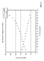
- a graph of a positive self bias of a substrate vs. gas flow is shown in FIG. 5 .
- the charge of the DC self bias can be controlled by the amount of RF power applied to substrate 116 in addition to the difference in phase. If low RF power, e.g. less than 50W, such as less than 2W, is applied to chuck 110, and the phase is locked, e.g., between 190° and 240°, such as 220°, a time-average positive DC self bias, e.g. of 10V-100V, such as 60V, can develop on substrate 116. A positive voltage results in attracting and accelerating electrons from the plasma to the surface of substrate 116. Those electrons with sufficient energies will cause modification of the sputtered material properties without causing any substantial re-sputtering due to their low momentum.
- low RF power e.g. less than 50W, such as less than 2W
- a time-average positive DC self bias e.g. of 10V-100V, such as 60V
- a positive voltage can prevent plasma ions from bombarding the surface of substrate 116 and thus avoid etching of the surface.
- a higher RF power is applied to the substrate, e.g. greater than 50W, and the phase is locked at, for example, below 190° or above 240°, such as below 180° or above 270°
- a negative DC self bias can develop on substrate 116.
- a negative voltage can cause plasma ions to be attracted and accelerated towards the substrate, which can result in re-sputtering of the surface. Re-sputtering can be useful, for example, for etching the substrate surface.
- experimentation may be required to obtain the phase shift necessary to generate a positive or negative self bias voltage.
- FIG. 6A A flow chart for a process of forming a thin film using the apparatus of FIGS. 1A and 3A is shown in FIG. 6A .
- a first radio frequency signal having a first phase is applied to a cathode in a physical vapor deposition apparatus.
- the cathode can include a sputtering target.
- a second radio frequency signal having a second phase is applied to a chuck supporting a substrate in the physical vapor deposition apparatus.
- the difference between the first and second phases creates a positive self bias DC voltage on the substrate.
- material from the sputtering target is deposited onto the substrate.
- a DC self bias can develop on the substrate.
- the capacitances of the variable tune capacitor 111 and/or the shunt capacitor 115 can be selected or adjusted, for example to between 10pF and 500pF, such that the desired DC self bias is developed on the substrate.
- the substrate can have a resulting a negative, positive, or zero charge, for example -300V to +300V, in particular -100V to +100V.
- FIG. 6B A flow chart for a process of forming a thin film using the apparatus of FIGS. 1B and 3B is shown in FIG. 6B .
- a radio frequency signal is applied to a cathode in a physical vapor deposition apparatus.
- the cathode includes a sputtering target.
- a chuck supporting a substrate in the physical vapor deposition apparatus is electrically connected to an impedance matching network.
- the impedance matching network includes at least one capacitor.
- material from the sputtering target is deposited onto the substrate.
- the process can further include selecting or adjusting a capacitance of the capacitors such that a positive self bias DC voltage is generated on the substrate.
- an RF phase shifter or an impedance matching network in a physical vapor deposition apparatus can be particularly advantageous for the creation of piezoelectric thin films, such as PZT thin films.
- use of a phase shifter 105 or an impedance matching network 107 to create an indirect bias on the substrate or deposited film is advantageous because an external DC bias cannot be directly applied to a dielectric material such as PZT.
- both the RF phase shifter 105 and impedance matching network 107 can modify the electric field strength in the dark space between substrate 116 and the intended discharge space 128, thereby changing the re-sputtering effects of the deposition process.
- directly biasing a substrate can shift the overall system voltages into an offset value to both the target and/or the substrate, it cannot modify the dark space between substrate 116 and the intended discharge space 128.
- the electrons that are attracted to the surface of the substrate can cause electron heating, which can increase the mobility of the thin films atoms. Further, the electrons on the surface can help reject plasma ions from the surface to avoid re-sputtering of the surface.
- a film having a preferable structure for example, a thin film having a (100) crystalline structure, can be formed.
- Such films sputtered on a substrate having a positive DC self bias for example a PZT film having a Perovskite PZT (100)/(200) crystal orientation, can have advantageous dielectric and piezoelectric properties, such as a dielectric constant in the range of 1000 to 1700, a high d31 coefficient, and a high break-down voltage.
- PZT thin films having a (100) crystal orientation can be used as MEMS devices, such as actuators for ink dispensing devices.
Description
- The present disclosure relates generally to radio frequency (RF) sputtering physical vapor deposition (PVD).
- Radio frequency sputtering PVD is a method for depositing a thin film on a substrate. The substrate is placed in a vacuum chamber facing a target that is connected to an RF power supply. When the RF power is initiated, a plasma is formed. Positive gas ions are pulled to the target surface, strike the target, and remove target atoms by momentum transfer. The removed target atoms then deposit on the substrate to form a thin film layer. During physical vapor deposition, it can be important to control the properties of the deposited thin film.
-
US 2003/042131 A1 describes a method and apparatus for performing PVD in a plasma region which contains a high density plasma and in which the target is bombarded with high energy ions and the substrate is bombarded with comparatively low energy ions. The apparatus comprises a target assembly wherein the area of the target is small relative to the unbiased area of the chamber, thereby maximizing DC self-bias of the target; a match network is provided for permitting application of a high frequency RF voltage to create the self-bias, the target presenting a low impedance to high frequencies; the match network is constructed to minimize harmonics of the high frequency on the target. Further it describes a substrate holder in the form of a chuck. The substrate holder is connected to a RF power generator via a matching network provided to maximize power transfer to holder. According to D1 it is possible to maintain a low DC self-bias on substrate. When the self-bias on substrate has a low level, the substrate will be subjected to low energy level bombardment by ions in the plasma. - In general, in one aspect, a method of physical vapor deposition includes applying a radio frequency signal to a cathode in a physical vapor deposition apparatus, wherein the cathode includes a sputtering target, electrically connecting a chuck in the physical vapor deposition apparatus to an impedance matching network, wherein the chuck supports a substrate, and wherein the impedance matching network includes at least one capacitor, and depositing material from the sputtering target onto the substrate.
- This and other embodiments can optionally include one or more of the following features. The method of physical vapor deposition can include adjusting a capacitance of the at least one capacitor such that a positive self bias direct current voltage is generated on the substrate. Adjusting the capacitance of the at least one capacitor can include adjusting the capacitance to have a magnitude of between 10 pF and 500 pF. The positive self bias direct current voltage can be between 10 and 100V, such as approximately 60V.
- The method of physical vapor deposition can include selecting a capacitance for the at least one capacitor such that a positive self bias direct current voltage is generated on the substrate. The capacitance can be selected to be between 10 pF and 500 pF. The positive self bias direct current voltage can be between 10 and 100V, such as approximately 60V.
- The radio frequency signal can have a radio frequency power having a magnitude of between 1000W and 5000W, such as 3000W. The target can include a dielectric material. The dielectric material can include lead zirconate titinate ("PZT"). Depositing material from the sputtering target onto the substrate can include creating a thin film having a thickness of between 2000Å and 10µm, such as between 2µm and 4µm. Depositing material from the sputtering target onto the substrate can include creating a thin film having a (100) crystalline structure.
- In general, in one aspect, a physical vapor deposition apparatus includes a vacuum chamber having side walls, a cathode inside the vacuum chamber, wherein the cathode is configured to include a sputtering target, a radio frequency power supply configured to apply a radio frequency signal to the cathode, an anode inside and electrically connected to the side walls of the vacuum chamber, an impedance matching network, and a chuck inside the vacuum chamber, wherein the chuck is configured to support a substrate and is electrically connected to the impedance matching network.
- This and other embodiments can optionally include one or more of the following features. The impedance matching network can include at least one capacitor. The impedance matching network can include an input terminal electrically connected to the chuck, a first capacitor electrically connected to ground, an inductor electrically connected between the input terminal and the first capacitor, and a second capacitor electrically connected between the input terminal and ground, the second capacitor being in parallel with the inductor and the first capacitor. The impedance matching network can include a variable tune capacitor and a shunt capacitor. The target can include a dielectric material. The dielectric material can include lead zirconate titinate ("PZT"). The cathode can include a magnetron assembly.
- Creating a positive self bias DC voltage on the substrate either by locking the difference in phase between a first radio frequency signal on the cathode and a second radio frequency signal on the substrate or by connecting an impedance network to the chuck can result in the formation of thin films having advantageous piezoelectric and dielectric properties, such as PZT thin films having a dielectric constant in the range of 1000 to 1700, a high d31 coefficient, and a high break-down voltage. Likewise, creating a negative self bias using a phase shifter or an impedance matching network can be advantageous for re-sputtering, or etching, of deposited thin films, particularly PZT thin films.
- The details of one or more embodiments are set forth in the accompanying drawings and the description below. Other features, aspects, and advantages will become apparent from the description, the drawings, and the claims.
-
-
FIG. 1A is a schematic of a cross-section of an embodiment of a physical vapor deposition apparatus including an RF phase shifter and an extended anode. -
FIG. 1B is a schematic of a cross-section of an embodiment of a physical vapor deposition apparatus including an impedance matching network and an extended anode. -
FIG. 1C is an enlarged view of the extended anode ofFIG. 1 -
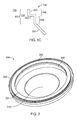
FIG. 2 shows a perspective view of an extended anode for use in a physical vapor deposition apparatus. -
FIG. 3A is a schematic of a cross-section of an embodiment of a physical vapor deposition apparatus including an RF phase shifter and an extended shield. -
FIG. 3B is a schematic of a cross-section of an embodiment of a physical vapor deposition apparatus including an impedance matching network and an extended shield. -
FIG. 3C is an enlarged view of the extended shield ofFIG. 3 -
FIG. 4 is a schematic view of the top of an extended shield for use in a physical vapor deposition apparatus. -
FIG. 5 is an example graph of self bias DC voltage vs. air flow for a chuck and a cathode. -
FIG. 6A is an example flow chart of a process for depositing a thin film on a substrate using a physical vapor deposition having a phase shifter connected between a cathode power supply and a chuck power supply. -
FIG. 6B is an example flow chart of a process for depositing a thin film on a substrate using a physical vapor deposition having an impedance matching network connected to a chuck. - Like reference numbers and designations in the various drawings indicate like elements.
- When RF physical vapor deposition, or sputtering, is used to create a thin film on a substrate, it can be difficult to control the properties of the deposited film. By altering the DC self bias of the substrate, for example by locking the phase difference between an RF signal applied to the cathode and an RF signal applied to the chuck or by electrically connecting an impedance matching network to the chuck, the properties of the film can be better controlled.
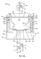
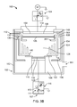
- Referring to
FIG. 1A , a physicalvapor deposition apparatus 100 can include avacuum chamber 102. Thevacuum chamber 102 can be cylindrical and haveside walls 152, atop surface 154, andbottom surface 156. Amagnetron assembly 118 can be located at the top ofvacuum chamber 102. Themagnetron assembly 118 can include a set of magnets having alternating magnetic poles. Themagnetron assembly 118 can be stationary or can rotate about an axis perpendicular to a radius ofvacuum chamber 102. The physicalvapor deposition apparatus 100 can further include anRF power supply 104 and a corresponding load matching network, which can match the impedance of thepower supply 104 to that ofvacuum chamber 102. - A
cathode assembly 106 can be housed inside and near thetop surface 154 ofvacuum chamber 102.Cathode assembly 106 can include atarget 126 that can be bonded to a metallic backing plate (not shown). Thetarget 106 can be generally circular, with anouter edge 160. The target can be made of, for example, a dielectric material such as lead zirconate titinate ("PZT").Cathode 106 can act as an electrode for RF current when RF power is applied byRF power supply 104.Cathode assembly 106 can be electrically isolated from thevacuum chamber 102 by aninsulator ring 150. - A substrate support or chuck 110 to support one or more substrates can be housed inside
vacuum chamber 102 near, but spaced above, thebottom surface 156 of thevacuum chamber 102. Thechuck 110 can include asubstrate holding mechanism 122, such as a substrate clamping plate, configured to holdsubstrate 116 such thatsubstrate 116 can be coated with a thin film during the PVD process.Substrate 116 can be, for example, a microelectromechanical system (MEMS) wafer. A temperature control (not shown) can be located on thechuck 110 to, for example, maintain the temperature ofsubstrate 116 at a prescribed temperature between 25°C and 800°C, such as 650°C to 700°C. - In one embodiment, shown in
FIG. 1A , thechuck 110 can be electrically isolated or floating from ground, and anRF power supply 120 can be electrically connected to chuck 110 (theRF power supply 120 can be connected to ground). AnRF phase shifter 105 can be connected betweenRF power supply 120 andRF power supply 104.RF power supply 104 can serve as a phase reference toRF power supply 120 whenphase shifter 105 is activated. - In another embodiment, shown in
FIG. 1B , chuck 110 can be electrically isolated or floating from ground, and animpedance matching network 107 can be electrically connected to chuck 110 (theimpedance matching network 107 can be connected to ground). No secondary RF power supply is connected to chuck 110. Theimpedance matching network 107 can include aninput terminal 109, avariable tune capacitor 111, aninductor 113, and ashunt capacitor 115. Theinput terminal 109 can be electrically connected to chuck 110. Thevariable tune capacitor 111 can be electrically connected to ground. Theinductor 113 can be electrically connected betweeninput terminal 109 andshunt capacitor 111. Theshunt capacitor 115 can be electrically connected betweeninput terminal 109 and ground and can be in parallel withinductor 113 andvariable tune capacitor 111. - An
anode 108 can also be housed insidevacuum chamber 102. Theanode 108 can provide a counterpart electrode to thecathode 106 so as to provide an RF current return path. In some embodiments, theanode 108 and thechuck 110 can be the same component. In other embodiments, however, as described herein, theanode 108 may be electrically isolated from thechuck 110 so that thechuck 110 can be floating or held at a different potential than theanode 108. The anode can be grounded, i.e., electrically connected in this context (the anode need not be actually connected to ground), to thevacuum chamber sidewalls 152. - Referring to
FIGS. 1A ,1B ,1C, and 2 , theanode 108 can have anannular body 302 and can be extended by anannular flange 304 projecting inwardly from theannular body 302. Theannular flange 304 can define an intended discharge space 128 (seeFIG. 1A ) in which plasma can be retained during the PVD process. As shown inFIGS. 1C and 2 , theannular body 302 can comprise anupper portion 306 and alower portion 308. Theupper portion 306 can be closer to thecathode 106 than thelower portion 308. The spacing 148 (seeFIGS. 1A ,1B ) between theupper portion 306 and thetop surface 154 ofvacuum chamber 102 can be configured to prevent plasma formation therebetween. - Shown in
FIG. 1C , atop portion 320 of theupper portion 306 of the anode can extend vertically, e.g., it can be a cylinder, from thetop surface 154 of the vacuum chamber. Thetop portion 320 can be parallel to and surroundedge 160 oftarget 126. Abottom portion 322 of theupper portion 306 can extend, e.g. perpendicularly, inwardly from an inside surface at the bottom edge oftop portion 320.Bottom portion 322 can extend substantially horizontally inwardly, e.g., as a horizontal ring. The inner radius of thering 322 can have approximately the same radius astarget 126.Lower portion 308 can extend from a lower surface and an inner edge ofbottom portion 322.Lower portion 308 can extend perpendicularly frombottom portion 322 and can extend vertically, e.g. as a cylinder. An inside wall of the cylinder can have approximately the same radius astarget 126. Although not shown, another projection can extend downwardly from the lower surface ofbottom portion 322 near the outside edge such that a gap is formed for the placement of an upper portion ofshield 124. - The
annular flange 304 can project inwardly from thelower portion 308 such that at least some of the flange extends belowtarget 126. As shown inFIG. 1A , theflange 304 can extend inwardly and downwardly from theannular body 302 such that the radius of theflange 304 closer to thecathode 106 is larger than the radius of theflange 304 further from thecathode 106, i.e. the flange can have a funnel shape. Alternatively, as shown inFIGS. 3A and3B , theflange 304 can extend horizontally from theannular body 302. In some embodiments, theflange 304 extends from the lowermost edge of thelower portion 308. - An annular opening 310 (see
FIG. 2 ) can have approximately the same radius as thechuck 110 such that there is no substantial shadowing of thesubstrate 116 during the PVD process, i.e. such that the entire top surface ofsubstrate 116 can be covered with a thin film. - The
vacuum chamber 102 can also include anRF shield 124 to protect the sidewalls ofvacuum chamber 102 from being coated with thin film material. Theshield 124 can be made, for example, of non-magnetic stainless steel or aluminum and can be grounded to thesidewalls 152 of thevacuum chamber 102. - In some implementations, shown in
FIGS. 1A and1B , theshield 124 can include anannular body 402 that extends vertically, e.g. in a cylindrical shape. A horizontally extendingflange 146 can extend inwardly from a bottom edge of theannular body 402. The horizontally extendingflange 146 can be located near the bottom of thevacuum chamber 102 and can extend past theflange 304 to surround and partially vertically overlap thelower portion 308 of theanode 108. In some embodiments, the vertically extendingflange 146 can extend into a gap between thelower portion 308 of theanode 108 andsubstrate holding mechanism 122. Theflange 146 can partially horizontally overlap thesubstrate holding mechanism 122. - The annular opening 406 (see
FIG. 4 ) inside theannular flange 146 of theshield 124 can have approximately the same radius as the chuck such that there is no substantial shadowing of thesubstrate 116. Agap 132 can exist between theshield 124 and theanode 108 in order to permit process gas to be evacuated from the intendeddischarge space 128. - In some embodiments, shown in
FIGS. 3A ,3B ,3C, and 4 , the shield can be extended such that a set of concentricannular projections 404 projects from theannular flange 146, for example towards thecathode 106. Theannular projections 404 can extend parallel toannular body 402. As shown inFIGS. 3A and3B , the height of theannular projections 404 can increase along a radius from the center of thevacuum chamber 102 to thesidewalls 152. Theannular body 402 can have a height that is taller than the height of theannular projections 404. - The physical
vapor deposition apparatus 102 can further include an electricallyconductive body 130, for example a strap, that directly connects theanode 108 and theshield 124. The electricallyconductive body 130 can be flexible and can be configured to permit gas flow between theanode 108 andshield 124. For example, the electricallyconductive body 130 can be a mesh or a wire strap. The electricallyconductive body 130 can be made, for example, of copper or aluminum. - There can be a number of connections between the
anode 108 andshield 124. For example, the electricallyconductive body 130 can be connected to theanode 108 and theshield 124 at at least four points. The electricallyconductive body 130 can be connected between a lower surface of theanode 108 and a top portion of theshield 124. The electricallyconductive body 130 can also be connected between a top portion of theanode 108 and an outer surface of theshield 124. - The physical
vapor deposition apparatus 100 can further include asecondary chamber shield 134. The chamber shield can be made of, for example, non-magnetic stainless steel or aluminum. An upper portion of the chamber shield can be positioned between theanode 108 and the sidewalls of thevacuum chamber 102. A lower portion of thechamber shield 134 can be positioned between the sidewalls of thevacuum chamber 102 andshield 124. Thechamber shield 134 can be concentric with andsurround shield 124 and/oranode 108. The height of thechamber shield 134 can be equal to or greater than the height ofshield 124. Thechamber shield 134 can include a verticalannular body 142 and anannular flange 144 extending inwardly from theannular body 142, e.g., from the lower edge of the verticalannular body 142. Theannular flange 144 of thechamber shield 134 can extend below theannular flange 146 ofshield 124, but can have a radial length that is shorter than theannular flange 146. Theannular flange 144 can be closer to the bottom of the chamber than thechuck 110. The inner edge of theflange 144 of the chamber shield can be vertically aligned with the outer edge of thechuck 110. - The
chamber shield 130 can be configured such that process gases may still be pumped into and out of thevacuum chamber 102. For example, thechamber shield 134 may be short enough so as not to cover thegas inlet 142 or thevacuum inlet 114. Alternatively, thechamber shield 134 may have holes (not shown) in locations corresponding to the locations ofgas inlet 142 andvacuum inlet 114. Furthermore, thechamber shield 134 can be separately removable and can be cleaned easily and reused over time. - The
chamber shield 134 can be electrically bonded to shield 124 with an electricallyconductive body 136. The electricallyconductive body 136 can be of similar material and shape as electricallyconductive body 130. Thus, the electricallyconductive body 136 can be configured to permit gas flow betweenshield 124 andchamber shield 134. Likewise, the electricallyconductive body 136 can be composed of mesh, can be one or more strap, and can comprise copper or aluminum. Moreover, the electricallyconductive body 136 can be connected between a bottom surface ofshield 124 and an inner surface ofchamber shield 134. - The physical
vapor deposition apparatus 100 can further include aprocess gas inlet 112, process gas control devices (not shown), avacuum inlet 114, pressure measurement and control devices (not shown), and vacuum pumps (not shown). - During the sputtering or PVD process, gases, such as argon and oxygen, are supplied through the
gas inlet 112 at a flow rate of 10-200 sccm/0.2 to 4sccm, such as 10 to 60 sccm/0.5 to 2 sccm. A vacuum pump (not shown) maintains a base vacuum, for example, of 10-7 Torr or below, and a plasma operation pressure, for example, of 0.5mTorr to 20mTorr, particularly 4mTorr, throughvacuum inlet 114. When the RF power fromRF power supply 104 is applied on the order of 500W to 5,000W, for example 2000W to 4,000W, or 3000W, to thecathode assembly 106, thetarget 126 is negatively biased and theanode 108 is positively biased, causing plasma to form in the intendeddischarge space 128 between thecathode 104 and theanode 108. Themagnetron assembly 118 creates a magnetic field of, for example, 50 Gauss to 400 Gauss, such as 200 Gauss to 300 Gauss, at and near the front surface of thecathode 106. The magnetic field confines the electrons to a helical motion parallel to the front surface oftarget 126. - The negative selfbias DC voltage on
target 126, in conjunction with the electrons confined near the surface oftarget 126 by the magnetic field, facilitates bombardment of thetarget 126 by energetic positive ions of the plasma. Momentum transfer causes neutral target material, such as PZT molecules, to dislocate from thetarget 126 and deposit onsubstrate 116, creating a thin film onsubstrate 116. The resulting thin film can have a thickness of 2000Å to 10µm, for example 2-4µm. - In the embodiment shown in
FIGS. 1A and3A , whenRF power supply 120 is applied tosubstrate 116, a DC self bias can develop on the substrate.RF Phase shifter 105 can be used to adjust the phases, e.g. the current or voltage phase, of the RF signal applied byRF power supply 104 and/orRF power supply 120. TheRF phase shifter 105 can lock the respective phases such that the difference in phase, e.g. from 0° to 360° creates the desired DC self bias on the substrate, which can have a negative, positive, or zero charge, for example -300V to +300V, in particular -100V to +100V. As an example, a graph of a positive self bias of a substrate vs. gas flow is shown inFIG. 5 . - The charge of the DC self bias can be controlled by the amount of RF power applied to
substrate 116 in addition to the difference in phase. If low RF power, e.g. less than 50W, such as less than 2W, is applied to chuck 110, and the phase is locked, e.g., between 190° and 240°, such as 220°, a time-average positive DC self bias, e.g. of 10V-100V, such as 60V, can develop onsubstrate 116. A positive voltage results in attracting and accelerating electrons from the plasma to the surface ofsubstrate 116. Those electrons with sufficient energies will cause modification of the sputtered material properties without causing any substantial re-sputtering due to their low momentum. Moreover, a positive voltage can prevent plasma ions from bombarding the surface ofsubstrate 116 and thus avoid etching of the surface. In contrast, if a higher RF power is applied to the substrate, e.g. greater than 50W, and the phase is locked at, for example, below 190° or above 240°, such as below 180° or above 270°, a negative DC self bias can develop onsubstrate 116. A negative voltage can cause plasma ions to be attracted and accelerated towards the substrate, which can result in re-sputtering of the surface. Re-sputtering can be useful, for example, for etching the substrate surface. For a given implementation, such as chamber configuration, gas composition and flow rate, pressure, magnetic field, and voltage, experimentation may be required to obtain the phase shift necessary to generate a positive or negative self bias voltage. - A flow chart for a process of forming a thin film using the apparatus of
FIGS. 1A and3A is shown inFIG. 6A . At 602, a first radio frequency signal having a first phase is applied to a cathode in a physical vapor deposition apparatus. The cathode can include a sputtering target. At 604, a second radio frequency signal having a second phase is applied to a chuck supporting a substrate in the physical vapor deposition apparatus. The difference between the first and second phases creates a positive self bias DC voltage on the substrate. At 606, material from the sputtering target is deposited onto the substrate. - In the embodiment shown in
FIGS. 1B and3B , whenRF power supply 104 is applied tocathode 106, and animpedance matching network 107 is connected to thechuck 110, a DC self bias can develop on the substrate. The capacitances of thevariable tune capacitor 111 and/or theshunt capacitor 115 can be selected or adjusted, for example to between 10pF and 500pF, such that the desired DC self bias is developed on the substrate. As in the embodiment described above, the substrate can have a resulting a negative, positive, or zero charge, for example -300V to +300V, in particular -100V to +100V. - A flow chart for a process of forming a thin film using the apparatus of
FIGS. 1B and3B is shown inFIG. 6B . At 610, a radio frequency signal is applied to a cathode in a physical vapor deposition apparatus. The cathode includes a sputtering target. At 612, a chuck supporting a substrate in the physical vapor deposition apparatus is electrically connected to an impedance matching network. The impedance matching network includes at least one capacitor. At 614, material from the sputtering target is deposited onto the substrate. Although not shown inFIG. 6 , the process can further include selecting or adjusting a capacitance of the capacitors such that a positive self bias DC voltage is generated on the substrate. - Use of either an RF phase shifter or an impedance matching network in a physical vapor deposition apparatus can be particularly advantageous for the creation of piezoelectric thin films, such as PZT thin films. In particular, use of a
phase shifter 105 or animpedance matching network 107 to create an indirect bias on the substrate or deposited film is advantageous because an external DC bias cannot be directly applied to a dielectric material such as PZT. Furthermore, both theRF phase shifter 105 andimpedance matching network 107 can modify the electric field strength in the dark space betweensubstrate 116 and the intendeddischarge space 128, thereby changing the re-sputtering effects of the deposition process. In contrast, while directly biasing a substrate can shift the overall system voltages into an offset value to both the target and/or the substrate, it cannot modify the dark space betweensubstrate 116 and the intendeddischarge space 128. - If PZT films are sputtered using a physical vapor deposition apparatus having a substrate with a positive DC self bias as described herein, the electrons that are attracted to the surface of the substrate can cause electron heating, which can increase the mobility of the thin films atoms. Further, the electrons on the surface can help reject plasma ions from the surface to avoid re-sputtering of the surface. As a result, a film having a preferable structure, for example, a thin film having a (100) crystalline structure, can be formed. Such films sputtered on a substrate having a positive DC self bias, for example a PZT film having a Perovskite PZT (100)/(200) crystal orientation, can have advantageous dielectric and piezoelectric properties, such as a dielectric constant in the range of 1000 to 1700, a high d31 coefficient, and a high break-down voltage. For example, PZT thin films having a (100) crystal orientation can be used as MEMS devices, such as actuators for ink dispensing devices.
- A number of embodiments have been described. Nevertheless, it will be understood that various modifications may be made of what is described. For example, it should be understood that terms of positioning and orientation (e.g., top, vertical) have been used to describe the relative positioning and orientation of components within the physical vapor deposition apparatus, but the physical vapor deposition apparatus itself can be held in a vertical or horizontal orientation or some other orientation. As another example, the steps of the exemplary flow chart of
FIGS. 6A, 6B may be performed in other orders, some steps may be removed, and other steps may be added. Accordingly, other embodiments are within the scope of the following claims.
Claims (7)
- A method of physical vapor deposition comprising:applying a radio frequency signal to a cathode in a physical vapor deposition apparatus, wherein the cathode includes a dielectric sputtering target;electrically connecting a chuck in the physical vapor deposition apparatus to an impedance matching network, wherein the chuck supports a substrate, and wherein the impedance matching network includes at least one capacitor;selecting or adjusting a capacitance of the at least one capacitor such that a positive self bias direct current voltage is generated on the substrate, wherein the positive self bias direct current voltage is between 10V and 100V; anddepositing material from the dielectric sputtering target onto the substrate.
- The method of claim 1, wherein selecting or adjusting the capacitance of the at least one capacitor comprises selecting or adjusting the capacitance to have a magnitude of between 10pF and 500pF.
- The method of claim 1, wherein the radio frequency signal has a radio frequency power having a magnitude of between 1000W and 5000W.
- The method of claim 1, wherein depositing the material from the dielectric sputtering target onto the substrate comprises creating a dielectric thin film having a thickness of between 2000Å and 10µm.
- The method of claim 4, wherein the dielectric thin film has a thickness of between 2µm and 4µm.
- The method of claim 1, wherein depositing the material from the dielectric sputtering target onto the substrate comprises creating a dielectric thin film having a (100) crystalline structure.
- The method of claim 1, wherein:the radio frequency signal applied to the cathode is a first radio frequency signal having a first phase; andthe method further comprises applying a second radio frequency signal having a second phase to the chuck, wherein a difference between the first and second phases contributes to generating the positive self bias direct current voltage on the substrate.
Applications Claiming Priority (2)
| Application Number | Priority Date | Filing Date | Title |
|---|---|---|---|
| US12/389,253 US8540851B2 (en) | 2009-02-19 | 2009-02-19 | Physical vapor deposition with impedance matching network |
| PCT/US2010/024549 WO2010096533A1 (en) | 2009-02-19 | 2010-02-18 | Physical vapor deposition with impedance matching network |
Publications (3)
| Publication Number | Publication Date |
|---|---|
| EP2398930A1 EP2398930A1 (en) | 2011-12-28 |
| EP2398930A4 EP2398930A4 (en) | 2013-07-03 |
| EP2398930B1 true EP2398930B1 (en) | 2015-06-24 |
Family
ID=42558973
Family Applications (1)
| Application Number | Title | Priority Date | Filing Date |
|---|---|---|---|
| EP10744283.2A Active EP2398930B1 (en) | 2009-02-19 | 2010-02-18 | Physical vapor deposition with impedance matching network |
Country Status (5)
| Country | Link |
|---|---|
| US (1) | US8540851B2 (en) |
| EP (1) | EP2398930B1 (en) |
| JP (1) | JP2012518722A (en) |
| KR (1) | KR101371003B1 (en) |
| WO (1) | WO2010096533A1 (en) |
Families Citing this family (11)
| Publication number | Priority date | Publication date | Assignee | Title |
|---|---|---|---|---|
| US20100206713A1 (en) * | 2009-02-19 | 2010-08-19 | Fujifilm Corporation | PZT Depositing Using Vapor Deposition |
| US8557088B2 (en) * | 2009-02-19 | 2013-10-15 | Fujifilm Corporation | Physical vapor deposition with phase shift |
| DE102011086111B4 (en) | 2011-11-10 | 2016-03-17 | Fhr Anlagenbau Gmbh | Arrangement for feeding HF current for tube cathodes |
| US20130284589A1 (en) * | 2012-04-30 | 2013-10-31 | Youming Li | Radio frequency tuned substrate biased physical vapor deposition apparatus and method of operation |
| KR102222902B1 (en) | 2014-05-12 | 2021-03-05 | 삼성전자주식회사 | Plasma apparatus and method of fabricating semiconductor device using the same |
| JP6900469B2 (en) * | 2017-05-09 | 2021-07-07 | 富士フイルム株式会社 | Film formation equipment and piezoelectric film deposition method |
| KR20210102437A (en) * | 2018-12-19 | 2021-08-19 | 에바텍 아크티엔게젤샤프트 | Vacuum system and method for depositing compound layers |
| CN112853286A (en) | 2019-11-12 | 2021-05-28 | 应用材料公司 | Physical vapor deposition of piezoelectric films |
| WO2021148195A1 (en) * | 2020-01-24 | 2021-07-29 | Evatec Ag | Phase shift controlled sputter system and process |
| CN116940705B (en) * | 2021-07-16 | 2024-03-08 | 株式会社爱发科 | Film forming method and film forming apparatus |
| WO2023286289A1 (en) * | 2021-07-16 | 2023-01-19 | 株式会社アルバック | Film formation method and film formation device |
Family Cites Families (45)
| Publication number | Priority date | Publication date | Assignee | Title |
|---|---|---|---|---|
| US3617459A (en) | 1967-09-15 | 1971-11-02 | Ibm | Rf sputtering method and apparatus for producing insulating films of varied physical properties |
| US4036723A (en) * | 1975-08-21 | 1977-07-19 | International Business Machines Corporation | RF bias sputtering method for producing insulating films free of surface irregularities |
| US4131533A (en) | 1977-12-30 | 1978-12-26 | International Business Machines Corporation | RF sputtering apparatus having floating anode shield |
| US4584079A (en) | 1983-10-11 | 1986-04-22 | Honeywell Inc. | Step shape tailoring by phase angle variation RF bias sputtering |
| JPS61276966A (en) * | 1985-04-30 | 1986-12-06 | Oki Electric Ind Co Ltd | High-frequency sputtering method for electrifiable material |
| US4622122A (en) | 1986-02-24 | 1986-11-11 | Oerlikon Buhrle U.S.A. Inc. | Planar magnetron cathode target assembly |
| JPS6459920A (en) * | 1987-08-31 | 1989-03-07 | Hitachi Ltd | Device for forming thin film |
| JPH03201713A (en) | 1989-12-28 | 1991-09-03 | Clarion Co Ltd | Piezoelectric film manufacturing instrument |
| US5198090A (en) | 1990-08-31 | 1993-03-30 | International Business Machines Corporation | Sputtering apparatus for producing thin films of material |
| JP2635267B2 (en) * | 1991-06-27 | 1997-07-30 | アプライド マテリアルズ インコーポレイテッド | RF plasma processing equipment |
| JP3441746B2 (en) | 1992-11-09 | 2003-09-02 | キヤノン株式会社 | Bias sputtering method and apparatus |
| JPH0715051A (en) * | 1993-06-24 | 1995-01-17 | Mitsubishi Electric Corp | Manufacture of ybco superconducting thin film |
| JP3490483B2 (en) | 1993-10-08 | 2004-01-26 | アネルバ株式会社 | Method for producing PZT thin film |
| EP0692156A1 (en) * | 1994-01-31 | 1996-01-17 | Applied Materials, Inc. | Electrostatic chuck with conformal insulator film |
| US5729423A (en) | 1994-01-31 | 1998-03-17 | Applied Materials, Inc. | Puncture resistant electrostatic chuck |
| JP3890634B2 (en) * | 1995-09-19 | 2007-03-07 | セイコーエプソン株式会社 | Piezoelectric thin film element and ink jet recording head |
| JPH09176850A (en) | 1995-12-22 | 1997-07-08 | Ulvac Japan Ltd | Sputtering device and production of dielectric film |
| US6579426B1 (en) * | 1997-05-16 | 2003-06-17 | Applied Materials, Inc. | Use of variable impedance to control coil sputter distribution |
| US5910886A (en) | 1997-11-07 | 1999-06-08 | Sierra Applied Sciences, Inc. | Phase-shift power supply |
| TW584905B (en) | 2000-02-25 | 2004-04-21 | Tokyo Electron Ltd | Method and apparatus for depositing films |
| JP3944341B2 (en) | 2000-03-28 | 2007-07-11 | 株式会社東芝 | Manufacturing method of oxide epitaxial strained lattice film |
| US6440280B1 (en) | 2000-06-28 | 2002-08-27 | Sola International, Inc. | Multi-anode device and methods for sputter deposition |
| US6471830B1 (en) | 2000-10-03 | 2002-10-29 | Veeco/Cvc, Inc. | Inductively-coupled-plasma ionized physical-vapor deposition apparatus, method and system |
| JP4553476B2 (en) | 2000-10-24 | 2010-09-29 | 株式会社アルバック | Sputtering method and sputtering apparatus |
| JP2003166047A (en) * | 2001-09-20 | 2003-06-13 | Shin Meiwa Ind Co Ltd | Method and apparatus for forming film of halogen compound, and magnesium fluoride film |
| JP4204824B2 (en) | 2001-09-20 | 2009-01-07 | 新明和工業株式会社 | Optical system |
| US20030180450A1 (en) | 2002-03-22 | 2003-09-25 | Kidd Jerry D. | System and method for preventing breaker failure |
| WO2003083911A1 (en) | 2002-03-28 | 2003-10-09 | Tokyo Electron Limited | A system and method for determining the state of a film in a plasma reactor using an electrical property |
| SE526857C2 (en) | 2003-12-22 | 2005-11-08 | Seco Tools Ab | Ways of coating a cutting tool using reactive magnetron sputtering |
| US7820020B2 (en) | 2005-02-03 | 2010-10-26 | Applied Materials, Inc. | Apparatus for plasma-enhanced physical vapor deposition of copper with RF source power applied through the workpiece with a lighter-than-copper carrier gas |
| JP4851108B2 (en) | 2005-03-24 | 2012-01-11 | 富士フイルム株式会社 | Method for forming film of composite perovskite compound and method for manufacturing liquid discharge head using the same |
| JP5063892B2 (en) | 2005-12-20 | 2012-10-31 | 富士フイルム株式会社 | Method for manufacturing liquid discharge head |
| US7837838B2 (en) | 2006-03-09 | 2010-11-23 | Applied Materials, Inc. | Method of fabricating a high dielectric constant transistor gate using a low energy plasma apparatus |
| CN101401194B (en) * | 2006-03-09 | 2011-12-28 | 应用材料股份有限公司 | Method and apparatus for fabricating a high dielectric constant transistor gate using a low energy plasma system |
| US20080083611A1 (en) * | 2006-10-06 | 2008-04-10 | Tegal Corporation | High-adhesive backside metallization |
| JP5194463B2 (en) * | 2007-01-31 | 2013-05-08 | パナソニック株式会社 | Method for manufacturing piezoelectric thin film element |
| US8020974B2 (en) | 2007-01-31 | 2011-09-20 | Panasonic Corporation | Piezoelectric thin film device and piezoelectric thin film device manufacturing method, and inkjet head and inkjet recording apparatus |
| EP1973177B8 (en) | 2007-03-22 | 2015-01-21 | FUJIFILM Corporation | Ferroelectric film, process for producing the same, ferroelectric device, and liquid discharge device |
| JP2008266771A (en) * | 2007-03-22 | 2008-11-06 | Fujifilm Corp | Ferroelectric film, process for producing the same, ferroelectric device, and liquid discharge device |
| JP4903610B2 (en) | 2007-03-27 | 2012-03-28 | 東京エレクトロン株式会社 | Plasma processing equipment |
| JP4317888B2 (en) | 2007-08-31 | 2009-08-19 | 富士フイルム株式会社 | Sputtering method and sputtering apparatus |
| US8043487B2 (en) | 2008-12-12 | 2011-10-25 | Fujifilm Corporation | Chamber shield for vacuum physical vapor deposition |
| US8066857B2 (en) | 2008-12-12 | 2011-11-29 | Fujifilm Corporation | Shaped anode and anode-shield connection for vacuum physical vapor deposition |
| US8557088B2 (en) | 2009-02-19 | 2013-10-15 | Fujifilm Corporation | Physical vapor deposition with phase shift |
| US20100206713A1 (en) | 2009-02-19 | 2010-08-19 | Fujifilm Corporation | PZT Depositing Using Vapor Deposition |
-
2009
- 2009-02-19 US US12/389,253 patent/US8540851B2/en active Active
-
2010
- 2010-02-18 JP JP2011551211A patent/JP2012518722A/en not_active Abandoned
- 2010-02-18 KR KR1020117021524A patent/KR101371003B1/en active IP Right Grant
- 2010-02-18 WO PCT/US2010/024549 patent/WO2010096533A1/en active Application Filing
- 2010-02-18 EP EP10744283.2A patent/EP2398930B1/en active Active
Also Published As
| Publication number | Publication date |
|---|---|
| KR101371003B1 (en) | 2014-03-10 |
| EP2398930A4 (en) | 2013-07-03 |
| EP2398930A1 (en) | 2011-12-28 |
| US20100206718A1 (en) | 2010-08-19 |
| JP2012518722A (en) | 2012-08-16 |
| US8540851B2 (en) | 2013-09-24 |
| WO2010096533A1 (en) | 2010-08-26 |
| KR20110120323A (en) | 2011-11-03 |
Similar Documents
| Publication | Publication Date | Title |
|---|---|---|
| EP2398930B1 (en) | Physical vapor deposition with impedance matching network | |
| US8133362B2 (en) | Physical vapor deposition with multi-point clamp | |
| US8043487B2 (en) | Chamber shield for vacuum physical vapor deposition | |
| US8066857B2 (en) | Shaped anode and anode-shield connection for vacuum physical vapor deposition | |
| US6358376B1 (en) | Biased shield in a magnetron sputter reactor | |
| US9181619B2 (en) | Physical vapor deposition with heat diffuser | |
| US20090308732A1 (en) | Apparatus and method for uniform deposition | |
| US8557088B2 (en) | Physical vapor deposition with phase shift | |
| US7517437B2 (en) | RF powered target for increasing deposition uniformity in sputtering systems | |
| CN106011761B (en) | Method and apparatus for depositing material | |
| CN106574363B (en) | Low heteropical method and apparatus is maintained during the target lifetime | |
| EP2660351B1 (en) | Radio frequency tuned substrate biased physical vapor deposition apparatus and method of operation | |
| US20110209989A1 (en) | Physical vapor deposition with insulated clamp | |
| US20140110248A1 (en) | Chamber pasting method in a pvd chamber for reactive re-sputtering dielectric material |
Legal Events
| Date | Code | Title | Description |
|---|---|---|---|
| PUAI | Public reference made under article 153(3) epc to a published international application that has entered the european phase |
Free format text: ORIGINAL CODE: 0009012 |
|
| 17P | Request for examination filed |
Effective date: 20110907 |
|
| AK | Designated contracting states |
Kind code of ref document: A1 Designated state(s): AT BE BG CH CY CZ DE DK EE ES FI FR GB GR HR HU IE IS IT LI LT LU LV MC MK MT NL NO PL PT RO SE SI SK SM TR |
|
| DAX | Request for extension of the european patent (deleted) | ||
| RIN1 | Information on inventor provided before grant (corrected) |
Inventor name: BIRKMEYER, JEFFREY Inventor name: NAONO, TAKAYUKI Inventor name: FUJII, TAKAMICHI Inventor name: HISHINUMA, YOSHIKAZU Inventor name: LI, YOUMING |
|
| A4 | Supplementary search report drawn up and despatched |
Effective date: 20130604 |
|
| RIC1 | Information provided on ipc code assigned before grant |
Ipc: C23C 14/00 20060101AFI20130528BHEP Ipc: C23C 14/34 20060101ALI20130528BHEP |
|
| 17Q | First examination report despatched |
Effective date: 20131114 |
|
| GRAP | Despatch of communication of intention to grant a patent |
Free format text: ORIGINAL CODE: EPIDOSNIGR1 |
|
| RIC1 | Information provided on ipc code assigned before grant |
Ipc: C23C 14/00 20060101AFI20150113BHEP Ipc: C23C 14/34 20060101ALI20150113BHEP Ipc: H01J 37/34 20060101ALI20150113BHEP |
|
| INTG | Intention to grant announced |
Effective date: 20150211 |
|
| GRAS | Grant fee paid |
Free format text: ORIGINAL CODE: EPIDOSNIGR3 |
|
| GRAA | (expected) grant |
Free format text: ORIGINAL CODE: 0009210 |
|
| AK | Designated contracting states |
Kind code of ref document: B1 Designated state(s): AT BE BG CH CY CZ DE DK EE ES FI FR GB GR HR HU IE IS IT LI LT LU LV MC MK MT NL NO PL PT RO SE SI SK SM TR |
|
| REG | Reference to a national code |
Ref country code: GB Ref legal event code: FG4D |
|
| REG | Reference to a national code |
Ref country code: CH Ref legal event code: EP |
|
| REG | Reference to a national code |
Ref country code: AT Ref legal event code: REF Ref document number: 732921 Country of ref document: AT Kind code of ref document: T Effective date: 20150715 |
|
| REG | Reference to a national code |
Ref country code: IE Ref legal event code: FG4D |
|
| REG | Reference to a national code |
Ref country code: DE Ref legal event code: R096 Ref document number: 602010025432 Country of ref document: DE |
|
| PG25 | Lapsed in a contracting state [announced via postgrant information from national office to epo] |
Ref country code: LT Free format text: LAPSE BECAUSE OF FAILURE TO SUBMIT A TRANSLATION OF THE DESCRIPTION OR TO PAY THE FEE WITHIN THE PRESCRIBED TIME-LIMIT Effective date: 20150624 Ref country code: HR Free format text: LAPSE BECAUSE OF FAILURE TO SUBMIT A TRANSLATION OF THE DESCRIPTION OR TO PAY THE FEE WITHIN THE PRESCRIBED TIME-LIMIT Effective date: 20150624 Ref country code: NO Free format text: LAPSE BECAUSE OF FAILURE TO SUBMIT A TRANSLATION OF THE DESCRIPTION OR TO PAY THE FEE WITHIN THE PRESCRIBED TIME-LIMIT Effective date: 20150924 Ref country code: FI Free format text: LAPSE BECAUSE OF FAILURE TO SUBMIT A TRANSLATION OF THE DESCRIPTION OR TO PAY THE FEE WITHIN THE PRESCRIBED TIME-LIMIT Effective date: 20150624 |
|
| REG | Reference to a national code |
Ref country code: AT Ref legal event code: MK05 Ref document number: 732921 Country of ref document: AT Kind code of ref document: T Effective date: 20150624 |
|
| REG | Reference to a national code |
Ref country code: LT Ref legal event code: MG4D |
|
| PG25 | Lapsed in a contracting state [announced via postgrant information from national office to epo] |
Ref country code: BG Free format text: LAPSE BECAUSE OF FAILURE TO SUBMIT A TRANSLATION OF THE DESCRIPTION OR TO PAY THE FEE WITHIN THE PRESCRIBED TIME-LIMIT Effective date: 20150924 Ref country code: LV Free format text: LAPSE BECAUSE OF FAILURE TO SUBMIT A TRANSLATION OF THE DESCRIPTION OR TO PAY THE FEE WITHIN THE PRESCRIBED TIME-LIMIT Effective date: 20150624 Ref country code: GR Free format text: LAPSE BECAUSE OF FAILURE TO SUBMIT A TRANSLATION OF THE DESCRIPTION OR TO PAY THE FEE WITHIN THE PRESCRIBED TIME-LIMIT Effective date: 20150925 |
|
| REG | Reference to a national code |
Ref country code: NL Ref legal event code: MP Effective date: 20150624 |
|
| REG | Reference to a national code |
Ref country code: FR Ref legal event code: PLFP Year of fee payment: 7 |
|
| PG25 | Lapsed in a contracting state [announced via postgrant information from national office to epo] |
Ref country code: EE Free format text: LAPSE BECAUSE OF FAILURE TO SUBMIT A TRANSLATION OF THE DESCRIPTION OR TO PAY THE FEE WITHIN THE PRESCRIBED TIME-LIMIT Effective date: 20150624 |
|
| PG25 | Lapsed in a contracting state [announced via postgrant information from national office to epo] |
Ref country code: PL Free format text: LAPSE BECAUSE OF FAILURE TO SUBMIT A TRANSLATION OF THE DESCRIPTION OR TO PAY THE FEE WITHIN THE PRESCRIBED TIME-LIMIT Effective date: 20150624 Ref country code: CZ Free format text: LAPSE BECAUSE OF FAILURE TO SUBMIT A TRANSLATION OF THE DESCRIPTION OR TO PAY THE FEE WITHIN THE PRESCRIBED TIME-LIMIT Effective date: 20150624 Ref country code: AT Free format text: LAPSE BECAUSE OF FAILURE TO SUBMIT A TRANSLATION OF THE DESCRIPTION OR TO PAY THE FEE WITHIN THE PRESCRIBED TIME-LIMIT Effective date: 20150624 Ref country code: IS Free format text: LAPSE BECAUSE OF FAILURE TO SUBMIT A TRANSLATION OF THE DESCRIPTION OR TO PAY THE FEE WITHIN THE PRESCRIBED TIME-LIMIT Effective date: 20151024 Ref country code: RO Free format text: LAPSE BECAUSE OF NON-PAYMENT OF DUE FEES Effective date: 20150624 Ref country code: PT Free format text: LAPSE BECAUSE OF FAILURE TO SUBMIT A TRANSLATION OF THE DESCRIPTION OR TO PAY THE FEE WITHIN THE PRESCRIBED TIME-LIMIT Effective date: 20151026 Ref country code: SK Free format text: LAPSE BECAUSE OF FAILURE TO SUBMIT A TRANSLATION OF THE DESCRIPTION OR TO PAY THE FEE WITHIN THE PRESCRIBED TIME-LIMIT Effective date: 20150624 Ref country code: ES Free format text: LAPSE BECAUSE OF FAILURE TO SUBMIT A TRANSLATION OF THE DESCRIPTION OR TO PAY THE FEE WITHIN THE PRESCRIBED TIME-LIMIT Effective date: 20150624 |
|
| REG | Reference to a national code |
Ref country code: DE Ref legal event code: R097 Ref document number: 602010025432 Country of ref document: DE |
|
| PG25 | Lapsed in a contracting state [announced via postgrant information from national office to epo] |
Ref country code: IT Free format text: LAPSE BECAUSE OF FAILURE TO SUBMIT A TRANSLATION OF THE DESCRIPTION OR TO PAY THE FEE WITHIN THE PRESCRIBED TIME-LIMIT Effective date: 20150624 Ref country code: DK Free format text: LAPSE BECAUSE OF FAILURE TO SUBMIT A TRANSLATION OF THE DESCRIPTION OR TO PAY THE FEE WITHIN THE PRESCRIBED TIME-LIMIT Effective date: 20150624 |
|
| PLBE | No opposition filed within time limit |
Free format text: ORIGINAL CODE: 0009261 |
|
| STAA | Information on the status of an ep patent application or granted ep patent |
Free format text: STATUS: NO OPPOSITION FILED WITHIN TIME LIMIT |
|
| PG25 | Lapsed in a contracting state [announced via postgrant information from national office to epo] |
Ref country code: BE Free format text: LAPSE BECAUSE OF NON-PAYMENT OF DUE FEES Effective date: 20160229 |
|
| 26N | No opposition filed |
Effective date: 20160329 |
|
| PG25 | Lapsed in a contracting state [announced via postgrant information from national office to epo] |
Ref country code: SI Free format text: LAPSE BECAUSE OF FAILURE TO SUBMIT A TRANSLATION OF THE DESCRIPTION OR TO PAY THE FEE WITHIN THE PRESCRIBED TIME-LIMIT Effective date: 20150624 |
|
| PG25 | Lapsed in a contracting state [announced via postgrant information from national office to epo] |
Ref country code: LU Free format text: LAPSE BECAUSE OF FAILURE TO SUBMIT A TRANSLATION OF THE DESCRIPTION OR TO PAY THE FEE WITHIN THE PRESCRIBED TIME-LIMIT Effective date: 20160218 Ref country code: MC Free format text: LAPSE BECAUSE OF FAILURE TO SUBMIT A TRANSLATION OF THE DESCRIPTION OR TO PAY THE FEE WITHIN THE PRESCRIBED TIME-LIMIT Effective date: 20150624 |
|
| REG | Reference to a national code |
Ref country code: CH Ref legal event code: PL |
|
| PG25 | Lapsed in a contracting state [announced via postgrant information from national office to epo] |
Ref country code: LI Free format text: LAPSE BECAUSE OF NON-PAYMENT OF DUE FEES Effective date: 20160229 Ref country code: CH Free format text: LAPSE BECAUSE OF NON-PAYMENT OF DUE FEES Effective date: 20160229 |
|
| REG | Reference to a national code |
Ref country code: IE Ref legal event code: MM4A |
|
| PG25 | Lapsed in a contracting state [announced via postgrant information from national office to epo] |
Ref country code: BE Free format text: LAPSE BECAUSE OF FAILURE TO SUBMIT A TRANSLATION OF THE DESCRIPTION OR TO PAY THE FEE WITHIN THE PRESCRIBED TIME-LIMIT Effective date: 20150624 |
|
| REG | Reference to a national code |
Ref country code: FR Ref legal event code: PLFP Year of fee payment: 8 |
|
| PG25 | Lapsed in a contracting state [announced via postgrant information from national office to epo] |
Ref country code: IE Free format text: LAPSE BECAUSE OF NON-PAYMENT OF DUE FEES Effective date: 20160218 |
|
| PG25 | Lapsed in a contracting state [announced via postgrant information from national office to epo] |
Ref country code: NL Free format text: LAPSE BECAUSE OF FAILURE TO SUBMIT A TRANSLATION OF THE DESCRIPTION OR TO PAY THE FEE WITHIN THE PRESCRIBED TIME-LIMIT Effective date: 20150624 Ref country code: SE Free format text: LAPSE BECAUSE OF FAILURE TO SUBMIT A TRANSLATION OF THE DESCRIPTION OR TO PAY THE FEE WITHIN THE PRESCRIBED TIME-LIMIT Effective date: 20150624 |
|
| PG25 | Lapsed in a contracting state [announced via postgrant information from national office to epo] |
Ref country code: MT Free format text: LAPSE BECAUSE OF FAILURE TO SUBMIT A TRANSLATION OF THE DESCRIPTION OR TO PAY THE FEE WITHIN THE PRESCRIBED TIME-LIMIT Effective date: 20150624 |
|
| REG | Reference to a national code |
Ref country code: FR Ref legal event code: PLFP Year of fee payment: 9 |
|
| PG25 | Lapsed in a contracting state [announced via postgrant information from national office to epo] |
Ref country code: SM Free format text: LAPSE BECAUSE OF FAILURE TO SUBMIT A TRANSLATION OF THE DESCRIPTION OR TO PAY THE FEE WITHIN THE PRESCRIBED TIME-LIMIT Effective date: 20150624 Ref country code: HU Free format text: LAPSE BECAUSE OF FAILURE TO SUBMIT A TRANSLATION OF THE DESCRIPTION OR TO PAY THE FEE WITHIN THE PRESCRIBED TIME-LIMIT; INVALID AB INITIO Effective date: 20100218 Ref country code: CY Free format text: LAPSE BECAUSE OF FAILURE TO SUBMIT A TRANSLATION OF THE DESCRIPTION OR TO PAY THE FEE WITHIN THE PRESCRIBED TIME-LIMIT Effective date: 20150624 |
|
| PG25 | Lapsed in a contracting state [announced via postgrant information from national office to epo] |
Ref country code: MT Free format text: LAPSE BECAUSE OF FAILURE TO SUBMIT A TRANSLATION OF THE DESCRIPTION OR TO PAY THE FEE WITHIN THE PRESCRIBED TIME-LIMIT Effective date: 20160229 Ref country code: MK Free format text: LAPSE BECAUSE OF FAILURE TO SUBMIT A TRANSLATION OF THE DESCRIPTION OR TO PAY THE FEE WITHIN THE PRESCRIBED TIME-LIMIT Effective date: 20150624 Ref country code: TR Free format text: LAPSE BECAUSE OF FAILURE TO SUBMIT A TRANSLATION OF THE DESCRIPTION OR TO PAY THE FEE WITHIN THE PRESCRIBED TIME-LIMIT Effective date: 20150624 |
|
| PGFP | Annual fee paid to national office [announced via postgrant information from national office to epo] |
Ref country code: GB Payment date: 20221230 Year of fee payment: 14 |
|
| PGFP | Annual fee paid to national office [announced via postgrant information from national office to epo] |
Ref country code: FR Payment date: 20230110 Year of fee payment: 14 |
|
| PGFP | Annual fee paid to national office [announced via postgrant information from national office to epo] |
Ref country code: DE Payment date: 20221229 Year of fee payment: 14 |
|
| P01 | Opt-out of the competence of the unified patent court (upc) registered |
Effective date: 20230515 |