EP2398147B1 - Verfahren sowie elektrische Schaltung zum Betreiben eines elektrischen Leistungshalbleiter-Bauelements - Google Patents
Verfahren sowie elektrische Schaltung zum Betreiben eines elektrischen Leistungshalbleiter-Bauelements Download PDFInfo
- Publication number
- EP2398147B1 EP2398147B1 EP11162816.0A EP11162816A EP2398147B1 EP 2398147 B1 EP2398147 B1 EP 2398147B1 EP 11162816 A EP11162816 A EP 11162816A EP 2398147 B1 EP2398147 B1 EP 2398147B1
- Authority
- EP
- European Patent Office
- Prior art keywords
- programming
- signals
- power semiconductor
- logic
- semiconductor element
- Prior art date
- Legal status (The legal status is an assumption and is not a legal conclusion. Google has not performed a legal analysis and makes no representation as to the accuracy of the status listed.)
- Active
Links
Images
Classifications
-
- H—ELECTRICITY
- H03—ELECTRONIC CIRCUITRY
- H03K—PULSE TECHNIQUE
- H03K17/00—Electronic switching or gating, i.e. not by contact-making and –breaking
- H03K17/51—Electronic switching or gating, i.e. not by contact-making and –breaking characterised by the components used
- H03K17/56—Electronic switching or gating, i.e. not by contact-making and –breaking characterised by the components used by the use, as active elements, of semiconductor devices
- H03K17/567—Circuits characterised by the use of more than one type of semiconductor device, e.g. BIMOS, composite devices such as IGBT
-
- H—ELECTRICITY
- H01—ELECTRIC ELEMENTS
- H01H—ELECTRIC SWITCHES; RELAYS; SELECTORS; EMERGENCY PROTECTIVE DEVICES
- H01H85/00—Protective devices in which the current flows through a part of fusible material and this current is interrupted by displacement of the fusible material when this current becomes excessive
- H01H85/02—Details
- H01H85/04—Fuses, i.e. expendable parts of the protective device, e.g. cartridges
- H01H85/041—Fuses, i.e. expendable parts of the protective device, e.g. cartridges characterised by the type
- H01H85/0411—Miniature fuses
- H01H85/0415—Miniature fuses cartridge type
- H01H85/0417—Miniature fuses cartridge type with parallel side contacts
-
- H—ELECTRICITY
- H01—ELECTRIC ELEMENTS
- H01H—ELECTRIC SWITCHES; RELAYS; SELECTORS; EMERGENCY PROTECTIVE DEVICES
- H01H85/00—Protective devices in which the current flows through a part of fusible material and this current is interrupted by displacement of the fusible material when this current becomes excessive
- H01H85/54—Protective devices wherein the fuse is carried, held, or retained by an intermediate or auxiliary part removable from the base, or used as sectionalisers
- H01H85/547—Protective devices wherein the fuse is carried, held, or retained by an intermediate or auxiliary part removable from the base, or used as sectionalisers with sliding fuse carrier
-
- H—ELECTRICITY
- H03—ELECTRONIC CIRCUITRY
- H03F—AMPLIFIERS
- H03F3/00—Amplifiers with only discharge tubes or only semiconductor devices as amplifying elements
- H03F3/04—Amplifiers with only discharge tubes or only semiconductor devices as amplifying elements with semiconductor devices only
- H03F3/08—Amplifiers with only discharge tubes or only semiconductor devices as amplifying elements with semiconductor devices only controlled by light
- H03F3/087—Amplifiers with only discharge tubes or only semiconductor devices as amplifying elements with semiconductor devices only controlled by light with IC amplifier blocks
-
- H—ELECTRICITY
- H03—ELECTRONIC CIRCUITRY
- H03K—PULSE TECHNIQUE
- H03K17/00—Electronic switching or gating, i.e. not by contact-making and –breaking
- H03K17/51—Electronic switching or gating, i.e. not by contact-making and –breaking characterised by the components used
- H03K17/56—Electronic switching or gating, i.e. not by contact-making and –breaking characterised by the components used by the use, as active elements, of semiconductor devices
- H03K17/687—Electronic switching or gating, i.e. not by contact-making and –breaking characterised by the components used by the use, as active elements, of semiconductor devices the devices being field-effect transistors
- H03K17/6877—Electronic switching or gating, i.e. not by contact-making and –breaking characterised by the components used by the use, as active elements, of semiconductor devices the devices being field-effect transistors the control circuit comprising active elements different from those used in the output circuit
-
- H—ELECTRICITY
- H03—ELECTRONIC CIRCUITRY
- H03K—PULSE TECHNIQUE
- H03K19/00—Logic circuits, i.e. having at least two inputs acting on one output; Inverting circuits
- H03K19/02—Logic circuits, i.e. having at least two inputs acting on one output; Inverting circuits using specified components
- H03K19/173—Logic circuits, i.e. having at least two inputs acting on one output; Inverting circuits using specified components using elementary logic circuits as components
- H03K19/1731—Optimisation thereof
- H03K19/1732—Optimisation thereof by limitation or reduction of the pin/gate ratio
-
- H—ELECTRICITY
- H03—ELECTRONIC CIRCUITRY
- H03K—PULSE TECHNIQUE
- H03K19/00—Logic circuits, i.e. having at least two inputs acting on one output; Inverting circuits
- H03K19/02—Logic circuits, i.e. having at least two inputs acting on one output; Inverting circuits using specified components
- H03K19/173—Logic circuits, i.e. having at least two inputs acting on one output; Inverting circuits using specified components using elementary logic circuits as components
- H03K19/177—Logic circuits, i.e. having at least two inputs acting on one output; Inverting circuits using specified components using elementary logic circuits as components arranged in matrix form
Definitions
- the invention relates to a method and an electrical circuit for operating an electrical power semiconductor component.
- the object of the invention is to provide a method and an electrical circuit for operating an electric power semiconductor device with which, for example, a program update with less effort can be transferred to the programmable logic.
- the power semiconductor device is associated with a power amplifier with a programmable logic.
- the output stage is sent drive signals for the power semiconductor device and the power semiconductor device is influenced by the output stage in response to the drive signals.
- the manner of influencing the power semiconductor device is defined by the programming of the logic.
- the output stage is sent programming signals, which are processed by a processor of the power amplifier.
- the programming of the logic is changed by the processor in dependence on the programming signals.
- This approach has the advantage that a program update according to the invention can thereby be transferred to the programmable logic of the power amplifier, that the corresponding programming signals are transmitted to the power amplifier and the local processor then reprogrammed or reprogrammed the logic according to the programming signals. It is thus no longer necessary for the service technician to act directly at the location of the power semiconductor component or the final stage. Instead, it is sufficient that the programming signals are somehow sent to the final stage. There, the programming signals are automatically processed for new or reprogramming the logic.
- the logic is switched by the processor into a programming mode, in which the power semiconductor component is no longer influenced as a function of the drive signals. This avoids that any malfunction of the power amplifier occur during the programming of the logic.
- a further advantageous embodiment of the invention is that the programming signals are sent by a controller. This makes it possible to reprogram several output stages of different power semiconductor components in the inventive manner from a central control. This is equivalent to the fact that the service technician no longer needs to individually update each power amplifier, but it is instead possible that the central controller automatically transmits the new programming to all power amplifiers. Obviously, this achieves a further substantial simplification.
- the advantages of the invention come in particular in a power converter circuit having a plurality of Power semiconductor components with associated power amplifiers to advantage.
- the invention allows only the controller to be told which programming signals to be transmitted to the plurality of power amplifiers, and that then the controller transmits these programming signals automatically to all power amplifiers, without the need for further manual effort is required.
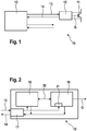
- an electrical circuit 10 in which an electric power semiconductor component 11 is driven by an output stage 12.
- the power semiconductor device 11 may be an insulated gate bipolar transistor (IGBT) or a gate turn-off (GTO) thyristor or the like.
- IGBT insulated gate bipolar transistor
- GTO gate turn-off
- Example becomes in the FIG. 1 the gate G of the power semiconductor device 11 is acted upon by the output stage and further the collector and the emitter are connected to the output stage 12. It is understood that this control can also be designed differently.
- the output stage 12 is in turn connected via two optical waveguides 13, 14 to a controller 15.
- the two optical waveguides 13, 14 are intended to transmit signals in opposite directions. It is understood that instead of the optical waveguides 13, 14, other potential-separating transmission media or transmission types are conceivable, for example via optocouplers or magnetic transmitters or by means of wireless transmissions or the like. It may also be possible to send and receive the electrical signals in both transmission directions via a single transmission medium.
- controller 15 may be provided to be connected via further optical fibers with other amplifiers and thus with other power semiconductor devices.
- the output stage 12 has a transmitter / receiver 17, to which the two optical waveguides 13, 14 are connected, and which is intended to receive via the optical waveguide 13 incoming light signals and to send on the optical waveguide 14 light signals.
- the transmitter / receiver 17 is connected to a programmable logic 18 and to a processor 19.
- a programmable logic 18 is connected to a programmable logic 18 and to a processor 19.
- FIG. 2 These connections are shown by way of example as simple forward and return lines. It is understood that insofar as other connection options are conceivable, for example, parallel or serial bus structures or the like.
- the logic 18 is provided with an output, with which the gate G of the power semiconductor device 11 is driven. Furthermore, the logic 18 and the processor 19 are connected to each other via a bidirectional line 20. It is understood that this line 20 may be any type of connection, in particular a parallel or serial bus structure.
- the processor 19 may be a conventional microprocessor or signal processor or the like.
- drive signals are sent from the controller 15 via the optical waveguide 13 to the output stage 12. These drive signals are also referred to as "firing pulses FP".
- the drive signals are received by the transmitter / receiver 17 of the power amplifier 12 and processed by the logic 18. From the logic 18, the power semiconductor device 11 is then turned on or off in response to the individual drive signals via its gate G or on or off.
- the drive signals are usually defined signals with predetermined pulse durations and amplitudes. Based on these specifications, the logic 18 can recognize the drive signals and distinguish them from other signals. For this purpose, an upstream filter 21 may be present in the logic 18, from which only the drive signals are passed on for further processing. For example, it is possible that the drive signals have a longer pulse duration, and that the filter 21 does not pass other signals with short signal durations.
- the output stage 12 can detect the switching operations of the power semiconductor component 11 in a manner not shown.
- the transmitter / receiver 17 of the output stage 12 can send a so-called “indication pulse IP" via the optical waveguide 14 to the controller 15.
- the controller 15 can conclude the functionality or a malfunction of the power semiconductor component 11.
- the drive signals are also received by the processor 19, but not further processed.
- programming signals are sent to the output stage 12 via the optical waveguide 13 by the controller 10.
- the programming signals are received by the transceiver 17 and forwarded to the logic 18 and the processor 19.
- the programming signals differ in particular with regard to their signal duration and / or amplitude from the drive signals. For example, it is possible that the programming signals have a shorter signal duration.
- the programming signals are therefore filtered out by the filter 21 and not passed on to the logic 18.
- the programming signals are thus not processed by the logic 18 for the purpose of driving the power semiconductor device 11. However, the programming signals are processed by the processor 19.
- the processor 19 can recognize and further process the programming signals transmitted by the control unit as such.
- the transmitted programming signals contain at their beginning in time a start coding, with which the processor 19 is informed that now follow the actual programming signals.
- the logic 18 is switched by the processor 19 via the line 20 from the normal mode to the programming mode. This means that the power semiconductor device 11 is no longer driven by the logic 18 and no other, related to the power semiconductor device 11 functions more of the logic 18 are executed.
- the received programming signals are conditioned by the processor 19 so that the logic 18 can now be programmed with these programming signals.
- JTAG joint test action group.
- FPGAs or CPLDs can be programmed using the JTAG protocol.
- the processed programming signals are passed from the processor 19 via the line 20 to the logic 18.
- the received programming signals are acknowledged by the logic 18 via the same line 20 to the processor 19.
- the logic 18 becomes a function of the programming signals new functionality given. So there is a programming of the logic 18 via the line 20 based on the processed programming signals.
- the end of the programming can be communicated to the processor 19 either by terminating the transmission of the programming signals or by an end coding last transmitted by the control unit 15.
- the logic 18 is switched back from the processor 19 via the line 20 from the programming mode back to the normal mode.
- the end of the programming operation or the return to normal operation can be reported by the processor 19 via the transmitter / receiver 17 to the controller 15.
- a reset signal or the like from the controller 15 is required.
- the logic 18 of the output stage 12 can be reprogrammed.
- other output stages of power semiconductor components can be programmed in a corresponding manner. Overall, it is thus possible, for example, to program all output stages of the power semiconductor components of a converter circuit.
- controller 15 is provided to influence all output stages of the power semiconductor components of an entire power converter circuit, so can from this Control 15 all power amplifiers can also be programmed. If the controller 15 is additionally provided to cooperate with a so-called remote maintenance, it is possible to program the output stages of the converter circuit via this remote maintenance.
Landscapes
- Physics & Mathematics (AREA)
- Engineering & Computer Science (AREA)
- Mathematical Physics (AREA)
- Computer Hardware Design (AREA)
- Computing Systems (AREA)
- General Engineering & Computer Science (AREA)
- Power Engineering (AREA)
- Amplifiers (AREA)
Description
- Die Erfindung betrifft ein Verfahren sowie eine elektrische Schaltung zum Betreiben eines elektrischen Leistungshalbleiter-Bauelements.
- Es ist bekannt, ein Leistungshalbleiter-Bauelement mit Hilfe einer Endstufe anzusteuern. Ebenfalls ist es bekannt, dass die Endstufe eine programmierbare Logik aufweist, so dass die Art und Weise der Ansteuerung des Leistungshalbleiter-Bauelements durch eine entsprechende Programmierung vorgegeben werden kann. Dabei kann es im Verlauf des Gebrauchs der Endstufe erforderlich sein, die Programmierung der Logik zu verändern. Dies kann beispielsweise dadurch erreicht werden, dass ein Servicetechniker die Logik manuell mit einem Programmier-Werkzeug verbindet, zum Beispiel mit einem Notebook, um dann ein Programm-Update von dem Notebook auf die programmierbare Logik zu übertragen und damit die Logik neu zu programmieren. Dieser Vorgang muss am Ort des Leistungshalbleiter-Bauelements bzw. der Endstufe vorgenommen werden. Bei einer elektrischen Stromrichterschaltung, die eine Vielzahl von Leistungshalbleiter-Bauelementen und dazugehörige Endstufen aufweisen kann, ist der Aufwand für das vorstehend erläuterte Vorgehen ersichtlich sehr hoch.
- Solche programmierbaren Schaltungen nach dem Stand der Technik sind beispielsweise aus
US 6,337,799 B1 undUS 2008/265935 A1 bekannt. - Aufgabe der Erfindung ist es, ein Verfahren sowie eine elektrische Schaltung zum Betreiben eines elektrischen Leistungshalbleiter-Bauelements zu schaffen, mit denen beispielsweise ein Programm-Update mit weniger Aufwand auf die programmierbare Logik übertragen werden kann.
- Diese Aufgabe wird durch ein Verfahren nach dem Anspruch 1 sowie durch eine elektrische Schaltung nach dem Anspruch 8 gelöst. Bei der Erfindung ist dem Leistungshalbleiter-Bauelement eine Endstufe mit einer programmierbaren Logik zugeordnet. Der Endstufe werden Ansteuersignale für das Leistungshalbleiter-Bauelement gesendet und das Leistungshalbleiter-Bauelement wird von der Endstufe in Abhängigkeit von den Ansteuersignalen beeinflusst. Die Art und Weise der Beeinflussung des Leistungshalbleiter-Bauelements ist dabei durch die Programmierung der Logik festlegt. Der Endstufe werden Programmiersignale gesendet, die von einem Prozessor der Endstufe verarbeitet werden. Die Programmierung der Logik wird von dem Prozessor in Abhängigkeit von den Programmiersignalen verändert.
- Dieses Vorgehen bringt den Vorteil mit sich, dass ein Programm-Update gemäß der Erfindung dadurch auf die programmierbare Logik der Endstufe übertragen werden kann,
dass die entsprechenden Programmiersignale an die Endstufe übertragen werden und der dortige Prozessor dann die Logik entsprechend den Programmiersignalen neu programmiert oder umprogrammiert. Es ist somit nicht mehr erforderlich, dass der Servicetechniker unmittelbar am Ort des Leistungshalbleiter-Bauelements bzw. der Endstufe tätig wird. Stattdessen ist es ausreichend, dass die Programmiersignale auf irgendeine Weise an die Endstufe gesendet werden. Dort werden die Programmiersignale automatisch zur Neu- oder Um-Programmierung der Logik weiterverarbeitet. - Bei einer vorteilhaften Weiterbildung der Erfindung wird die Logik von dem Prozessor in einen Programmierbetrieb umgeschaltet, in dem das Leistungshalbleiter-Bauelement nicht mehr in Abhängigkeit von den Ansteuersignalen beeinflusst wird. Damit wird vermieden, dass während der Programmierung der Logik irgendwelche Fehlfunktionen der Endstufe auftreten.
- Eine weitere vorteilhafte Ausgestaltung der Erfindung besteht darin, dass die Programmiersignale von einer Steuerung versendet werden. Damit ist es möglich, von einer zentralen Steuerung mehrere Endstufen von unterschiedlichen Leistungshalbleiter-Bauelementen auf die erfindungsgemäße Weise neu zu programmieren. Dies ist gleichbedeutend damit, dass der Servicetechniker nicht mehr jeder Endstufe einzeln ein Programm-Update aufspielen muss, sondern es ist stattdessen möglich, dass die zentrale Steuerung die neue Programmierung automatisch an alle Endstufen überträgt. Ersichtlich wird hierdurch eine weitere wesentliche Vereinfachung erzielt.
- Die Vorteile der Erfindung kommen insbesondere bei einer Stromrichterschaltung mit einer Vielzahl von Leistungshalbleiter-Bauelementen mit zugehörigen Endstufen zur Geltung. In diesem Fall erlaubt es die Erfindung, dass nur der Steuerung mitgeteilt werden muss, welche Programmiersignale an die Vielzahl der Endstufen übertragen werden soll, und dass dann die Steuerung diese Programmiersignale automatisch an alle Endstufen überträgt, ohne dass hierzu ein weiterer manueller Aufwand erforderlich ist.
- Besonders vorteilhaft ist es, wenn die Steuerung der Stromrichterschaltung zur Fernwartung geeignet ist. In diesem Fall ist es nicht mehr notwendig, dass sich der Servicetechniker an den Ort der Stromrichterschaltung begibt. Stattdessen können die Programmiersignale per Fernwartung an die Steuerung übertragen werden, um dann von der Steuerung auf die Endstufen überspielt zu werden. Weitere Merkmale, Anwendungsmöglichkeiten und Vorteile der Erfindung ergeben sich aus der nachfolgenden Beschreibung von Ausführungsbeispielen der Erfindung, die in den Figuren der Zeichnung dargestellt sind. Dabei wird der Gegenstand der Erfindung durch den Schutzumfang der Ansprüche definiert.
-
Figur 1 zeigt ein schematisches Blockschaltbild einer erfindungsgemäßen elektrischen Schaltung zum Betreiben eines elektrischen Leistungshalbleiter-Bauelements und -
Figur 2 zeigt ein schematisches Blockschaltbild einer erfindungsgemäßen Endstufe der elektrischen Schaltung derFigur 1 . - In der
Figur 1 ist eine elektrische Schaltung 10 dargestellt, bei der ein elektrisches Leistungshalbleiter-Bauelement 11 von einer Endstufe 12 angesteuert wird. Bei dem Leistungshalbleiter-Bauelement 11 kann es sich um einen IGBT (IGBT = insulated gate bipolar transistor) oder um einen GTO-Thyristor (GTO = gate turn off) oder dergleichen handeln. Beispielhaft wird in derFigur 1 das Gate G des Leistungshalbleiter-Bauelements 11 von der Endstufe beaufschlagt und es sind weiterhin der Kollektor und der Emitter mit der Endstufe 12 verbunden. Es versteht sich, dass diese Ansteuerung auch andersartig ausgebildet sein kann. - Die Endstufe 12 ist ihrerseits über zwei Lichtwellenleiter 13, 14 mit einer Steuerung 15 verbunden. Die beiden Lichtwellenleiter 13, 14 sind dabei dazu vorgesehen, Signale in entgegengesetzte Richtungen zu übertragen. Es versteht sich, dass anstelle der Lichtwellenleiter 13, 14 auch andere potentialtrennende Übertragungsmedien oder Übertragungsarten denkbar sind, beispielsweise über Optokoppler oder über magnetische Übertrager oder mittels drahtloser Übertragungen oder dergleichen. Ebenfalls ist es gegebenenfalls möglich, die elektrischen Signale in beiden Übertragungsrichtungen über ein einziges Übertragungsmedium zu versenden und zu empfangen.
- Wie dies in der
Figur 1 angedeutet ist, kann die Steuerung 15 dazu vorgesehen sein, über weitere Lichtwellenleiter mit weiteren Endstufen und damit mit weiteren Leistungshalbleiter-Bauelementen verbunden zu sein. - Nachfolgend wird die Funktionsweise der Schaltung 10 der
Figur 1 jedoch nur anhand eines einzigen Leistungshalbleiter-Bauelements erläutert. Es versteht sich, dass diese Funktionsweise auch auf eine Mehrzahl von Leistungshalbleiter-Bauelementen mit zugehörigen Endstufen angewendet werden kann. - In der
Figur 2 ist die Endstufe 12 näher dargestellt. Die Endstufe 12 weist einen Sender/Empfänger 17 auf, an den die beiden Lichtwellenleiter 13, 14 angeschlossen sind, und der dazu vorgesehen ist, über den Lichtwellenleiter 13 ankommende Lichtsignale zu empfangen und auf dem Lichtwellenleiter 14 Lichtsignale zu versenden. - Der Sender/Empfänger 17 ist mit einer programmierbaren Logik 18 und mit einem Prozessor 19 verbunden. In der
Figur 2 sind diese Verbindungen beispielhaft als einfache Hin- und Rückleitungen dargestellt. Es versteht sich, dass insoweit auch andere Verbindungsmöglichkeiten denkbar sind, beispielsweise parallele oder serielle Busstrukturen oder dergleichen. - Die Logik 18 ist mit einem Ausgang versehen, mit dem das Gate G des Leistungshalbleiter-Bauelements 11 angesteuert wird. Weiterhin sind die Logik 18 und der Prozessor 19 über eine bidirektionale Leitung 20 miteinander verbunden. Es versteht sich, dass es sich bei dieser Leitung 20 um jegliche Art einer Verbindung handeln kann, insbesondere um eine parallele oder serielle Busstruktur.
- Bei der Logik 18 kann es sich beispielsweise um einen integrierten Schaltkreis handeln, in den eine logische Schaltung programmiert werden kann, also insbesondere um ein sogenanntes FPGA (FPGA = field programmable gate array). Alternativ kann es sich um ein sogenanntes CPLD (CPLD = complex programmable logic device) oder eine ähnliche integrierte Schaltung handeln. In jedem Fall ist es möglich, die Logik 18 mit Hilfe von Programmiersignalen zu programmieren. Mit Hilfe der Programmiersignale kann der Logik 18 eine bestimmte Funktionsweise vorgegeben werden. Diese Funktionsweise der Logik 18 definiert dabei die Art und Weise der Ansteuerung des Gates G des Leistungshalbleiter-Bauelements 11 durch die Endstufe 12. Beispielsweise legt die Programmierung den zeitlichen Ablauf des Ein- oder Ausschaltens des Leistungshalbleiter-Bauelements 11 fest.
- Bei dem Prozessor 19 kann es sich um einen üblichen Mikroprozessor oder Signalprozessor oder dergleichen handeln.
- Im Normalbetrieb der Schaltung 10 werden Ansteuersignale von der Steuerung 15 über den Lichtwellenleiter 13 an die Endstufe 12 gesendet. Diese Ansteuersignale werden auch als "firing pulses FP" bezeichnet. Die Ansteuersignale werden von dem Sender/Empfänger 17 der Endstufe 12 empfangen und von der Logik 18 verarbeitet. Von der Logik 18 wird dann das Leistungshalbleiter-Bauelement 11 in Abhängigkeit von den einzelnen Ansteuersignalen über sein Gate G leitend oder sperrend bzw. ein- oder ausgeschaltet.
- Bei den Ansteuersignalen handelt es sich üblicherweise um definierte Signale mit vorgegebenen Impulsdauern und Amplituden. Anhand dieser Vorgaben kann die Logik 18 die Ansteuersignale erkennen und von anderen Signalen unterscheiden. Hierzu kann in der Logik 18 ein vorgeschaltetes Filter 21 vorhanden sein, von dem nur die Ansteuersignale zur weiteren Verarbeitung weitergegeben werden. Beispielsweise ist es möglich, dass die Ansteuersignale eine längere Impulsdauer aufweisen, und dass das Filter 21 andere Signale mit kurzen Signaldauern nicht durchlässt.
- Über die Verbindung zu dem Kollektor und dem Emitter des Leistungshalbleiter-Bauelements 11 kann die Endstufe 12 in nicht-dargestellter Weise die Schalthandlungen des Leistungshalbleiter-Bauelements 11 erkennen. In Abhängigkeit davon kann der Sender/Empfänger 17 der Endstufe 12 einen sogenannten "indication pulse IP" über den Lichtwellenleiter 14 an die Steuerung 15 senden. Anhand des "indication pulse IP" kann die Steuerung 15 auf die Funktionsfähigkeit bzw. eine Fehlfunktion des Leistungshalbleiter-Bauelements 11 schließen.
- Im Normalbetrieb der Schaltung 10 werden die Ansteuersignale auch von dem Prozessor 19 empfangen, jedoch nicht weiter verarbeitet.
- In einem Programmierbetrieb der Schaltung 10 werden von der Steuerung 10 Programmiersignale über den Lichtwellenleiter 13 an die Endstufe 12 gesendet. Die Programmiersignale werden von dem Sender/Empfänger 17 empfangen und an die Logik 18 und den Prozessor 19 weitergeleitet.
- Die Programmiersignale unterscheiden sich insbesondere hinsichtlich ihrer Signaldauer und/oder Amplitude von den Ansteuersignalen. Beispielsweise ist es möglich, dass die Programmiersignale eine kürzere Signaldauer aufweisen. Die Programmiersignale werden daher von dem Filter 21 herausgefiltert und nicht an die Logik 18 weitergegeben.
- Die Programmiersignale werden somit von der Logik 18 nicht zum Zwecke der Ansteuerung des Leistungshalbleiter-Bauelements 11 verarbeitet. Die Programmiersignale werden jedoch von dem Prozessor 19 verarbeitet.
- Es ist möglich, dass der Prozessor 19 die von dem Steuergerät übertragenen Programmiersignale als solche erkennen und weiterverarbeiten kann. Alternativ ist es möglich, dass die gesendeten Programmiersignale an ihrem zeitlichen Beginn eine Start-Kodierung enthalten, mit der dem Prozessor 19 mitgeteilt wird, dass nunmehr die eigentlichen Programmiersignale folgen.
- Nachdem der Prozessor 19 den Empfang von Programmiersignalen erkannt hat, wird die Logik 18 von dem Prozessor 19 über die Leitung 20 von dem Normalbetrieb in den Programmierbetrieb umgeschaltet. Dies bedeutet, dass das Leistungshalbleiter-Bauelement 11 nicht mehr von der Logik 18 angesteuert wird und auch keine sonstigen, auf das Leistungshalbleiter-Bauelement 11 bezogenen Funktionen mehr von der Logik 18 ausgeführt werden.
- Danach werden die empfangenen Programmiersignale von dem Prozessor 19 dahingehend aufbereitet, dass die Logik 18 nunmehr mit diesen Programmiersignalen programmiert werden kann.
- Beispielsweise ist es möglich, dass die Programmiersignale von dem Prozessor 19 derart aufbereitet werden, dass sie danach dem sogenannten JTAG-Protokoll (JTAG = joint test action group) entsprechen. Dabei handelt es sich um ein standardisiertes Protokoll zum Programmieren von integrierten Schaltungen. Insbesondere können die bereits erwähnten FPGAs oder CPLDs mit Hilfe des JTAG-Protokolls programmiert werden.
- Die aufbereiteten Programmiersignale werden von dem Prozessor 19 über die Leitung 20 an die Logik 18 weitergegeben. Gegebenenfalls werden die empfangenen Programmiersignale von der Logik 18 über dieselbe Leitung 20 an den Prozessor 19 quittiert. Auf diese Weise wird der Logik 18 in Abhängigkeit von den Programmiersignalen eine neue Funktionsweise vorgegeben. Es erfolgt also eine Programmierung der Logik 18 über die Leitung 20 anhand der aufbereiteten Programmiersignale.
- Das Ende der Programmierung kann entweder durch eine Beendigung der Übertragung der Programmiersignale oder durch eine zeitlich zuletzt von dem Steuergerät 15 übertragene Ende-Kodierung dem Prozessor 19 mitgeteilt werden. Nachdem die Programmierung der Logik 18 beendet ist, wird die Logik 18 von dem Prozessor 19 über die Leitung 20 von dem Programmierbetrieb wieder in den Normalbetrieb zurückgeschaltet. Zusätzlich kann das Ende des Programmierbetriebs bzw. die Rückschaltung in den Normalbetrieb von dem Prozessor 19 über den Sender/Empfänger 17 an die Steuerung 15 gemeldet werden. Gegebenenfalls ist es möglich, dass für den weiteren Betrieb der Schaltung 10 zusätzlich ein Reset-Signal oder dergleichen von der Steuerung 15 erforderlich ist.
- Mit dem vorstehend erläuterten Verfahren kann - sofern erforderlich - die Logik 18 der Endstufe 12 neu programmiert werden. Insbesondere ist es auf diese Weise möglich, ein sogenanntes Programm-Update der Logik 18 durchzuführen. Es versteht sich, dass in entsprechender Weise auch weitere Endstufen von Leistungshalbleiter-Bauelementen programmiert werden können. Insgesamt ist es damit beispielsweise möglich, alle Endstufen der Leistungshalbleiter-Bauelemente einer Stromrichterschaltung zu programmieren.
- Ist die Steuerung 15 dazu vorgesehen, alle Endstufen der Leistungshalbleiter-Bauelemente einer gesamten Stromrichterschaltung zu beeinflussen, so können von dieser Steuerung 15 auch alle Endstufen programmiert werden. Ist die Steuerung 15 zusätzlich dazu vorgesehen, mit einer sogenannten Fernwartung zusammenzuarbeiten, so ist es möglich, die Endstufen der Stromrichterschaltung über diese Fernwartung zu programmieren.
Claims (14)
- Verfahren zum Betreiben eines elektrischen Leistungshalbleiter-Bauelements (11), wobei dem Leistungshalbleiter-Bauelement (11) eine Endstufe (12) mit einer programmierbaren Logik (18) zugeordnet ist, wobei der Endstufe (12) Ansteuersignale für das Leistungshalbleiter-Bauelement (11) gesendet werden, wobei das Leistungshalbleiter-Bauelement (11) von der Endstufe (12) in Abhängigkeit von den Ansteuersignalen beeinflusst wird, und wobei die Art und Weise der Beeinflussung des Leistungshalbleiter-Bauelements (11) durch die Programmierung der Logik (18) festlegt ist, wobei der Endstufe (12) Programmiersignale gesendet werden können, wobei die Programmiersignale von einem Prozessor (19) der Endstufe (12) verarbeitet werden können, und wobei die Programmierung der Logik (18) von dem Prozessor (19) in Abhängigkeit von den Programmiersignalen verändert werden kann, dadurch gekennzeichnet, dass Lichtwellenleiter (13, 14) vorhanden sind, dass die Ansteuersignale und die Programmiersignale über denselben Lichtwellenleiter (13) gesendet werden, und dass die Ansteuersignale im Normalbetrieb gesendet werden und die Programmiersignale in einem Programmierbetrieb gesendet werden.
- Verfahren nach Anspruch 1, wobei die Programmiersignale von dem Prozessor (19) insbesondere dahingehend aufbereitet werden, dass die aufbereiteten Programmiersignale dem sogenannten JTAG-Protokoll entsprechen.
- Verfahren nach einem der vorstehenden Ansprüche, wobei die Logik (18) von dem Prozessor (19) in einen Programmierbetrieb umgeschaltet wird, in dem das Leistungshalbleiter-Bauelement (11) nicht mehr in Abhängigkeit von den Ansteuersignalen beeinflusst wird.
- Verfahren nach Anspruch 3, wobei im Programmierbetrieb die Programmierung der Logik (18) verändert wird.
- Verfahren nach Anspruch 3 oder 4, wobei im Rahmen der Programmiersignale eine Start-Kodierung und/oder eine Ende-Kodierung gesendet werden, die den Beginn und/oder das Ende des Programmierbetriebs anzeigen.
- Verfahren nach einem der vorstehenden Ansprüche, wobei die Programmiersignale von einer Steuerung (15) versendet werden.
- Verfahren nach einem der vorstehenden Ansprüche, wobei die Programmiersignale von der Logik (18) nicht für die Ansteuerung des Leistungshalbleiter-Bauelements (11) verarbeitet werden.
- Elektrische Schaltung (10) zum Betreiben eines elektrischen Leistungshalbleiter-Bauelements (11), wobei dem Leistungshalbleiter-Bauelement (11) eine Endstufe (12) mit einer programmierbaren Logik (18) zugeordnet ist, wobei der Endstufe (12) Ansteuersignale für das Leistungshalbleiter-Bauelement (11) zusendbar sind, wobei das Leistungshalbleiter-Bauelement (11) von der Logik (18) in Abhängigkeit von den Ansteuersignalen beeinflussbar ist, und wobei die Art und Weise der Beeinflussung des Leistungshalbleiter-Bauelements (11) durch die Programmierung der Logik (18) festlegt ist, wobei der Endstufe (12) Programmiersignale zusendbar sind, wobei die Programmiersignale von einem Prozessor (19) der Endstufe (12) verarbeitbar sind, und wobei die Programmierung der Logik (18) von dem Prozessor (19) in Abhängigkeit von den Programmiersignalen veränderbar ist, dadurch gekennzeichnet, dass Lichtwellenleiter (13, 14) vorhanden sind, dass die Ansteuersignale und die Programmiersignale über denselben Lichtwellenleiter (13) an die Endstufe (12) zusendbar sind, und dass die Ansteuersignale im Normalbetrieb zusendbar sind und die Programmiersignale in einem Programmierbetrieb zusendbar sind.
- Schaltung (10) nach Anspruch 8, wobei die Logik (18) derart ausgebildet ist, dass deren Programmierung durch die aufbereiteten Programmiersignale veränderbar ist.
- Schaltung (10) nach Anspruch 8 oder 9, wobei es sich bei der Logik (18) um ein FPGA oder ein CPLD handelt.
- Schaltung (10) nach einem der Ansprüche 8 bis 10, wobei die Programmiersignale von einem der Logik (18) vorgeschalteten Filter (21) filterbar sind.
- Schaltung (10) nach einem der Ansprüche 8 bis 11, wobei eine Steuerung (15) zur Übertragung der Programmiersignale an die Endstufe (12) vorhanden ist.
- Stromrichterschaltung mit einer Schaltung (10) nach einem der Ansprüche 8 bis 12, wobei die Schaltung (10) eine Mehrzahl von Leistungshalbleiter-Bauelementen (11) mit zugeordneten Endstufen (12) aufweist.
- Stromrichterschaltung nach Anspruch 13, wobei die Schaltung (10) eine insbesondere fernwartbare Steuerung (15) aufweist.
Applications Claiming Priority (1)
| Application Number | Priority Date | Filing Date | Title |
|---|---|---|---|
| DE102010024038A DE102010024038A1 (de) | 2010-06-16 | 2010-06-16 | Verfahren sowie elektrische Schaltung zum Betreiben eines elektrischen Leistungshalbleiter-Bauelements |
Publications (4)
| Publication Number | Publication Date |
|---|---|
| EP2398147A2 EP2398147A2 (de) | 2011-12-21 |
| EP2398147A8 EP2398147A8 (de) | 2012-03-14 |
| EP2398147A3 EP2398147A3 (de) | 2013-03-13 |
| EP2398147B1 true EP2398147B1 (de) | 2019-09-18 |
Family
ID=45091039
Family Applications (1)
| Application Number | Title | Priority Date | Filing Date |
|---|---|---|---|
| EP11162816.0A Active EP2398147B1 (de) | 2010-06-16 | 2011-04-18 | Verfahren sowie elektrische Schaltung zum Betreiben eines elektrischen Leistungshalbleiter-Bauelements |
Country Status (3)
| Country | Link |
|---|---|
| US (1) | US8583059B2 (de) |
| EP (1) | EP2398147B1 (de) |
| DE (1) | DE102010024038A1 (de) |
Families Citing this family (1)
| Publication number | Priority date | Publication date | Assignee | Title |
|---|---|---|---|---|
| EP3672078A1 (de) * | 2018-12-18 | 2020-06-24 | Siemens Aktiengesellschaft | Verfahren zum ansteuern von halbleitern |
Family Cites Families (6)
| Publication number | Priority date | Publication date | Assignee | Title |
|---|---|---|---|---|
| GB2277215B (en) * | 1993-04-16 | 1997-04-23 | Marconi Gec Ltd | A power control switch |
| SE516083C2 (sv) * | 1998-08-12 | 2001-11-12 | Bombardier Transp Gmbh | Anordning för styrning av spännings-laddningsstyrda krafthalvledarelement |
| US7113744B1 (en) * | 1999-10-21 | 2006-09-26 | Broadcom Corporation | Adaptive radio transceiver with a power amplifier |
| US7132868B2 (en) * | 2001-06-27 | 2006-11-07 | Mitsubishi Denki Kabushiki Kaisha | Semiconductor device |
| US7493094B2 (en) * | 2005-01-19 | 2009-02-17 | Micro Mobio Corporation | Multi-mode power amplifier module for wireless communication devices |
| US7138824B1 (en) * | 2004-05-10 | 2006-11-21 | Actel Corporation | Integrated multi-function analog circuit including voltage, current, and temperature monitor and gate-driver circuit blocks |
-
2010
- 2010-06-16 DE DE102010024038A patent/DE102010024038A1/de not_active Ceased
-
2011
- 2011-04-18 EP EP11162816.0A patent/EP2398147B1/de active Active
- 2011-04-20 US US13/064,836 patent/US8583059B2/en active Active
Non-Patent Citations (1)
| Title |
|---|
| None * |
Also Published As
| Publication number | Publication date |
|---|---|
| DE102010024038A1 (de) | 2011-12-22 |
| EP2398147A8 (de) | 2012-03-14 |
| EP2398147A3 (de) | 2013-03-13 |
| EP2398147A2 (de) | 2011-12-21 |
| US8583059B2 (en) | 2013-11-12 |
| US20110309882A1 (en) | 2011-12-22 |
Similar Documents
| Publication | Publication Date | Title |
|---|---|---|
| DE10016712C5 (de) | Sicherheitsschaltgerät und Verfahren zur Einstellung einer Betriebsart eines Sicherheitsschaltgeräts | |
| EP3236709B1 (de) | Verfahren zur steuerung eines kochgerätes und kochgerät | |
| EP1144151B1 (de) | Fernreglereinheit für ein schweissgerät oder eine stromquelle | |
| EP2139803B2 (de) | Verfahren zum steuern einer lastbewegungsvorrichtung und steuerung einer lastbewegungsvorrichtung | |
| WO2005101440A1 (de) | Sicherheitsschalteinrichtung für eine sicherheitsschaltung | |
| EP2957074B1 (de) | Kraftwagen mit einem fahrzeugkommunikationsbus und verfahren zum erzeugen von busnachrichten | |
| DE102014019725C5 (de) | Elektronische Schaltvorrichtung und elektronisches Schaltverfahren | |
| WO1999036840A1 (de) | Fehlersichere prozesseingabe und prozessausgabe | |
| EP0106272B1 (de) | Prüfeinrichtung für Stromkreise eines Kraftfahrzeugs | |
| WO2016062651A1 (de) | Abgesetzte antenneneinrichtung zur fahrzeug-zu-fahrzeug (c2c) oder fahrzeug-zu-x (c2x) kommunikation | |
| DE102017214911A1 (de) | Sensorvorrichtung | |
| EP2398147B1 (de) | Verfahren sowie elektrische Schaltung zum Betreiben eines elektrischen Leistungshalbleiter-Bauelements | |
| EP3028385B1 (de) | Anordnung zum anschluss einer komponente an ein master- steuergerät eines kraftfahrzeugs | |
| EP2645824A1 (de) | Verfahren zum Betreiben von Geräten in einem Beleuchtungssystem | |
| DE20317976U1 (de) | Sicherheits-Lichtgitter | |
| EP2663985B1 (de) | Vorrichtung und verfahren zum steuern eines schalterantriebs eines elektrischen schalters | |
| EP1485765B1 (de) | Sensor-maschinen-interface und verfahren zu dessen betrieb | |
| EP0263246A2 (de) | Explosionsgeschützter Multiplexer | |
| DE19625719C2 (de) | Passiv-Infrarot-Bewegungsmelder mit einem Taster/Öffner | |
| DE102006017307A1 (de) | Front-End-Modul mit zwei Eingängen zum Entgegennehmen von Sendesignalen | |
| EP2937745A1 (de) | Sicherheitssteuerung zum sicheren Betreiben einer technischen Anlage und Verfahren zum Betreiben der Sicherheitssteuerung | |
| EP3706094A1 (de) | System umfassend eine werkzeugmaschine und ein hilfsgerät, sowie verschiedene bedienverfahren über drahtlose schnittstelle | |
| EP1089147A2 (de) | Verfahren und Anordnung zur Initialisierung einer Anzahl gleichartiger Steuergeräte | |
| EP1130484B1 (de) | Elektrofluidisches Steuer- und/oder Antriebssystem | |
| DE102014213569A1 (de) | Fahrzeuggetriebesteuergerät mit mehreren Eingabeschnittstellen für einen Tippschalter |
Legal Events
| Date | Code | Title | Description |
|---|---|---|---|
| AK | Designated contracting states |
Kind code of ref document: A2 Designated state(s): AL AT BE BG CH CY CZ DE DK EE ES FI FR GB GR HR HU IE IS IT LI LT LU LV MC MK MT NL NO PL PT RO RS SE SI SK SM TR |
|
| AX | Request for extension of the european patent |
Extension state: BA ME |
|
| PUAI | Public reference made under article 153(3) epc to a published international application that has entered the european phase |
Free format text: ORIGINAL CODE: 0009012 |
|
| PUAL | Search report despatched |
Free format text: ORIGINAL CODE: 0009013 |
|
| AK | Designated contracting states |
Kind code of ref document: A3 Designated state(s): AL AT BE BG CH CY CZ DE DK EE ES FI FR GB GR HR HU IE IS IT LI LT LU LV MC MK MT NL NO PL PT RO RS SE SI SK SM TR |
|
| AX | Request for extension of the european patent |
Extension state: BA ME |
|
| RIC1 | Information provided on ipc code assigned before grant |
Ipc: H03K 19/177 20060101ALI20130207BHEP Ipc: H03K 17/56 20060101AFI20130207BHEP |
|
| 17P | Request for examination filed |
Effective date: 20130906 |
|
| RAP1 | Party data changed (applicant data changed or rights of an application transferred) |
Owner name: GE ENERGY POWER CONVERSION TECHNOLOGY LIMITED |
|
| RBV | Designated contracting states (corrected) |
Designated state(s): AL AT BE BG CH CY CZ DE DK EE ES FI FR GB GR HR HU IE IS IT LI LT LU LV MC MK MT NL NO PL PT RO RS SE SI SK SM TR |
|
| STAA | Information on the status of an ep patent application or granted ep patent |
Free format text: STATUS: EXAMINATION IS IN PROGRESS |
|
| 17Q | First examination report despatched |
Effective date: 20170221 |
|
| REG | Reference to a national code |
Ref country code: DE Ref legal event code: R079 Ref document number: 502011016101 Country of ref document: DE Free format text: PREVIOUS MAIN CLASS: H03K0017560000 Ipc: H03K0019173000 |
|
| GRAP | Despatch of communication of intention to grant a patent |
Free format text: ORIGINAL CODE: EPIDOSNIGR1 |
|
| STAA | Information on the status of an ep patent application or granted ep patent |
Free format text: STATUS: GRANT OF PATENT IS INTENDED |
|
| RIC1 | Information provided on ipc code assigned before grant |
Ipc: H03K 17/567 20060101ALI20190327BHEP Ipc: H03K 19/173 20060101AFI20190327BHEP Ipc: H03K 17/56 20060101ALI20190327BHEP Ipc: H03F 3/08 20060101ALI20190327BHEP Ipc: H01H 85/041 20060101ALI20190327BHEP Ipc: H01H 85/54 20060101ALI20190327BHEP Ipc: H03K 19/177 20060101ALI20190327BHEP Ipc: H03K 17/687 20060101ALI20190327BHEP |
|
| INTG | Intention to grant announced |
Effective date: 20190423 |
|
| GRAS | Grant fee paid |
Free format text: ORIGINAL CODE: EPIDOSNIGR3 |
|
| GRAA | (expected) grant |
Free format text: ORIGINAL CODE: 0009210 |
|
| STAA | Information on the status of an ep patent application or granted ep patent |
Free format text: STATUS: THE PATENT HAS BEEN GRANTED |
|
| AK | Designated contracting states |
Kind code of ref document: B1 Designated state(s): AL AT BE BG CH CY CZ DE DK EE ES FI FR GB GR HR HU IE IS IT LI LT LU LV MC MK MT NL NO PL PT RO RS SE SI SK SM TR |
|
| REG | Reference to a national code |
Ref country code: GB Ref legal event code: FG4D Free format text: NOT ENGLISH |
|
| REG | Reference to a national code |
Ref country code: CH Ref legal event code: EP |
|
| REG | Reference to a national code |
Ref country code: DE Ref legal event code: R096 Ref document number: 502011016101 Country of ref document: DE |
|
| REG | Reference to a national code |
Ref country code: AT Ref legal event code: REF Ref document number: 1182523 Country of ref document: AT Kind code of ref document: T Effective date: 20191015 |
|
| REG | Reference to a national code |
Ref country code: IE Ref legal event code: FG4D Free format text: LANGUAGE OF EP DOCUMENT: GERMAN |
|
| REG | Reference to a national code |
Ref country code: NL Ref legal event code: MP Effective date: 20190918 |
|
| PG25 | Lapsed in a contracting state [announced via postgrant information from national office to epo] |
Ref country code: BG Free format text: LAPSE BECAUSE OF FAILURE TO SUBMIT A TRANSLATION OF THE DESCRIPTION OR TO PAY THE FEE WITHIN THE PRESCRIBED TIME-LIMIT Effective date: 20191218 Ref country code: SE Free format text: LAPSE BECAUSE OF FAILURE TO SUBMIT A TRANSLATION OF THE DESCRIPTION OR TO PAY THE FEE WITHIN THE PRESCRIBED TIME-LIMIT Effective date: 20190918 Ref country code: HR Free format text: LAPSE BECAUSE OF FAILURE TO SUBMIT A TRANSLATION OF THE DESCRIPTION OR TO PAY THE FEE WITHIN THE PRESCRIBED TIME-LIMIT Effective date: 20190918 Ref country code: LT Free format text: LAPSE BECAUSE OF FAILURE TO SUBMIT A TRANSLATION OF THE DESCRIPTION OR TO PAY THE FEE WITHIN THE PRESCRIBED TIME-LIMIT Effective date: 20190918 Ref country code: FI Free format text: LAPSE BECAUSE OF FAILURE TO SUBMIT A TRANSLATION OF THE DESCRIPTION OR TO PAY THE FEE WITHIN THE PRESCRIBED TIME-LIMIT Effective date: 20190918 Ref country code: NO Free format text: LAPSE BECAUSE OF FAILURE TO SUBMIT A TRANSLATION OF THE DESCRIPTION OR TO PAY THE FEE WITHIN THE PRESCRIBED TIME-LIMIT Effective date: 20191218 |
|
| REG | Reference to a national code |
Ref country code: LT Ref legal event code: MG4D |
|
| PG25 | Lapsed in a contracting state [announced via postgrant information from national office to epo] |
Ref country code: GR Free format text: LAPSE BECAUSE OF FAILURE TO SUBMIT A TRANSLATION OF THE DESCRIPTION OR TO PAY THE FEE WITHIN THE PRESCRIBED TIME-LIMIT Effective date: 20191219 Ref country code: RS Free format text: LAPSE BECAUSE OF FAILURE TO SUBMIT A TRANSLATION OF THE DESCRIPTION OR TO PAY THE FEE WITHIN THE PRESCRIBED TIME-LIMIT Effective date: 20190918 Ref country code: LV Free format text: LAPSE BECAUSE OF FAILURE TO SUBMIT A TRANSLATION OF THE DESCRIPTION OR TO PAY THE FEE WITHIN THE PRESCRIBED TIME-LIMIT Effective date: 20190918 Ref country code: AL Free format text: LAPSE BECAUSE OF FAILURE TO SUBMIT A TRANSLATION OF THE DESCRIPTION OR TO PAY THE FEE WITHIN THE PRESCRIBED TIME-LIMIT Effective date: 20190918 |
|
| PG25 | Lapsed in a contracting state [announced via postgrant information from national office to epo] |
Ref country code: ES Free format text: LAPSE BECAUSE OF FAILURE TO SUBMIT A TRANSLATION OF THE DESCRIPTION OR TO PAY THE FEE WITHIN THE PRESCRIBED TIME-LIMIT Effective date: 20190918 Ref country code: RO Free format text: LAPSE BECAUSE OF FAILURE TO SUBMIT A TRANSLATION OF THE DESCRIPTION OR TO PAY THE FEE WITHIN THE PRESCRIBED TIME-LIMIT Effective date: 20190918 Ref country code: IT Free format text: LAPSE BECAUSE OF FAILURE TO SUBMIT A TRANSLATION OF THE DESCRIPTION OR TO PAY THE FEE WITHIN THE PRESCRIBED TIME-LIMIT Effective date: 20190918 Ref country code: NL Free format text: LAPSE BECAUSE OF FAILURE TO SUBMIT A TRANSLATION OF THE DESCRIPTION OR TO PAY THE FEE WITHIN THE PRESCRIBED TIME-LIMIT Effective date: 20190918 Ref country code: EE Free format text: LAPSE BECAUSE OF FAILURE TO SUBMIT A TRANSLATION OF THE DESCRIPTION OR TO PAY THE FEE WITHIN THE PRESCRIBED TIME-LIMIT Effective date: 20190918 Ref country code: PL Free format text: LAPSE BECAUSE OF FAILURE TO SUBMIT A TRANSLATION OF THE DESCRIPTION OR TO PAY THE FEE WITHIN THE PRESCRIBED TIME-LIMIT Effective date: 20190918 Ref country code: PT Free format text: LAPSE BECAUSE OF FAILURE TO SUBMIT A TRANSLATION OF THE DESCRIPTION OR TO PAY THE FEE WITHIN THE PRESCRIBED TIME-LIMIT Effective date: 20200120 |
|
| PG25 | Lapsed in a contracting state [announced via postgrant information from national office to epo] |
Ref country code: IS Free format text: LAPSE BECAUSE OF FAILURE TO SUBMIT A TRANSLATION OF THE DESCRIPTION OR TO PAY THE FEE WITHIN THE PRESCRIBED TIME-LIMIT Effective date: 20200224 Ref country code: SK Free format text: LAPSE BECAUSE OF FAILURE TO SUBMIT A TRANSLATION OF THE DESCRIPTION OR TO PAY THE FEE WITHIN THE PRESCRIBED TIME-LIMIT Effective date: 20190918 Ref country code: SM Free format text: LAPSE BECAUSE OF FAILURE TO SUBMIT A TRANSLATION OF THE DESCRIPTION OR TO PAY THE FEE WITHIN THE PRESCRIBED TIME-LIMIT Effective date: 20190918 Ref country code: CZ Free format text: LAPSE BECAUSE OF FAILURE TO SUBMIT A TRANSLATION OF THE DESCRIPTION OR TO PAY THE FEE WITHIN THE PRESCRIBED TIME-LIMIT Effective date: 20190918 |
|
| REG | Reference to a national code |
Ref country code: DE Ref legal event code: R097 Ref document number: 502011016101 Country of ref document: DE |
|
| PLBE | No opposition filed within time limit |
Free format text: ORIGINAL CODE: 0009261 |
|
| STAA | Information on the status of an ep patent application or granted ep patent |
Free format text: STATUS: NO OPPOSITION FILED WITHIN TIME LIMIT |
|
| PG2D | Information on lapse in contracting state deleted |
Ref country code: IS |
|
| PG25 | Lapsed in a contracting state [announced via postgrant information from national office to epo] |
Ref country code: DK Free format text: LAPSE BECAUSE OF FAILURE TO SUBMIT A TRANSLATION OF THE DESCRIPTION OR TO PAY THE FEE WITHIN THE PRESCRIBED TIME-LIMIT Effective date: 20190918 Ref country code: IS Free format text: LAPSE BECAUSE OF FAILURE TO SUBMIT A TRANSLATION OF THE DESCRIPTION OR TO PAY THE FEE WITHIN THE PRESCRIBED TIME-LIMIT Effective date: 20200119 |
|
| 26N | No opposition filed |
Effective date: 20200619 |
|
| PG25 | Lapsed in a contracting state [announced via postgrant information from national office to epo] |
Ref country code: SI Free format text: LAPSE BECAUSE OF FAILURE TO SUBMIT A TRANSLATION OF THE DESCRIPTION OR TO PAY THE FEE WITHIN THE PRESCRIBED TIME-LIMIT Effective date: 20190918 |
|
| PG25 | Lapsed in a contracting state [announced via postgrant information from national office to epo] |
Ref country code: MC Free format text: LAPSE BECAUSE OF FAILURE TO SUBMIT A TRANSLATION OF THE DESCRIPTION OR TO PAY THE FEE WITHIN THE PRESCRIBED TIME-LIMIT Effective date: 20190918 |
|
| REG | Reference to a national code |
Ref country code: CH Ref legal event code: PL |
|
| PG25 | Lapsed in a contracting state [announced via postgrant information from national office to epo] |
Ref country code: LI Free format text: LAPSE BECAUSE OF NON-PAYMENT OF DUE FEES Effective date: 20200430 Ref country code: LU Free format text: LAPSE BECAUSE OF NON-PAYMENT OF DUE FEES Effective date: 20200418 Ref country code: CH Free format text: LAPSE BECAUSE OF NON-PAYMENT OF DUE FEES Effective date: 20200430 |
|
| REG | Reference to a national code |
Ref country code: BE Ref legal event code: MM Effective date: 20200430 |
|
| PG25 | Lapsed in a contracting state [announced via postgrant information from national office to epo] |
Ref country code: BE Free format text: LAPSE BECAUSE OF NON-PAYMENT OF DUE FEES Effective date: 20200430 |
|
| PG25 | Lapsed in a contracting state [announced via postgrant information from national office to epo] |
Ref country code: IE Free format text: LAPSE BECAUSE OF NON-PAYMENT OF DUE FEES Effective date: 20200418 |
|
| REG | Reference to a national code |
Ref country code: AT Ref legal event code: MM01 Ref document number: 1182523 Country of ref document: AT Kind code of ref document: T Effective date: 20200418 |
|
| PG25 | Lapsed in a contracting state [announced via postgrant information from national office to epo] |
Ref country code: AT Free format text: LAPSE BECAUSE OF NON-PAYMENT OF DUE FEES Effective date: 20200418 |
|
| PG25 | Lapsed in a contracting state [announced via postgrant information from national office to epo] |
Ref country code: TR Free format text: LAPSE BECAUSE OF FAILURE TO SUBMIT A TRANSLATION OF THE DESCRIPTION OR TO PAY THE FEE WITHIN THE PRESCRIBED TIME-LIMIT Effective date: 20190918 Ref country code: MT Free format text: LAPSE BECAUSE OF FAILURE TO SUBMIT A TRANSLATION OF THE DESCRIPTION OR TO PAY THE FEE WITHIN THE PRESCRIBED TIME-LIMIT Effective date: 20190918 Ref country code: CY Free format text: LAPSE BECAUSE OF FAILURE TO SUBMIT A TRANSLATION OF THE DESCRIPTION OR TO PAY THE FEE WITHIN THE PRESCRIBED TIME-LIMIT Effective date: 20190918 |
|
| PG25 | Lapsed in a contracting state [announced via postgrant information from national office to epo] |
Ref country code: MK Free format text: LAPSE BECAUSE OF FAILURE TO SUBMIT A TRANSLATION OF THE DESCRIPTION OR TO PAY THE FEE WITHIN THE PRESCRIBED TIME-LIMIT Effective date: 20190918 |
|
| PGFP | Annual fee paid to national office [announced via postgrant information from national office to epo] |
Ref country code: FR Payment date: 20250319 Year of fee payment: 15 |
|
| PGFP | Annual fee paid to national office [announced via postgrant information from national office to epo] |
Ref country code: GB Payment date: 20250319 Year of fee payment: 15 |
|
| PGFP | Annual fee paid to national office [announced via postgrant information from national office to epo] |
Ref country code: DE Payment date: 20250319 Year of fee payment: 15 |