EP2397587A1 - Wiring substrate and method for manufacturing the wiring substrate - Google Patents
Wiring substrate and method for manufacturing the wiring substrate Download PDFInfo
- Publication number
- EP2397587A1 EP2397587A1 EP11160536A EP11160536A EP2397587A1 EP 2397587 A1 EP2397587 A1 EP 2397587A1 EP 11160536 A EP11160536 A EP 11160536A EP 11160536 A EP11160536 A EP 11160536A EP 2397587 A1 EP2397587 A1 EP 2397587A1
- Authority
- EP
- European Patent Office
- Prior art keywords
- fiber bundles
- fine
- wiring substrate
- glass fiber
- wirings
- Prior art date
- Legal status (The legal status is an assumption and is not a legal conclusion. Google has not performed a legal analysis and makes no representation as to the accuracy of the status listed.)
- Granted
Links
Images






Classifications
-
- H—ELECTRICITY
- H05—ELECTRIC TECHNIQUES NOT OTHERWISE PROVIDED FOR
- H05K—PRINTED CIRCUITS; CASINGS OR CONSTRUCTIONAL DETAILS OF ELECTRIC APPARATUS; MANUFACTURE OF ASSEMBLAGES OF ELECTRICAL COMPONENTS
- H05K1/00—Printed circuits
- H05K1/02—Details
- H05K1/03—Use of materials for the substrate
- H05K1/0313—Organic insulating material
- H05K1/0353—Organic insulating material consisting of two or more materials, e.g. two or more polymers, polymer + filler, + reinforcement
- H05K1/0366—Organic insulating material consisting of two or more materials, e.g. two or more polymers, polymer + filler, + reinforcement reinforced, e.g. by fibres, fabrics
-
- D—TEXTILES; PAPER
- D03—WEAVING
- D03D—WOVEN FABRICS; METHODS OF WEAVING; LOOMS
- D03D1/00—Woven fabrics designed to make specified articles
- D03D1/0088—Fabrics having an electronic function
-
- D—TEXTILES; PAPER
- D03—WEAVING
- D03D—WOVEN FABRICS; METHODS OF WEAVING; LOOMS
- D03D15/00—Woven fabrics characterised by the material, structure or properties of the fibres, filaments, yarns, threads or other warp or weft elements used
- D03D15/20—Woven fabrics characterised by the material, structure or properties of the fibres, filaments, yarns, threads or other warp or weft elements used characterised by the material of the fibres or filaments constituting the yarns or threads
- D03D15/242—Woven fabrics characterised by the material, structure or properties of the fibres, filaments, yarns, threads or other warp or weft elements used characterised by the material of the fibres or filaments constituting the yarns or threads inorganic, e.g. basalt
- D03D15/267—Glass
-
- D—TEXTILES; PAPER
- D03—WEAVING
- D03D—WOVEN FABRICS; METHODS OF WEAVING; LOOMS
- D03D15/00—Woven fabrics characterised by the material, structure or properties of the fibres, filaments, yarns, threads or other warp or weft elements used
- D03D15/40—Woven fabrics characterised by the material, structure or properties of the fibres, filaments, yarns, threads or other warp or weft elements used characterised by the structure of the yarns or threads
- D03D15/44—Woven fabrics characterised by the material, structure or properties of the fibres, filaments, yarns, threads or other warp or weft elements used characterised by the structure of the yarns or threads with specific cross-section or surface shape
- D03D15/46—Flat yarns, e.g. tapes or films
-
- H—ELECTRICITY
- H05—ELECTRIC TECHNIQUES NOT OTHERWISE PROVIDED FOR
- H05K—PRINTED CIRCUITS; CASINGS OR CONSTRUCTIONAL DETAILS OF ELECTRIC APPARATUS; MANUFACTURE OF ASSEMBLAGES OF ELECTRICAL COMPONENTS
- H05K1/00—Printed circuits
- H05K1/02—Details
- H05K1/0213—Electrical arrangements not otherwise provided for
- H05K1/0237—High frequency adaptations
- H05K1/024—Dielectric details, e.g. changing the dielectric material around a transmission line
-
- D—TEXTILES; PAPER
- D10—INDEXING SCHEME ASSOCIATED WITH SUBLASSES OF SECTION D, RELATING TO TEXTILES
- D10B—INDEXING SCHEME ASSOCIATED WITH SUBLASSES OF SECTION D, RELATING TO TEXTILES
- D10B2401/00—Physical properties
- D10B2401/18—Physical properties including electronic components
-
- D—TEXTILES; PAPER
- D10—INDEXING SCHEME ASSOCIATED WITH SUBLASSES OF SECTION D, RELATING TO TEXTILES
- D10B—INDEXING SCHEME ASSOCIATED WITH SUBLASSES OF SECTION D, RELATING TO TEXTILES
- D10B2505/00—Industrial
- D10B2505/02—Reinforcing materials; Prepregs
-
- H—ELECTRICITY
- H05—ELECTRIC TECHNIQUES NOT OTHERWISE PROVIDED FOR
- H05K—PRINTED CIRCUITS; CASINGS OR CONSTRUCTIONAL DETAILS OF ELECTRIC APPARATUS; MANUFACTURE OF ASSEMBLAGES OF ELECTRICAL COMPONENTS
- H05K1/00—Printed circuits
- H05K1/02—Details
- H05K1/0213—Electrical arrangements not otherwise provided for
- H05K1/0237—High frequency adaptations
- H05K1/0245—Lay-out of balanced signal pairs, e.g. differential lines or twisted lines
-
- H—ELECTRICITY
- H05—ELECTRIC TECHNIQUES NOT OTHERWISE PROVIDED FOR
- H05K—PRINTED CIRCUITS; CASINGS OR CONSTRUCTIONAL DETAILS OF ELECTRIC APPARATUS; MANUFACTURE OF ASSEMBLAGES OF ELECTRICAL COMPONENTS
- H05K1/00—Printed circuits
- H05K1/02—Details
- H05K1/0213—Electrical arrangements not otherwise provided for
- H05K1/0237—High frequency adaptations
- H05K1/0248—Skew reduction or using delay lines
-
- H—ELECTRICITY
- H05—ELECTRIC TECHNIQUES NOT OTHERWISE PROVIDED FOR
- H05K—PRINTED CIRCUITS; CASINGS OR CONSTRUCTIONAL DETAILS OF ELECTRIC APPARATUS; MANUFACTURE OF ASSEMBLAGES OF ELECTRICAL COMPONENTS
- H05K2201/00—Indexing scheme relating to printed circuits covered by H05K1/00
- H05K2201/02—Fillers; Particles; Fibers; Reinforcement materials
- H05K2201/0275—Fibers and reinforcement materials
- H05K2201/029—Woven fibrous reinforcement or textile
-
- H—ELECTRICITY
- H05—ELECTRIC TECHNIQUES NOT OTHERWISE PROVIDED FOR
- H05K—PRINTED CIRCUITS; CASINGS OR CONSTRUCTIONAL DETAILS OF ELECTRIC APPARATUS; MANUFACTURE OF ASSEMBLAGES OF ELECTRICAL COMPONENTS
- H05K2201/00—Indexing scheme relating to printed circuits covered by H05K1/00
- H05K2201/09—Shape and layout
- H05K2201/09009—Substrate related
- H05K2201/091—Locally and permanently deformed areas including dielectric material
-
- H—ELECTRICITY
- H05—ELECTRIC TECHNIQUES NOT OTHERWISE PROVIDED FOR
- H05K—PRINTED CIRCUITS; CASINGS OR CONSTRUCTIONAL DETAILS OF ELECTRIC APPARATUS; MANUFACTURE OF ASSEMBLAGES OF ELECTRICAL COMPONENTS
- H05K2203/00—Indexing scheme relating to apparatus or processes for manufacturing printed circuits covered by H05K3/00
- H05K2203/01—Tools for processing; Objects used during processing
- H05K2203/0195—Tool for a process not provided for in H05K3/00, e.g. tool for handling objects using suction, for deforming objects, for applying local pressure
-
- Y—GENERAL TAGGING OF NEW TECHNOLOGICAL DEVELOPMENTS; GENERAL TAGGING OF CROSS-SECTIONAL TECHNOLOGIES SPANNING OVER SEVERAL SECTIONS OF THE IPC; TECHNICAL SUBJECTS COVERED BY FORMER USPC CROSS-REFERENCE ART COLLECTIONS [XRACs] AND DIGESTS
- Y10—TECHNICAL SUBJECTS COVERED BY FORMER USPC
- Y10T—TECHNICAL SUBJECTS COVERED BY FORMER US CLASSIFICATION
- Y10T29/00—Metal working
- Y10T29/49—Method of mechanical manufacture
- Y10T29/49002—Electrical device making
- Y10T29/49117—Conductor or circuit manufacturing
- Y10T29/49124—On flat or curved insulated base, e.g., printed circuit, etc.
Definitions
- the embodiments discussed herein are related to a wiring substrate having a differential wiring formed on an insulation layer and a method for manufacturing the wiring substrate.
- Fig. 1 is a plan transparent view illustrating a main part of a wiring substrate 100 of a related art example.
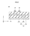
- Fig. 2 is a cross-sectional view illustrating a main part of the wiring substrate 100 of a related art example. It is to be noted that some of the components/elements illustrated in Fig. 2 are omitted in Fig. 1 .
- the cross-sectional view of Fig. 2 is taken along line A-A of Fig. 1 .
- the wiring substrate 100 has a reference layer 170, an insulation layer, and wirings 150, 160 layered thereon.
- the insulation layer 110 includes a glass cloth 120 and a thermosetting resin 130.
- the glass cloth 120 includes glass fiber bundles 120a, 120b.
- the glass fiber bundles 120a, 120b are impregnated in the thermosetting resin 130.
- the glass cloth 120 is formed by plain-weaving the glass fiber bundles 120a, 120b in a grid pattern in which the glass fiber bundles 120a are arranged in parallel with an X axis and spaced apart from each other at substantially constant intervals and the glass fiber bundles 120b are arranged in parallel with a Y axis and spaced apart from each other at substantially constant intervals.
- the holes (i.e. so-called basket holes) 120x created by forming the glass fiber bundles 120a, 120 are filled with the thermosetting resin 130. No glass fiber exists inside the holes 120x.
- the wirings 150, 169 are selectively formed on a part(s) of a surface on one side of the insulation layer 110, and the reference layer 170 are formed substantially on the entire surface on the other side of the insulation layer 110.
- the wirings 150, 160 are conductors having predetermined electric signals flowing therethrough.
- the reference surface 170 is a conductor serving as a return circuit of the predetermined electric signals that flow through the wirings 150, 160.
- the wirings 150, 160 which are arranged alongside each other, are differential wirings used for differential signaling. In general, differential signaling can achieve satisfactory high speed transmission.
- the wiring 150 is positioned on top of the glass fiber bundle 120b.
- the wiring 160 is positioned in-between adjacent glass fiber bundles 120b.
- a wiring substrate of a related art example has glass fiber bundles woven as a grid pattern at a stage where the wiring substrate is a material. Because the wiring substrate of the related art example, in general, has differential wirings arranged in X and Y directions, the differential wirings are arranged in parallel or orthogonal with respect to the direction in which the glass fiber bundles are arranged. This is noticeable particularly for differential wirings used for connecting electronic components (e.g., LSI (Large Scale Integration).
- LSI Large Scale Integration
- differential voltage cannot be initiated due to time lag between the differential wirings at a signal receiving side.
- This time lag tends to be noticeable particularly when transmission distance is long and is a problem for high speed transmission.
- terminals of a typical electronic component are arranged as a rectangle.
- differential wirings diagonally with respect to glass fiber bundles arranged as a grid pattern.
- the glass fibers of the wiring substrate material are to be cut out diagonally in a case where the wiring substrate material is a ready-made belt-like material. This results to waste of the wiring substrate material.
- the glass fibers diagonally there is a problem of requiring new investment in plant and machinery.
- substrate manufacturing conditions is to be reconsidered in a case of fabricating glass fibers diagonally with respect to the outer configuration of the substrate because factors such as shrinkage rate of resin during a substrate laminating process or a perforating process are different compared to a substrate manufacturing method of a related art example.
- a wiring substrate including an insulation layer including a thermosetting resin and a reinforcement member having plural first fiber bundles and plural second fiber bundles woven together, the second fiber bundles being intersected with the first fiber bundles, and a pair of differential wirings arranged alongside each other on the insulation layer, wherein the first fiber bundles and the second fiber bundles have a curved portion relative to a plan direction of the insulation layer in a region on which the pair of differential wirings is arranged.
- Fig. 3 is a plan transparent view illustrating a main part of a wiring substrate 10 according to a first embodiment of the present invention.
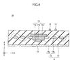
- Fig. 4 is a cross-sectional view illustrating a main part of the wiring substrate 10 according to the first embodiment of the present invention. It is to be noted that some of the components/elements illustrated in Fig. 4 are omitted in Fig. 3 .
- the cross-sectional view of Fig. 4 is taken along line A-A of Fig. 3 .
- the wiring substrate 10 has a reference layer 17, an insulation layer 11, and wirings 15, 16 layered thereon.
- the elements (components) of the wiring substrate 10 are described in detail below.
- the insulation layer 11 includes a glass cloth 12, a thermosetting resin 13, and a fine-size component 14.
- the glass cloth 12 includes glass fiber bundles 12a, 12b.
- the glass fiber bundles 12a, 12b are impregnated in the thermosetting resin 13.
- Each string of fiber of the glass fiber bundles 12a, 12b has a diameter of, for example, a several ⁇ m.
- By bundling the strings of fibers the glass fiber bundles 12a, 12b are formed having a diameter of, for example, several hundred ⁇ m.
- the holes (i.e. so-called basket holes) 12x created by forming the glass fiber bundles 12a, 12b are filled with the thermosetting resin 13. No glass fiber exists inside the holes 12x.
- the material of the thermosetting resin 13 may be, for example, epoxy resin, polyimide resin, or polyester resin.
- the thermosetting resin 13 may contain a filler such as silica or alumina.
- the glass cloth 12 is a reinforcement member formed by weaving (e.g., plain weaving) the glass fiber bundles 12a, 12b in a grid pattern in which the glass fiber bundles 12a are arranged in parallel with an X axis and spaced apart from each other at substantially constant intervals and the glass fiber bundles 12b are arranged in parallel with a Y axis and spaced apart from each other at substantially constant intervals.
- Fine-size components 14 are inserted in some of the holes 12x formed by the adjacently arranged glass fiber bundles 12a and glass fiber bundles 12b.
- the grid pattern of the glass cloth 12 is bent (deformed) at predetermined regions surrounding the parts where the fine-size components 14 are inserted (hereinafter also simply referred to as "predetermined insertion regions").
- predetermined insertion regions the glass fiber bundles 12a are no longer parallel to the X axis but have a curved portion relative to a plan direction (direction parallel to the X-Y plane) of the insulation layer 11.
- the intervals of the glass fiber bundles 12a are inconsistent.
- a pitch between adjacent glass fiber bundles 12a is varied with location in the predetermined regions surrounding the parts where the fine-size components 14 are inserted (i.e. regions on which the wirings 15, 16 are arranged).
- the glass fiber bundles 12a have a curved portion formed in a manner that the intervals become widest near the fine-size components 14 and become narrower the farther from the fine-size components 14 in the X direction.
- the glass fiber bundles 12b are no longer parallel to the Y axis but have a curved portion relative to a plan direction of the insulation layer 11.
- the intervals of the glass fiber bundles 12b are inconsistent. That is, a pitch between adjacent glass fiber bundles 12b is varied with location in the predetermined regions surrounding the parts where the fine-size components 14 are inserted (i.e. regions on which the wirings 15, 16 are arranged).
- the glass fiber bundles 12b have a curved portion formed in a manner that the intervals become widest near the fine-size components 14 and become narrower the farther from the fine-size components 14 in the Y direction.
- the diameter of the fine-size component 14 is set to be greater than the intervals between adjacently arranged glass fiber bundles 12a prior to inserting the fine-size components 14 and the intervals between adjacently arranged glass fiber bundles 12b prior to inserting the fine-size components 14. That is, the holes 12x, which are surrounded by the glass fiber bundles 12a, 12b, are formed having different dimension therebetween in the region on which the wirings 15, 16 are arranged. Accordingly, among the holes 12x, the holes 12x into which the fine-size components 14 are expanded in the plan direction. Thereby, the glass fiber bundles 12a, 12b are bent and form a curved shape.
- the intervals between adjacently arranged glass fiber bundles 12a and the intervals between adjacently arranged glass fiber bundles 12b become wider compared to the state before the fine-size components 14 are inserted.
- the diameter of the fine-size component 14 may be increased so that the diameter of the fine-size component 14 is greater than the intervals of the glass fiber bundles 12a or the intervals of the glass fiber bundles 12b having greater width.
- the intervals between adjacently arranged glass fiber bundles 12a prior to inserting the fine-size components 14 and the intervals between adjacently arranged glass fiber bundles 12b prior to inserting the fine-size components 14 may range from approximately 100 ⁇ m to 500 ⁇ m.
- a bundle of plural fiber strings of carbon fiber, polyester fiber, tetron fiber, nylon fiber, or aramid fiber may be used as alternatives of the glass fiber bundles 12a, 12b formed by bundling together plural fiber strings of glass fiber.
- the method of weaving the glass fiber bundles 12a, 12b is not limited to plain-weaving. For example, satin weaving or twill weaving may be used as the method of weaving the glass fiber bundles 12a, 12b or the other alternatives of the glass fiber bundles 12a, 12b.
- the fine-size component 14 may have any shape as long as the intervals between the adjacently arranged glass fiber bundles 12a, 12b can be widened by inserting the fine-size component 14.
- the fine-size component 14 includes an introduction part 14a having a triangular pyramid-shape, an interval maintaining part 14b having a circular cylinder shape, and a stopper part 14c having circle planar shape with a diameter greater than that of the interval maintaining part 14b.
- the fine-size component 14 may be formed without the introduction part 14a and the stopper part 14c and formed including only the interval maintaining part 14b.
- the diameter of the interval maintaining part 14b of the fine-size component 14 may range, for example, from approximately 200 ⁇ m to 1000 ⁇ m.
- the thickness of the interval maintaining part 14b of the fine-size component 14 may range, for example, from approximately 20 ⁇ m to 200 ⁇ m.
- the material of the fine-size component 14 may be, for example, glass, resin, or metal.
- the wirings 15, 16 are a pair of differential wirings used for differential signaling.
- the wirings 15, 16 are selectively formed on a part of a surface of one side of the insulation layer 11 and arranged alongside each other.
- the reference layer 17 is formed substantially on the entire surface of the other side of the insulation layer 11.
- the wirings 15, 15 are conductors allowing predetermined electric signals to flow therethrough.
- the reference layer 17 is a conductor serving as a return circuit of the predetermined electric signals that flow through the wirings 15, 16.
- Differential signaling is a method of transmitting signals by using POS signals and NEG signals (inverted POS signals). Differential signaling is used particularly for high speed transmission. For example, POS signals are transmitted through the wirings 15 and NEG signals are transmitted through the wirings 16 arranged alongside the wirings 15.
- the wirings 15 and 16 can achieve satisfactory high speed transmission as long as there is no inconsistent characteristic impedance or fluctuation of transmission speed.
- the width of the wirings 15, 16 may range, for example, from 100 ⁇ m to 200 ⁇ m.
- the pitch of the wirings 15, 16 may range, for example, from 250 ⁇ m to 400 ⁇ m.
- the wirings 15, 16 are arranged parallel to the X axis or the Y axis.
- the wirings 15, 16 may include a portion arranged parallel to the X axis and a portion arranged parallel to the Y axis.
- the distance between the wirings 15 and the wirings 16 of the fine-size component 14 to be 0.2 mm or more. This is preferable, particularly, in a case where the fine-size component 14 is formed of metal because aging of the metal may cause the wirings 15, 16 to short-circuit.
- the material of the wirings 15, 16 and the reference layer 17 is not limited in particular as long as the material is a conductor.
- the wirings 15, 16, and the reference layer 17 may be formed of, for example, copper (Cu), aluminum (Al), gold (Au), or silver (Ag).
- the glass fiber bundles 12a are curved along the X direction and are not parallel to the X direction. Further, in the predetermined regions surrounding the parts where the fine-size components 14 are inserted, the glass fiber bundles 12b are curved along the Y direction and are not parallel to the X direction.
- the wirings 15, 16 are arranged parallel to the X axis or the Y axis. That is, by arranging the wirings 15, 16 at the predetermined regions surrounding the parts where the fine-size components 14 are inserted, the wirings 15, 16 are positioned above the glass fiber bundles 12a, 12b arranged diagonally relative to the X axis or the Y axis.
- portions of the wirings 15, 16 positioned above the glass fiber bundles 12a, 12b and portions of the wirings 15, 16 positioned in-between the glass fiber bundles 12a and the glass fiber bundles 12b can be evenly arranged on the wiring substrate 10.
- the wiring substrate 10 can reduce adverse effects due inconsistent glass fiber density (sparse and dense parts of glass fiber).
- the wiring substrate 10 can reduce inconsistent characteristic impedance or difference of transmission delay time.
- the wiring substrate 10 can achieve high speed transmission.
- wirings can position wirings diagonally relative to the X axis or the Y axis by arranging the wirings on a wiring substrate having curved glass fiber bundles.
- wirings can be positioned diagonally with respect to glass fiber bundles more easily compared to the method of the related art example.
- Figs. 3 and 4 illustrate the fine-size component 14 inserted to one of the holes 12x of the glass cloth 12, it is preferable to insert plural fine-size components 14 to the holes 12x because the glass fiber bundles 12a, 12b are to be formed curving on a wide area of the wiring substrate 10 so that the wirings 15, 16 are positioned diagonally relative to the X axis or the Y axis.
- a single fine-size component 14 may be inserted to a hole having a diameter ranging from, for example, approximately 2 mm to 10 mm.
- Fig. 5 is a schematic diagram illustrating plural fine-size components 14 inserted to the glass cloth 12 in a linear manner. As illustrated in Fig.
- the glass fiber bundles 12a, 12b can periodically curve throughout the wiring substrate 10 in a plan direction so that the wirings 15, 16 can be positioned diagonally relative to the X axis or the Y axis.
- Fig. 5 illustrate plural fine-size components 14 inserted to the holes 12x of the glass cloth 12 in a linear manner (grid pattern)
- the plural fine-size components 14 may be inserted to the holes 12x of the glass cloth 12 in a staggered manner (zigzag).
- FIG. 7 is a schematic diagram illustrating processes 21-24 for manufacturing a glass cloth 12 according to an embodiment of the present invention.
- the glass fiber bundles 12 are supplied in the arrow direction A.
- the glass fiber bundles 12b are supplied in the arrow direction B.
- the glass fiber bundles 12a supplied in the first process and the glass fiber bundles 12b supplied in the second process are woven (e.g., plain-woven).
- the glass fiber bundles 12a and the glass fiber bundles 12b may be woven, for example, in a manner intersecting with each other. Thereby, the glass cloth 12 can be fabricated.
- the fine-size components 14 are inserted to predetermined holes 12x of the glass cloth 12.
- the fine-size components 14 are inserted to the corresponding holes 12x having a diameter ranging from, for example, approximately 2 mm to 10 mm.
- the grid pattern of the glass cloth 12 deforms.
- the glass fiber bundles 12a, 12b have curved portions relative to the plan direction.
- the intervals (Y-direction intervals) of the glass fiber bundles 12a adjacent to the fine-size components 14 are not constant. That is, the intervals of the glass fiber bundles 12a become widest the closer towards the fine-size components 14 and become narrower the farther away from the fine-size components 14 in the X-direction.
- the glass fiber bundles 12a are curved along the X-direction. Further, in the predetermined regions surrounding the parts where the fine-size components 14 are inserted, the intervals (X-direction intervals) of the glass fiber bundles 12b adjacent to the fine-size components 14 are not constant. That is, the intervals of the glass fiber bundles 12b become widest the closer towards the fine-size components 14 and become narrower the farther away from the fine-size components 14 in the Y-direction. Thereby, the glass fiber bundles 12b are curved along the Y-direction.
- the holes 12x to which the fine-size components 14 are inserted may be widened with, for example, a needle-like pointed projecting part before the fine-size components 14 are inserted. Then, in a fourth process (roll-up process) 24, the glass cloth 12 inserted with the fine-size components 14 is rolled up.
- Fig. 8 is a schematic diagram illustrating processes 31-37 for manufacturing a wiring substrate 10 according to an embodiment of the present invention.
- the glass cloth 12 fabricated by the processes illustrated in Fig. 7 is used in wiring substrate manufacturing method illustrated in Fig. 8 .
- a first process glass cloth supplying process
- the glass cloth 12 inserted with the fine-size components 14 is supplied.
- the glass cloth inserted with the fine-size components 14 is impregnated in the thermosetting resin 13 (e.g., epoxy resin).
- the thermosetting resin 13 e.g., epoxy resin
- thermosetting resin 13 is dried.
- the insulation stage 13 is in a B-stage state (partially cured state).
- a fourth process (cutting process) 34 the glass cloth 12 impregnated in the thermosetting resin 12 is cut into plural insulation layers 11.
- a fourth process (copper foil adhering process) 35 a copper foil 19 is adhered to both surfaces of each insulation layer 11. It is to be noted that, lastly, one of the copper foils 19 become the wirings 15, 16, and the other one of the copper foils 19 may be the reference layer 17.
- a fifth process (pressing process) 36 the plural insulation layers 11 having the copper foils 19 adhered thereto are subject to a press molding process and a curing process. Thereby, the thermosetting resin 13 is fully cured.
- a sixth process (separating process) 37 the press-molded plural insulation layers 11 are separated. Thereby, plural insulation layers 11 having copper foils 19 formed on both surfaces can be obtained.
- the wirings 15, 16 are formed by performing a known method (e.g., etching) on one of the surfaces of the insulation layer 11. Thereby, the wiring substrate 10 illustrated in Figs. 3 and 4 can be obtained.
- the fine-size components 14 are formed of metal, it is preferable to etch a portion of the copper foil 19 on both surfaces of the insulation layer 11, so that no copper foil 19 exists in the area surrounding the fine-size components 14. Thereby, short-circuiting between the fine-size components 14 and the copper foil 19 can be prevented.
- the wiring substrate 10 may be formed having a multilayer structure by alternately forming an insulation layer(s) and a wiring layer(s) on top of the insulation layer 11 on which the wirings 15, 16 are formed.
- the insulation layer to be formed on top of the insulation layer 11 is preferred to be configured in the same manner as the insulation layer 11 (i.e. configuration having glass fiber bundles of the glass cloth positioned diagonally relative to the X axis or the Y axis). This is for preventing inconsistent characteristic impedance of differential wiring, reducing difference of transmission delay time, and achieving high speed transmission.
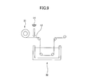
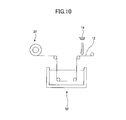
- the fine-size components 14 may be inserted before the resin impregnation process (see Fig. 9 ) or after the resin impregnation process (see Fig. 10 ).
- glass cloth can be bent (deformed) at regions surrounding the parts where fine-size components are inserted.
- glass fiber bundles forming the glass cloth can be positioned diagonally relative to the X axis or the Y axis.
- differential wirings parallel to the X axis or the Y axis on the glass cloth including the diagonally positioned glass fiber bundles, portions of the differential wirings positioned above the glass fiber bundles and portions of the differential wirings positioned in-between the glass fiber bundles (i.e. positioned above the thermosetting resin) can be evenly arranged on the wiring substrate.
- the wiring substrate according to the first embodiment of the present invention can reduce adverse effects due inconsistent glass fiber density (sparse and dense parts of glass fiber). Further, the wiring substrate according to the first embodiment of the present invention can reduce inconsistent characteristic impedance or difference of transmission delay time. Thus, the wiring substrate according to the first embodiment of the present invention can achieve high speed transmission.
- the first embodiment of the present invention does not need to diagonally cut out the glass fiber bundles from a ready-made belt-like material. Thus, wasting of material can be prevented. Because the shrinkage of resin in a substrate laminating process or a perforating process is substantially the same as the related art example, there is no need to reconsider the conditions for manufacturing the wiring substrate. That is, adverse effects due inconsistent glass fiber density (sparse and dense parts of glass fiber) can be easily reduced by the wiring substrate and the method for manufacturing the wiring substrate according to the above-described first embodiment of the present invention.
- a wiring substrate 40 is formed having the fine-size component 14 removed after the glass fiber bundles 12a, 12b are diagonally positioned relative to the X axis or the Y axis by the fine-size component 14 being inserted into the glass cloth 12.
- Fig. 11 is a plan transparent view illustrating a main part of a wiring substrate 40 according to the first modified example of the first embodiment.
- Fig. 12 is a cross-sectional view illustrating a main part of the wiring substrate 40 of the first modified example of the first embodiment. It is to be noted that some of the components/elements illustrated in Fig. 12 are omitted in Fig. 11 .
- the cross-sectional view of Fig. 12 is taken along line C-C of Fig. 11 .
- the wiring substrate 40 is different from the wiring substrate 10 in that the wiring substrate 40 includes no fine-size components 14.
- like components are denoted with like reference numerals and are not described in further detail.
- the wiring substrate 40 is configured having the fine-size component 14 removed after the glass fiber bundles 12a, 12b are diagonally positioned relative to the X axis or the Y axis owing to the bending at predetermined insertion regions of the glass cloth 12 caused by inserting the fine-size component 14 into the glass cloth 12.
- the fine-size component 14 is inserted before the weaving process 23 (see Fig. 7 ) or the resin impregnation process 32 (see Fig. 9 ) and removed after the resin impregnation process (see Fig. 13 ). Because the thermosetting resin 13 is in a B-stage state (partially cured state), the glass cloth 12 remains bent and does not return to its initial shape even after the fine-size component 14 is removed. Then, because the thermosetting resin 13 is fully cured in the pressing process 36, the glass fiber bundles 12a, 12b are maintained in a position diagonal relative to the X axis or the Y axis.
- plural fine-size components 14 may be inserted to the glass cloth 12 to cause the glass cloth 12 to bend and position the glass fiber bundles 12a, 12b to diagonal relative to the X axis or the Y axis as illustrated in Fig. 5 or Fig. 6 . Then, after the insertion of the plural fine-size components 14, the plural fine-size components 14 may be removed from the glass cloth 12.
- the first modified example of the first embodiment can attain the same advantages (effects) as those of the first embodiment because the glass fiber bundles 12a, 12b maintain a diagonal position relative to the X axis or the Y axis even after the fine-size component 14 is removed after inserting the fine-size component and causing the predetermined insertion region of the glass cloth 12 to bend.
- a fine-size component 54 is formed having a shape different from the fine-size component 14 of the first embodiment.
- Fig. 14 is a cross-sectional view illustrating a main part of a wiring substrate 50 of the second modified example of the first embodiment. With reference to Fig. 14 , the wiring substrate 50 is different from the wiring substrate 10 in that the fine-size component 14 is replaced with the fine-size component 54.
- like components are denoted with like reference numerals of the wiring substrate 10 and are not described in further detail.
- the fine-size component 54 having the shape illustrated in Fig. 14 may be used instead of the fine-size component 14.
- the fine-size component 54 has a shape in which a circular cylindrical shaped interval maintaining part 54b is interposed between a circular disk shaped stopper part 54a and a circular disk shaped stopper part 54b by providing the stopper part 54a beneath the interval maintaining part 54b and providing the stopper part 54c on top of the interval maintaining part 54b.
- Each of the stopper parts 54a, 54c has a diameter larger than the diameter of the interval maintaining part 54b.
- the fine-size component 54 may be inserted or pressed into the hole 12x of the glass cloth 12 before the weaving process 23 (see Fig. 7 ), before the resin impregnation process 32 (see Fig. 9 ) or after the resin impregnation process 32 (see Fig. 10 ).
- a fine-size component 51 which includes an introduction part 51a having a triangular pyramid-shape, an interval maintaining part 51 b having a circular cylinder shape, and a stopper part 51cc having circle planar shape with a diameter greater than that of the interval maintaining part 51 b, may be inserted to the hole 12x of the glass cloth 12.
- the shape of the fine-size component 51 may be deformed into the shape of the fine-size component 54 by applying pressure to the top and bottom of the fine-size component 51 as illustrated in Fig. 15B .
- the second modified example of the first embodiment can attain the same advantages (effects) as those of the first embodiment.
- a fine-size component 64 is formed having yet another shape different from the fine-size component 14 of the first embodiment.
- Fig. 16 is a cross-sectional view illustrating a main part of a wiring substrate 60 of the third modified example of the first embodiment. With reference to Fig. 16 , the wiring substrate 60 is different from the wiring substrate 10 in that the fine-size component 14 is replaced with the fine-size component 64.
- like components are denoted with like reference numerals of the wiring substrate 10 and are not described in further detail.
- the fine-size component 64 having a spherical shape may be used instead of the fine-size component 14. Similar as the fine-size component 14, the fine-size component 64 may be inserted or pressed into the hole 12x of the glass cloth 12 before the weaving process 23 (see Fig. 7 ), before the resin impregnation process 12 (see Fig. 9 ), or after the resin impregnation process (see Fig. 10 ).
- a spherical fine-size component 74 which has a diameter less than that of the fine-size component 64, may be inserted to the hole 12x of the glass cloth 12.
- the shape of the fine-size component 74 may be deformed into a circular cylindrical shaped fine-size component 84 by applying pressure to the top and bottom of the fine-size component 74 as illustrated in Fig. 17B .
- the diameter of the fine-size component 84 becomes larger than the diameter of the fine-size component 74.
- the third modified example of the first embodiment can attain the same advantages (effects) as those of the first embodiment.
Landscapes
- Engineering & Computer Science (AREA)
- Textile Engineering (AREA)
- Microelectronics & Electronic Packaging (AREA)
- Chemical & Material Sciences (AREA)
- Inorganic Chemistry (AREA)
- Production Of Multi-Layered Print Wiring Board (AREA)
- Structure Of Printed Boards (AREA)
Abstract
Description
- FIELD The embodiments discussed herein are related to a wiring substrate having a differential wiring formed on an insulation layer and a method for manufacturing the wiring substrate.
-
Fig. 1 is a plan transparent view illustrating a main part of awiring substrate 100 of a related art example.Fig. 2 is a cross-sectional view illustrating a main part of thewiring substrate 100 of a related art example. It is to be noted that some of the components/elements illustrated inFig. 2 are omitted inFig. 1 . The cross-sectional view ofFig. 2 is taken along line A-A ofFig. 1 . - With reference to
Figs. 1 and2 , thewiring substrate 100 has areference layer 170, an insulation layer, andwirings - The
insulation layer 110 includes aglass cloth 120 and athermosetting resin 130. Theglass cloth 120 includesglass fiber bundles glass fiber bundles thermosetting resin 130. Theglass cloth 120 is formed by plain-weaving theglass fiber bundles glass fiber bundles 120a are arranged in parallel with an X axis and spaced apart from each other at substantially constant intervals and theglass fiber bundles 120b are arranged in parallel with a Y axis and spaced apart from each other at substantially constant intervals. The holes (i.e. so-called basket holes) 120x created by forming theglass fiber bundles thermosetting resin 130. No glass fiber exists inside theholes 120x. - The
wirings 150, 169 are selectively formed on a part(s) of a surface on one side of theinsulation layer 110, and thereference layer 170 are formed substantially on the entire surface on the other side of theinsulation layer 110. Thewirings reference surface 170 is a conductor serving as a return circuit of the predetermined electric signals that flow through thewirings - The
wirings wiring 150 is positioned on top of theglass fiber bundle 120b. Thewiring 160 is positioned in-between adjacentglass fiber bundles 120b. - As described above, a wiring substrate of a related art example has glass fiber bundles woven as a grid pattern at a stage where the wiring substrate is a material. Because the wiring substrate of the related art example, in general, has differential wirings arranged in X and Y directions, the differential wirings are arranged in parallel or orthogonal with respect to the direction in which the glass fiber bundles are arranged. This is noticeable particularly for differential wirings used for connecting electronic components (e.g., LSI (Large Scale Integration).
- Because wirings are becoming narrower compared to the pitch of glass fiber bundles, there is a case where one group of the differential wirings are arranged above the glass fiber bundles while another group of the differential wirings are arranged in-between the glass fiber bundles (i.e. above the thermosetting resin) as illustrated in
Figs. 1 and2 . Because dielectric constant of the differential wirings above the glass fiber bundles and dielectric constant of the differential wirings in-between the glass fiber bundles are different due to difference of glass fiber density (areas where glass fiber is dense and area where glass fiber is sparse), the signal transmission rate of the differential wirings above the glass fiber bundles is slower than that of the differential wirings in-between the glass fiber bundles. Therefore, in a case where one group of differential wirings is arranged above the glass fiber bundles while the other group of differential wirings is arranged in-between the glass fiber bundles (i.e. above the thermosetting resin), problems such as inconsistency of characteristic impedance and difference of transmission delay time occur. - In other words, in a case of transmitting voltage where one group of differential wirings are arranged above the glass fiber bundles while the other group of differential wirings are arranged in-between the glass fiber bundles (i.e. above the thermosetting resin), differential voltage cannot be initiated due to time lag between the differential wirings at a signal receiving side. This time lag tends to be noticeable particularly when transmission distance is long and is a problem for high speed transmission. As a countermeasure to this problem, there is, for example, a method of reducing the influence of inconsistent glass fiber density (dense/sparse areas of glass fiber) by arranging the differential wirings diagonally with respect to the glass fiber bundles arranged as a grid pattern.
- However, terminals of a typical electronic component are arranged as a rectangle. Thus, it is difficult to arrange differential wirings diagonally with respect to glass fiber bundles arranged as a grid pattern. Further, although it is possible to weave glass fibers of a wiring substrate material diagonally, the glass fibers of the wiring substrate material are to be cut out diagonally in a case where the wiring substrate material is a ready-made belt-like material. This results to waste of the wiring substrate material. Further, in the case of weaving the glass fibers diagonally, there is a problem of requiring new investment in plant and machinery. In any event, substrate manufacturing conditions is to be reconsidered in a case of fabricating glass fibers diagonally with respect to the outer configuration of the substrate because factors such as shrinkage rate of resin during a substrate laminating process or a perforating process are different compared to a substrate manufacturing method of a related art example.
- According to an aspect of the invention, there is provided a wiring substrate including an insulation layer including a thermosetting resin and a reinforcement member having plural first fiber bundles and plural second fiber bundles woven together, the second fiber bundles being intersected with the first fiber bundles, and a pair of differential wirings arranged alongside each other on the insulation layer, wherein the first fiber bundles and the second fiber bundles have a curved portion relative to a plan direction of the insulation layer in a region on which the pair of differential wirings is arranged.
- The object and advantages of the invention will be realized and attained by means of the elements and combinations particularly pointed out in the claims.
- It is to be understood that both the foregoing generation description and the followed detailed description are exemplary and explanatory and are not restrictive of the invention, as claimed.
-
-
Fig. 1 is a plan transparent view illustrating a main part of a wiring substrate of a related art example; -
Fig. 2 is a cross-sectional view illustrating a main part of a wiring substrate of a related art example; -
Fig. 3 is a plan transparent view illustrating a main part of a wiring substrate according to a first embodiment of the present invention; -
Fig. 4 is a cross-sectional view illustrating a main part of a wiring substrate according to a first embodiment of the present invention; -
Fig. 5 is a schematic diagram illustrating plural fine-size components inserted to a glass cloth in a linear manner according to an embodiment of the present invention; -
Fig. 6 is a schematic diagram illustrating plural fine-size components inserted to a glass cloth in a staggered manner according to an embodiment of the present invention; -
Fig. 7 is a schematic diagram illustrating processes for manufacturing a glass cloth according to an embodiment of the present invention; -
Fig. 8 is a schematic diagram illustrating processes for manufacturing a wiring substrate according to an embodiment of the present invention; -
Fig. 9 is a schematic diagram for illustrating a process of inserting a fine-size component according to an embodiment of the present invention (Part 1); -
Fig. 10 is a schematic diagram for illustrating a process of inserting a fine-size component according to an embodiment of the present invention (Part 2); -
Fig. 11 is a plan transparent view illustrating a main part of a wiring substrate according to a first modified example of the first embodiment; -
Fig. 12 is a cross-sectional view illustrating a main part of the wiring substrate of a first modified example of the first embodiment; -
Fig. 13 is a schematic diagram for illustrating a process of removing a fine-size component according to an embodiment of the present invention; -
Fig. 14 is a cross-sectional view illustrating a main part of a wiring substrate of a second modified example of the first embodiment; -
Figs. 15A and 15B are schematic diagrams for illustrating a process of inserting a fine-size component according to an embodiment of the present invention (Part 1); -
Fig. 16 is a cross-sectional view illustrating a main part of a wiring substrate of a third modified example of the first embodiment; and -
Figs. 17A and 17B are schematic diagrams for illustrating a process of inserting a fine-size component according to an embodiment of the present invention (Part 2). - Embodiments according to the present invention are described with reference to the accompanying drawings.
- With the wiring substrate and method for manufacturing the wiring substrate according to the below-described embodiments of the present invention, effects (advantages) such as easily preventing wirings from being adversely affected by inconsistent glass fiber density (sparse and dense parts of glass fiber).
-
Fig. 3 is a plan transparent view illustrating a main part of awiring substrate 10 according to a first embodiment of the present invention.Fig. 4 is a cross-sectional view illustrating a main part of thewiring substrate 10 according to the first embodiment of the present invention. It is to be noted that some of the components/elements illustrated inFig. 4 are omitted inFig. 3 . The cross-sectional view ofFig. 4 is taken along line A-A ofFig. 3 . - With reference to
Figs. 3 and4 , thewiring substrate 10 has areference layer 17, aninsulation layer 11, and wirings 15, 16 layered thereon. The elements (components) of thewiring substrate 10 are described in detail below. - The
insulation layer 11 includes aglass cloth 12, athermosetting resin 13, and a fine-size component 14. Theglass cloth 12 includesglass fiber bundles glass fiber bundles thermosetting resin 13. Each string of fiber of theglass fiber bundles glass fiber bundles glass fiber bundles thermosetting resin 13. No glass fiber exists inside theholes 12x. The material of thethermosetting resin 13 may be, for example, epoxy resin, polyimide resin, or polyester resin. Thethermosetting resin 13 may contain a filler such as silica or alumina. - The
glass cloth 12 is a reinforcement member formed by weaving (e.g., plain weaving) theglass fiber bundles glass fiber bundles 12a are arranged in parallel with an X axis and spaced apart from each other at substantially constant intervals and theglass fiber bundles 12b are arranged in parallel with a Y axis and spaced apart from each other at substantially constant intervals. Fine-size components 14 are inserted in some of theholes 12x formed by the adjacently arrangedglass fiber bundles 12a andglass fiber bundles 12b. - Thereby, the grid pattern of the
glass cloth 12 is bent (deformed) at predetermined regions surrounding the parts where the fine-size components 14 are inserted (hereinafter also simply referred to as "predetermined insertion regions"). Thus, theglass fiber bundles 12a are no longer parallel to the X axis but have a curved portion relative to a plan direction (direction parallel to the X-Y plane) of theinsulation layer 11. In other words, at the predetermined regions surrounding the parts where the fine-size components 14 are inserted, the intervals of theglass fiber bundles 12a (intervals in the Y direction) adjacent to the fine-size components 14 are inconsistent. That is, a pitch between adjacentglass fiber bundles 12a is varied with location in the predetermined regions surrounding the parts where the fine-size components 14 are inserted (i.e. regions on which thewirings glass fiber bundles 12a have a curved portion formed in a manner that the intervals become widest near the fine-size components 14 and become narrower the farther from the fine-size components 14 in the X direction. - Likewise, because the grid pattern of the
glass cloth 12 is bent at predetermined regions surrounding the parts where the fine-size components 14 are inserted, theglass fiber bundles 12b are no longer parallel to the Y axis but have a curved portion relative to a plan direction of theinsulation layer 11. In other words, at the predetermined regions surrounding the parts where the fine-size components 14 are inserted, the intervals of theglass fiber bundles 12b (intervals in the X direction) adjacent to the fine-size components 14 are inconsistent. That is, a pitch between adjacentglass fiber bundles 12b is varied with location in the predetermined regions surrounding the parts where the fine-size components 14 are inserted (i.e. regions on which thewirings glass fiber bundles 12b have a curved portion formed in a manner that the intervals become widest near the fine-size components 14 and become narrower the farther from the fine-size components 14 in the Y direction. - The diameter of the fine-
size component 14 is set to be greater than the intervals between adjacently arrangedglass fiber bundles 12a prior to inserting the fine-size components 14 and the intervals between adjacently arrangedglass fiber bundles 12b prior to inserting the fine-size components 14. That is, theholes 12x, which are surrounded by theglass fiber bundles wirings holes 12x, theholes 12x into which the fine-size components 14 are expanded in the plan direction. Thereby, theglass fiber bundles glass fiber bundles 12a and the intervals between adjacently arrangedglass fiber bundles 12b become wider compared to the state before the fine-size components 14 are inserted. In a case where the width of the intervals between adjacently arrangedglass fiber bundles 12a prior to inserting the fine-size components 14 is different from the width of the intervals between adjacently arrangedglass fiber bundles 12b prior to inserting the fine-size components 14, the diameter of the fine-size component 14 may be increased so that the diameter of the fine-size component 14 is greater than the intervals of theglass fiber bundles 12a or the intervals of theglass fiber bundles 12b having greater width. - For example, the intervals between adjacently arranged
glass fiber bundles 12a prior to inserting the fine-size components 14 and the intervals between adjacently arrangedglass fiber bundles 12b prior to inserting the fine-size components 14 may range from approximately 100 µm to 500 µm. - A bundle of plural fiber strings of carbon fiber, polyester fiber, tetron fiber, nylon fiber, or aramid fiber may be used as alternatives of the
glass fiber bundles glass fiber bundles glass fiber bundles glass fiber bundles glass fiber bundles - The fine-
size component 14 may have any shape as long as the intervals between the adjacently arrangedglass fiber bundles size component 14. In the example illustrated inFigs. 3 and4 , the fine-size component 14 includes anintroduction part 14a having a triangular pyramid-shape, aninterval maintaining part 14b having a circular cylinder shape, and astopper part 14c having circle planar shape with a diameter greater than that of theinterval maintaining part 14b. In an alternative example, the fine-size component 14 may be formed without theintroduction part 14a and thestopper part 14c and formed including only theinterval maintaining part 14b. The diameter of theinterval maintaining part 14b of the fine-size component 14 may range, for example, from approximately 200 µm to 1000 µm. The thickness of theinterval maintaining part 14b of the fine-size component 14 may range, for example, from approximately 20 µm to 200 µm. The material of the fine-size component 14 may be, for example, glass, resin, or metal. - The
wirings wirings insulation layer 11 and arranged alongside each other. Thereference layer 17 is formed substantially on the entire surface of the other side of theinsulation layer 11. Thewirings reference layer 17 is a conductor serving as a return circuit of the predetermined electric signals that flow through thewirings wirings 15 and NEG signals are transmitted through thewirings 16 arranged alongside thewirings 15. Thewirings - The width of the
wirings wirings wirings wirings wirings 15 and thewirings 16 of the fine-size component 14 to be 0.2 mm or more. This is preferable, particularly, in a case where the fine-size component 14 is formed of metal because aging of the metal may cause thewirings wirings reference layer 17 is not limited in particular as long as the material is a conductor. However, thewirings reference layer 17 may be formed of, for example, copper (Cu), aluminum (Al), gold (Au), or silver (Ag). - In the predetermined regions surrounding the parts where the fine-
size components 14 are inserted, theglass fiber bundles 12a are curved along the X direction and are not parallel to the X direction. Further, in the predetermined regions surrounding the parts where the fine-size components 14 are inserted, theglass fiber bundles 12b are curved along the Y direction and are not parallel to the X direction. On the other hand, thewirings wirings size components 14 are inserted, thewirings glass fiber bundles - Accordingly, portions of the
wirings glass fiber bundles wirings glass fiber bundles 12a and theglass fiber bundles 12b (i.e. positioned above the thermosetting resin) can be evenly arranged on thewiring substrate 10. As a result, compared to the wiring substrate of the related art example, thewiring substrate 10 can reduce adverse effects due inconsistent glass fiber density (sparse and dense parts of glass fiber). Further, thewiring substrate 10 can reduce inconsistent characteristic impedance or difference of transmission delay time. Thus, thewiring substrate 10 can achieve high speed transmission. - According to the above-described related art example, there is a method of arranging wirings diagonally relative to the X axis or the Y axis on a glass cloth having glass fiber bundles arranged parallel to the X axis or the Y axis. Unlike the method of the relative art example, the above-described embodiment of the present invention wirings can position wirings diagonally relative to the X axis or the Y axis by arranging the wirings on a wiring substrate having curved glass fiber bundles. Thus, wirings can be positioned diagonally with respect to glass fiber bundles more easily compared to the method of the related art example.
- Although
Figs. 3 and4 illustrate the fine-size component 14 inserted to one of theholes 12x of theglass cloth 12, it is preferable to insert plural fine-size components 14 to theholes 12x because theglass fiber bundles wiring substrate 10 so that thewirings size component 14 may be inserted to a hole having a diameter ranging from, for example, approximately 2 mm to 10 mm.Fig. 5 is a schematic diagram illustrating plural fine-size components 14 inserted to theglass cloth 12 in a linear manner. As illustrated inFig. 5 , by inserting the fine-size component 14 to thehole 12x of theglass cloth 12 having a diameter ranging from, for example, approximately 2 mm to 10 mm, theglass fiber bundles wiring substrate 10 in a plan direction so that thewirings - It is to be noted that, although
Fig. 5 illustrate plural fine-size components 14 inserted to theholes 12x of theglass cloth 12 in a linear manner (grid pattern), the plural fine-size components 14 may be inserted to theholes 12x of theglass cloth 12 in a staggered manner (zigzag). - Next, a method for manufacturing a wiring substrate according to the first embodiment of the present invention is described.
Fig. 7 is a schematic diagram illustrating processes 21-24 for manufacturing aglass cloth 12 according to an embodiment of the present invention. With reference toFig. 7 , in afirst process 21 for manufacturing theglass cloth 12, theglass fiber bundles 12 are supplied in the arrow direction A. Then, in asecond process 22 for manufacturing theglass cloth 12, theglass fiber bundles 12b are supplied in the arrow direction B. - Then, in a third process (weaving process) 23 for manufacturing the
glass cloth 12, theglass fiber bundles 12a supplied in the first process and theglass fiber bundles 12b supplied in the second process are woven (e.g., plain-woven). Theglass fiber bundles 12a and theglass fiber bundles 12b may be woven, for example, in a manner intersecting with each other. Thereby, theglass cloth 12 can be fabricated. In the third process, the fine-size components 14 are inserted topredetermined holes 12x of theglass cloth 12. The fine-size components 14 are inserted to the correspondingholes 12x having a diameter ranging from, for example, approximately 2 mm to 10 mm. - Accordingly, the
holes 12x to which the fine-size components 14 are enlarged in the plan direction compared toother holes 12x. Thereby, the grid pattern of theglass cloth 12 deforms. As a result, theglass fiber bundles size components 14 are inserted, the intervals (Y-direction intervals) of theglass fiber bundles 12a adjacent to the fine-size components 14 are not constant. That is, the intervals of theglass fiber bundles 12a become widest the closer towards the fine-size components 14 and become narrower the farther away from the fine-size components 14 in the X-direction. Thereby, theglass fiber bundles 12a are curved along the X-direction. Further, in the predetermined regions surrounding the parts where the fine-size components 14 are inserted, the intervals (X-direction intervals) of theglass fiber bundles 12b adjacent to the fine-size components 14 are not constant. That is, the intervals of theglass fiber bundles 12b become widest the closer towards the fine-size components 14 and become narrower the farther away from the fine-size components 14 in the Y-direction. Thereby, theglass fiber bundles 12b are curved along the Y-direction. - The
holes 12x to which the fine-size components 14 are inserted may be widened with, for example, a needle-like pointed projecting part before the fine-size components 14 are inserted. Then, in a fourth process (roll-up process) 24, theglass cloth 12 inserted with the fine-size components 14 is rolled up. -
Fig. 8 is a schematic diagram illustrating processes 31-37 for manufacturing awiring substrate 10 according to an embodiment of the present invention. Theglass cloth 12 fabricated by the processes illustrated inFig. 7 is used in wiring substrate manufacturing method illustrated inFig. 8 . With reference toFig. 8 , in a first process (glass cloth supplying process) 31, theglass cloth 12 inserted with the fine-size components 14 is supplied. Then, in a second process (resin impregnation process) 32, the glass cloth inserted with the fine-size components 14 is impregnated in the thermosetting resin 13 (e.g., epoxy resin). - Then, in a third process (drying process) 33, the
thermosetting resin 13 is dried. In the drying process, theinsulation stage 13 is in a B-stage state (partially cured state). Then, in a fourth process (cutting process) 34, theglass cloth 12 impregnated in thethermosetting resin 12 is cut into plural insulation layers 11. Then, in a fourth process (copper foil adhering process) 35, acopper foil 19 is adhered to both surfaces of eachinsulation layer 11. It is to be noted that, lastly, one of the copper foils 19 become thewirings reference layer 17. - Then, in a fifth process (pressing process) 36, the plural insulation layers 11 having the copper foils 19 adhered thereto are subject to a press molding process and a curing process. Thereby, the
thermosetting resin 13 is fully cured. Then, in a sixth process (separating process) 37, the press-molded plural insulation layers 11 are separated. Thereby, plural insulation layers 11 having copper foils 19 formed on both surfaces can be obtained. After theseparating process 37, thewirings insulation layer 11. Thereby, thewiring substrate 10 illustrated inFigs. 3 and4 can be obtained. It is to be noted that, in a case where the fine-size components 14 are formed of metal, it is preferable to etch a portion of thecopper foil 19 on both surfaces of theinsulation layer 11, so that nocopper foil 19 exists in the area surrounding the fine-size components 14. Thereby, short-circuiting between the fine-size components 14 and thecopper foil 19 can be prevented. - Further, the
wiring substrate 10 may be formed having a multilayer structure by alternately forming an insulation layer(s) and a wiring layer(s) on top of theinsulation layer 11 on which thewirings insulation layer 11 is preferred to be configured in the same manner as the insulation layer 11 (i.e. configuration having glass fiber bundles of the glass cloth positioned diagonally relative to the X axis or the Y axis). This is for preventing inconsistent characteristic impedance of differential wiring, reducing difference of transmission delay time, and achieving high speed transmission. - Instead of inserting the fine-
size components 14 to correspondingholes 12x of theglass cloth 12 in theweaving process 23 ofFig. 7 , the fine-size components 14 may be inserted before the resin impregnation process (seeFig. 9 ) or after the resin impregnation process (seeFig. 10 ). - With the configuration of the wiring substrate and the method for manufacturing the wiring substrate according to the above-described first embodiment of the present invention, glass cloth can be bent (deformed) at regions surrounding the parts where fine-size components are inserted. Thereby, glass fiber bundles forming the glass cloth can be positioned diagonally relative to the X axis or the Y axis. By arranging differential wirings parallel to the X axis or the Y axis on the glass cloth including the diagonally positioned glass fiber bundles, portions of the differential wirings positioned above the glass fiber bundles and portions of the differential wirings positioned in-between the glass fiber bundles (i.e. positioned above the thermosetting resin) can be evenly arranged on the wiring substrate. As a result, compared to a wiring substrate of a related art example, the wiring substrate according to the first embodiment of the present invention can reduce adverse effects due inconsistent glass fiber density (sparse and dense parts of glass fiber). Further, the wiring substrate according to the first embodiment of the present invention can reduce inconsistent characteristic impedance or difference of transmission delay time. Thus, the wiring substrate according to the first embodiment of the present invention can achieve high speed transmission.
- With the above-described first embodiment of the present invention, there is no need to arrange wirings diagonally with respect to glass fiber bundles woven in a grid pattern. Therefore, the wirings can be easily fabricated. Unlike a method of forming glass fiber bundles of a wiring substrate material diagonally according to a related art example, the first embodiment of the present invention does not need to diagonally cut out the glass fiber bundles from a ready-made belt-like material. Thus, wasting of material can be prevented. Because the shrinkage of resin in a substrate laminating process or a perforating process is substantially the same as the related art example, there is no need to reconsider the conditions for manufacturing the wiring substrate. That is, adverse effects due inconsistent glass fiber density (sparse and dense parts of glass fiber) can be easily reduced by the wiring substrate and the method for manufacturing the wiring substrate according to the above-described first embodiment of the present invention.
- In the first modified example of the first embodiment, a
wiring substrate 40 is formed having the fine-size component 14 removed after theglass fiber bundles size component 14 being inserted into theglass cloth 12. -
Fig. 11 is a plan transparent view illustrating a main part of awiring substrate 40 according to the first modified example of the first embodiment.Fig. 12 is a cross-sectional view illustrating a main part of thewiring substrate 40 of the first modified example of the first embodiment. It is to be noted that some of the components/elements illustrated inFig. 12 are omitted inFig. 11 . The cross-sectional view ofFig. 12 is taken along line C-C ofFig. 11 . With reference toFigs. 11 and12 , thewiring substrate 40 is different from thewiring substrate 10 in that thewiring substrate 40 includes no fine-size components 14. In thewiring substrate 40, like components are denoted with like reference numerals and are not described in further detail. - The
wiring substrate 40 is configured having the fine-size component 14 removed after theglass fiber bundles glass cloth 12 caused by inserting the fine-size component 14 into theglass cloth 12. The fine-size component 14 is inserted before the weaving process 23 (seeFig. 7 ) or the resin impregnation process 32 (seeFig. 9 ) and removed after the resin impregnation process (seeFig. 13 ). Because thethermosetting resin 13 is in a B-stage state (partially cured state), theglass cloth 12 remains bent and does not return to its initial shape even after the fine-size component 14 is removed. Then, because thethermosetting resin 13 is fully cured in thepressing process 36, theglass fiber bundles - In an alternative example, plural fine-
size components 14 may be inserted to theglass cloth 12 to cause theglass cloth 12 to bend and position theglass fiber bundles Fig. 5 orFig. 6 . Then, after the insertion of the plural fine-size components 14, the plural fine-size components 14 may be removed from theglass cloth 12. - As described above, the first modified example of the first embodiment can attain the same advantages (effects) as those of the first embodiment because the
glass fiber bundles size component 14 is removed after inserting the fine-size component and causing the predetermined insertion region of theglass cloth 12 to bend. - In the second modified example of the first embodiment, a fine-
size component 54 is formed having a shape different from the fine-size component 14 of the first embodiment.Fig. 14 is a cross-sectional view illustrating a main part of awiring substrate 50 of the second modified example of the first embodiment. With reference toFig. 14 , thewiring substrate 50 is different from thewiring substrate 10 in that the fine-size component 14 is replaced with the fine-size component 54. In thewiring substrate 50, like components are denoted with like reference numerals of thewiring substrate 10 and are not described in further detail. - As illustrated in
Fig. 14 , the fine-size component 54 having the shape illustrated inFig. 14 may be used instead of the fine-size component 14. The fine-size component 54 has a shape in which a circular cylindrical shapedinterval maintaining part 54b is interposed between a circular disk shapedstopper part 54a and a circular disk shapedstopper part 54b by providing thestopper part 54a beneath theinterval maintaining part 54b and providing thestopper part 54c on top of theinterval maintaining part 54b. Each of thestopper parts interval maintaining part 54b. The fine-size component 54 may be inserted or pressed into thehole 12x of theglass cloth 12 before the weaving process 23 (seeFig. 7 ), before the resin impregnation process 32 (seeFig. 9 ) or after the resin impregnation process 32 (seeFig. 10 ). - Further, as illustrated in
Fig. 15A , a fine-size component 51, which includes anintroduction part 51a having a triangular pyramid-shape, aninterval maintaining part 51 b having a circular cylinder shape, and a stopper part 51cc having circle planar shape with a diameter greater than that of theinterval maintaining part 51 b, may be inserted to thehole 12x of theglass cloth 12. After inserting the fine-size component 51, the shape of the fine-size component 51 may be deformed into the shape of the fine-size component 54 by applying pressure to the top and bottom of the fine-size component 51 as illustrated inFig. 15B . - Even in a case where the fine-
size component 54 is used instead of the fine-size component 14, the second modified example of the first embodiment can attain the same advantages (effects) as those of the first embodiment. - In the third modified example of the first embodiment, a fine-
size component 64 is formed having yet another shape different from the fine-size component 14 of the first embodiment.Fig. 16 is a cross-sectional view illustrating a main part of awiring substrate 60 of the third modified example of the first embodiment. With reference toFig. 16 , thewiring substrate 60 is different from thewiring substrate 10 in that the fine-size component 14 is replaced with the fine-size component 64. In thewiring substrate 60, like components are denoted with like reference numerals of thewiring substrate 10 and are not described in further detail. - As illustrated in
Fig. 16 , the fine-size component 64 having a spherical shape may be used instead of the fine-size component 14. Similar as the fine-size component 14, the fine-size component 64 may be inserted or pressed into thehole 12x of theglass cloth 12 before the weaving process 23 (seeFig. 7 ), before the resin impregnation process 12 (seeFig. 9 ), or after the resin impregnation process (seeFig. 10 ). - Further, as illustrated in
Fig. 17A , a spherical fine-size component 74, which has a diameter less than that of the fine-size component 64, may be inserted to thehole 12x of theglass cloth 12. After inserting the fine-size component 74, the shape of the fine-size component 74 may be deformed into a circular cylindrical shaped fine-size component 84 by applying pressure to the top and bottom of the fine-size component 74 as illustrated inFig. 17B . By applying pressure to the fine-size component 74, the diameter of the fine-size component 84 becomes larger than the diameter of the fine-size component 74. - Even in a case where the fine-
size component 64 or the fine-size component 84 is used instead of the fine-size component 14, the third modified example of the first embodiment can attain the same advantages (effects) as those of the first embodiment. - All examples and conditional language recited herein are intended for pedagogical purposes to aid the reader in understanding the invention and the concepts contributed by the inventor to furthering the art, and are to be construed as being without limitation to such specifically recited examples and conditions, nor does the organization of such examples in the specification relate to a showing of the superiority and inferiority of the invention. Although the embodiments of the present invention have been described in detail, it should be understood that the various changes, substitutions, and alterations could be made hereto without departing from the spirit and scope of the invention.
Claims (13)
- A wiring substrate comprising:an insulation layer including a thermosetting resin and a reinforcement member having a plurality of first fiber bundles and a plurality of second fiber bundles woven together, the second fiber bundles being intersected with the first fiber bundles; anda pair of differential wirings arranged alongside each other on the insulation layer, the wiring substrate being characterized in thatthe first fiber bundles and the second fiber bundles have a curved portion relative to a plan direction of the insulation layer in a region on which the pair of differential wirings is arranged.
- The wiring substrate as claimed in claim 1, characterized in that a pitch between adjacent first fiber bundles and between adjacent second fiber bundles is varied with location in the region.
- The wiring substrate as claimed in claim 1, characterized by further comprising a plurality of holes surrounded by the first fiber bundles and the second fiber bundles,
wherein the plurality of holes has different dimension therebetween in the region. - The wiring substrate as claimed in claim 3, further comprising a component inserted at least in one of the plurality of holes.
- The wiring substrate as claimed in claim 3, characterized in that the plurality of holes includes a plurality of expanded holes.
- The wiring substrate as claimed in claim 5, characterized in that the expanded holes are arranged in grid pattern or staggered pattern.
- A method for manufacturing a wiring substrate, comprising:forming an insulation layer including an insulating resin and a reinforcement member having a plurality of first fiber bundles and a plurality of second fiber bundles woven together, the second fiber bundles being intersected with the first fiber bundles; and arranging a pair of differential wirings on the insulation layer, the method being characterized by
forming a curved portion on woven first fiber bundles and second fiber bundles relative to a plan direction of the insulation layer in a region on which the pair of differential wirings is arranged. - The method as claimed in claim 7, characterized in that said forming the curved portion comprises varying a pitch between adjacent first fiber bundles and between adjacent second fiber bundles with location in the region.
- The method as claimed in claim 7 or 8, characterized in that said forming the curved portion comprises forming a plurality of holes having different dimension therebetween, the holes being surrounded by the first fiber bundles and the second fiber bundles.
- The method as claimed in claim 9, characterized in that said forming the curved portion comprises inserting a component to at least one of the plurality of holes.
- The method as claimed in claim 10,
characterized by further comprising:removing the component from the holes before said arranging the pair of differential wirings. - The method as claimed in claim 10, characterized in that
said forming the insulation layer comprises impregnating the thermosetting resin with the reinforcement member,
wherein the component is inserted to one of the holes before said impregnating. - The method as claimed in claim 10, characterized in that
said forming the insulation layer comprises impregnating the thermosetting resin with the reinforcement member,
wherein the component is inserted to the holes after said impregnating.
Applications Claiming Priority (1)
| Application Number | Priority Date | Filing Date | Title |
|---|---|---|---|
| JP2010140951A JP5589595B2 (en) | 2010-06-21 | 2010-06-21 | Wiring board and manufacturing method thereof |
Publications (2)
| Publication Number | Publication Date |
|---|---|
| EP2397587A1 true EP2397587A1 (en) | 2011-12-21 |
| EP2397587B1 EP2397587B1 (en) | 2012-12-12 |
Family
ID=44146952
Family Applications (1)
| Application Number | Title | Priority Date | Filing Date |
|---|---|---|---|
| EP11160536A Not-in-force EP2397587B1 (en) | 2010-06-21 | 2011-03-30 | Wiring substrate and method for manufacturing the wiring substrate |
Country Status (3)
| Country | Link |
|---|---|
| US (1) | US9049794B2 (en) |
| EP (1) | EP2397587B1 (en) |
| JP (1) | JP5589595B2 (en) |
Families Citing this family (3)
| Publication number | Priority date | Publication date | Assignee | Title |
|---|---|---|---|---|
| CN105704931B (en) * | 2014-11-28 | 2021-01-22 | 中兴通讯股份有限公司 | Wiring method of differential signal line and PCB |
| WO2016117320A1 (en) * | 2015-01-21 | 2016-07-28 | 日本電気株式会社 | Wiring board and method for designing same |
| JP2019158542A (en) * | 2018-03-13 | 2019-09-19 | 古河電気工業株式会社 | Radar device |
Citations (3)
| Publication number | Priority date | Publication date | Assignee | Title |
|---|---|---|---|---|
| US20040181764A1 (en) * | 2003-03-11 | 2004-09-16 | Brist Gary A. | Conductor trace design to reduce common mode cross-talk and timing skew |
| US20070110388A1 (en) * | 2005-11-17 | 2007-05-17 | Intel Corporation | Method of making a fiber reinforced printed circuit board panel and a fiber reinforced panel made according to the method |
| WO2007109483A1 (en) * | 2006-03-21 | 2007-09-27 | Intel Corporation | Shifted segment layout for differential signal traces to mitigate bundle weave effect |
Family Cites Families (12)
| Publication number | Priority date | Publication date | Assignee | Title |
|---|---|---|---|---|
| US2874209A (en) * | 1953-01-21 | 1959-02-17 | Philips Corp | Support or stay member for parts of the electrode systems of electric discharge tubes |
| JPH065593A (en) * | 1992-04-20 | 1994-01-14 | Sumitomo Electric Ind Ltd | Manufacture of multilayer interconnection substrate |
| JPH0976385A (en) * | 1995-09-11 | 1997-03-25 | Unisia Jecs Corp | Method for producing fiber-reinforced composite material having connecting holes |
| US6727197B1 (en) * | 1999-11-18 | 2004-04-27 | Foster-Miller, Inc. | Wearable transmission device |
| US6447886B1 (en) * | 2000-03-20 | 2002-09-10 | 3Tex, Inc. | Base material for a printed circuit board formed from a three-dimensional woven fiber structure |
| EP1408726B1 (en) * | 2001-07-18 | 2010-02-10 | Panasonic Corporation | Method of manufacturing a printed wiring board |
| US7459200B2 (en) * | 2003-08-15 | 2008-12-02 | Intel Corporation | Circuit board design |
| JP2006100699A (en) | 2004-09-30 | 2006-04-13 | Toshiba Corp | Printed wiring board, information processing apparatus, and printed wiring board manufacturing method |
| US7292454B2 (en) * | 2004-12-03 | 2007-11-06 | Dell Products L.P. | System and method for optimizing printed circuit boards to minimize effects of non-uniform dielectric |
| US20070178289A1 (en) * | 2006-01-27 | 2007-08-02 | International Business Machines Corporation | High-speed routing composite material |
| JP2008171834A (en) * | 2007-01-05 | 2008-07-24 | Hitachi Ltd | Glass cloth wiring board |
| JP2009073946A (en) * | 2007-09-21 | 2009-04-09 | Hitachi Ltd | Insulating substrate, wiring board and multilayer board |
-
2010
- 2010-06-21 JP JP2010140951A patent/JP5589595B2/en not_active Expired - Fee Related
-
2011
- 2011-03-30 EP EP11160536A patent/EP2397587B1/en not_active Not-in-force
- 2011-03-30 US US13/075,865 patent/US9049794B2/en not_active Expired - Fee Related
Patent Citations (3)
| Publication number | Priority date | Publication date | Assignee | Title |
|---|---|---|---|---|
| US20040181764A1 (en) * | 2003-03-11 | 2004-09-16 | Brist Gary A. | Conductor trace design to reduce common mode cross-talk and timing skew |
| US20070110388A1 (en) * | 2005-11-17 | 2007-05-17 | Intel Corporation | Method of making a fiber reinforced printed circuit board panel and a fiber reinforced panel made according to the method |
| WO2007109483A1 (en) * | 2006-03-21 | 2007-09-27 | Intel Corporation | Shifted segment layout for differential signal traces to mitigate bundle weave effect |
Also Published As
| Publication number | Publication date |
|---|---|
| EP2397587B1 (en) | 2012-12-12 |
| US20110308842A1 (en) | 2011-12-22 |
| JP2012004507A (en) | 2012-01-05 |
| US9049794B2 (en) | 2015-06-02 |
| JP5589595B2 (en) | 2014-09-17 |
Similar Documents
| Publication | Publication Date | Title |
|---|---|---|
| KR101751232B1 (en) | Multilayer electronic structure with integral construction elements | |
| JP5097827B2 (en) | Flex-rigid wiring board and electronic device | |
| CN102149251B (en) | Flex-rigid wiring board and method for manufacturing the same | |
| KR20100096274A (en) | Wiring board and method for manufacturing the same | |
| CN101902875B (en) | Multi-layer wire substrate | |
| US9653636B2 (en) | Device for interconnecting photovoltaic cells having contacts on their back side, and module comprising such a device | |
| US20090139751A1 (en) | Wiring substrate and manufacturing method thereof | |
| US8161636B2 (en) | Circuit board and method of manufacturing the same | |
| DE102007048007A1 (en) | Warpage preventing circuit substrate for semiconductor package, has warpage preventing region comprising warpage pattern formed in adjacent corners of substrate and warpage elements provided in diagonal direction of corners | |
| CN104684258A (en) | Strip level substrate including warpage preventing member and method of manufacturing the same | |
| JP6031943B2 (en) | Circuit board, circuit board manufacturing method, electronic device, and glass cloth | |
| EP2397587B1 (en) | Wiring substrate and method for manufacturing the wiring substrate | |
| CN101494948B (en) | Circuit board and its design method | |
| JP2009164174A (en) | Printed wiring board and printed circuit board unit | |
| US11277917B2 (en) | Embedded component package structure, embedded type panel substrate and manufacturing method thereof | |
| JP6508219B2 (en) | Wiring board and design method thereof | |
| JP2009073946A (en) | Insulating substrate, wiring board and multilayer board | |
| US20250167096A1 (en) | Interconnect substrate | |
| JP4865821B2 (en) | Metal core printed wiring board and manufacturing method thereof | |
| CN111970813B (en) | Wire-implanted circuit board, processing method and processing equipment thereof | |
| JP2024102544A (en) | Wiring Board | |
| JP6334363B2 (en) | Wiring board and manufacturing method thereof | |
| KR20150019298A (en) | Substrate and method for manufacturing the same | |
| JP2024102545A (en) | Wiring Board | |
| JP2021093416A (en) | Resin substrate for printed wiring board and method of manufacturing the same, and multilayered printed circuit board and method of manufacturing the same |
Legal Events
| Date | Code | Title | Description |
|---|---|---|---|
| AK | Designated contracting states |
Kind code of ref document: A1 Designated state(s): AL AT BE BG CH CY CZ DE DK EE ES FI FR GB GR HR HU IE IS IT LI LT LU LV MC MK MT NL NO PL PT RO RS SE SI SK SM TR |
|
| AX | Request for extension of the european patent |
Extension state: BA ME |
|
| PUAI | Public reference made under article 153(3) epc to a published international application that has entered the european phase |
Free format text: ORIGINAL CODE: 0009012 |
|
| 17P | Request for examination filed |
Effective date: 20120326 |
|
| REG | Reference to a national code |
Ref country code: DE Ref legal event code: R079 Ref document number: 602011000569 Country of ref document: DE Free format text: PREVIOUS MAIN CLASS: D03D0013000000 Ipc: H05K0001020000 |
|
| RIC1 | Information provided on ipc code assigned before grant |
Ipc: D03D 13/00 20060101AFI20120524BHEP Ipc: H05K 1/03 20060101ALI20120524BHEP Ipc: D03D 15/00 20060101ALI20120524BHEP Ipc: H05K 1/02 20060101ALI20120524BHEP |
|
| GRAP | Despatch of communication of intention to grant a patent |
Free format text: ORIGINAL CODE: EPIDOSNIGR1 |
|
| RIC1 | Information provided on ipc code assigned before grant |
Ipc: H05K 1/03 20060101ALI20120618BHEP Ipc: H05K 1/02 20060101AFI20120618BHEP Ipc: D03D 15/00 20060101ALI20120618BHEP |
|
| GRAS | Grant fee paid |
Free format text: ORIGINAL CODE: EPIDOSNIGR3 |
|
| GRAA | (expected) grant |
Free format text: ORIGINAL CODE: 0009210 |
|
| RIN1 | Information on inventor provided before grant (corrected) |
Inventor name: OOI, TAKAHIRO Inventor name: MATSUI, AKIKO Inventor name: MORITA, YOSHIHIRO Inventor name: SUGANE, MITSUHIKO Inventor name: MUKOYAMA, TAKAHIDE Inventor name: YAMADA, TETSURO |
|
| AK | Designated contracting states |
Kind code of ref document: B1 Designated state(s): AL AT BE BG CH CY CZ DE DK EE ES FI FR GB GR HR HU IE IS IT LI LT LU LV MC MK MT NL NO PL PT RO RS SE SI SK SM TR |
|
| REG | Reference to a national code |
Ref country code: GB Ref legal event code: FG4D |
|
| REG | Reference to a national code |
Ref country code: CH Ref legal event code: EP |
|
| REG | Reference to a national code |
Ref country code: AT Ref legal event code: REF Ref document number: 588879 Country of ref document: AT Kind code of ref document: T Effective date: 20121215 |
|
| REG | Reference to a national code |
Ref country code: IE Ref legal event code: FG4D |
|
| REG | Reference to a national code |
Ref country code: DE Ref legal event code: R096 Ref document number: 602011000569 Country of ref document: DE Effective date: 20130207 |
|
| PG25 | Lapsed in a contracting state [announced via postgrant information from national office to epo] |
Ref country code: NO Free format text: LAPSE BECAUSE OF FAILURE TO SUBMIT A TRANSLATION OF THE DESCRIPTION OR TO PAY THE FEE WITHIN THE PRESCRIBED TIME-LIMIT Effective date: 20130312 Ref country code: SE Free format text: LAPSE BECAUSE OF FAILURE TO SUBMIT A TRANSLATION OF THE DESCRIPTION OR TO PAY THE FEE WITHIN THE PRESCRIBED TIME-LIMIT Effective date: 20121212 Ref country code: FI Free format text: LAPSE BECAUSE OF FAILURE TO SUBMIT A TRANSLATION OF THE DESCRIPTION OR TO PAY THE FEE WITHIN THE PRESCRIBED TIME-LIMIT Effective date: 20121212 Ref country code: ES Free format text: LAPSE BECAUSE OF FAILURE TO SUBMIT A TRANSLATION OF THE DESCRIPTION OR TO PAY THE FEE WITHIN THE PRESCRIBED TIME-LIMIT Effective date: 20130323 Ref country code: LT Free format text: LAPSE BECAUSE OF FAILURE TO SUBMIT A TRANSLATION OF THE DESCRIPTION OR TO PAY THE FEE WITHIN THE PRESCRIBED TIME-LIMIT Effective date: 20121212 |
|
| REG | Reference to a national code |
Ref country code: NL Ref legal event code: VDEP Effective date: 20121212 |
|
| REG | Reference to a national code |
Ref country code: AT Ref legal event code: MK05 Ref document number: 588879 Country of ref document: AT Kind code of ref document: T Effective date: 20121212 |
|
| REG | Reference to a national code |
Ref country code: LT Ref legal event code: MG4D |
|
| PG25 | Lapsed in a contracting state [announced via postgrant information from national office to epo] |
Ref country code: LV Free format text: LAPSE BECAUSE OF FAILURE TO SUBMIT A TRANSLATION OF THE DESCRIPTION OR TO PAY THE FEE WITHIN THE PRESCRIBED TIME-LIMIT Effective date: 20121212 Ref country code: GR Free format text: LAPSE BECAUSE OF FAILURE TO SUBMIT A TRANSLATION OF THE DESCRIPTION OR TO PAY THE FEE WITHIN THE PRESCRIBED TIME-LIMIT Effective date: 20130313 Ref country code: SI Free format text: LAPSE BECAUSE OF FAILURE TO SUBMIT A TRANSLATION OF THE DESCRIPTION OR TO PAY THE FEE WITHIN THE PRESCRIBED TIME-LIMIT Effective date: 20121212 |
|
| PG25 | Lapsed in a contracting state [announced via postgrant information from national office to epo] |
Ref country code: EE Free format text: LAPSE BECAUSE OF FAILURE TO SUBMIT A TRANSLATION OF THE DESCRIPTION OR TO PAY THE FEE WITHIN THE PRESCRIBED TIME-LIMIT Effective date: 20121212 Ref country code: IS Free format text: LAPSE BECAUSE OF FAILURE TO SUBMIT A TRANSLATION OF THE DESCRIPTION OR TO PAY THE FEE WITHIN THE PRESCRIBED TIME-LIMIT Effective date: 20130412 Ref country code: BG Free format text: LAPSE BECAUSE OF FAILURE TO SUBMIT A TRANSLATION OF THE DESCRIPTION OR TO PAY THE FEE WITHIN THE PRESCRIBED TIME-LIMIT Effective date: 20130312 Ref country code: AT Free format text: LAPSE BECAUSE OF FAILURE TO SUBMIT A TRANSLATION OF THE DESCRIPTION OR TO PAY THE FEE WITHIN THE PRESCRIBED TIME-LIMIT Effective date: 20121212 Ref country code: CZ Free format text: LAPSE BECAUSE OF FAILURE TO SUBMIT A TRANSLATION OF THE DESCRIPTION OR TO PAY THE FEE WITHIN THE PRESCRIBED TIME-LIMIT Effective date: 20121212 Ref country code: BE Free format text: LAPSE BECAUSE OF FAILURE TO SUBMIT A TRANSLATION OF THE DESCRIPTION OR TO PAY THE FEE WITHIN THE PRESCRIBED TIME-LIMIT Effective date: 20121212 Ref country code: SK Free format text: LAPSE BECAUSE OF FAILURE TO SUBMIT A TRANSLATION OF THE DESCRIPTION OR TO PAY THE FEE WITHIN THE PRESCRIBED TIME-LIMIT Effective date: 20121212 Ref country code: RS Free format text: LAPSE BECAUSE OF FAILURE TO SUBMIT A TRANSLATION OF THE DESCRIPTION OR TO PAY THE FEE WITHIN THE PRESCRIBED TIME-LIMIT Effective date: 20121212 |
|
| PG25 | Lapsed in a contracting state [announced via postgrant information from national office to epo] |
Ref country code: NL Free format text: LAPSE BECAUSE OF FAILURE TO SUBMIT A TRANSLATION OF THE DESCRIPTION OR TO PAY THE FEE WITHIN THE PRESCRIBED TIME-LIMIT Effective date: 20121212 Ref country code: PL Free format text: LAPSE BECAUSE OF FAILURE TO SUBMIT A TRANSLATION OF THE DESCRIPTION OR TO PAY THE FEE WITHIN THE PRESCRIBED TIME-LIMIT Effective date: 20121212 Ref country code: PT Free format text: LAPSE BECAUSE OF FAILURE TO SUBMIT A TRANSLATION OF THE DESCRIPTION OR TO PAY THE FEE WITHIN THE PRESCRIBED TIME-LIMIT Effective date: 20130412 Ref country code: RO Free format text: LAPSE BECAUSE OF FAILURE TO SUBMIT A TRANSLATION OF THE DESCRIPTION OR TO PAY THE FEE WITHIN THE PRESCRIBED TIME-LIMIT Effective date: 20121212 |
|
| PLBE | No opposition filed within time limit |
Free format text: ORIGINAL CODE: 0009261 |
|
| STAA | Information on the status of an ep patent application or granted ep patent |
Free format text: STATUS: NO OPPOSITION FILED WITHIN TIME LIMIT |
|
| PG25 | Lapsed in a contracting state [announced via postgrant information from national office to epo] |
Ref country code: DK Free format text: LAPSE BECAUSE OF FAILURE TO SUBMIT A TRANSLATION OF THE DESCRIPTION OR TO PAY THE FEE WITHIN THE PRESCRIBED TIME-LIMIT Effective date: 20121212 Ref country code: MC Free format text: LAPSE BECAUSE OF NON-PAYMENT OF DUE FEES Effective date: 20130331 |
|
| 26N | No opposition filed |
Effective date: 20130913 |
|
| PG25 | Lapsed in a contracting state [announced via postgrant information from national office to epo] |
Ref country code: HR Free format text: LAPSE BECAUSE OF FAILURE TO SUBMIT A TRANSLATION OF THE DESCRIPTION OR TO PAY THE FEE WITHIN THE PRESCRIBED TIME-LIMIT Effective date: 20121212 Ref country code: CY Free format text: LAPSE BECAUSE OF FAILURE TO SUBMIT A TRANSLATION OF THE DESCRIPTION OR TO PAY THE FEE WITHIN THE PRESCRIBED TIME-LIMIT Effective date: 20121212 |
|
| PG25 | Lapsed in a contracting state [announced via postgrant information from national office to epo] |
Ref country code: IT Free format text: LAPSE BECAUSE OF FAILURE TO SUBMIT A TRANSLATION OF THE DESCRIPTION OR TO PAY THE FEE WITHIN THE PRESCRIBED TIME-LIMIT Effective date: 20121212 |
|
| REG | Reference to a national code |
Ref country code: IE Ref legal event code: MM4A |
|
| REG | Reference to a national code |
Ref country code: DE Ref legal event code: R097 Ref document number: 602011000569 Country of ref document: DE Effective date: 20130913 |
|
| PG25 | Lapsed in a contracting state [announced via postgrant information from national office to epo] |
Ref country code: IE Free format text: LAPSE BECAUSE OF NON-PAYMENT OF DUE FEES Effective date: 20130330 Ref country code: AL Free format text: LAPSE BECAUSE OF FAILURE TO SUBMIT A TRANSLATION OF THE DESCRIPTION OR TO PAY THE FEE WITHIN THE PRESCRIBED TIME-LIMIT Effective date: 20121212 |
|
| PG25 | Lapsed in a contracting state [announced via postgrant information from national office to epo] |
Ref country code: MT Free format text: LAPSE BECAUSE OF FAILURE TO SUBMIT A TRANSLATION OF THE DESCRIPTION OR TO PAY THE FEE WITHIN THE PRESCRIBED TIME-LIMIT Effective date: 20121212 |
|
| REG | Reference to a national code |
Ref country code: CH Ref legal event code: PL |
|
| PG25 | Lapsed in a contracting state [announced via postgrant information from national office to epo] |
Ref country code: LI Free format text: LAPSE BECAUSE OF NON-PAYMENT OF DUE FEES Effective date: 20140331 Ref country code: CH Free format text: LAPSE BECAUSE OF NON-PAYMENT OF DUE FEES Effective date: 20140331 |
|
| REG | Reference to a national code |
Ref country code: FR Ref legal event code: PLFP Year of fee payment: 5 |
|
| PGFP | Annual fee paid to national office [announced via postgrant information from national office to epo] |
Ref country code: DE Payment date: 20150324 Year of fee payment: 5 |
|
| PG25 | Lapsed in a contracting state [announced via postgrant information from national office to epo] |
Ref country code: SM Free format text: LAPSE BECAUSE OF FAILURE TO SUBMIT A TRANSLATION OF THE DESCRIPTION OR TO PAY THE FEE WITHIN THE PRESCRIBED TIME-LIMIT Effective date: 20121212 |
|
| PGFP | Annual fee paid to national office [announced via postgrant information from national office to epo] |
Ref country code: GB Payment date: 20150108 Year of fee payment: 5 Ref country code: FR Payment date: 20150309 Year of fee payment: 5 |
|
| PG25 | Lapsed in a contracting state [announced via postgrant information from national office to epo] |
Ref country code: TR Free format text: LAPSE BECAUSE OF FAILURE TO SUBMIT A TRANSLATION OF THE DESCRIPTION OR TO PAY THE FEE WITHIN THE PRESCRIBED TIME-LIMIT Effective date: 20121212 |
|
| PG25 | Lapsed in a contracting state [announced via postgrant information from national office to epo] |
Ref country code: LU Free format text: LAPSE BECAUSE OF NON-PAYMENT OF DUE FEES Effective date: 20130330 Ref country code: MK Free format text: LAPSE BECAUSE OF FAILURE TO SUBMIT A TRANSLATION OF THE DESCRIPTION OR TO PAY THE FEE WITHIN THE PRESCRIBED TIME-LIMIT Effective date: 20121212 Ref country code: HU Free format text: LAPSE BECAUSE OF FAILURE TO SUBMIT A TRANSLATION OF THE DESCRIPTION OR TO PAY THE FEE WITHIN THE PRESCRIBED TIME-LIMIT; INVALID AB INITIO Effective date: 20110330 |
|
| REG | Reference to a national code |
Ref country code: DE Ref legal event code: R119 Ref document number: 602011000569 Country of ref document: DE |
|
| GBPC | Gb: european patent ceased through non-payment of renewal fee |
Effective date: 20160330 |
|
| REG | Reference to a national code |
Ref country code: FR Ref legal event code: ST Effective date: 20161130 |
|
| PG25 | Lapsed in a contracting state [announced via postgrant information from national office to epo] |
Ref country code: FR Free format text: LAPSE BECAUSE OF NON-PAYMENT OF DUE FEES Effective date: 20160331 Ref country code: DE Free format text: LAPSE BECAUSE OF NON-PAYMENT OF DUE FEES Effective date: 20161001 Ref country code: GB Free format text: LAPSE BECAUSE OF NON-PAYMENT OF DUE FEES Effective date: 20160330 |