EP2396751B1 - Smartcard-schutzvorrichtung - Google Patents
Smartcard-schutzvorrichtung Download PDFInfo
- Publication number
- EP2396751B1 EP2396751B1 EP10704462.0A EP10704462A EP2396751B1 EP 2396751 B1 EP2396751 B1 EP 2396751B1 EP 10704462 A EP10704462 A EP 10704462A EP 2396751 B1 EP2396751 B1 EP 2396751B1
- Authority
- EP
- European Patent Office
- Prior art keywords
- magnetic field
- card
- smartcard
- field emissions
- protection device
- Prior art date
- Legal status (The legal status is an assumption and is not a legal conclusion. Google has not performed a legal analysis and makes no representation as to the accuracy of the status listed.)
- Not-in-force
Links
Images




Classifications
-
- G—PHYSICS
- G06—COMPUTING OR CALCULATING; COUNTING
- G06K—GRAPHICAL DATA READING; PRESENTATION OF DATA; RECORD CARRIERS; HANDLING RECORD CARRIERS
- G06K19/00—Record carriers for use with machines and with at least a part designed to carry digital markings
- G06K19/06—Record carriers for use with machines and with at least a part designed to carry digital markings characterised by the kind of the digital marking, e.g. shape, nature, code
- G06K19/067—Record carriers with conductive marks, printed circuits or semiconductor circuit elements, e.g. credit or identity cards also with resonating or responding marks without active components
- G06K19/07—Record carriers with conductive marks, printed circuits or semiconductor circuit elements, e.g. credit or identity cards also with resonating or responding marks without active components with integrated circuit chips
- G06K19/073—Special arrangements for circuits, e.g. for protecting identification code in memory
- G06K19/07309—Means for preventing undesired reading or writing from or onto record carriers
- G06K19/07318—Means for preventing undesired reading or writing from or onto record carriers by hindering electromagnetic reading or writing
- G06K19/07336—Active means, e.g. jamming or scrambling of the electromagnetic field
Definitions
- the present application relates generally to communications and, more particularly, to communication with contactless smartcards.
- Contactless smartcards are widely used to purchase goods and services. For example, it is now possible to pay for gasoline, groceries, and transit fares simply by waving a contactless smartcard in the vicinity of a card reader. Contactless smartcards provide the cardholder with a quick and convenient way to transfer value.
- a contactless smartcard communicates with a card reader using electromagnetic radiation.
- Card transactions typically involve an over-the-air exchange of information such as account numbers and card identifiers. These exchanges may be susceptible to eavesdropping which can lead to hacking the smartcard and possibly the theft of its value.
- EP 1,760,641 is directed toward secure access systems. Specifically, a radio frequency (RF) enabled device is provided that includes an RF powered human feedback element. An interrogator emitting an RF field may control the human feedback element through the RF field such that information may be transmitted from the interrogator to the device.
- RF radio frequency
- a card protection device, according to claim 1, and method, according to claim 8, of protecting data stored on a contactless smartcard are disclosed.
- similar components and/or features may have the same reference label.
- components of the same type are identified by following the reference label with a dash and a second label that further distinguishes among the similar components. If only the first reference label is used, the description is applicable to any of the similar components designated by the first reference label.
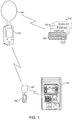
- FIG. 1 shows a system 100 in which a cardholder is alerted when an attempt is made to access a contactless smartcard 110.
- Contactless smartcards 110 (also referred to as “cards” or “smartcards”) store data which can be accessed wirelessly for conducting different types of transactions.
- cards 110 may include contactless credit cards, fare cards, building access cards, identification cards, etc.
- Card data may include account numbers, account balances, usage information, security codes, personal identifiers, and other potentially sensitive information.
- Smartcards 110 communicate with a card reader by modulating its magnetic field emissions according to a contactless smartcard communication (CSC) protocol.
- CSC contactless smartcard communication
- the cardholder waives a smartcard 110 in the vicinity of the card reader.
- the card reader accesses the stored data and may write updated information back to the card.
- POS point-of-sale
- the card reader accesses account information from the card and uses it to complete the purchase.
- skimming refers to a process by which card data is obtained either by accessing a card directly or by intercepting communications between a card and a card reader.
- Relay attacks involve conducting an unauthorized transaction using card data. Absent some form of protection, data stored by a contactless smartcard can be accessed in a relatively short period of time and without any warning to the cardholder.
- a first hacker utilizes a card reader 120 to generate polling signals with which to elicit a response from smartcards in its immediate vicinity.
- the polling signals may conform with a physical layer CSC protocol, such as that specified by the ISO 14443 standards, and may implement an anti-collision process for selecting among multiple responses.
- An antenna 130 coupled to card reader 120 directs the polling signal towards smartcards 110.
- the first hacker relays information from a responding smartcard 110 to a card emulator 140 operated by the second hacker.
- the card emulator 140 sends the relayed information via its antenna 130 to a vending machine 150 to initiate a transaction. Thereafter, card reader 120 and card emulator 140 pass information between the responding smartcard 110 and the vending machine 150 to complete the unauthorized transaction.
- data encryption will not protect the cardholder as the hackers need not know exactly what data is being transferred. Also, because there is no physical contact, the cardholder may be completely unaware that his or her private data is being used to conduct a fraudulent transaction. Consequently, the hackers may escape detection.
- Card protection device 160 alerts a cardholder to the unauthorized access and may temporarily block access to card data.
- card protection device 160 provides an audible and/or visual alert when access to card data is detected. This may include beeping, buzzing, vibrating, flashing, or any other manner of warning a cardholder that an attempt could be underway to access card data. The alert may provide the cardholder with an opportunity to move away from a suspicious area and/or to notify authorities of a suspicious person.
- Card protection device 160 can also disrupt access to card data. This may include attenuating magnetic field strength in the vicinity of smartcards 110. The attenuation can be based on card operating levels and/or timing requirements for accessing card data according to various CSC protocols. For example, in some embodiments, card protection device 160 absorbs energy from an external field thereby reducing the magnetic coupling with smartcards 110. The stored energy can be used to generate the alert thus avoiding the need for a battery or other power source. Attenuation can be based on smartcard operating levels and real-world operating scenarios. In other embodiments, the communication capability of a smartcard 110 may be temporarily disabled when an access attempt is detected pending authorization from the cardholder. For example, card operations may be suspended until a button is pressed or some other action is taken.
- Card protection device 160 can be a separate device which is carried with other cards 110.
- card protection device 160 is designed to be stacked with other cards and carried in a wallet or purse.
- Card protection device 160 may also be integrated with cards 110 to present a combined functionality. This can include, for example, sharing an antenna or other smartcard components and/or providing an integrated circuit having both smartcard communications and data protection capabilities. Many variations are possible within the scope of the present invention.
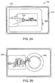
- FIGS. 2A-2B show one embodiment of a card protection device 160.
- Card protection device 160 can be sized according to the ISO/IEC 7810 standards for smartcards and may have a length of approximately 85.60 mm and a width of approximately 53.98 mm.
- a printed circuit element 210 provides support for device electronics 230.
- Printed circuit element 210 can be mounted to a flexible substrate to withstand the stress of being carried with smartcards 110 in a purse or wallet.
- a magnetic loop antenna 220 can be etched into or otherwise attached to printed circuit element 210 and adapted to receive magnetic field emissions in a frequency band associated with smartcard communications.
- magnetic loop antenna 220 may be optimized for 13.56 MHz communications used with ISO 14443 cards, or it may be adapted for use with other smartcard operating frequencies.
- Electronics 230 can be mounted to printed circuit element 210 and can respond to magnetic field emissions.
- electronics 230 include an energy storage element and control logic that is configured to absorb energy from ambient magnetic fields.
- a piezo-electric buzzer 240 may be coupled to electronics 230 to provide an audible alert when magnetic field emissions are detected.
- piezo-electric buzzer 240 is disposed in a Helmholz resonator cavity 250 which can be tuned to its piezo-resonance frequency. When the targeted emissions are detected, piezo-electric buzzer 240 emits an audible alert to warn a cardholder of a possible access attempt.
- FIG. 3 is a block diagram of an exemplary card protection device 300.
- Card protection device 300 can be as described in FIGS. 1-2 and some or all of elements 310-330 can be included as part of device electronics 230.
- antenna 220 is shown coupled to a tuning circuit 310.
- Antenna 220 can be a magnetic loop antenna having between 2-5 turns. With an etched antenna, the traces are preferably at least 1.5 mm thick to reduce impedance and improve magnetic field coupling.
- Tuning circuit 310 can be matched with antenna 220 and configured for sensitivity to magnetic field emissions used with contactless smartcards 110.
- tuning circuit 310 operates with a resonant frequency slightly higher than the load-modulation capabilities of conventional smartcards.
- tuning circuit 310 may have a resonant frequency of between 14 MHz - 18 MHz for use with 13.56 MHz smartcards such as those conforming to ISO 14443 standards.
- a detector circuit (“detector”) 320 is coupled to tuning circuit 310.
- Detector 320 can be configured to detect magnetic field emissions and to store electrical energy associated with such emissions.
- the sensitivity of detector 320 can be based on the operating parameters of smartcards 110. For example, ISO 14443 standards require compliant cards to operate at a minimum field strength of 1.5 A/m. Testing with commercially available cards suggests that many function at levels that are below standards and some may respond to field strengths as low as 0.6 A/m. Accordingly, detector circuit 320 may implement a detection threshold of 0.6 A/m (or lower). Magnetic fields below the detection threshold may be disregarded as spurious and likely incapable of accessing smartcard data. On the other hand, card protection device 300 can respond automatically to magnetic fields that exceed the detection threshold and which therefore could be used to access card data.
- Detector circuit 320 may also include an energy storage element for absorbing electrical energy associated with the field emissions.
- card protection device 300 uses the stored electrical energy as a source of power. This may eliminate the need for batteries and can reduce overall size and manufacturing costs.
- Detector circuit 320 can be configured to store electrical energy from the magnetic field for a period that is related to smartcard operating capabilities. The period can be based on the time required to complete a smartcard transaction, the time required to access data from smartcard memory, the time required to authenticate card credentials, etc.
- Detector circuit 320 can be configured to store energy from the magnetic field for a time sufficient to provide an alert to the cardholder before such a transaction is completed. By strongly coupling with the magnetic field during a protection interval, card protection device 300 can attenuate the field strength and increase the difficulty of accessing data from nearby smartcards. After the protection interval, detector circuit 320 can optionally discontinue field attenuation. For example, when the cardholder presents his or her wallet to a card reader, the detector circuit 320 can suspend field attenuation after a warning is given.
- Detector circuit 320 is coupled to an alerting circuit 330.
- Alerting circuit 330 generates an output signal which drives an audio/visual alerting element 340 such as piezo-electric buzzer 240, one or more light-emitting diodes (LEDs), and the like.
- Alerting circuit 330 can be configured to vary a rate of the output signal according to the strength of the detected magnetic field emissions. In some embodiments, the strength of magnetic field emissions is determined based on the rate at which electrical energy is stored by the storage element. When a strong magnetic field is encountered, the storage element of detector circuit 320 may charge quickly whereas, in the presence of a weak magnetic field, the storage element may charge slowly.
- Alerting circuit 330 can vary a tone, intensity, or beep-rate of the audible alert based on the charging rate. In this way, the cardholder can be warned when approaching an area in which suspicious fields are present.
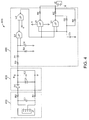
- FIG. 4 is a schematic diagram showing aspects of exemplary card protection electronics 400.
- Electronics 400 can be used with the card protection devices 160, 300 and are divided into functional groups 410, 420, 430 for purposes of discussion. It will be recognized, however, that electronics 400 are illustrative only and that different components and/or circuit blocks may be used within the scope of the present invention.
- Block 410 includes magnetic loop antenna (J1) and tuning circuit which is sensitive to magnetic field emissions in a frequency band used for smartcard communications.
- J1 magnetic loop antenna
- tuning circuit which is sensitive to magnetic field emissions in a frequency band used for smartcard communications.
- values of R1, R2, and C1 can be determined to form a resonance circuit sensitive that is optimized for receiving emissions in the targeted frequency band.
- the resonance circuit for example, can be configured for sensitivity to 13.56 MHz emissions used with ISO 14443 cards.
- block 420 The output of block 410 is connected to block 420 which can act as a detector circuit.
- block 420 includes a diode rectifier arrangement D1, Z1 and an energy storage capacitor C2.
- the rectifier diodes charge storage capacitor C2 with energy derived from the magnetic field emissions. Energy from storage capacitor C2 can be used to drive an alerting circuitry in block 430.
- block 430 includes a plurality of logic elements arranged so as to provide a variable driving signal to an audible alert device (J2).
- the driving signal can produce an audible alert which varies according to the charge rate of storage capacitor C2.
- the value of storage capacitor C2 and the impedance of the resonance circuit 410 may be used to vary a charging time of the detector circuit 430.
- the charging time of the detector circuit in combination with a power consumption of the audible alert element J2, determines how much the magnetic field will be loaded when the storage capacitor C2 is fully charged.
- component values of R1, R2, C1, and C2 may be selected to vary the amount and duration by which the magnetic field is attenuated according to card operating requirements and access times as previously discussed.
- FIG. 5 shows exemplary control logic for changing a magnetic field loading characteristic of card protection electronics 400.
- the input of a control logic element 510 is coupled to the storage capacitor C2 of block 420.
- the output of control logic 510 operates a switching element SW1 which is added in parallel with resistor R9 and coupled with the diode D1 and storage capacitor C2 as shown in blocks 410, 420.
- control logic 510 opens switching element SW1. This, in turn, reduces a load on the magnetic field and may facilitate the interaction of collocated smartcards 110 with a card reader.
- Component values of R1, R2, and C2 are selected such that the charge on storage capacitor C2 is sufficient to drive audible alert J2 without discharging by more than approximately 10%.
- the magnetic field can be attenuated for a time sufficient to provide an audible alert and then reduced once the alert is given. This, in turn, allows the cardholder to use a protected smartcard 110 to complete a transaction.
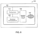
- FIG. 6 shows another embodiment of a card protection device 600.
- Card protection device 600 adds protection capabilities to a conventional smartcard device.
- a tuning circuit 610 is coupled to a magnetic loop antenna 220.
- the tuning circuit can be as described in connection with FIG. 3 and is configured to detect magnetic field emissions in a frequency band used for smartcard communications.
- Tuning circuit 610 is also coupled to a smartcard communications module 620 and a detector/alerting circuit 630 ("detector").
- Communications module 620 can be an integrated circuit or other component used with smartcards 110 to control magnetic field load-modulation.
- communication module 620 can be an application-specific integrated circuit (ASIC) such as those used in contactless credit cards, fare cards, bank cards, access control cards, and the like.
- Detector/alerting circuit 630 is coupled to an alerting device 640 such as the piezo-electric buzzer 240 shown in FIG. 2 . With this arrangement, the magnetic loop antenna 220 and tuning circuit 610 are shared by smartcard communications module 620 and protection electronics 630, 640.
- tuning circuit 610 passes a current induced by the external magnetic field emissions to detector 630.
- Detector 630 can implement a detection threshold related to the operating characteristics of smartcard communications module 620. For example, when smartcard communications module 620 is used with transit systems, such as a MiFare card, the detection threshold may be set to 1.0 A/m, 0.6 A/m, or some other value related to its minimum operating level.
- detector 630 outputs an alerting signal which drives alerting device 640.
- detector 630 can be powered by energy from the external magnetic field emissions and may vary the alerting signal according to field strength, charge rate, or other factors.
- detector 630 can implement a protection threshold for attenuating the magnetic field based on the communications protocol of smartcard communications module 620.
- detector 630 may include the protection electronics of FIG. 4 and the control logic of FIG. 5 configured so as to strongly attenuate magnetic field strength for a period that is based on the time required to conduct a ticketing transaction or other payment using the card data.
- MiFare cards for example, by disrupting the field for approximately 50 ms, it may be possible to frustrate the handshaking process and require a hacker to repeat a command sequence or initiate a new transaction.
- detector 630 can raise an alarm at alerting device 640 to warn the cardholder of an authorized attempt to access card data. After the protection interval, or when an alarm having a predetermined duration has been given, the attenuation can be suspended by operation of control logic 510 or in some other manner.
- FIG. 7 shows an embodiment of a smartcard device 700.
- Smartcard 700 integrates protection and alerting functions with conventional smartcard communications.
- a tuning circuit 710 is coupled to a magnetic loop antenna 220 disposed on a card substrate.
- Tuning circuit 710 can be as described in connection with FIG. 3 and is configured to detect magnetic field emissions in a frequency band used for smartcard communications.
- Tuning circuit 710 is also coupled to modules 720.
- Modules 720 can include one or more application specific integrated circuits and supporting electronics.
- the ASICs can include protocol modules 740 used for exchanging commands and data with card readers.
- the ASICs may also include registers and the like for storing account numbers and other types of card data used to perform transactions.
- One or more protection modules 730 can be coupled to and interact with the protocol modules 740 to enable a fine grained control over card-based communications.
- protection module 730 can be configured to detect magnetic field emissions and to generate an alerting signal which drives an audible and/or visual alert element 750.
- the alert element 750 can be a buzzer, one or more light emitting diodes (LEDs), and the like.
- protection module 730 can analyze the magnetic field emissions to reduce the number of false alarms. For example, RF fields that do not conform with a particular CSC protocol can be ignored without raising an alarm.
- protection module 730 may disable operation of protocol module 740 to prevent access to card data.
- the card may remain in the first operating mode with communications disabled until a user input is received.
- an OK button 760 is provided to reset operation of the protocol modules 740 when a suspicious access attempt is detected.
- protection module 730 clears the alarm condition and smartcard 700 transitions to a second operating mode in which the cardholder can proceed with an authorized transaction.
- card protection device 700 includes one or more additional storage elements 770.
- the additional storage element 770 can include information such as a positive list used by protection module 730 to allow access to card data.
- the positive list 770 may identify card readers that are allowed to communicate with the card.
- protection module 730 can compare a device identifier of the card reader to the positive list 770. If the identifier is not found in the positive list 770, access to card data can be prevented and protection module 730 can enter the first operating mode and begin generating an alerting signal. In addition to an audible alert, an LED or other indicator of card protection device 700 can be used to signal that fraudulent access was detected and blocked. The cardholder may then be required to press OK button 760 to reset device operation.
- FIG. 8 is an exemplary process 800 such as can be carried out by a card protection device.
- Process 800 may be implemented with protection electronics such as shown in FIG. 3 or FIG. 4 .
- process 800 can be performed by one or more modules such as the application specific integrated circuits described in connection with FIG. 7 , or in some other manner.
- magnetic field emissions are detected.
- the magnetic field emissions can be broad spectrum or in a frequency band used for smartcard communications.
- the card protection device stores energy associated with emissions.
- the stored energy can be used to power the card protection device and can provide an indication of the strength of the magnetic field.
- field energy is stored in a capacitor and a charge or voltage level of the capacitor is monitored for alerting. If the charge or voltage level does not exceed a threshold related to card operating levels, the card protection device may disregard the field and suppress alerting functions.
- the stored energy can be used to generate an audible and/or visual alert.
- the alert may be varied based on field strength which can provide an indication of the cardholder's proximity to the transmitter. For example, the tone or beep-rate of an audible signal may change as the cardholder moves in relation to a transmitter.
- the alert is expected and can be ignored. However, when a hacker attempts to access card data, the alert serves as a warning to the cardholder.
- the card protection device varies the amount by which the magnetic field is attenuated. This can involve varying an impedance of the protection circuit such that the magnetic field is heavily loaded for an interval while an alert is sounded. Following the alert, the impedance may be changed so as to enable normal functioning of smartcards. Loading the magnetic field may increase the power required to activate nearby smartcards and potentially frustrate a hacker's attempt to access card data.
- the duration of the loading interval may be based on the time required to access card data under real-world conditions. Components values of the protection electronics may be selected accordingly. For example, the loading duration may be set to approximately 50 ms assuming a field strength of 2 A/m at a range of 8 - 30 cms.
- the card protection device may reduce or discontinue loading the field to permit normal card operation.
- control logic can be used to adjust device impedance so that data can be accessed normally from nearby cards. Many variations in components and control logic functioning can be made to adapt the protection device to card operating characteristics within the scope of the present invention.
- FIG. 9 is an exemplary process 900 such as can be carried out by a smartcard device.
- Process 900 may be implemented by modules 720 as described in connection with FIG. 7 , or other embodiments in which card alerting and protection is integrated with communications and data access capabilities.
- a magnetic field is detected. Detecting the field may be based initially on field strength. For example, processing may continue to block 910 only when the field strength exceeds the minimum operating level of a conventional smartcard device.
- the smartcard device determines whether the field is appropriate for communicating with a smartcard. This may include determining whether frequency, amplitude, modulation, and other field characteristics comply with smartcard communication protocols. Emissions which are incompatible with smartcard operation can be disregarded to reduce the likelihood of false alarms.
- a smartcard protocol When a smartcard protocol is detected, it can be demodulated and analyzed at block 915. For example, before access to card data is permitted, one or more protocol modules of an integrated circuit may demodulate the magnetic field to obtain an identifier associated with the card reader. Using the identifier, a determination is made at block 920 as to whether the card reader is found on a list of valid devices. If the card reader is found on the positive list, block 945, access to card data is permitted and the transaction can continue. For example, when the identifier is validated by a positive list, a transition to the second operating mode may occur and normal card-based authentication and encryption routines can be allowed to proceed.
- an audible and/or visual alert can be generated. The alert may continue, block 940, until operation of the smartcard device is reset at block 935.
Landscapes
- Physics & Mathematics (AREA)
- Engineering & Computer Science (AREA)
- Electromagnetism (AREA)
- Computer Hardware Design (AREA)
- Computer Security & Cryptography (AREA)
- General Engineering & Computer Science (AREA)
- Microelectronics & Electronic Packaging (AREA)
- General Physics & Mathematics (AREA)
- Theoretical Computer Science (AREA)
- Near-Field Transmission Systems (AREA)
- Credit Cards Or The Like (AREA)
Claims (11)
- Kartenschutzvorrichtung (160, 300, 600, 700), umfassend:eine Antenne (220) mit einer Abstimmschaltung (310, 610, 710), die auf Magnetfeldemissionen in einem Frequenzband anspricht, das kontaktlosen Smartcard-Kommunikationen zugeordnet ist;eine Detektorschaltung (230, 320, 630, 730), die mit der Antenne gekoppelt und ausgelegt ist, um den Magnetfeldemissionen zugeordnete Energie zu speichern;eine Warnschaltung (240, 330, 630, 750), die ausgelegt ist, um als Reaktion auf Magnetfeldemissionen unter Nutzen der gespeicherten Energie der Detektorschaltung eine akustische und/oder optische Warnung vorzusehen; undeine Schaltungsanordnung, um die Energie der Magnetfeldemissionen über einen Zeitraum, der gemäß Smartcard-Betriebseigenschaften ermittelt wird, zu dämpfen,dadurch gekennzeichnet, dassdie Warnschaltung ausgelegt ist, um die akustische und/oder optische Warnung gemäß einer Stärke der Magnetfeldemissionen zu ändern.
- Kartenschutzvorrichtung nach Anspruch 1, wobei die Antenne eine Magnetschleife umfasst und die Abstimmschaltung eine Resonanzfrequenz aufweist, die an das Frequenzband der Smartcard-Kommunikationen angepasst ist.
- Kartenschutzvorrichtung nach Anspruch 1, wobei der Zeitraum auf einer Zeit beruht, die zum Zugreifen auf Daten von einer kontaktlosen Smartcard gemäß einem Kommunikationsprotokoll erforderlich ist.
- Kartenschutzvorrichtung nach Anspruch 1, wobei die Warnschaltung ausgelegt ist, um die akustische und/oder optische Warnung als Reaktion darauf, dass die Magnetfeldemissionen einen Schwellenwert übersteigen, vorzusehen.
- Kartenschutzvorrichtung nach Anspruch 1, wobei der Schwellenwert auf einem Pegel der gespeicherten Energie beruht.
- Kartenschutzvorrichtung nach Anspruch 1, wobei die Warnschaltung einen piezoelektrischen Summer umfasst.
- Kartenschutzvorrichtung nach Anspruch 1, wobei die Warnschaltung ausgelegt ist, um die akustische und/oder optische Warnung gemäß einer Rate zu ändern, bei der die dem Magnetfeld zugeordnete Energie gespeichert wird.
- Verfahren (800) zum Detektieren eines Zugriffs auf eine kontaktlose Smartcard, umfassend:Detektieren von Magnetfeldemissionen (810) in einem Frequenzband, das Smartcard-Kommunikationen zugeordnet ist, an einer Detektionsvorrichtung;Speichern einer elektrischen Energie (820), die den Magnetfeldemissionen zugeordnet ist, an der Detektionsvorrichtung;Erzeugen (830) einer akustischen und/oder optischen Warnung als Reaktion auf die Magnetfeldemissionen unter Nutzen der gespeicherten elektrischen Energie;Dämpfen der Magnetfeldemissionen (840) über eine Zeit, die mit einem kontaktlosen Smartcard-Kommunikationsprotokoll in Verbindung steht;gekennzeichnet durchÄndern der akustischen und/oder optischen Warnung beruhend auf einer Stärke der Magnetfeldemissionen.
- Verfahren nach Anspruch 8, wobei das kontaktlose Smartcard-Kommunikationsprotokoll durch die Normen ISO 1443 spezifiziert ist und die Zeit etwa 50 Millisekunden beträgt.
- Verfahren nach Anspruch 8, wobei das Dämpfen der Stärke der Magnetfeldemissionen das Ändern einer Impedanz der Detektionsvorrichtung umfasst.
- Verfahren nach Anspruch 8, weiterhin umfassend:Detektieren eines Werts der Magnetfeldemissionen; undErzeugen der akustischen und/oder optischen Warnung als Reaktion darauf, dass der Wert der Magnetfeldemissionen einen Schwellenwert übersteigt.
Applications Claiming Priority (3)
| Application Number | Priority Date | Filing Date | Title |
|---|---|---|---|
| US15147509P | 2009-02-10 | 2009-02-10 | |
| US12/702,170 US8902073B2 (en) | 2009-02-10 | 2010-02-08 | Smartcard protection device |
| PCT/US2010/023616 WO2010093623A1 (en) | 2009-02-10 | 2010-02-09 | Smartcard protection device |
Publications (2)
| Publication Number | Publication Date |
|---|---|
| EP2396751A1 EP2396751A1 (de) | 2011-12-21 |
| EP2396751B1 true EP2396751B1 (de) | 2016-08-10 |
Family
ID=42539979
Family Applications (1)
| Application Number | Title | Priority Date | Filing Date |
|---|---|---|---|
| EP10704462.0A Not-in-force EP2396751B1 (de) | 2009-02-10 | 2010-02-09 | Smartcard-schutzvorrichtung |
Country Status (5)
| Country | Link |
|---|---|
| US (1) | US8902073B2 (de) |
| EP (1) | EP2396751B1 (de) |
| AU (1) | AU2010213888B2 (de) |
| CA (1) | CA2752104C (de) |
| WO (1) | WO2010093623A1 (de) |
Families Citing this family (7)
| Publication number | Priority date | Publication date | Assignee | Title |
|---|---|---|---|---|
| DE102013014187A1 (de) * | 2013-08-26 | 2015-02-26 | Giesecke & Devrient Gmbh | Verfahren und Vorrichtung zur Übertragung einer Information |
| AT515401B1 (de) * | 2014-02-03 | 2016-04-15 | Seibersdorf Labor Gmbh | Abschirmelement zum Anbringen auf einem Gegenstand |
| ES2982728T3 (es) | 2016-03-01 | 2024-10-17 | James Carey | Protección de los datos personales contenidos en un dispositivo habilitado para RFID |
| CN105795643A (zh) * | 2016-05-23 | 2016-07-27 | 任海拢 | 一种钱包和防止钱包被盗刷的方法 |
| WO2018169522A1 (en) * | 2017-03-15 | 2018-09-20 | Visa International Service Association | Method and system for relay attack detection |
| US10977539B1 (en) * | 2019-12-20 | 2021-04-13 | Capital One Services, Llc | Systems and methods for use of capacitive member to prevent chip fraud |
| US12277543B2 (en) * | 2022-08-03 | 2025-04-15 | Capital One Services, Llc | Tone verification of a physical card |
Family Cites Families (27)
| Publication number | Priority date | Publication date | Assignee | Title |
|---|---|---|---|---|
| CA1110341A (en) * | 1977-08-19 | 1981-10-06 | John D. Mccann | Marker tag for a detection system |
| US5103209A (en) * | 1989-01-09 | 1992-04-07 | Checkpoint Systems, Inc. | Electronic article surveillance system with improved differentiation |
| GB9821046D0 (en) * | 1998-09-28 | 1998-11-18 | Whitesmith Howard W | Detection system |
| WO2001022359A1 (fr) | 1999-09-22 | 2001-03-29 | Fujitsu Limited | Carte a circuit integre sans contact |
| FI20002882L (fi) * | 2000-12-29 | 2002-06-30 | Nokia Corp | Järjestely antennin sovittamiseksi |
| EP1380020A4 (de) * | 2001-03-30 | 2006-08-30 | Augmentech Inc | Patienteninkontinenz-/positionsüberwachungsvorrichtung und verfahren und verwendung dafür |
| FR2831305B1 (fr) * | 2001-10-23 | 2004-01-30 | Inside Technologies | Circuit integre sans contact comprenant des moyens d'identification automatique de trame |
| US6744366B2 (en) * | 2002-04-04 | 2004-06-01 | Hoton How | Method and apparatus of obtaining security tag operation using local magnetic marker |
| JP2005045557A (ja) * | 2003-07-22 | 2005-02-17 | Sony Corp | 通信装置 |
| FR2871312B1 (fr) * | 2004-06-03 | 2006-08-11 | St Microelectronics Sa | Modulation de charge dans un transpondeur electromagnetique |
| JP5100966B2 (ja) | 2005-01-17 | 2012-12-19 | ソニーモバイルコミュニケーションズ株式会社 | 非接触型近距離無線通信装置、携帯電話端末 |
| EP1891748A1 (de) * | 2005-06-14 | 2008-02-27 | Nokia Corporation | Etikettmultiplikation |
| US7522905B2 (en) * | 2005-06-24 | 2009-04-21 | Visa U.S.A. Inc. | Apparatus and method for preventing wireless interrogation of portable consumer devices |
| US7586413B2 (en) | 2005-09-01 | 2009-09-08 | Assa Abloy Ab | Human feedback using parasitic power harvesting of RFID tags |
| US7889056B2 (en) * | 2005-10-31 | 2011-02-15 | Curio, Ltd. | RFID protection system, device, combination, and related methods |
| US8102243B2 (en) * | 2005-10-31 | 2012-01-24 | Curio Ltd. | RFID protection device, and related methods |
| DE102006008345B3 (de) | 2006-02-21 | 2007-08-23 | Bundesdruckerei Gmbh | Sicherheits- und/oder Wertdokument |
| US7821402B2 (en) * | 2006-05-05 | 2010-10-26 | Quality Electrodynamics | IC tags/RFID tags for magnetic resonance imaging applications |
| CN101416201B (zh) * | 2006-05-15 | 2012-05-09 | 国际商业机器公司 | 使用无源rfid标签定位对象的方法和系统 |
| US7635089B2 (en) * | 2006-07-03 | 2009-12-22 | Identity Stronghold, Llc | Device for shielding reading of a contactless smartcard |
| US7764046B2 (en) * | 2006-08-31 | 2010-07-27 | Semiconductor Energy Laboratory Co., Ltd. | Power storage device and semiconductor device provided with the power storage device |
| US7965186B2 (en) | 2007-03-09 | 2011-06-21 | Corning Cable Systems, Llc | Passive RFID elements having visual indicators |
| US7992779B2 (en) * | 2007-09-10 | 2011-08-09 | Mastercard International, Inc. | Method for use in association with identification token and apparatus including identification token |
| US20090096580A1 (en) * | 2007-10-11 | 2009-04-16 | Nokia Corporation | Secure authentication |
| US20090152364A1 (en) | 2007-12-12 | 2009-06-18 | Spivey Technologies, Llc | Rfid card with piezoelectric element |
| US8222996B2 (en) * | 2007-12-31 | 2012-07-17 | Intel Corporation | Radio frequency identification tags adapted for localization and state indication |
| FR2929430B1 (fr) | 2008-03-31 | 2010-10-22 | Ask Sa | Objet portable sans contact capable d'apporter une indication sur la performance d'un lecteur sans contact |
-
2010
- 2010-02-08 US US12/702,170 patent/US8902073B2/en not_active Expired - Fee Related
- 2010-02-09 CA CA2752104A patent/CA2752104C/en not_active Expired - Fee Related
- 2010-02-09 AU AU2010213888A patent/AU2010213888B2/en not_active Ceased
- 2010-02-09 WO PCT/US2010/023616 patent/WO2010093623A1/en not_active Ceased
- 2010-02-09 EP EP10704462.0A patent/EP2396751B1/de not_active Not-in-force
Also Published As
| Publication number | Publication date |
|---|---|
| AU2010213888B2 (en) | 2015-01-22 |
| US20100201534A1 (en) | 2010-08-12 |
| EP2396751A1 (de) | 2011-12-21 |
| WO2010093623A1 (en) | 2010-08-19 |
| CA2752104A1 (en) | 2010-08-19 |
| AU2010213888A1 (en) | 2011-09-01 |
| US8902073B2 (en) | 2014-12-02 |
| CA2752104C (en) | 2017-07-11 |
Similar Documents
| Publication | Publication Date | Title |
|---|---|---|
| EP2396751B1 (de) | Smartcard-schutzvorrichtung | |
| CA2668333C (en) | Device for protecting contactless communication objects against fraud | |
| JP2007512611A (ja) | タグ及びスマートカードのための妨害器 | |
| JP6875401B2 (ja) | バイオメトリックデバイス | |
| EP2392078B1 (de) | Smartcard-protokollsender | |
| EP2717553A1 (de) | Tragbare Nahfeldkommunikationsvorrichtung | |
| US11734524B2 (en) | Protection of personal data contained on an RFID-enabled device | |
| EP3332359A1 (de) | Sicherheitsgeschützte passive rfid-vorrichtung | |
| US20190065716A1 (en) | Attack resistant biometric authorised device | |
| US10628722B2 (en) | Method and apparatus to enhance the security of contact-less cards | |
| EP3453117B1 (de) | Tragbare vorrichtung mit integriertem rfid- oder nfc-chipsatz | |
| US20230334131A1 (en) | Biometrically protected device | |
| Grillmayer | Radio-Frequency Identification-Overview | |
| Chernenko et al. | TECHNOLOGY AND DEVELOPMENT PROSPECTS OF BANK CARDS | |
| HK1233739A1 (en) | Security protected rfid device |
Legal Events
| Date | Code | Title | Description |
|---|---|---|---|
| PUAI | Public reference made under article 153(3) epc to a published international application that has entered the european phase |
Free format text: ORIGINAL CODE: 0009012 |
|
| 17P | Request for examination filed |
Effective date: 20110909 |
|
| AK | Designated contracting states |
Kind code of ref document: A1 Designated state(s): AT BE BG CH CY CZ DE DK EE ES FI FR GB GR HR HU IE IS IT LI LT LU LV MC MK MT NL NO PL PT RO SE SI SK SM TR |
|
| DAX | Request for extension of the european patent (deleted) | ||
| 17Q | First examination report despatched |
Effective date: 20131205 |
|
| GRAP | Despatch of communication of intention to grant a patent |
Free format text: ORIGINAL CODE: EPIDOSNIGR1 |
|
| INTG | Intention to grant announced |
Effective date: 20160308 |
|
| GRAS | Grant fee paid |
Free format text: ORIGINAL CODE: EPIDOSNIGR3 |
|
| GRAA | (expected) grant |
Free format text: ORIGINAL CODE: 0009210 |
|
| AK | Designated contracting states |
Kind code of ref document: B1 Designated state(s): AT BE BG CH CY CZ DE DK EE ES FI FR GB GR HR HU IE IS IT LI LT LU LV MC MK MT NL NO PL PT RO SE SI SK SM TR |
|
| REG | Reference to a national code |
Ref country code: GB Ref legal event code: FG4D |
|
| REG | Reference to a national code |
Ref country code: CH Ref legal event code: EP Ref country code: AT Ref legal event code: REF Ref document number: 819628 Country of ref document: AT Kind code of ref document: T Effective date: 20160815 |
|
| REG | Reference to a national code |
Ref country code: IE Ref legal event code: FG4D |
|
| REG | Reference to a national code |
Ref country code: DE Ref legal event code: R096 Ref document number: 602010035325 Country of ref document: DE |
|
| REG | Reference to a national code |
Ref country code: LT Ref legal event code: MG4D |
|
| REG | Reference to a national code |
Ref country code: NL Ref legal event code: MP Effective date: 20160810 |
|
| REG | Reference to a national code |
Ref country code: AT Ref legal event code: MK05 Ref document number: 819628 Country of ref document: AT Kind code of ref document: T Effective date: 20160810 |
|
| PG25 | Lapsed in a contracting state [announced via postgrant information from national office to epo] |
Ref country code: HR Free format text: LAPSE BECAUSE OF FAILURE TO SUBMIT A TRANSLATION OF THE DESCRIPTION OR TO PAY THE FEE WITHIN THE PRESCRIBED TIME-LIMIT Effective date: 20160810 Ref country code: NL Free format text: LAPSE BECAUSE OF FAILURE TO SUBMIT A TRANSLATION OF THE DESCRIPTION OR TO PAY THE FEE WITHIN THE PRESCRIBED TIME-LIMIT Effective date: 20160810 Ref country code: NO Free format text: LAPSE BECAUSE OF FAILURE TO SUBMIT A TRANSLATION OF THE DESCRIPTION OR TO PAY THE FEE WITHIN THE PRESCRIBED TIME-LIMIT Effective date: 20161110 Ref country code: LT Free format text: LAPSE BECAUSE OF FAILURE TO SUBMIT A TRANSLATION OF THE DESCRIPTION OR TO PAY THE FEE WITHIN THE PRESCRIBED TIME-LIMIT Effective date: 20160810 Ref country code: IT Free format text: LAPSE BECAUSE OF FAILURE TO SUBMIT A TRANSLATION OF THE DESCRIPTION OR TO PAY THE FEE WITHIN THE PRESCRIBED TIME-LIMIT Effective date: 20160810 Ref country code: FI Free format text: LAPSE BECAUSE OF FAILURE TO SUBMIT A TRANSLATION OF THE DESCRIPTION OR TO PAY THE FEE WITHIN THE PRESCRIBED TIME-LIMIT Effective date: 20160810 Ref country code: IS Free format text: LAPSE BECAUSE OF FAILURE TO SUBMIT A TRANSLATION OF THE DESCRIPTION OR TO PAY THE FEE WITHIN THE PRESCRIBED TIME-LIMIT Effective date: 20161210 |
|
| PG25 | Lapsed in a contracting state [announced via postgrant information from national office to epo] |
Ref country code: GR Free format text: LAPSE BECAUSE OF FAILURE TO SUBMIT A TRANSLATION OF THE DESCRIPTION OR TO PAY THE FEE WITHIN THE PRESCRIBED TIME-LIMIT Effective date: 20161111 Ref country code: ES Free format text: LAPSE BECAUSE OF FAILURE TO SUBMIT A TRANSLATION OF THE DESCRIPTION OR TO PAY THE FEE WITHIN THE PRESCRIBED TIME-LIMIT Effective date: 20160810 Ref country code: PL Free format text: LAPSE BECAUSE OF FAILURE TO SUBMIT A TRANSLATION OF THE DESCRIPTION OR TO PAY THE FEE WITHIN THE PRESCRIBED TIME-LIMIT Effective date: 20160810 Ref country code: AT Free format text: LAPSE BECAUSE OF FAILURE TO SUBMIT A TRANSLATION OF THE DESCRIPTION OR TO PAY THE FEE WITHIN THE PRESCRIBED TIME-LIMIT Effective date: 20160810 Ref country code: LV Free format text: LAPSE BECAUSE OF FAILURE TO SUBMIT A TRANSLATION OF THE DESCRIPTION OR TO PAY THE FEE WITHIN THE PRESCRIBED TIME-LIMIT Effective date: 20160810 Ref country code: PT Free format text: LAPSE BECAUSE OF FAILURE TO SUBMIT A TRANSLATION OF THE DESCRIPTION OR TO PAY THE FEE WITHIN THE PRESCRIBED TIME-LIMIT Effective date: 20161212 Ref country code: SE Free format text: LAPSE BECAUSE OF FAILURE TO SUBMIT A TRANSLATION OF THE DESCRIPTION OR TO PAY THE FEE WITHIN THE PRESCRIBED TIME-LIMIT Effective date: 20160810 |
|
| PG25 | Lapsed in a contracting state [announced via postgrant information from national office to epo] |
Ref country code: EE Free format text: LAPSE BECAUSE OF FAILURE TO SUBMIT A TRANSLATION OF THE DESCRIPTION OR TO PAY THE FEE WITHIN THE PRESCRIBED TIME-LIMIT Effective date: 20160810 Ref country code: RO Free format text: LAPSE BECAUSE OF FAILURE TO SUBMIT A TRANSLATION OF THE DESCRIPTION OR TO PAY THE FEE WITHIN THE PRESCRIBED TIME-LIMIT Effective date: 20160810 |
|
| PGFP | Annual fee paid to national office [announced via postgrant information from national office to epo] |
Ref country code: DE Payment date: 20170227 Year of fee payment: 8 |
|
| REG | Reference to a national code |
Ref country code: DE Ref legal event code: R097 Ref document number: 602010035325 Country of ref document: DE |
|
| PG25 | Lapsed in a contracting state [announced via postgrant information from national office to epo] |
Ref country code: SM Free format text: LAPSE BECAUSE OF FAILURE TO SUBMIT A TRANSLATION OF THE DESCRIPTION OR TO PAY THE FEE WITHIN THE PRESCRIBED TIME-LIMIT Effective date: 20160810 Ref country code: CZ Free format text: LAPSE BECAUSE OF FAILURE TO SUBMIT A TRANSLATION OF THE DESCRIPTION OR TO PAY THE FEE WITHIN THE PRESCRIBED TIME-LIMIT Effective date: 20160810 Ref country code: SK Free format text: LAPSE BECAUSE OF FAILURE TO SUBMIT A TRANSLATION OF THE DESCRIPTION OR TO PAY THE FEE WITHIN THE PRESCRIBED TIME-LIMIT Effective date: 20160810 Ref country code: BG Free format text: LAPSE BECAUSE OF FAILURE TO SUBMIT A TRANSLATION OF THE DESCRIPTION OR TO PAY THE FEE WITHIN THE PRESCRIBED TIME-LIMIT Effective date: 20161110 Ref country code: DK Free format text: LAPSE BECAUSE OF FAILURE TO SUBMIT A TRANSLATION OF THE DESCRIPTION OR TO PAY THE FEE WITHIN THE PRESCRIBED TIME-LIMIT Effective date: 20160810 Ref country code: BE Free format text: LAPSE BECAUSE OF FAILURE TO SUBMIT A TRANSLATION OF THE DESCRIPTION OR TO PAY THE FEE WITHIN THE PRESCRIBED TIME-LIMIT Effective date: 20160810 |
|
| PLBE | No opposition filed within time limit |
Free format text: ORIGINAL CODE: 0009261 |
|
| STAA | Information on the status of an ep patent application or granted ep patent |
Free format text: STATUS: NO OPPOSITION FILED WITHIN TIME LIMIT |
|
| 26N | No opposition filed |
Effective date: 20170511 |
|
| PGFP | Annual fee paid to national office [announced via postgrant information from national office to epo] |
Ref country code: GB Payment date: 20170427 Year of fee payment: 8 |
|
| PG25 | Lapsed in a contracting state [announced via postgrant information from national office to epo] |
Ref country code: SI Free format text: LAPSE BECAUSE OF FAILURE TO SUBMIT A TRANSLATION OF THE DESCRIPTION OR TO PAY THE FEE WITHIN THE PRESCRIBED TIME-LIMIT Effective date: 20160810 |
|
| PG25 | Lapsed in a contracting state [announced via postgrant information from national office to epo] |
Ref country code: MC Free format text: LAPSE BECAUSE OF FAILURE TO SUBMIT A TRANSLATION OF THE DESCRIPTION OR TO PAY THE FEE WITHIN THE PRESCRIBED TIME-LIMIT Effective date: 20160810 |
|
| REG | Reference to a national code |
Ref country code: CH Ref legal event code: PL |
|
| PG25 | Lapsed in a contracting state [announced via postgrant information from national office to epo] |
Ref country code: LI Free format text: LAPSE BECAUSE OF NON-PAYMENT OF DUE FEES Effective date: 20170228 Ref country code: CH Free format text: LAPSE BECAUSE OF NON-PAYMENT OF DUE FEES Effective date: 20170228 |
|
| REG | Reference to a national code |
Ref country code: FR Ref legal event code: ST Effective date: 20171031 |
|
| PG25 | Lapsed in a contracting state [announced via postgrant information from national office to epo] |
Ref country code: LU Free format text: LAPSE BECAUSE OF NON-PAYMENT OF DUE FEES Effective date: 20170209 |
|
| PG25 | Lapsed in a contracting state [announced via postgrant information from national office to epo] |
Ref country code: FR Free format text: LAPSE BECAUSE OF NON-PAYMENT OF DUE FEES Effective date: 20170228 |
|
| REG | Reference to a national code |
Ref country code: DE Ref legal event code: R119 Ref document number: 602010035325 Country of ref document: DE |
|
| PG25 | Lapsed in a contracting state [announced via postgrant information from national office to epo] |
Ref country code: MT Free format text: LAPSE BECAUSE OF NON-PAYMENT OF DUE FEES Effective date: 20170209 |
|
| GBPC | Gb: european patent ceased through non-payment of renewal fee |
Effective date: 20180209 |
|
| PG25 | Lapsed in a contracting state [announced via postgrant information from national office to epo] |
Ref country code: DE Free format text: LAPSE BECAUSE OF NON-PAYMENT OF DUE FEES Effective date: 20180901 |
|
| PG25 | Lapsed in a contracting state [announced via postgrant information from national office to epo] |
Ref country code: GB Free format text: LAPSE BECAUSE OF NON-PAYMENT OF DUE FEES Effective date: 20180209 |
|
| REG | Reference to a national code |
Ref country code: IE Ref legal event code: MM4A |
|
| PG25 | Lapsed in a contracting state [announced via postgrant information from national office to epo] |
Ref country code: IE Free format text: LAPSE BECAUSE OF NON-PAYMENT OF DUE FEES Effective date: 20170209 |
|
| PG25 | Lapsed in a contracting state [announced via postgrant information from national office to epo] |
Ref country code: HU Free format text: LAPSE BECAUSE OF FAILURE TO SUBMIT A TRANSLATION OF THE DESCRIPTION OR TO PAY THE FEE WITHIN THE PRESCRIBED TIME-LIMIT; INVALID AB INITIO Effective date: 20100209 |
|
| PG25 | Lapsed in a contracting state [announced via postgrant information from national office to epo] |
Ref country code: CY Free format text: LAPSE BECAUSE OF NON-PAYMENT OF DUE FEES Effective date: 20160810 |
|
| PG25 | Lapsed in a contracting state [announced via postgrant information from national office to epo] |
Ref country code: MK Free format text: LAPSE BECAUSE OF FAILURE TO SUBMIT A TRANSLATION OF THE DESCRIPTION OR TO PAY THE FEE WITHIN THE PRESCRIBED TIME-LIMIT Effective date: 20160810 |
|
| PG25 | Lapsed in a contracting state [announced via postgrant information from national office to epo] |
Ref country code: TR Free format text: LAPSE BECAUSE OF FAILURE TO SUBMIT A TRANSLATION OF THE DESCRIPTION OR TO PAY THE FEE WITHIN THE PRESCRIBED TIME-LIMIT Effective date: 20160810 |