EP2395543B1 - Herstellungsverfahren eines Gitters aus überkreuzten Zugangsleiterbahnen - Google Patents
Herstellungsverfahren eines Gitters aus überkreuzten Zugangsleiterbahnen Download PDFInfo
- Publication number
- EP2395543B1 EP2395543B1 EP11167959A EP11167959A EP2395543B1 EP 2395543 B1 EP2395543 B1 EP 2395543B1 EP 11167959 A EP11167959 A EP 11167959A EP 11167959 A EP11167959 A EP 11167959A EP 2395543 B1 EP2395543 B1 EP 2395543B1
- Authority
- EP
- European Patent Office
- Prior art keywords
- lines
- cavity
- layer
- conductive
- polymer
- Prior art date
- Legal status (The legal status is an assumption and is not a legal conclusion. Google has not performed a legal analysis and makes no representation as to the accuracy of the status listed.)
- Not-in-force
Links
Images


Classifications
-
- H10P76/403—
-
- H—ELECTRICITY
- H10—SEMICONDUCTOR DEVICES; ELECTRIC SOLID-STATE DEVICES NOT OTHERWISE PROVIDED FOR
- H10B—ELECTRONIC MEMORY DEVICES
- H10B63/00—Resistance change memory devices, e.g. resistive RAM [ReRAM] devices
- H10B63/80—Arrangements comprising multiple bistable or multi-stable switching components of the same type on a plane parallel to the substrate, e.g. cross-point arrays
- H10B63/82—Arrangements comprising multiple bistable or multi-stable switching components of the same type on a plane parallel to the substrate, e.g. cross-point arrays the switching components having a common active material layer
-
- H10P76/4085—
-
- H—ELECTRICITY
- H10—SEMICONDUCTOR DEVICES; ELECTRIC SOLID-STATE DEVICES NOT OTHERWISE PROVIDED FOR
- H10N—ELECTRIC SOLID-STATE DEVICES NOT OTHERWISE PROVIDED FOR
- H10N70/00—Solid-state devices having no potential barriers, and specially adapted for rectifying, amplifying, oscillating or switching
- H10N70/011—Manufacture or treatment of multistable switching devices
- H10N70/061—Shaping switching materials
- H10N70/063—Shaping switching materials by etching of pre-deposited switching material layers, e.g. lithography
-
- H—ELECTRICITY
- H10—SEMICONDUCTOR DEVICES; ELECTRIC SOLID-STATE DEVICES NOT OTHERWISE PROVIDED FOR
- H10N—ELECTRIC SOLID-STATE DEVICES NOT OTHERWISE PROVIDED FOR
- H10N70/00—Solid-state devices having no potential barriers, and specially adapted for rectifying, amplifying, oscillating or switching
- H10N70/20—Multistable switching devices, e.g. memristors
- H10N70/231—Multistable switching devices, e.g. memristors based on solid-state phase change, e.g. between amorphous and crystalline phases, Ovshinsky effect
-
- H—ELECTRICITY
- H10—SEMICONDUCTOR DEVICES; ELECTRIC SOLID-STATE DEVICES NOT OTHERWISE PROVIDED FOR
- H10N—ELECTRIC SOLID-STATE DEVICES NOT OTHERWISE PROVIDED FOR
- H10N70/00—Solid-state devices having no potential barriers, and specially adapted for rectifying, amplifying, oscillating or switching
- H10N70/20—Multistable switching devices, e.g. memristors
- H10N70/24—Multistable switching devices, e.g. memristors based on migration or redistribution of ionic species, e.g. anions, vacancies
- H10N70/245—Multistable switching devices, e.g. memristors based on migration or redistribution of ionic species, e.g. anions, vacancies the species being metal cations, e.g. programmable metallization cells
-
- H—ELECTRICITY
- H10—SEMICONDUCTOR DEVICES; ELECTRIC SOLID-STATE DEVICES NOT OTHERWISE PROVIDED FOR
- H10N—ELECTRIC SOLID-STATE DEVICES NOT OTHERWISE PROVIDED FOR
- H10N70/00—Solid-state devices having no potential barriers, and specially adapted for rectifying, amplifying, oscillating or switching
- H10N70/801—Constructional details of multistable switching devices
- H10N70/821—Device geometry
- H10N70/826—Device geometry adapted for essentially vertical current flow, e.g. sandwich or pillar type devices
-
- H—ELECTRICITY
- H10—SEMICONDUCTOR DEVICES; ELECTRIC SOLID-STATE DEVICES NOT OTHERWISE PROVIDED FOR
- H10N—ELECTRIC SOLID-STATE DEVICES NOT OTHERWISE PROVIDED FOR
- H10N70/00—Solid-state devices having no potential barriers, and specially adapted for rectifying, amplifying, oscillating or switching
- H10N70/801—Constructional details of multistable switching devices
- H10N70/881—Switching materials
- H10N70/882—Compounds of sulfur, selenium or tellurium, e.g. chalcogenides
- H10N70/8825—Selenides, e.g. GeSe
-
- H—ELECTRICITY
- H10—SEMICONDUCTOR DEVICES; ELECTRIC SOLID-STATE DEVICES NOT OTHERWISE PROVIDED FOR
- H10N—ELECTRIC SOLID-STATE DEVICES NOT OTHERWISE PROVIDED FOR
- H10N70/00—Solid-state devices having no potential barriers, and specially adapted for rectifying, amplifying, oscillating or switching
- H10N70/801—Constructional details of multistable switching devices
- H10N70/881—Switching materials
- H10N70/882—Compounds of sulfur, selenium or tellurium, e.g. chalcogenides
- H10N70/8828—Tellurides, e.g. GeSbTe
-
- H—ELECTRICITY
- H10—SEMICONDUCTOR DEVICES; ELECTRIC SOLID-STATE DEVICES NOT OTHERWISE PROVIDED FOR
- H10N—ELECTRIC SOLID-STATE DEVICES NOT OTHERWISE PROVIDED FOR
- H10N70/00—Solid-state devices having no potential barriers, and specially adapted for rectifying, amplifying, oscillating or switching
- H10N70/801—Constructional details of multistable switching devices
- H10N70/881—Switching materials
- H10N70/883—Oxides or nitrides
- H10N70/8833—Binary metal oxides, e.g. TaOx
-
- H—ELECTRICITY
- H10—SEMICONDUCTOR DEVICES; ELECTRIC SOLID-STATE DEVICES NOT OTHERWISE PROVIDED FOR
- H10N—ELECTRIC SOLID-STATE DEVICES NOT OTHERWISE PROVIDED FOR
- H10N70/00—Solid-state devices having no potential barriers, and specially adapted for rectifying, amplifying, oscillating or switching
- H10N70/801—Constructional details of multistable switching devices
- H10N70/881—Switching materials
- H10N70/883—Oxides or nitrides
- H10N70/8836—Complex metal oxides, e.g. perovskites, spinels
Definitions
- the invention relates to a method for producing a grid of cross-connect conductive or semiconducting lines.
- the invention finds a particularly interesting application in the field of the realization of grid cross access lines for memory device, and more specifically for non-volatile memory devices.
- S n PT or "multi-spacer patterning technique" described in the document “A hybrid micro-nano-molecular route for nonvolatile memories” ( GF Cerofolini and D Mascolo, Semicond. Sci. Technol. 21 (2006) 1315-1325 ) "Makes it possible to produce a first set of conductive lines crossing a second set of conductive lines. This process consists in successively producing, for each conductive line, a conformal deposit on a substrate and an anisotropic etching.
- This method also has certain disadvantages.
- a first drawback lies in the fact that the imperfections formed by the roughness of the flanks of the cavities are transmitted to the flanks of the patterns of the resin.
- the use of the mold requires the use of two layers of resin: a lower layer to achieve a lift-off step and an upper layer printed by the mold. Due to the mechanical contact of the mold with the top layer, there is premature deterioration of the mold surface due to friction.
- such a method does not make it possible to precisely position the nanotubes.
- such a cross-access line structure usually has nanotubes that are not perfectly parallel to one another and whose spacing is approximate.
- this method requires a significant exposure time to the electron beam.
- This type of method also has difficulties in that the width and spacing of the conductive or semi-conductive lines are limited by the UV-type photolithography process.
- the document WO2009 / 094282 discloses a method of making two line levels using diblock copolymers.
- the invention therefore more particularly aims to overcome the disadvantages of the methods of the prior art.
- the invention aims at providing a method for producing a grid of conductive or semiconducting crossed access lines whose number of steps is independent of the number of lines, the positioning of the conductive or semi-conductive lines. conductive being controlled and accurate.
- first and second polymers of the first diblock copolymer are of different chemical nature.
- third polymer and the fourth polymer of the second diblock copolymer are of different chemical nature.
- first copolymer and the second copolymer may be of identical chemical nature.
- the number of steps of the method no longer depends on the number of conductive or semiconducting lines produced. Indeed, the first conductive or semiconducting lines are produced simultaneously within the resulting cavity and the second conductive or semiconducting lines are produced simultaneously within the first cavity. In other words, regardless of the number of rows conductive or semiconductor conduct, the number of manufacturing steps is unchanged.
- the method according to the invention advantageously uses a particular arrangement of a first cavity and a second cavity making it possible to obtain a resultant cavity, the material of the second cavity being able to be etched selectively with respect to the other materials. of the structure.
- This resulting cavity makes it possible to produce a first level of lines.
- access to the first cavity provides the possibility of making a second level of lines.
- the dimensions of these two cavities also make it possible to obtain the desired number of lines on the two levels.
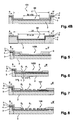
- FIGS. Figures 1 to 11 More specifically, the realization of the first level of conductive or semiconductive lines is illustrated in FIGS. Figures 1 to 11 .
- the method according to the invention comprises a first step 101 ( figure 1 ) of forming a first cavity 1, of rectangular shape, on a substrate 2, for example silicon.
- a deposit of a silicon oxide layer 3, of thickness 50 nm is produced on the substrate 2.
- the first cavity 1 a photolithography of the silicon oxide layer 3 is carried out. So, the bottom and the edges of the first cavity 1 are respectively formed by the substrate 2 and the silicon oxide layer 3.
- the deposition carried out during the first step 101 as well as the deposition carried out during the following steps can be carried out by methods known and controlled by those skilled in the art, such as the chemical deposition in vapor phase (CVD), sputter deposition, deposition by electron gun or deposition by thermal evaporation.
- CVD chemical deposition in vapor phase
- sputter deposition deposition by electron gun
- thermal evaporation deposition by thermal evaporation
- the width 11 of the first cavity 1 is determined so as to be compatible with a number of lines formed by a first polymer and a second polymer with a layer of a first diblock copolymer to be deposited. in a later step.
- each length of an element "x" is referenced by the designation Lx and each width of an element "x" is referenced by the designation Ix.
- a second step 102 ( figure 2 ) of the method according to the invention consists in making a deposit, on the bottom and on the edges of the first cavity 1, of a layer of an insulating material 4 of dielectric material, such as for example a silicon nitride.
- a third step 103 ( figure 3 ) of the method according to the invention consists in depositing, on the layer of the insulating material 4, a layer of a material 5 of silicon oxide.
- the latter preferentially comprises -OH type endings, having a chemical affinity for one of the phases of the copolymer which will be deposited thereafter.
- a fourth step 104 ( Figures 4A , 4B ) consists in forming a second cavity 6 of substantially rectangular shape and superimposed on the first cavity 1.
- the first and second cavities 1, 6 are moreover disposed substantially perpendicularly (ie the direction of the width of the one is perpendicular to the direction of the length of the other).
- a layer of a material 7 of silicon nitride is deposited over the entire surface of the layer 5 of silicon oxide material mentioned above.
- An engraving is then performed in the latter of in order to form the second cavity 6.
- a so-called dry etching method such as an O 2 plasma type etching or a so-called wet etching method of type H 3 PO 4 .
- the bottom of the second cavity 6 is formed by the layer of silicon oxide material 5 also forming the bottom and the edges of the first cavity 1. It may therefore be noted that the material 7 made of silicon nitride is selected so that it can be etched selectively with respect to the silicon oxide material.
- this second cavity 6 is superimposed on the first cavity 1 and the intersection of the first cavity 1 with the second cavity 6 forms a resultant cavity 8B whose bottom is formed by an intersection surface 8A (illustrated dotted on the Figure 4A ).
- the resulting cavity 8B has a length L8 formed by the width I1 of the first cavity 1 and a width 18 formed by the width I6 of the second cavity 6.
- the width I6 of the second cavity 6 is determined so as to be compatible with a number of lines formed by a third polymer and a fourth polymer of a layer of a second diblock copolymer which will be deposited in a subsequent step.
- a fifth step of the method according to the invention consists in covering the bottom of the resulting cavity 8B with a layer of a first diblock copolymer 9 comprising a network of lines formed by an alternation of lines of a first polymer P1 and lines a second polymer P2.
- the lines P1, P2 are arranged parallel along the length L6 of the second cavity 6.
- the thickness of this layer of first diblock copolymer 9 is preferably less than the depth of the first cavity 1.
- a perpendicular structure that is to say an orientation of the chains of the first and second polymers P1, P2 which is parallel to the substrate 2
- the interactions between the surface in contact (in species, the layer of material 5 of silicon oxide) and the different polymers P1 and P2 are different.
- the obtaining of a perpendicular structure is then obtained by neutralizing the surface in contact.
- the neutralization of a surface is conventionally obtained by means of a neutralization film (not shown) which may be a film of polymer material comprising randomly arranged polymer chains.
- the material layer 5 is made of silicon oxide
- a neutralization film of polymeric material comprising randomly arranged polymethyl methacrylate copolymer chains can be used.
- An exemplary embodiment is described by "Mansky et al. in Controlling Polymer-Surface Interactions with Random Copolymer Brushes »Science 275, 1458, 1997» .
- a copolymer with a structure perpendicular to the so-called lamellar substrate is conventionally obtained when the volume composition of the polymer chains is adapted.
- the composition The volume of one of the first or second polymers P1, P2 is preferably between 0.35 and 0.65.
- the recovery step can be carried out by depositing, on the bottom of the resulting cavity 8B, the layer of first diblock copolymer 9 comprising a network of pre-organized lines formed by an alternation of first polymer lines P1 and second polymer lines P2.
- a copolymer can be obtained by a thermal annealing method.
- first and second polymer lines P1, P2 are arranged parallel along the length L6 of the second cavity 6.
- the thickness of the layer of insulating material 4 deposited during the second step 102 may be of the order of the width of a first polymer line P1 added to the width of a second line.
- P2 polymer for example about 10 nm.
- a sixth step 105B ( figure 6 ) then makes it possible to structure the first diblock copolymer 9 in the resulting cavity 8B.
- the excess of the layer of the first diblock copolymer 9 which is disposed outside the resulting cavity 8B is suppressed.
- Such an action can be carried out, for example, by means of photolithography and etching or chemical mechanical polishing processes.
- the width 16 of the second cavity 6 is chosen so that it is equal to a multiple of the pitch of the first diblock copolymer 9, the pitch of the first diblock copolymer 9 being formed by the width ( or diameter) IP1 of a line (or chain) of first polymer P1 added to the width (or diameter) IP2 of a line (or a chain) of second polymer P2.
- This feature makes it possible to avoid constraining the layer of the first diblock copolymer 9 within the second cavity 6 and consequently within the resulting cavity 8B.
- the alternation of the first and second polymer lines P1, P2 preferably terminates at both ends of the resulting cavity 8B by a line of the same polymer (in our example the second polymer P2).
- the pitch of the network of a copolymer is controlled by the length of the polymer chains, while retaining the criterion relating to the composition of each of the polymers.
- a seventh step 107 ( figure 7 ) one of the phases of the layer of the first diblock copolymer 9 is removed so as to form alternating first grooves S1 and lines of second polymer P2.
- the layer of silicon oxide material 5 deposited during the third step 103 is then free at the location of the first grooves S1. If a neutralization film is used, it is also eliminated within these first bleeds.
- the elimination is carried out by any suitable technique.
- the first polymer P1 is polymethyl methacrylate
- An eighth step 108 ( figure 8 ) of the process according to the invention consists in removing, for example by SiO 2 etching CF4 plasma, said layer of silicon oxide material 5 forming the bottom of the first S1 bleeds. It follows that the bottom of the latter is formed by the layer of insulating material 4. This is made possible by the particularity of the material 5 which is selected so that it can be selectively etched. More particularly, the latter is chosen so as to be able to be etched selectively with respect to the second polymer P2 and to the insulating material 4.
- a ninth step 109 ( figure 9 ) of the method consists in producing a conformal deposition of a layer of a first conductive or semiconductor material 10, having a thickness substantially identical to that of the layer of silicon oxide material 5, at the bottom of the first grooves S1 and at the top of the second polymer lines P2.
- the first conductive or semiconductor material 10 is amorphous silicon, polycrystalline silicon or any other material having metallic or semiconductive properties. This material is deposited so as to at least partially fill the first grooves S1 and thus form first conductive or semiconducting lines 11 at the location of the lines of the first polymer P1 eliminated.
- a tenth step 110 ( Figure 10 and Figure 11 ) consists of removing, for example by etching, the second polymer lines P2.
- a lift-off type photolithography can be carried out making it possible to eliminate the second polymer lines P2 and the layer of the first conductive or semi-conductive material 10 located at the top of the second polymer lines P2.
- a plurality of first conductive or semiconducting lines 11 contained within the resulting cavity 8B are thus obtained. These first lines 11 are arranged on the layer of insulating material 4. More particularly, a plurality of first conductive or semiconductive lines 11 are obtained parallel to the length L6 of the second cavity 6 or to the length L8 of the resulting cavity. 8B.
- An eleventh step 111 ( figure 12 ) of the method consists in carrying out an etching of selective type, for example with a H 3 PO 4 based chemistry, so as to etch the layer of the material 7 forming the second cavity 6.
- the layer of material 7 filed during the fourth step 104 is eliminated.
- the material 7 has been chosen so that it can be etched selectively with respect to the silicon oxide material 5 and the first conductive or semiconductor material 10.
- a thirteenth step 113 ( figure 14 ) of the method consists in depositing a layer of a second conductive or semi-conducting material 14 on the layer of material 13 deposited during the twelfth step 112.
- a fourteenth stage 114 ( figure 15 ) is to perform a chemical modification of the surface of the layer of the second conductive or semi-conductive material 14 in order to increase the number of -OH terminations therein.
- This feature makes it possible to increase the affinity with the layer of second copolymer 16 which is deposited during the fifteenth following step.
- the number of -OH terminations may be increased by depositing, on the layer of the second conductive or semiconductor material 14, a layer of a HfO 2 type material whose free surface is rich in -OH termination. This material can be deposited by ALD (for Atomic Layer Deposition).
- a fifteenth step of the method according to the invention consists in covering the layer of material 15 or more generally the surface of the layer of the second conducting or semiconductor material 14 having been chemically modified with a layer of a second diblock copolymer 16 comprising a network of lines formed by an alternation of lines of a third polymer P3 and lines of a fourth polymer P4.
- the step of covering the material layer 15 can be carried out by depositing the second diblock copolymer 16 comprising a network of pre-organized lines formed by an alternation of third polymer lines. P3 and fourth polymer lines P4.
- the third and fourth polymer lines P3, P4 are arranged in parallel along the length L1 of the first cavity 1.
- the width 11 of the first cavity 1 is chosen so that it is equal to a multiple of the pitch of the second diblock copolymer 16, the pitch of the second diblock copolymer 16 being formed by the width (or diameter) IP3 of a line (or a chain) of third polymer P3 added to the IP4 width (or diameter) of a fourth polymer line (or chain) P4. This feature makes it possible to avoid constraining the layer of the second diblock copolymer 16 within the first cavity 1.
- the alternation of the third and fourth polymer lines P3, P4 ends preferably at the two ends of the first cavity 1 by a line of the same polymer (in our example the third polymer P3).
- third polymer P3 and fourth polymer P4 lines are substantially perpendicular to the first conductive or semi-conductive lines 11.
- a sixteenth step 115B makes it possible to structure the second diblock copolymer 16 in the first cavity 1.
- the excess of the layer of the second diblock copolymer 16 is eliminated. which is disposed outside the first cavity 1.
- Such an action can be performed, for example, by means of photolithography type processes and etching or chemical mechanical polishing.
- a seventeenth step 117 ( figure 18 ) consists in removing, for example by photolithography, one of the phases (the fourth polymer lines P4 in our example) of the second diblock copolymer layer 16 so as to form an alternation of second grooves S2 and third polymer lines P3.
- This step is performed in order to obtain an alternation of second conductive or semiconducting lines 17.
- the thickness of the copolymer does not make it possible to engrave the entire stack, it is possible to carry out a metal or Al 2 O 3 lift and to use the metal or Al 2 O 3 as a mask: after deposition of the second diblock copolymer 16, eliminates one phase with respect to the other, the metal or Al 2 O 3 is deposited by example by ALD (Atomic Layer Deposition) compliant, then it achieves a lift-off by plasma etching of the metal or Al 2 O 3 deposited on the copolymer phase that has not been removed; the remaining Al 2 O 3 or metal lines are used as the etching mask of the stack.
- ALD Atomic Layer Deposition
- the method furthermore comprises a nineteenth step 119 ( figure 20 ) during which the third polymer lines P3 are removed from the second copolymer layer 16. To do this, it is possible to perform a photolithography type etching.
- Such a grid 19 comprises a first level of lines 20 formed by the first conductive or semi-conductive lines 11 and a second level 21 of lines formed by the second conductive or semiconducting lines 17. More precisely, the grid 19 comprises on the layer of insulating material 4, in a plane parallel to the substrate 2, a first level of lines comprising a plurality of first lines 11 made in the first conductive or semiconductor material 10. In addition, on the first level of lines 11 there is a second level of lines 21 having a plurality of second lines 17 made in the second conductive or semiconductor material 14. The second lines 17 are substantially perpendicular to the first lines 11.
- the first and second cavities 1, 6 made respectively during the first step 101 and the fourth step 104 are made to micrometric dimensions.
- first and second diblock copolymers 9, 16 may, for example, each comprise a polymer of polymethyl methacrylate type and a polystyrene type polymer.
- the pitch of the first and second copolymers 9, 16 may be of the order of 20 nm.
- the layer of silicon oxide 3 deposited during the first step 101 for forming the first cavity 1 has a thickness of 50 nm or more so as to be greater than or equal to the sum of the thicknesses of the layer 13 possessing switching properties impedance by applying an electric field, the layer of the second conductive or semiconductor material 14, the layer of a material 15 whose free surface is rich in -OH termination and the layer of the second diblock copolymer 16,
- the cost and the time of realization of a grid 19 obtained by the implementation of the method of the invention is not dependent on the number of conductive or semiconducting lines produced.
Landscapes
- Semiconductor Memories (AREA)
- Bus Control (AREA)
Claims (12)
- Verfahren zum Ausführen eines Gitters (19) aus gekreuzten Leiter- oder Halbleiter-Anschlussleitungen auf einem Substrat (2), wobei das Gitter (19) Folgendes umfasst:- auf einem Gitterisolator (4) in einer zum Substrat (2) parallelen Ebene, eine erste Ebene (20) von Leitungen (11), die mehrere untereinander parallele erste Leitungen (11) umfasst, die in einem Leiter- oder Halbleitermaterial ausgeführt werden;- über der ersten Ebene (20) von Leitungen (11) eine zweite Ebene (21) von Leitungen (17), die mehrere untereinander parallele zweite Leitungen (17) umfasst, die in einem Leiter- oder Halbleitermaterial ausgeführt werden, wobei die zweiten Leitungen (17) im Wesentlichen senkrecht zu den ersten Leitungen (11) sind,wobei das Verfahren dadurch gekennzeichnet ist, dass es die folgenden Schritte umfasst:- Bilden (101) eines ersten Hohlraums (1) mit im Wesentlichen rechteckiger Form auf dem Substrat (2);- Bilden (104) eines zweiten Hohlraums (6) mit im Wesentlichen rechteckiger Form, der den ersten Hohlraum (1) überlagert, wobei der erste und der zweite Hohlraum (1, 6) sich derart senkrecht kreuzen, dass ein daraus resultierender Hohlraum (8B) gebildet wird;- Bedecken des Bodens des resultierenden Hohlraums (8B) mit einer Schicht aus einem ersten Diblockcopolymer (9) das ein Leitungsnetz umfasst, das durch einen Wechsel von Leitungen aus einem ersten Polymer (P1) und von Leitungen aus einem zweiten Polymer (P2) gebildet wird, wobei die Leitungen gemäß der Länge (L6) des zweiten Hohlraums (6) parallel angeordnet werden;- Entfernen (107) der Leitungen aus dem ersten Polymer (P1), derart, dass ein Wechsel von ersten Schnittfugen (S1) und von Leitungen aus dem zweiten Polymer (P2) gebildet wird;- Ausführen einer konformen Abscheidung (109) einer Schicht aus einem ersten Leiter- oder Halbleitermaterial (10) auf den Schnittfugen (S1) und den Leitungen aus dem zweiten Polymer (P2);- Entfernen (110) der Leitungen aus dem zweiten Polymer (P2), die mit dem ersten Leiter- oder Halbleitermaterial (10) bedeckt sind, derart, dass die erste Ebene (20) von Leitungen (11) ausgeführt wird;- selektives Entfernen (111) des Materials, das den zweiten Hohlraum (6) bildet, derart, dass der Boden des ersten Hohlraums (1), der gemäß seiner Breite (11) teilweise von der ersten Ebene (20) von Leitungen (11) bedeckt ist, zugänglich gemacht wird;- Abscheiden (113) einer Schicht aus einem zweiten Leiter- oder Halbleitermaterial (14) im ersten Hohlraum (1), der zugänglich gemacht wurde;- Bedecken der Schicht aus dem zweiten Leiter- oder Halbleitermaterial (14) mit einer Schicht aus einem zweiten Diblockcopolymer (16), die ein Leitungsnetz umfasst, das durch einen Wechsel von Leitungen aus einem dritten Polymer (P3) und von Leitungen aus einem vierten Polymer (P4) gebildet wird, wobei die Leitungen (P3, P4) im Wesentlichen senkrecht zu den ersten und zweiten Leitungen aus Polymeren (P1, P2) sind;- Entfernen (117) der Leitungen aus dem vierten Polymer (P4), derart, dass ein Wechsel von zweiten Schnittfugen (S2) und von Leitungen aus dem dritten Polymer (P3) gebildet wird;- Entfernen (118) des zweiten Leiter- oder Halbleitermaterials (14) in den zweiten Schnittfugen (S2), derart, dass die zweite Ebene (21) von Leitungen (17) ausgeführt wird.
- Verfahren nach dem vorhergehenden Anspruch, dadurch gekennzeichnet, dass es vor der Abscheidung (113) einer Schicht aus einem zweiten Leiter- oder Halbleitermaterial (14) in dem ersten Hohlraum (1), der zugänglich gemacht wurde, einen Schritt der Abscheidung (112) einer Schicht aus einem Material (13) umfasst, das Impedanzumschalteigenschaften durch Anlegen eines elektrischen Feldes umfasst, wobei der Schritt des Entfernens (118) in den zweiten Schnittfugen (S2) des zweiten Leiter- oder Halbleitermaterials (14) vom Entfernen der Materialschicht (13) begleitet wird, die Umschalteigenschaften umfasst.
- Verfahren nach dem vorhergehenden Anspruch, dadurch gekennzeichnet, dass das Material (13), das Impedanzumschalteigenschaften durch Anlegen eines elektrischen Feldes umfasst, vom folgenden Typ ist:- binäres Oxid;- Festelektrolyt;- Perowskit auf Basis von ternärem Oxid;- Phasenwechselmaterial;- Moleküle oder Polymere mit Widerstandsumschalteigenschaften; oder- magnetisches Material, das einen Tunnelübergang des magnetischen oder Spinventiltyps bilden kann.
- Verfahren nach einem der vorhergehenden Ansprüche, dadurch gekennzeichnet, dass:- der erste Hohlraum (1) eine Breite (11) aufweist, die gleich einem Vielfachen des Abstands des zweiten Diblockcopolymers (16) ist;- der zweite Hohlraum (1) eine Breite (16) aufweist, die gleich einem Vielfachen des Abstands des ersten Diblockcopolymers (9) ist.
- Verfahren nach einem der vorhergehenden Ansprüche, dadurch gekennzeichnet, dass dem Schritt der Bildung (101) des ersten Hohlraums (1) die zwei folgenden Schritte folgen:- Abscheiden (102) einer Schicht aus Isoliermaterial (4) auf den Rändern und dem Boden des ersten Hohlraums (1);- Abscheiden (103) einer Schicht aus einem Material (5), das geeignet ist, um auf selektive Weise in Bezug zu den Leitungen aus dem zweiten Polymer (P2) und dem Isoliermaterial (4) geätzt zu werden, auf der Schicht aus Isoliermaterial (4).
- Verfahren nach dem vorhergehenden Anspruch, dadurch gekennzeichnet, dass der Schritt der Bildung (104) des zweiten Hohlraums aus Folgendem besteht:- Abscheiden einer Schicht aus einem Material (7), das geeignet ist, um auf selektive Weise in Bezug auf das Material, das den Boden und die Ränder des ersten Hohlraums (1) bildet, geätzt zu werden;- Entfernen eines Abschnitts der Schicht aus dem Material (7), derart, dass der Boden des zweiten Hohlraums (6) durch den Boden des ersten Hohlraums (1) gebildet wird, der mit dem Material der Schicht aus dem Material (5) bedeckt ist, das geeignet ist, um auf selektive Weise in Bezug zu den Leitungen aus dem zweiten Polymer (P2) und dem Isoliermaterial (4) geätzt zu werden.
- Verfahren nach einem der Ansprüche 5 oder 6, dadurch gekennzeichnet, dass dem Schritt (107) der Entfernung der Leitungen aus dem ersten Polymer (P1) ein Schritt der Entfernung (108) des Materials (5), das geeignet ist, um auf selektive Weise in Bezug zu den Leitungen aus dem zweiten Polymer (P2) und zur Schicht aus Isoliermaterial (4) geätzt zu werden, durch erste Schnittfugen (S1) folgt.
- Verfahren nach einem der vorhergehenden Ansprüche, dadurch gekennzeichnet, dass der oder die Schritte des Bedeckens mit einem Diblockcopolymer durch die folgenden Schritte ausgeführt wird/werden:- Abscheiden (105A, 115A) der Diblockcopolymerschicht (9, 16);- Trennen (105B, 115B) der Phasen des abgeschiedenen Diblockcopolymers (9, 16), derart, dass ein Wechsel von Leitungen aus zwei verschiedenen Polymeren (P1, P2, P3, P4) ausgeführt wird.
- Verfahren nach einem der vorhergehenden Ansprüche, dadurch gekennzeichnet, dass jedem Schritt des Abdeckens mit einem Diblockcopolymer ein Strukturierungsschritt (105B, 115B) folgt, derart, dass das erste Diblockcopolymer (9) in dem resultierenden Hohlraum (8B) eingeschlossen wird und/oder das zweite Diblockcopolymer (16) in dem ersten Hohlraum (1) eingeschlossen wird.
- Verfahren nach einem der vorhergehenden Ansprüche, dadurch gekennzeichnet, dass vor dem Abscheiden des ersten und/oder zweiten Diblockcopolymers (9, 16) eine dünne Neutralisationsschicht abgeschieden wird.
- Verfahren nach einem der vorhergehenden Ansprüche, dadurch gekennzeichnet, dass dem Schritt des Abscheidens (113) des zweiten Leiter- oder Halbleitermaterials (14) ein Schritt der chemischen Veränderung (114) der Schicht aus dem zweiten Leiter- oder Halbleitermaterial (14) folgt, derart, dass Abschlüsse erhalten werden, die eine chemische Affinität für eine der Phasen des zweiten Diblockcopolymers (16) aufweisen.
- Verfahren nach einem der vorhergehenden Ansprüche, dadurch gekennzeichnet, dass:- eines des ersten oder zweiten Polymers (P1, P2) des ersten Diblockcopolymers (9) eine Volumenzusammensetzung aufweist, die zwischen 0,35 und 0,65 enthalten ist;- eines des dritten oder vierten Polymers (P3, P4) des zweiten Diblockcopolymers (16) eine Volumenzusammensetzung aufweist, die zwischen 0,35 und 0,65 enthalten ist.
Applications Claiming Priority (1)
| Application Number | Priority Date | Filing Date | Title |
|---|---|---|---|
| FR1054547A FR2961344B1 (fr) | 2010-06-09 | 2010-06-09 | Procede de realisation d?une grille de lignes conductrices ou semi-conductrices d?acces croisees |
Publications (2)
| Publication Number | Publication Date |
|---|---|
| EP2395543A1 EP2395543A1 (de) | 2011-12-14 |
| EP2395543B1 true EP2395543B1 (de) | 2013-01-16 |
Family
ID=43708744
Family Applications (1)
| Application Number | Title | Priority Date | Filing Date |
|---|---|---|---|
| EP11167959A Not-in-force EP2395543B1 (de) | 2010-06-09 | 2011-05-27 | Herstellungsverfahren eines Gitters aus überkreuzten Zugangsleiterbahnen |
Country Status (5)
| Country | Link |
|---|---|
| US (1) | US8685819B2 (de) |
| EP (1) | EP2395543B1 (de) |
| JP (1) | JP2012015497A (de) |
| CN (1) | CN102315172A (de) |
| FR (1) | FR2961344B1 (de) |
Families Citing this family (3)
| Publication number | Priority date | Publication date | Assignee | Title |
|---|---|---|---|---|
| KR101860250B1 (ko) * | 2014-02-23 | 2018-05-21 | 도쿄엘렉트론가부시키가이샤 | 반도체 기판들에서 콘택트들을 생성하기 위한 방법 |
| JP2016066644A (ja) | 2014-09-22 | 2016-04-28 | 株式会社東芝 | 記憶装置の製造方法 |
| FR3082033B1 (fr) * | 2018-06-05 | 2020-07-17 | Commissariat A L'energie Atomique Et Aux Energies Alternatives | Procede de fabrication d'un calculateur a reseaux de neurones recurrents |
Family Cites Families (4)
| Publication number | Priority date | Publication date | Assignee | Title |
|---|---|---|---|---|
| US4839700A (en) | 1987-12-16 | 1989-06-13 | California Institute Of Technology | Solid-state non-volatile electronically programmable reversible variable resistance device |
| EP1194960B1 (de) * | 1999-07-02 | 2010-09-15 | President and Fellows of Harvard College | Nanoskopischen draht enthaltende anordnung, logische felder und verfahren zu deren herstellung |
| US8207028B2 (en) * | 2008-01-22 | 2012-06-26 | International Business Machines Corporation | Two-dimensional patterning employing self-assembled material |
| WO2010082926A1 (en) * | 2009-01-14 | 2010-07-22 | Hewlett-Packard Development Company, L.P. | Method for doping an electrically actuated device |
-
2010
- 2010-06-09 FR FR1054547A patent/FR2961344B1/fr not_active Expired - Fee Related
-
2011
- 2011-05-27 EP EP11167959A patent/EP2395543B1/de not_active Not-in-force
- 2011-06-01 JP JP2011123367A patent/JP2012015497A/ja not_active Withdrawn
- 2011-06-07 US US13/154,726 patent/US8685819B2/en not_active Expired - Fee Related
- 2011-06-08 CN CN2011101599327A patent/CN102315172A/zh active Pending
Also Published As
| Publication number | Publication date |
|---|---|
| FR2961344A1 (fr) | 2011-12-16 |
| EP2395543A1 (de) | 2011-12-14 |
| JP2012015497A (ja) | 2012-01-19 |
| US8685819B2 (en) | 2014-04-01 |
| US20120052598A1 (en) | 2012-03-01 |
| CN102315172A (zh) | 2012-01-11 |
| FR2961344B1 (fr) | 2012-07-13 |
Similar Documents
| Publication | Publication Date | Title |
|---|---|---|
| US7034332B2 (en) | Nanometer-scale memory device utilizing self-aligned rectifying elements and method of making | |
| EP2453470B1 (de) | Verfahren zum Formen einer Mehrschichtenstruktur | |
| EP3012880B1 (de) | Nicht-flüchtige hybrid-speichervorrichtung, und herstellungsverfahren einer solchen vorrichtung | |
| EP2998981B1 (de) | Grapho-epitaxie-verfahren zur umsetzung von motiven auf der oberfläche eines substrats | |
| KR102047140B1 (ko) | 블록-공중합체를 이용하는 에칭 방법 | |
| TW201023271A (en) | Methods of forming diodes | |
| US7750386B2 (en) | Memory cells including nanoporous layers containing conductive material | |
| FR2945891A1 (fr) | Structure semiconductrice et procede de realisation d'une structure semiconductrice. | |
| EP2681776A2 (de) | Verfahren zur metallisierung von strukturierten oberflächen | |
| EP3503165A1 (de) | Verfahren zur bildung einer chemischen leitstruktur auf einem substrat, und chemo-epitaxie-verfahren | |
| EP2395543B1 (de) | Herstellungsverfahren eines Gitters aus überkreuzten Zugangsleiterbahnen | |
| FR3057991B1 (fr) | Procede de formation d’un guide d’assemblage fonctionnalise | |
| FR2895531A1 (fr) | Procede ameliore de realisation de cellules memoires de type pmc | |
| EP2487708B1 (de) | Verfahren zum Erstellen eines Netzes aus nanometrischen Kontakten | |
| CN110993565A (zh) | 一种定向自组装制备半导体纳米器件结构的方法 | |
| WO2019122334A1 (fr) | Procédé de formation d'une structure de guidage chimique sur un substrat et procédé de chémo-épitaxie | |
| FR3009430A1 (fr) | Procede de realisation d'un motif dans un circuit integre et circuit integre correspondant | |
| Meier et al. | A multilayer RRAM nanoarchitecture with resistively switching Ag-doped spin-on glass | |
| FR2927467A1 (fr) | Procede de realisation d'une grille flottante ayant une alternance de lignes en premier et second materiaux | |
| FR3071646B1 (fr) | Procede de fabrication d'un calculateur a reseaux de neurones recurrents | |
| FR3113409A1 (fr) | Procede de realisation d’un dispositif quantique a qubits de spin nucleaire | |
| JP4660306B2 (ja) | 集積回路装置の製造方法 | |
| EP4661066A1 (de) | Durchkontaktierungsstruktur durch metallebenen | |
| KR101089396B1 (ko) | 3차원 임프린트 및 리프트 오프 공정을 이용한 교차형 상변환 소자 제조 방법 및 그 방법에 의해 제조된 교차형 상변환 소자 | |
| EP2226679B1 (de) | Verfahren zur Herstellung einer Nanoimprintform |
Legal Events
| Date | Code | Title | Description |
|---|---|---|---|
| AK | Designated contracting states |
Kind code of ref document: A1 Designated state(s): AL AT BE BG CH CY CZ DE DK EE ES FI FR GB GR HR HU IE IS IT LI LT LU LV MC MK MT NL NO PL PT RO RS SE SI SK SM TR |
|
| AX | Request for extension of the european patent |
Extension state: BA ME |
|
| PUAI | Public reference made under article 153(3) epc to a published international application that has entered the european phase |
Free format text: ORIGINAL CODE: 0009012 |
|
| 17P | Request for examination filed |
Effective date: 20120519 |
|
| GRAP | Despatch of communication of intention to grant a patent |
Free format text: ORIGINAL CODE: EPIDOSNIGR1 |
|
| RIC1 | Information provided on ipc code assigned before grant |
Ipc: G03F 7/033 20060101ALI20120719BHEP Ipc: H01L 21/3213 20060101ALI20120719BHEP Ipc: H01L 21/033 20060101AFI20120719BHEP |
|
| GRAS | Grant fee paid |
Free format text: ORIGINAL CODE: EPIDOSNIGR3 |
|
| GRAA | (expected) grant |
Free format text: ORIGINAL CODE: 0009210 |
|
| AK | Designated contracting states |
Kind code of ref document: B1 Designated state(s): AL AT BE BG CH CY CZ DE DK EE ES FI FR GB GR HR HU IE IS IT LI LT LU LV MC MK MT NL NO PL PT RO RS SE SI SK SM TR |
|
| REG | Reference to a national code |
Ref country code: GB Ref legal event code: FG4D Free format text: NOT ENGLISH |
|
| REG | Reference to a national code |
Ref country code: CH Ref legal event code: EP |
|
| REG | Reference to a national code |
Ref country code: IE Ref legal event code: FG4D Free format text: LANGUAGE OF EP DOCUMENT: FRENCH |
|
| REG | Reference to a national code |
Ref country code: AT Ref legal event code: REF Ref document number: 594286 Country of ref document: AT Kind code of ref document: T Effective date: 20130215 Ref country code: CH Ref legal event code: EP |
|
| REG | Reference to a national code |
Ref country code: DE Ref legal event code: R096 Ref document number: 602011000776 Country of ref document: DE Effective date: 20130314 |
|
| REG | Reference to a national code |
Ref country code: AT Ref legal event code: MK05 Ref document number: 594286 Country of ref document: AT Kind code of ref document: T Effective date: 20130116 |
|
| REG | Reference to a national code |
Ref country code: NL Ref legal event code: VDEP Effective date: 20130116 |
|
| REG | Reference to a national code |
Ref country code: LT Ref legal event code: MG4D |
|
| PG25 | Lapsed in a contracting state [announced via postgrant information from national office to epo] |
Ref country code: SE Free format text: LAPSE BECAUSE OF FAILURE TO SUBMIT A TRANSLATION OF THE DESCRIPTION OR TO PAY THE FEE WITHIN THE PRESCRIBED TIME-LIMIT Effective date: 20130116 Ref country code: NO Free format text: LAPSE BECAUSE OF FAILURE TO SUBMIT A TRANSLATION OF THE DESCRIPTION OR TO PAY THE FEE WITHIN THE PRESCRIBED TIME-LIMIT Effective date: 20130416 Ref country code: LT Free format text: LAPSE BECAUSE OF FAILURE TO SUBMIT A TRANSLATION OF THE DESCRIPTION OR TO PAY THE FEE WITHIN THE PRESCRIBED TIME-LIMIT Effective date: 20130116 Ref country code: BG Free format text: LAPSE BECAUSE OF FAILURE TO SUBMIT A TRANSLATION OF THE DESCRIPTION OR TO PAY THE FEE WITHIN THE PRESCRIBED TIME-LIMIT Effective date: 20130416 Ref country code: IS Free format text: LAPSE BECAUSE OF FAILURE TO SUBMIT A TRANSLATION OF THE DESCRIPTION OR TO PAY THE FEE WITHIN THE PRESCRIBED TIME-LIMIT Effective date: 20130516 Ref country code: ES Free format text: LAPSE BECAUSE OF FAILURE TO SUBMIT A TRANSLATION OF THE DESCRIPTION OR TO PAY THE FEE WITHIN THE PRESCRIBED TIME-LIMIT Effective date: 20130427 Ref country code: AT Free format text: LAPSE BECAUSE OF FAILURE TO SUBMIT A TRANSLATION OF THE DESCRIPTION OR TO PAY THE FEE WITHIN THE PRESCRIBED TIME-LIMIT Effective date: 20130116 |
|
| PG25 | Lapsed in a contracting state [announced via postgrant information from national office to epo] |
Ref country code: PL Free format text: LAPSE BECAUSE OF FAILURE TO SUBMIT A TRANSLATION OF THE DESCRIPTION OR TO PAY THE FEE WITHIN THE PRESCRIBED TIME-LIMIT Effective date: 20130116 Ref country code: GR Free format text: LAPSE BECAUSE OF FAILURE TO SUBMIT A TRANSLATION OF THE DESCRIPTION OR TO PAY THE FEE WITHIN THE PRESCRIBED TIME-LIMIT Effective date: 20130417 Ref country code: SI Free format text: LAPSE BECAUSE OF FAILURE TO SUBMIT A TRANSLATION OF THE DESCRIPTION OR TO PAY THE FEE WITHIN THE PRESCRIBED TIME-LIMIT Effective date: 20130116 Ref country code: FI Free format text: LAPSE BECAUSE OF FAILURE TO SUBMIT A TRANSLATION OF THE DESCRIPTION OR TO PAY THE FEE WITHIN THE PRESCRIBED TIME-LIMIT Effective date: 20130116 Ref country code: LV Free format text: LAPSE BECAUSE OF FAILURE TO SUBMIT A TRANSLATION OF THE DESCRIPTION OR TO PAY THE FEE WITHIN THE PRESCRIBED TIME-LIMIT Effective date: 20130116 Ref country code: PT Free format text: LAPSE BECAUSE OF FAILURE TO SUBMIT A TRANSLATION OF THE DESCRIPTION OR TO PAY THE FEE WITHIN THE PRESCRIBED TIME-LIMIT Effective date: 20130516 Ref country code: NL Free format text: LAPSE BECAUSE OF FAILURE TO SUBMIT A TRANSLATION OF THE DESCRIPTION OR TO PAY THE FEE WITHIN THE PRESCRIBED TIME-LIMIT Effective date: 20130116 |
|
| PG25 | Lapsed in a contracting state [announced via postgrant information from national office to epo] |
Ref country code: HR Free format text: LAPSE BECAUSE OF FAILURE TO SUBMIT A TRANSLATION OF THE DESCRIPTION OR TO PAY THE FEE WITHIN THE PRESCRIBED TIME-LIMIT Effective date: 20130116 Ref country code: RS Free format text: LAPSE BECAUSE OF FAILURE TO SUBMIT A TRANSLATION OF THE DESCRIPTION OR TO PAY THE FEE WITHIN THE PRESCRIBED TIME-LIMIT Effective date: 20130116 |
|
| PG25 | Lapsed in a contracting state [announced via postgrant information from national office to epo] |
Ref country code: CZ Free format text: LAPSE BECAUSE OF FAILURE TO SUBMIT A TRANSLATION OF THE DESCRIPTION OR TO PAY THE FEE WITHIN THE PRESCRIBED TIME-LIMIT Effective date: 20130116 Ref country code: SK Free format text: LAPSE BECAUSE OF FAILURE TO SUBMIT A TRANSLATION OF THE DESCRIPTION OR TO PAY THE FEE WITHIN THE PRESCRIBED TIME-LIMIT Effective date: 20130116 Ref country code: RO Free format text: LAPSE BECAUSE OF FAILURE TO SUBMIT A TRANSLATION OF THE DESCRIPTION OR TO PAY THE FEE WITHIN THE PRESCRIBED TIME-LIMIT Effective date: 20130116 Ref country code: EE Free format text: LAPSE BECAUSE OF FAILURE TO SUBMIT A TRANSLATION OF THE DESCRIPTION OR TO PAY THE FEE WITHIN THE PRESCRIBED TIME-LIMIT Effective date: 20130116 Ref country code: DK Free format text: LAPSE BECAUSE OF FAILURE TO SUBMIT A TRANSLATION OF THE DESCRIPTION OR TO PAY THE FEE WITHIN THE PRESCRIBED TIME-LIMIT Effective date: 20130116 |
|
| PLBE | No opposition filed within time limit |
Free format text: ORIGINAL CODE: 0009261 |
|
| STAA | Information on the status of an ep patent application or granted ep patent |
Free format text: STATUS: NO OPPOSITION FILED WITHIN TIME LIMIT |
|
| PG25 | Lapsed in a contracting state [announced via postgrant information from national office to epo] |
Ref country code: CY Free format text: LAPSE BECAUSE OF FAILURE TO SUBMIT A TRANSLATION OF THE DESCRIPTION OR TO PAY THE FEE WITHIN THE PRESCRIBED TIME-LIMIT Effective date: 20130116 |
|
| BERE | Be: lapsed |
Owner name: COMMISSARIAT A L'ENERGIE ATOMIQUE ET AUX ENERGIES Effective date: 20130531 Owner name: CENTRE NATIONAL DE LA RECHERCHE SCIENTIFIQUE Effective date: 20130531 Owner name: UNIVERSITE JOSEPH FOURIER Effective date: 20130531 |
|
| 26N | No opposition filed |
Effective date: 20131017 |
|
| PG25 | Lapsed in a contracting state [announced via postgrant information from national office to epo] |
Ref country code: IT Free format text: LAPSE BECAUSE OF FAILURE TO SUBMIT A TRANSLATION OF THE DESCRIPTION OR TO PAY THE FEE WITHIN THE PRESCRIBED TIME-LIMIT Effective date: 20130116 Ref country code: MC Free format text: LAPSE BECAUSE OF FAILURE TO SUBMIT A TRANSLATION OF THE DESCRIPTION OR TO PAY THE FEE WITHIN THE PRESCRIBED TIME-LIMIT Effective date: 20130116 |
|
| REG | Reference to a national code |
Ref country code: DE Ref legal event code: R097 Ref document number: 602011000776 Country of ref document: DE Effective date: 20131017 |
|
| REG | Reference to a national code |
Ref country code: IE Ref legal event code: MM4A |
|
| PG25 | Lapsed in a contracting state [announced via postgrant information from national office to epo] |
Ref country code: BE Free format text: LAPSE BECAUSE OF NON-PAYMENT OF DUE FEES Effective date: 20130531 |
|
| PG25 | Lapsed in a contracting state [announced via postgrant information from national office to epo] |
Ref country code: IE Free format text: LAPSE BECAUSE OF NON-PAYMENT OF DUE FEES Effective date: 20130527 |
|
| REG | Reference to a national code |
Ref country code: CH Ref legal event code: PL |
|
| PG25 | Lapsed in a contracting state [announced via postgrant information from national office to epo] |
Ref country code: LI Free format text: LAPSE BECAUSE OF NON-PAYMENT OF DUE FEES Effective date: 20140531 Ref country code: CH Free format text: LAPSE BECAUSE OF NON-PAYMENT OF DUE FEES Effective date: 20140531 |
|
| PG25 | Lapsed in a contracting state [announced via postgrant information from national office to epo] |
Ref country code: MT Free format text: LAPSE BECAUSE OF FAILURE TO SUBMIT A TRANSLATION OF THE DESCRIPTION OR TO PAY THE FEE WITHIN THE PRESCRIBED TIME-LIMIT Effective date: 20130116 |
|
| PG25 | Lapsed in a contracting state [announced via postgrant information from national office to epo] |
Ref country code: SM Free format text: LAPSE BECAUSE OF FAILURE TO SUBMIT A TRANSLATION OF THE DESCRIPTION OR TO PAY THE FEE WITHIN THE PRESCRIBED TIME-LIMIT Effective date: 20130116 |
|
| PG25 | Lapsed in a contracting state [announced via postgrant information from national office to epo] |
Ref country code: TR Free format text: LAPSE BECAUSE OF FAILURE TO SUBMIT A TRANSLATION OF THE DESCRIPTION OR TO PAY THE FEE WITHIN THE PRESCRIBED TIME-LIMIT Effective date: 20130116 |
|
| PG25 | Lapsed in a contracting state [announced via postgrant information from national office to epo] |
Ref country code: LU Free format text: LAPSE BECAUSE OF NON-PAYMENT OF DUE FEES Effective date: 20130527 Ref country code: HU Free format text: LAPSE BECAUSE OF FAILURE TO SUBMIT A TRANSLATION OF THE DESCRIPTION OR TO PAY THE FEE WITHIN THE PRESCRIBED TIME-LIMIT; INVALID AB INITIO Effective date: 20110527 Ref country code: MK Free format text: LAPSE BECAUSE OF FAILURE TO SUBMIT A TRANSLATION OF THE DESCRIPTION OR TO PAY THE FEE WITHIN THE PRESCRIBED TIME-LIMIT Effective date: 20130116 |
|
| PGFP | Annual fee paid to national office [announced via postgrant information from national office to epo] |
Ref country code: GB Payment date: 20150424 Year of fee payment: 5 |
|
| REG | Reference to a national code |
Ref country code: FR Ref legal event code: PLFP Year of fee payment: 6 |
|
| REG | Reference to a national code |
Ref country code: DE Ref legal event code: R081 Ref document number: 602011000776 Country of ref document: DE Owner name: COMMISSARIAT A L'ENERGIE ATOMIQUE ET AUX ENERG, FR Free format text: FORMER OWNERS: CENTRE NATIONAL DE LA RECHERCHE SCIENTIFIQUE, PARIS, FR; COMMISSARIAT A L'ENERGIE ATOMIQUE ET AUX ENERGIES ALTERNATIVES, PARIS, FR; UNIVERSITE JOSEPH FOURIER, GRENOBLE, FR Ref country code: DE Ref legal event code: R082 Ref document number: 602011000776 Country of ref document: DE Representative=s name: CABINET CAMUS LEBKIRI, FR |
|
| REG | Reference to a national code |
Ref country code: FR Ref legal event code: CD Owner name: LE COMMISSARIAT A L'ENERGIE ATOMIQUE ET AUX EN, FR Effective date: 20160705 Ref country code: FR Ref legal event code: TP Owner name: LE COMMISSARIAT A L'ENERGIE ATOMIQUE ET AUX EN, FR Effective date: 20160705 Ref country code: FR Ref legal event code: CA Effective date: 20160705 |
|
| GBPC | Gb: european patent ceased through non-payment of renewal fee |
Effective date: 20160527 |
|
| REG | Reference to a national code |
Ref country code: FR Ref legal event code: PLFP Year of fee payment: 7 |
|
| PG25 | Lapsed in a contracting state [announced via postgrant information from national office to epo] |
Ref country code: GB Free format text: LAPSE BECAUSE OF NON-PAYMENT OF DUE FEES Effective date: 20160527 |
|
| PGFP | Annual fee paid to national office [announced via postgrant information from national office to epo] |
Ref country code: DE Payment date: 20170420 Year of fee payment: 7 Ref country code: FR Payment date: 20170421 Year of fee payment: 7 |
|
| PG25 | Lapsed in a contracting state [announced via postgrant information from national office to epo] |
Ref country code: AL Free format text: LAPSE BECAUSE OF FAILURE TO SUBMIT A TRANSLATION OF THE DESCRIPTION OR TO PAY THE FEE WITHIN THE PRESCRIBED TIME-LIMIT Effective date: 20130116 |
|
| REG | Reference to a national code |
Ref country code: DE Ref legal event code: R119 Ref document number: 602011000776 Country of ref document: DE |
|
| PG25 | Lapsed in a contracting state [announced via postgrant information from national office to epo] |
Ref country code: FR Free format text: LAPSE BECAUSE OF NON-PAYMENT OF DUE FEES Effective date: 20180531 Ref country code: DE Free format text: LAPSE BECAUSE OF NON-PAYMENT OF DUE FEES Effective date: 20181201 |