EP2391024A1 - Filtern von erkannten Störungen in einem drahtlosen Empfänger - Google Patents
Filtern von erkannten Störungen in einem drahtlosen Empfänger Download PDFInfo
- Publication number
- EP2391024A1 EP2391024A1 EP10164466A EP10164466A EP2391024A1 EP 2391024 A1 EP2391024 A1 EP 2391024A1 EP 10164466 A EP10164466 A EP 10164466A EP 10164466 A EP10164466 A EP 10164466A EP 2391024 A1 EP2391024 A1 EP 2391024A1
- Authority
- EP
- European Patent Office
- Prior art keywords
- interference
- filter
- different
- digital
- analog
- Prior art date
- Legal status (The legal status is an assumption and is not a legal conclusion. Google has not performed a legal analysis and makes no representation as to the accuracy of the status listed.)
- Granted
Links
- 238000001914 filtration Methods 0.000 title claims abstract description 18
- 238000000034 method Methods 0.000 claims description 33
- 230000005540 biological transmission Effects 0.000 claims description 5
- 238000004590 computer program Methods 0.000 claims description 5
- 230000008901 benefit Effects 0.000 abstract description 5
- 230000001629 suppression Effects 0.000 description 19
- 238000001514 detection method Methods 0.000 description 12
- 230000000694 effects Effects 0.000 description 11
- 238000012545 processing Methods 0.000 description 11
- 238000001228 spectrum Methods 0.000 description 7
- 238000005070 sampling Methods 0.000 description 5
- 238000013459 approach Methods 0.000 description 4
- 238000006243 chemical reaction Methods 0.000 description 4
- 238000013461 design Methods 0.000 description 4
- 230000003449 preventive effect Effects 0.000 description 4
- 230000006870 function Effects 0.000 description 3
- 230000008569 process Effects 0.000 description 3
- 239000007787 solid Substances 0.000 description 3
- 230000006399 behavior Effects 0.000 description 2
- 239000000969 carrier Substances 0.000 description 2
- 230000002452 interceptive effect Effects 0.000 description 2
- 230000007246 mechanism Effects 0.000 description 2
- 230000003287 optical effect Effects 0.000 description 2
- 238000013139 quantization Methods 0.000 description 2
- 230000000246 remedial effect Effects 0.000 description 2
- 238000010183 spectrum analysis Methods 0.000 description 2
- XUIMIQQOPSSXEZ-UHFFFAOYSA-N Silicon Chemical compound [Si] XUIMIQQOPSSXEZ-UHFFFAOYSA-N 0.000 description 1
- 230000003213 activating effect Effects 0.000 description 1
- 230000003044 adaptive effect Effects 0.000 description 1
- 230000004931 aggregating effect Effects 0.000 description 1
- 230000002776 aggregation Effects 0.000 description 1
- 238000004220 aggregation Methods 0.000 description 1
- 238000004458 analytical method Methods 0.000 description 1
- 239000000872 buffer Substances 0.000 description 1
- 238000012512 characterization method Methods 0.000 description 1
- 230000001149 cognitive effect Effects 0.000 description 1
- 238000004891 communication Methods 0.000 description 1
- 230000001419 dependent effect Effects 0.000 description 1
- 238000005516 engineering process Methods 0.000 description 1
- 230000010365 information processing Effects 0.000 description 1
- 230000010354 integration Effects 0.000 description 1
- 238000012804 iterative process Methods 0.000 description 1
- 238000005259 measurement Methods 0.000 description 1
- 230000000116 mitigating effect Effects 0.000 description 1
- 238000012986 modification Methods 0.000 description 1
- 230000004048 modification Effects 0.000 description 1
- 229910052710 silicon Inorganic materials 0.000 description 1
- 239000010703 silicon Substances 0.000 description 1
- 230000003595 spectral effect Effects 0.000 description 1
- 238000012546 transfer Methods 0.000 description 1
- 230000007704 transition Effects 0.000 description 1
Images


Classifications
-
- H—ELECTRICITY
- H04—ELECTRIC COMMUNICATION TECHNIQUE
- H04B—TRANSMISSION
- H04B1/00—Details of transmission systems, not covered by a single one of groups H04B3/00 - H04B13/00; Details of transmission systems not characterised by the medium used for transmission
- H04B1/06—Receivers
- H04B1/10—Means associated with receiver for limiting or suppressing noise or interference
- H04B1/1027—Means associated with receiver for limiting or suppressing noise or interference assessing signal quality or detecting noise/interference for the received signal
- H04B1/1036—Means associated with receiver for limiting or suppressing noise or interference assessing signal quality or detecting noise/interference for the received signal with automatic suppression of narrow band noise or interference, e.g. by using tuneable notch filters
Definitions
- This invention relates to methods of operating a wireless receiver. It also relates to corresponding wireless receivers, and to equipment incorporating such wireless receivers, and to programs for controlling such wireless receivers.
- W02009114123A2 It is known from W02009114123A2 to have a wideband signal processing apparatus for software defined radio that can include a transceiver configured to receive a UWB signal via an antenna.
- a spectrum analyzer provides a characterization of the UWB signal, which may be used to set a reconfigurable band-reject filter (BRF) to null detected interferers. Changing a gain of the band-reject filter adjusts a centre frequency of the band-reject filter.
- BRF reconfigurable band-reject filter
- An object of the invention is to provide improved apparatus or methods. According to a first aspect, the invention provides:
- the filtering can be better matched to the detected interference, or the drawbacks can be reduced for example.
- Embodiments of the invention can have any other features added, and some such additional features are set out in dependent claims and described in more detail below.
- a wireless receiver for receiving a useful signal in a particular band of frequencies in spite of interference, the receiver having two or more different types of tunable band reject filter, and an interference detector for detecting interference in the received signal.
- circuitry arranged to select which of the different types of filter to use according to different thresholds of the parameters of the detected interference, and circuitry for tuning the selected filter or filters according to the detected interference to filter the interference.
- Another aspect of the present invention is a computer program product comprising instructions which when executed by the computer cause the computer to carry out a method of controlling a wireless receiver to receive a signal, the wireless receiver comprising tunable band reject filters of at least two different types, the method comprising the steps of:
- Elements or parts of the described receivers may comprise logic encoded in media for performing any kind of information processing.
- Logic may comprise software encoded in a disk or other computer-readable medium and/or instructions encoded in an application specific integrated circuit (ASIC), field programmable gate array (FPGA), or other processor or hardware.
- ASIC application specific integrated circuit
- FPGA field programmable gate array
- references to software can encompass any type of programs in any language executable directly or indirectly by a processor.
- references to logic, hardware, processor or circuitry can encompass any kind of logic or analog circuitry, integrated to any degree, and not limited to general purpose processors, digital signal processors, ASICs, FPGAs, discrete components or transistor logic gates and so on.
- References to interference can encompass any type of interference, narrow band or broadband, continuing or intermittent, or to any part of the interference.
- References to receiving are intended to encompass downshifting frequencies to baseband, or distinguishing a band of frequencies, according to the context.
- Embodiments to be described can be applied in for example Narrowband interference (NBI) mitigation, OFDM, Wimedia based UWB, Wireless USB, media-access-control (MAC), Cognitive radio, and so on.
- NBI Narrowband interference
- the output of the detection can be used to tune a BRF such as a notch filter, to cancel the affect of the NBI.
- the FCC and ITU-R define UWB in terms of a transmission from an antenna for which the emitted signal bandwidth exceeds the lesser of 500 MHz or 20% of the centre frequency.
- each transmitted pulse instantaneously occupies the UWB bandwidth, or an aggregation of at least 500 MHz worth of narrow band carriers, for example in orthogonal frequency-division multiplexing (OFDM) fashion-can gain access to the UWB spectrum.
- OFDM orthogonal frequency-division multiplexing
- Unlicensed use of UWB can be in the range of 3.1 to 10.6 GHz.
- the useful signal information can be modulated on UWB pulses by encoding the polarity of the pulse, the amplitude of the pulse, and/or by using orthogonal pulses.
- UWB pulses can be sent sporadically at relatively low pulse rates to support time/position modulation, but can also be sent at rates up to the inverse of the UWB pulse bandwidth.
- UWB systems tend to be short-range and indoors applications. However, due to the short duration of the UWB pulses, it is easier to engineer extremely high data rates, and data rate can be readily traded for range by simply aggregating pulse energy per data bit using either simple integration or by coding techniques. Conventional OFDM (Orthogonal Frequency Division Multiplexing) technology can also be used.
- OFDM Orthogonal Frequency Division Multiplexing
- the known solutions adopt a two step approach and involve the suppression of the unwanted interferences by using band reject filters (BRF).
- BRF band reject filters
- This approach uses FFT as a rough spectrometer to analyze the spectrum of incoming signal for interference detection.
- the input sampling rate of FFT blocks is corresponding to the bandwidth of the system.
- the ADC uses a higher sampling rate to ease the requirements of analog baseband filtering and is generally followed by a downsampler so that the rest of digital baseband functions at a lower sampling rate. Therefore, the sampling rate at an FFT block is lower than the sampling rate of the ADC.
- the FFT performs the spectrum analysis on the frequency band corresponding to bandwidth of the UWB signal (528 MHz). Therefore, the current solutions have a search space which covers the in-band interferences.
- the ADC output is first downsampled before further baseband processing.
- a power detector is placed just after the ADC, and measures the power of incoming samples. This measurement is used as an input to a gain control part (AGC). This ensures that the analog input signal fits into the maximum signal range supported by the ADC and hence, does not suffer from clipping at ADC.
- AGC gain control part
- a digital BRF scheme can simplify the cost of an analog-BR-only interference suppression solution for example.
- an adaptive mechanism is proposed to select which of the different types (analog and or digital for example) of BRFs to use, based on the amount of interference from other systems. This can help limit the negative side-effects of a fixed analog-only solution, or a solution in which digital filtering is not selected and controlled independently.
- this independent selection can enable tuning to different frequencies to suppress multiple interferers instead of a single interferer only.
- Some embodiments can be simplified in terms of area and power consumption if the filtering performance requirements of the analog BRF can be relaxed.
- An analog BRF also causes certain negative side effects such as ringing, group delay, longer settling time etc. These effects are in proportion to the order of the BRF. So, it can be better to reduce the filter-order of analog BRF as much as possible.
- digital assistance for analog BRFs can be adapted to be selected independently, to combat narrowband interference (NBI) more effectively.
- the digital assistance can be provided by using an additional digital BRF and/or tone-nulling in the frequency domain. This can not only make the system more efficient with respect to the analog BRF, but also provides more flexibility in overall system behavior.
- a wireless receiver 110 can receive transmissions from a transmitter (not shown).
- the receiver has receiver circuitry 120, to derive a useful signal in a particular band of frequencies in spite of interference components inside and outside the particular band of frequencies.
- An interference detector 130 is provided which can detect in band interference at least.
- the receiver circuitry includes at least two different types of band rejection filter, 121 and 122, shown as types A and B respectively, which can be analog or digital.
- Circuitry 134 is provided to compare a parameter of the interference to different thresholds to select which of the types of BRF to use. This can operate based on the power and/or other characteristics of the detected interference, or the number of interferers detected at different frequencies for example.
- Circuitry 137 is also provided to selecte the BRF or BRFs according to the different thresholds to suppress the detected interference, implementable either as separate circuits or integrated together.
- the selected BRFs can then be tuned to the detected interference by tuning control circuit 138, to tune at least the frequency (as detected by the interference detector) and in some cases the bandwidth or attenuation level.
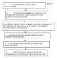
- step 15 steps in operating a wireless receiver such as that of figure 1 , or other embodiments are shown.
- a signal is received, having the useful signal in a particular band.
- the receiver circuitry operates to receive (meaning distinguish) the particular band, and the interference detector detects the interference. Such detection can be carried out in various ways, as will be described in more detail below.
- step 25 a comparison is made to different thresholds to enable the selection between the different types of BRFs, to provide a more appropriate or efficient match of the BRF to the interference.
- the selection can involve adjusting the proportion of the suppression by the different types, as well as switching only one of them into use, without the other, to optimise the suppression or minimise the drawbacks of the different types.
- the selected BRF or BRFs is or are tuned to suppress the detected interference. This can of course be an iterative process, to achieve the best suppression, by adjusting the amount or frequencies of the suppression and detecting the remaining interference for example.
- the interference can be distinguished from the useful signal in various ways, depending on how the useful signal is coded or spread over the bandwidth of the channel.
- the useful signal is received by the receiver circuitry with the interference suppressed using the selected BRF or BRFs.
- Figure 3 shows parts of a receiver according to an embodiment having type A in the form of an analog tunable BRF 505 and type B in the form of a digital tunable BRF 590.
- the receiver circuitry has an analog front end 505 which feeds the tunable analog BRF.
- An AD converter 340 converts the filtered analog signal into a digital signal. This is fed to the digital BRF 590, and the filtered output of the digital BRF is fed to other digital functions 247.
- the interference detector is shown with inputs from the analog or digital signal, to show that in principle it can be coupled at various locations and implemented in analog or digital form, though a digital form is almost always more practical.
- the tunable analog and digital BRFs are controlled by circuitry 237 for comparing the interference with different thresholds, and circuitry 239 for selecting and tuning, based on the different thresholds, as discussed above.
- circuitry 237 for comparing the interference with different thresholds
- circuitry 239 for selecting and tuning, based on the different thresholds, as discussed above.
- Other parts not shown can be added in between or after the parts shown.
- FIG. 4 There are various ways of operating the embodiment of figure 3 to benefit from the separate selection of the types of BRF.
- One way is shown in figure 4 .
- the signal is received at step 15 and the interference is detected, without filtering initially.
- the strength of the interference is compared to a first threshold for using the digital filter only without the analog filter.
- Step 33 involves selecting both filters if the interference is above that first threshold. If below, a second lower threshold is used, and the digital filter only is selected if the interference is between thresholds according to the result of that comparison to provide a more appropriate or efficient match of the BRF to the interference.
- the selection can involve adjusting the proportion of the suppression by the different types, as well as switching only one of them into use, without the other, to optimise the suppression or minimise the drawbacks of the different types.
- the interference is below the lower threshold, at step 43, neither of the BRFs is selected.
- the selected BRF or BRFs is or are tuned to suppress the detected interference.
- the useful signal is received by the receiver circuitry with the interference suppressed using the selected BRF or BRFs.
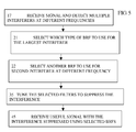
- Figure 5 shows steps for another embodiment, which could be carried out by the receiver of figure 1 or 3 or other embodiment.
- the signal is received and multiple interferers are detected at different frequencies. This can involve detecting the strongest interferer and then determining if there are other major interferers, by using other thresholds. If so then it may be more effective to use the different types of BRFs for different interferers.
- a selection is made of which BRF to use for the largest interferer. This can be for example the analog BRF, if the interferer is strong enough.
- another BRF is selected to use for suppressing the second largest interferer at a different frequency.
- the selected BRFs are tuned to suppress the detected interference.
- the useful signal is received by the receiver circuitry with the interference suppressed using the selected BRFs.
- a schematic view of an example of a receiver shows an analog part 500 and a digital part 565.
- the analog part is an antenna feeding an analog front end 505.
- This can include a mixer and LO, adaptable to receive a different range of frequencies.
- the front end feeds a tunable BRF 510.
- This feeds a gain control part 520.
- the output of this is fed to the ADC 340.
- the BRF optionally has a bypass path so that it is switched out during detection of the interference.
- the ADC feeds digital signals to the digital part 565.
- This can include digital logic 249 for carrying out various processing functions including power detection to provide a measure of maximum power to feed back a control signal to the gain control part.
- the digital part can also include a FFT part 535.
- This FFT part forms a spectral analyzer for use in the interference detector 130.
- Other logic is used to process the resulting spectrum to detect the interference.
- Further logic 249 can be used to carry out the BRF selection and tuning control to feedback to the tunable analog BRF.
- the FFT can feed subsequent digital baseband parts, shown by a block 251 for synchronisation, IFFT and or other processing as needed for the application. If appropriate, the FFT can be bypassed so the digital baseband has access to the time domain information, for deriving the useful signal.
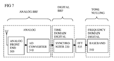
- FIG. 7 schematic view of a wireless receiver having a synchronizer and multiple BRFs
- Figure 7 shows another embodiment of a wireless receiver having three different types of BRF; an analog BRF, a digital time domain BRF and a digital frequency domain BRF (tone nulling).
- the locations of these parts in the receiver chain are shown in figure 7 .
- the analog BRF can be in the analog dotted line box, where the chain has the analog front end 505 and the ADC 340.
- the digital time domain BRF can be in the time domain digital part, where there can be a synchronizer 220 in a typical receiver.
- After the FFT 535 is the frequency domain part, which also has the baseband part 540.
- the frequency domain BRF in the form of a tone nulling circuit can be in this part of the chain.
- the analog filter requirements can be simplified by providing additional interference suppression mechanisms in the digital part of the system. The working can be understood from the following analysis of the problem. It is also feasible to have embodiments with no analog BRF, relying on the different types of digital BRF.
- Fig. 8 schematic view of receiver circuitry having tone nulling
- Figure 8 shows another embodiment of a receiver, similar to that of figure 6 and also having additional parts in the digital side.
- a tunable digital BRF and gain section 380 receive the digital samples from the ADC. After the FFT is a tone nulling section 360 followed by other digital baseband processing, 251.
- the digital logic section 237 can provide power detection and control of digital or analog gain control parts as well as providing the selection and tuning of the different types of BRFs.
- the steps of the embodiment of figure 9 can represent the operations of the embodiment of figs 1 , 3 , 6 , 7 , 8 or other embodiment.
- a signal is received, having the useful signal in a particular band.
- the receiver circuitry operates to receive (meaning distinguish) the particular band, and the interference detector detects the interference.
- Such detection can be carried out in various ways, one of which will be described in more detail below.
- Steps 27, 37, 47 and 57 correspond to steps 25 and 35 of figure 2 , in which a selection is made between the different types of BRFs, according to the interference detection, to provide a more appropriate or efficient match of the BRF to the interference. This can involve the following steps.
- the largest interferer is found.
- a digital filter only is used, otherwise the analog filter is tuned to the largest interferer.
- time domain synchronisation is working, then only the frequency domain digital filter is used.
- time domain digital filter is tuned for the second interferer.
- the analog filter is tuned to the frequency and optionally to the bandwidth and strength of the detected interference.
- the residual interference can be measured or estimated and the digital filter or filters can be tuned to the residual interference or to some other interferer.
- the useful signal is received with interference suppressed using the selected filters.
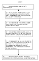
- steps are shown for use in the receiver of figs 1 , 3 , 6 , 7 , 8 or other embodiment, this time involving three types of BRF, an analog BRF, a digital time domain BRF, and a digital frequency domain BRF.
- interferers are detected.
- step 905 whether the interference is above a first threshold is determined. If so, the analog BRF is selected and tuned. Otherwise at step 920, whether synchronisation is achieved is checked. If not, then at step 925, the digital time domain BRF is selected and tuned. Otherwise this is bypassed and at step 930, the conversion to frequency domain is carried out.
- step 915 optionally interferers are detected again and if found at step 935, then the frequency domain filtering is selected and tuned so that the appropriate frequency bins are nulled.
- step 800 the PSD is estimated from the FFT output using Bartlett's method.
- step 810 all the subcarriers with a power larger than a threshold times the mean over all carriers are found.
- step 820 if the distance in frequency between subcarriers over this power is larger than a constant, they are taken to be separate interferers.
- step 830 a centre frequency of each interferer is determined. Then a power in the interval around the central subcarrier is determined at step 840.
- Some of the method steps discussed above for determining parameters, or comparing parameters to thresholds, or selecting and tuning filters for example, may be implemented by logic in the form of hardware or, for example, in software using a processing engine such as a microprocessor or a programmable logic device (PLD's) such as a PLA (programmable logic array), PAL (programmable array logic), FPGA (field programmable gate array).
- PLD's programmable logic device
- PLA programmable logic array
- PAL programmable array logic
- FPGA field programmable gate array
- An example of a circuit with an embedded processor will be described for use mobile radio telephone receiver/transceiver. This circuit may be constructed as a VLSI chip around an embedded microprocessor such as an ARM7TDMI core designed by ARM Ltd., UK which may be synthesized onto a single chip with the other components shown.
- processors may be used and these need not be embedded, e.g. a Pentium processor as supplied by Intel Corp. USA.
- a zero wait state SRAM memory may be provided on-chip as well as a cache memory for example.
- I/O (input/output) interfaces are provided for receiving and transmitting data to the relevant networks, e.g. a data or speech information, wireless or cable networks.
- FIFO buffers may be used to decouple the processor from data transfer through these interfaces.
- the interface can provide network connections, i.e. suitable ports and network addresses, e.g. the interfaces may be in the form of network cards.
- One interface can provide a wireless front end for receiving wireless transmissions from a wireless network.
- Software programs may be stored in an internal ROM (read only memory) and/or on any other non-volatile memory, e.g. they may be stored on an internal non-volatile memory such as a hard disc or solid state memory or in an external memory. Access to an external memory may be provided an external bus interface if needed, with address, data and control busses.
- the methods and/or receiver of the present invention may be implemented as software to run on a processor. In particular a receiver in accordance with the present invention may be implemented by suitable programming of the processor.
- the methods and procedures described above may be written as computer programs in a suitable computer language such as C and then compiled for the specific processor in the embedded design.
- the software may be written in C and then compiled using the ARM C compiler and the ARM assembler.
- the software has code, which when executed on a processing engine provides the methods and/or the wireless receiver of the present invention.
- the software programs may be stored on any suitable machine readable medium such as magnetic disks, diskettes, solid state memory, tape memory, optical disks such as CD-ROM or DVD-ROM, etc. Other variations can be envisaged within the scope of the claims.
Landscapes
- Engineering & Computer Science (AREA)
- Computer Networks & Wireless Communication (AREA)
- Signal Processing (AREA)
- Noise Elimination (AREA)
Priority Applications (3)
| Application Number | Priority Date | Filing Date | Title |
|---|---|---|---|
| EP20100164466 EP2391024B1 (de) | 2010-05-31 | 2010-05-31 | Filtern von erkannten Störungen in einem drahtlosen Empfänger |
| PCT/EP2011/058082 WO2011151182A1 (en) | 2010-05-31 | 2011-05-18 | Filtering interference detected at wireless receiver |
| US13/695,473 US8818314B2 (en) | 2010-05-31 | 2011-05-18 | Filtering interference detected at wireless receiver |
Applications Claiming Priority (1)
| Application Number | Priority Date | Filing Date | Title |
|---|---|---|---|
| EP20100164466 EP2391024B1 (de) | 2010-05-31 | 2010-05-31 | Filtern von erkannten Störungen in einem drahtlosen Empfänger |
Publications (2)
| Publication Number | Publication Date |
|---|---|
| EP2391024A1 true EP2391024A1 (de) | 2011-11-30 |
| EP2391024B1 EP2391024B1 (de) | 2014-05-14 |
Family
ID=42371479
Family Applications (1)
| Application Number | Title | Priority Date | Filing Date |
|---|---|---|---|
| EP20100164466 Not-in-force EP2391024B1 (de) | 2010-05-31 | 2010-05-31 | Filtern von erkannten Störungen in einem drahtlosen Empfänger |
Country Status (3)
| Country | Link |
|---|---|
| US (1) | US8818314B2 (de) |
| EP (1) | EP2391024B1 (de) |
| WO (1) | WO2011151182A1 (de) |
Cited By (5)
| Publication number | Priority date | Publication date | Assignee | Title |
|---|---|---|---|---|
| GB2487225A (en) * | 2011-01-14 | 2012-07-18 | Icera Inc | Wireless receiver having plural receiver processors selected for a time based on a comparison of quality measures of their respective outputs |
| WO2017023544A1 (en) * | 2015-08-06 | 2017-02-09 | Qualcomm Incorporated | Dynamic selection of analog interference cancellers |
| WO2017039819A1 (en) * | 2015-09-04 | 2017-03-09 | Raytheon Company | Apparatus and method for selective signal cancellation |
| CN113078916A (zh) * | 2021-03-26 | 2021-07-06 | 长沙驰芯半导体科技有限公司 | 一种超宽带接收机抑制干扰电路及抑制干扰的方法 |
| WO2024114925A1 (en) * | 2022-12-02 | 2024-06-06 | Nokia Technologies Oy | Analog-digital filtering |
Families Citing this family (8)
| Publication number | Priority date | Publication date | Assignee | Title |
|---|---|---|---|---|
| US11265118B2 (en) * | 2013-06-26 | 2022-03-01 | Maxlinear Asia Singapore Private Limited | Spectrum analyzer integrated in a point-to-point outdoor unit |
| TWI610545B (zh) * | 2016-06-21 | 2018-01-01 | 晨星半導體股份有限公司 | 檢測凹口頻帶之檢測方法及檢測裝置 |
| US9628122B1 (en) * | 2016-07-25 | 2017-04-18 | The Aerospace Corporation | Circuits and methods for reducing interference that spectrally overlaps a desired signal based on dynamic gain control and/or equalization |
| US10536225B2 (en) * | 2018-02-06 | 2020-01-14 | Arris Enterprises Llc | Reducing wireless interference from a wired digital interface |
| US11121785B2 (en) * | 2019-01-10 | 2021-09-14 | Exfo Inc. | Detection and tracking of interferers in a RF spectrum with multi-lane processing |
| US11540234B2 (en) | 2019-12-05 | 2022-12-27 | Exfo Inc. | Automated narrow peak interference severity estimation |
| IL280268B (en) | 2021-01-15 | 2022-08-01 | Rafael Advanced Defense Systems Ltd | Interference rejection broadband receiver |
| US11929774B1 (en) * | 2022-11-08 | 2024-03-12 | Changsha Chixin Semiconductor Tech Co., Ltd. | Adaptive method for multi-order multi-band anti-interference intelligent UWB antenna |
Citations (5)
| Publication number | Priority date | Publication date | Assignee | Title |
|---|---|---|---|---|
| US20070140381A1 (en) * | 2004-04-27 | 2007-06-21 | Mitsubishi Electric Corporation | Wireless apparatus |
| EP1956719A2 (de) * | 2007-02-09 | 2008-08-13 | Matsushita Electric Industrial Co., Ltd. | Funkempfangsvorrichtung |
| WO2009114123A2 (en) | 2008-03-10 | 2009-09-17 | Newlans, Inc. | Method, system, and apparatus for wideband signal processeing |
| WO2010018492A1 (en) | 2008-08-13 | 2010-02-18 | Nxp B.V. | Wide band transceiver and data receiving method using a tunable notch filter and pre-estimated optimal notch filter parameters |
| WO2010046798A1 (en) * | 2008-10-23 | 2010-04-29 | Nxp B.V. | System and method for adaptive radio frequency filtering |
Family Cites Families (1)
| Publication number | Priority date | Publication date | Assignee | Title |
|---|---|---|---|---|
| JP4000088B2 (ja) * | 2003-05-09 | 2007-10-31 | 松下電器産業株式会社 | 無線受信装置および受信フィルタリング方法 |
-
2010
- 2010-05-31 EP EP20100164466 patent/EP2391024B1/de not_active Not-in-force
-
2011
- 2011-05-18 WO PCT/EP2011/058082 patent/WO2011151182A1/en not_active Ceased
- 2011-05-18 US US13/695,473 patent/US8818314B2/en not_active Expired - Fee Related
Patent Citations (5)
| Publication number | Priority date | Publication date | Assignee | Title |
|---|---|---|---|---|
| US20070140381A1 (en) * | 2004-04-27 | 2007-06-21 | Mitsubishi Electric Corporation | Wireless apparatus |
| EP1956719A2 (de) * | 2007-02-09 | 2008-08-13 | Matsushita Electric Industrial Co., Ltd. | Funkempfangsvorrichtung |
| WO2009114123A2 (en) | 2008-03-10 | 2009-09-17 | Newlans, Inc. | Method, system, and apparatus for wideband signal processeing |
| WO2010018492A1 (en) | 2008-08-13 | 2010-02-18 | Nxp B.V. | Wide band transceiver and data receiving method using a tunable notch filter and pre-estimated optimal notch filter parameters |
| WO2010046798A1 (en) * | 2008-10-23 | 2010-04-29 | Nxp B.V. | System and method for adaptive radio frequency filtering |
Cited By (7)
| Publication number | Priority date | Publication date | Assignee | Title |
|---|---|---|---|---|
| GB2487225A (en) * | 2011-01-14 | 2012-07-18 | Icera Inc | Wireless receiver having plural receiver processors selected for a time based on a comparison of quality measures of their respective outputs |
| GB2487225B (en) * | 2011-01-14 | 2017-12-06 | Nvidia Tech Uk Limited | Receiving an input signal over a channel of a wireless network |
| WO2017023544A1 (en) * | 2015-08-06 | 2017-02-09 | Qualcomm Incorporated | Dynamic selection of analog interference cancellers |
| WO2017039819A1 (en) * | 2015-09-04 | 2017-03-09 | Raytheon Company | Apparatus and method for selective signal cancellation |
| CN113078916A (zh) * | 2021-03-26 | 2021-07-06 | 长沙驰芯半导体科技有限公司 | 一种超宽带接收机抑制干扰电路及抑制干扰的方法 |
| CN113078916B (zh) * | 2021-03-26 | 2022-04-15 | 长沙驰芯半导体科技有限公司 | 一种超宽带接收机抑制干扰电路及抑制干扰的方法 |
| WO2024114925A1 (en) * | 2022-12-02 | 2024-06-06 | Nokia Technologies Oy | Analog-digital filtering |
Also Published As
| Publication number | Publication date |
|---|---|
| US20130045705A1 (en) | 2013-02-21 |
| US8818314B2 (en) | 2014-08-26 |
| WO2011151182A1 (en) | 2011-12-08 |
| EP2391024B1 (de) | 2014-05-14 |
Similar Documents
| Publication | Publication Date | Title |
|---|---|---|
| EP2391024B1 (de) | Filtern von erkannten Störungen in einem drahtlosen Empfänger | |
| US9100084B2 (en) | Synchronizing and detecting interference in wireless receiver | |
| US8655300B2 (en) | Detecting interference in wireless receiver | |
| US8855592B2 (en) | Arrangements for narrow band interference detection | |
| JP5562981B2 (ja) | 周波数スペクトル情報に応答する調整可能受信フィルタ | |
| US20080125046A1 (en) | Transmission system with interference avoidance capability and method thereof | |
| JP2008235978A (ja) | 通信装置 | |
| EP3090489B1 (de) | Verfahren zur einstellung von lo-frequenzen bei einem empfänger und zugehöriger empfänger | |
| JP5551716B2 (ja) | 調整可能送信フィルタ | |
| KR20160106665A (ko) | Rx 다이버시티 안테나를 사용하는 기회적 액티브 간섭 소거 | |
| US20180017663A1 (en) | Detecting federal incumbent radar (fir) signal | |
| CN101807960A (zh) | 基于小波包变换实现自适应频谱感知的方法 | |
| JP2016106447A (ja) | 調整可能受信フィルタ | |
| CN105703784B (zh) | 谐波杂散抑制的方法和设备接收机 | |
| JP4123433B2 (ja) | Uwb受信方法及びuwb受信装置 | |
| GB2523856A (en) | Method and apparatus for agile wire | |
| Arslan et al. | Narrowband interference issues in ultra wideband systems | |
| KR100892859B1 (ko) | 초광대역 통신시스템에서의 논블라인드 방식에 의한 희생원검출방법 | |
| KR20090121144A (ko) | 하이브리드 첩 펄스 정형화를 이용한 다중대역 uwb시스템 및 협대역 간섭 소거 방법. |
Legal Events
| Date | Code | Title | Description |
|---|---|---|---|
| AK | Designated contracting states |
Kind code of ref document: A1 Designated state(s): AL AT BE BG CH CY CZ DE DK EE ES FI FR GB GR HR HU IE IS IT LI LT LU LV MC MK MT NL NO PL PT RO SE SI SK SM TR |
|
| AX | Request for extension of the european patent |
Extension state: BA ME RS |
|
| PUAI | Public reference made under article 153(3) epc to a published international application that has entered the european phase |
Free format text: ORIGINAL CODE: 0009012 |
|
| RIN1 | Information on inventor provided before grant (corrected) |
Inventor name: KAPOOR, AJAY Inventor name: STASSEN, MAURICE |
|
| 17P | Request for examination filed |
Effective date: 20120510 |
|
| 17Q | First examination report despatched |
Effective date: 20120809 |
|
| GRAP | Despatch of communication of intention to grant a patent |
Free format text: ORIGINAL CODE: EPIDOSNIGR1 |
|
| INTG | Intention to grant announced |
Effective date: 20140212 |
|
| GRAS | Grant fee paid |
Free format text: ORIGINAL CODE: EPIDOSNIGR3 |
|
| GRAA | (expected) grant |
Free format text: ORIGINAL CODE: 0009210 |
|
| AK | Designated contracting states |
Kind code of ref document: B1 Designated state(s): AL AT BE BG CH CY CZ DE DK EE ES FI FR GB GR HR HU IE IS IT LI LT LU LV MC MK MT NL NO PL PT RO SE SI SK SM TR |
|
| REG | Reference to a national code |
Ref country code: GB Ref legal event code: FG4D |
|
| REG | Reference to a national code |
Ref country code: AT Ref legal event code: REF Ref document number: 668954 Country of ref document: AT Kind code of ref document: T Effective date: 20140615 |
|
| REG | Reference to a national code |
Ref country code: IE Ref legal event code: FG4D Ref country code: DE Ref legal event code: R096 Ref document number: 602010016040 Country of ref document: DE Effective date: 20140618 |
|
| REG | Reference to a national code |
Ref country code: NL Ref legal event code: VDEP Effective date: 20140514 Ref country code: AT Ref legal event code: MK05 Ref document number: 668954 Country of ref document: AT Kind code of ref document: T Effective date: 20140514 |
|
| REG | Reference to a national code |
Ref country code: LT Ref legal event code: MG4D |
|
| PG25 | Lapsed in a contracting state [announced via postgrant information from national office to epo] |
Ref country code: FI Free format text: LAPSE BECAUSE OF FAILURE TO SUBMIT A TRANSLATION OF THE DESCRIPTION OR TO PAY THE FEE WITHIN THE PRESCRIBED TIME-LIMIT Effective date: 20140514 Ref country code: GR Free format text: LAPSE BECAUSE OF FAILURE TO SUBMIT A TRANSLATION OF THE DESCRIPTION OR TO PAY THE FEE WITHIN THE PRESCRIBED TIME-LIMIT Effective date: 20140815 Ref country code: IS Free format text: LAPSE BECAUSE OF FAILURE TO SUBMIT A TRANSLATION OF THE DESCRIPTION OR TO PAY THE FEE WITHIN THE PRESCRIBED TIME-LIMIT Effective date: 20140914 Ref country code: LT Free format text: LAPSE BECAUSE OF FAILURE TO SUBMIT A TRANSLATION OF THE DESCRIPTION OR TO PAY THE FEE WITHIN THE PRESCRIBED TIME-LIMIT Effective date: 20140514 Ref country code: CY Free format text: LAPSE BECAUSE OF FAILURE TO SUBMIT A TRANSLATION OF THE DESCRIPTION OR TO PAY THE FEE WITHIN THE PRESCRIBED TIME-LIMIT Effective date: 20140514 Ref country code: NO Free format text: LAPSE BECAUSE OF FAILURE TO SUBMIT A TRANSLATION OF THE DESCRIPTION OR TO PAY THE FEE WITHIN THE PRESCRIBED TIME-LIMIT Effective date: 20140814 |
|
| PG25 | Lapsed in a contracting state [announced via postgrant information from national office to epo] |
Ref country code: PL Free format text: LAPSE BECAUSE OF FAILURE TO SUBMIT A TRANSLATION OF THE DESCRIPTION OR TO PAY THE FEE WITHIN THE PRESCRIBED TIME-LIMIT Effective date: 20140514 Ref country code: SE Free format text: LAPSE BECAUSE OF FAILURE TO SUBMIT A TRANSLATION OF THE DESCRIPTION OR TO PAY THE FEE WITHIN THE PRESCRIBED TIME-LIMIT Effective date: 20140514 Ref country code: ES Free format text: LAPSE BECAUSE OF FAILURE TO SUBMIT A TRANSLATION OF THE DESCRIPTION OR TO PAY THE FEE WITHIN THE PRESCRIBED TIME-LIMIT Effective date: 20140514 Ref country code: LV Free format text: LAPSE BECAUSE OF FAILURE TO SUBMIT A TRANSLATION OF THE DESCRIPTION OR TO PAY THE FEE WITHIN THE PRESCRIBED TIME-LIMIT Effective date: 20140514 Ref country code: HR Free format text: LAPSE BECAUSE OF FAILURE TO SUBMIT A TRANSLATION OF THE DESCRIPTION OR TO PAY THE FEE WITHIN THE PRESCRIBED TIME-LIMIT Effective date: 20140514 Ref country code: AT Free format text: LAPSE BECAUSE OF FAILURE TO SUBMIT A TRANSLATION OF THE DESCRIPTION OR TO PAY THE FEE WITHIN THE PRESCRIBED TIME-LIMIT Effective date: 20140514 |
|
| PG25 | Lapsed in a contracting state [announced via postgrant information from national office to epo] |
Ref country code: PT Free format text: LAPSE BECAUSE OF FAILURE TO SUBMIT A TRANSLATION OF THE DESCRIPTION OR TO PAY THE FEE WITHIN THE PRESCRIBED TIME-LIMIT Effective date: 20140915 |
|
| REG | Reference to a national code |
Ref country code: CH Ref legal event code: PL |
|
| PG25 | Lapsed in a contracting state [announced via postgrant information from national office to epo] |
Ref country code: SK Free format text: LAPSE BECAUSE OF FAILURE TO SUBMIT A TRANSLATION OF THE DESCRIPTION OR TO PAY THE FEE WITHIN THE PRESCRIBED TIME-LIMIT Effective date: 20140514 Ref country code: LI Free format text: LAPSE BECAUSE OF NON-PAYMENT OF DUE FEES Effective date: 20140531 Ref country code: EE Free format text: LAPSE BECAUSE OF FAILURE TO SUBMIT A TRANSLATION OF THE DESCRIPTION OR TO PAY THE FEE WITHIN THE PRESCRIBED TIME-LIMIT Effective date: 20140514 Ref country code: CZ Free format text: LAPSE BECAUSE OF FAILURE TO SUBMIT A TRANSLATION OF THE DESCRIPTION OR TO PAY THE FEE WITHIN THE PRESCRIBED TIME-LIMIT Effective date: 20140514 Ref country code: DK Free format text: LAPSE BECAUSE OF FAILURE TO SUBMIT A TRANSLATION OF THE DESCRIPTION OR TO PAY THE FEE WITHIN THE PRESCRIBED TIME-LIMIT Effective date: 20140514 Ref country code: RO Free format text: LAPSE BECAUSE OF FAILURE TO SUBMIT A TRANSLATION OF THE DESCRIPTION OR TO PAY THE FEE WITHIN THE PRESCRIBED TIME-LIMIT Effective date: 20140514 Ref country code: CH Free format text: LAPSE BECAUSE OF NON-PAYMENT OF DUE FEES Effective date: 20140531 Ref country code: BE Free format text: LAPSE BECAUSE OF FAILURE TO SUBMIT A TRANSLATION OF THE DESCRIPTION OR TO PAY THE FEE WITHIN THE PRESCRIBED TIME-LIMIT Effective date: 20140514 |
|
| REG | Reference to a national code |
Ref country code: DE Ref legal event code: R097 Ref document number: 602010016040 Country of ref document: DE |
|
| REG | Reference to a national code |
Ref country code: IE Ref legal event code: MM4A |
|
| PG25 | Lapsed in a contracting state [announced via postgrant information from national office to epo] |
Ref country code: NL Free format text: LAPSE BECAUSE OF FAILURE TO SUBMIT A TRANSLATION OF THE DESCRIPTION OR TO PAY THE FEE WITHIN THE PRESCRIBED TIME-LIMIT Effective date: 20140514 |
|
| PLBE | No opposition filed within time limit |
Free format text: ORIGINAL CODE: 0009261 |
|
| STAA | Information on the status of an ep patent application or granted ep patent |
Free format text: STATUS: NO OPPOSITION FILED WITHIN TIME LIMIT |
|
| REG | Reference to a national code |
Ref country code: FR Ref legal event code: ST Effective date: 20150303 |
|
| 26N | No opposition filed |
Effective date: 20150217 |
|
| PG25 | Lapsed in a contracting state [announced via postgrant information from national office to epo] |
Ref country code: IE Free format text: LAPSE BECAUSE OF NON-PAYMENT OF DUE FEES Effective date: 20140531 Ref country code: IT Free format text: LAPSE BECAUSE OF FAILURE TO SUBMIT A TRANSLATION OF THE DESCRIPTION OR TO PAY THE FEE WITHIN THE PRESCRIBED TIME-LIMIT Effective date: 20140514 |
|
| REG | Reference to a national code |
Ref country code: DE Ref legal event code: R097 Ref document number: 602010016040 Country of ref document: DE Effective date: 20150217 |
|
| PG25 | Lapsed in a contracting state [announced via postgrant information from national office to epo] |
Ref country code: FR Free format text: LAPSE BECAUSE OF NON-PAYMENT OF DUE FEES Effective date: 20140715 |
|
| PG25 | Lapsed in a contracting state [announced via postgrant information from national office to epo] |
Ref country code: SI Free format text: LAPSE BECAUSE OF FAILURE TO SUBMIT A TRANSLATION OF THE DESCRIPTION OR TO PAY THE FEE WITHIN THE PRESCRIBED TIME-LIMIT Effective date: 20140514 |
|
| PG25 | Lapsed in a contracting state [announced via postgrant information from national office to epo] |
Ref country code: MT Free format text: LAPSE BECAUSE OF FAILURE TO SUBMIT A TRANSLATION OF THE DESCRIPTION OR TO PAY THE FEE WITHIN THE PRESCRIBED TIME-LIMIT Effective date: 20140514 |
|
| PG25 | Lapsed in a contracting state [announced via postgrant information from national office to epo] |
Ref country code: MC Free format text: LAPSE BECAUSE OF FAILURE TO SUBMIT A TRANSLATION OF THE DESCRIPTION OR TO PAY THE FEE WITHIN THE PRESCRIBED TIME-LIMIT Effective date: 20140514 Ref country code: SM Free format text: LAPSE BECAUSE OF FAILURE TO SUBMIT A TRANSLATION OF THE DESCRIPTION OR TO PAY THE FEE WITHIN THE PRESCRIBED TIME-LIMIT Effective date: 20140514 |
|
| PG25 | Lapsed in a contracting state [announced via postgrant information from national office to epo] |
Ref country code: BG Free format text: LAPSE BECAUSE OF FAILURE TO SUBMIT A TRANSLATION OF THE DESCRIPTION OR TO PAY THE FEE WITHIN THE PRESCRIBED TIME-LIMIT Effective date: 20140514 |
|
| PG25 | Lapsed in a contracting state [announced via postgrant information from national office to epo] |
Ref country code: HU Free format text: LAPSE BECAUSE OF FAILURE TO SUBMIT A TRANSLATION OF THE DESCRIPTION OR TO PAY THE FEE WITHIN THE PRESCRIBED TIME-LIMIT; INVALID AB INITIO Effective date: 20100531 Ref country code: TR Free format text: LAPSE BECAUSE OF FAILURE TO SUBMIT A TRANSLATION OF THE DESCRIPTION OR TO PAY THE FEE WITHIN THE PRESCRIBED TIME-LIMIT Effective date: 20140514 Ref country code: LU Free format text: LAPSE BECAUSE OF NON-PAYMENT OF DUE FEES Effective date: 20140531 |
|
| REG | Reference to a national code |
Ref country code: DE Ref legal event code: R081 Ref document number: 602010016040 Country of ref document: DE Owner name: OCT CIRCUIT TECHNOLOGIES INTERNATIONAL LTD., IE Free format text: FORMER OWNER: ST-ERICSSON SA, PLAN-LES-OUATES, CH |
|
| PG25 | Lapsed in a contracting state [announced via postgrant information from national office to epo] |
Ref country code: MK Free format text: LAPSE BECAUSE OF FAILURE TO SUBMIT A TRANSLATION OF THE DESCRIPTION OR TO PAY THE FEE WITHIN THE PRESCRIBED TIME-LIMIT Effective date: 20140514 |
|
| PG25 | Lapsed in a contracting state [announced via postgrant information from national office to epo] |
Ref country code: AL Free format text: LAPSE BECAUSE OF FAILURE TO SUBMIT A TRANSLATION OF THE DESCRIPTION OR TO PAY THE FEE WITHIN THE PRESCRIBED TIME-LIMIT Effective date: 20140514 |
|
| REG | Reference to a national code |
Ref country code: GB Ref legal event code: 732E Free format text: REGISTERED BETWEEN 20210722 AND 20210728 |
|
| REG | Reference to a national code |
Ref country code: GB Ref legal event code: 732E Free format text: REGISTERED BETWEEN 20210805 AND 20210811 |
|
| PGFP | Annual fee paid to national office [announced via postgrant information from national office to epo] |
Ref country code: GB Payment date: 20220527 Year of fee payment: 13 Ref country code: DE Payment date: 20220527 Year of fee payment: 13 |
|
| REG | Reference to a national code |
Ref country code: DE Ref legal event code: R119 Ref document number: 602010016040 Country of ref document: DE |
|
| GBPC | Gb: european patent ceased through non-payment of renewal fee |
Effective date: 20230531 |
|
| PG25 | Lapsed in a contracting state [announced via postgrant information from national office to epo] |
Ref country code: DE Free format text: LAPSE BECAUSE OF NON-PAYMENT OF DUE FEES Effective date: 20231201 Ref country code: GB Free format text: LAPSE BECAUSE OF NON-PAYMENT OF DUE FEES Effective date: 20230531 |