EP2391001B1 - Einführung einer komplexen Abtastung - Google Patents
Einführung einer komplexen Abtastung Download PDFInfo
- Publication number
- EP2391001B1 EP2391001B1 EP11161952.4A EP11161952A EP2391001B1 EP 2391001 B1 EP2391001 B1 EP 2391001B1 EP 11161952 A EP11161952 A EP 11161952A EP 2391001 B1 EP2391001 B1 EP 2391001B1
- Authority
- EP
- European Patent Office
- Prior art keywords
- frequency
- domain
- signal
- sampling
- delayed
- Prior art date
- Legal status (The legal status is an assumption and is not a legal conclusion. Google has not performed a legal analysis and makes no representation as to the accuracy of the status listed.)
- Active
Links
Images


Classifications
-
- H—ELECTRICITY
- H04—ELECTRIC COMMUNICATION TECHNIQUE
- H04L—TRANSMISSION OF DIGITAL INFORMATION, e.g. TELEGRAPHIC COMMUNICATION
- H04L27/00—Modulated-carrier systems
- H04L27/32—Carrier systems characterised by combinations of two or more of the types covered by groups H04L27/02, H04L27/10, H04L27/18 or H04L27/26
- H04L27/34—Amplitude- and phase-modulated carrier systems, e.g. quadrature-amplitude modulated carrier systems
- H04L27/38—Demodulator circuits; Receiver circuits
- H04L27/3845—Demodulator circuits; Receiver circuits using non - coherent demodulation, i.e. not using a phase synchronous carrier
- H04L27/3854—Demodulator circuits; Receiver circuits using non - coherent demodulation, i.e. not using a phase synchronous carrier using a non - coherent carrier, including systems with baseband correction for phase or frequency offset
- H04L27/3863—Compensation for quadrature error in the received signal
Definitions
- the present invention relates to digital signal processing. More particularly, the present invention relates to a method and system for performing complex sampling of signals by using two or more sampling channels (second-order sampling or higher) and calculating corresponding time delays between the two or more sampling channels.
- bandpass signals signals that are used in many applications are, in many cases, band limited to a predefined frequency interval, and thus these signals are called bandpass signals.
- a uniform sampling theorem for bandpass signal is known from the prior art, and its analysis is usually based on the time frequency equivalence.
- A. W. Kohlenberg proposed the second order sampling for a bandpass signal (in the article titled “Exact interpolation of band-limited functions", published in the journal of Applied Physics, in 1953, issue 24(12), pages 1432-1436 ), which is considered to be the simplest case of non-uniform sampling where two uniform sampling sequences are interleaved.
- Second order sampling allows the theoretical minimal sampling rate of two-times bandwidth, in the form of an average rate, to be applied independent of the band position.
- the signal can be fully reconstructed (e.g., by performing signal interpolation) even when the signal frequency range contains whole multiples or half-multiples of the sampling frequency.
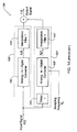
- Fig. 1A schematically illustrates a conventional interpolation system 100 of second order sampling, according to the prior art.
- the input signal X(t) ( t is a time parameter) passes through two Analog-to-Digital (A/D) converters 105' and 105" with a predefined time delay ⁇ between them.
- A/D Analog-to-Digital
- the converted signals X 1 (l) and X 2 ( l ) are inputted into interpolation filters 110' and 110", respectively, for performing signal interpolation, which includes digital to analog conversion.
- the resulting interpolated signals are summed together, giving rise to the output signal Y(l) , and in turn Y(t) .
- Valkama et al. in the article titled “A Novel Image Rejection Architecture for Quadrature Radio Receivers” published in the "IEEE Transactions on Circuits and Systems” journal (volume 51, number 2, pp. 61-68, February 2004 ), presents a novel structure for obtaining an image-free baseband observation of the received bandpass signal by utilizing I/Q (Inphase/Quadrature) signal processing. The phase difference between I and Q branches is approximated by a relative time delay of one quarter of the carrier cycle. Also, Valkama et al. presents and analyzes an analog delay processing based model, and then determines the obtainable image rejection of the delay processing. In addition, Valkama et al.
- the conventional complex signal processing is also used in processing schemes where an input signal is bandpass in its origin, and is to be processed in a lowpass form. This normally requires two-channel processing in quadrature channels to remove an ambiguity as to whether a signal is higher or lower than the bandpass center frequency.
- the complex signal processing can be extended to the digital signal processing field, and the processed signal can be first mixed to zero-center frequency in two quadrature channels, then filtered to remove the high frequency mixing products, and after that digitized by a number of A/D (Analog-to-Digital) converters.
- FIG. 1B schematically illustrates a conventional complex sampling system 160, in which an input signal is sampled in two sampling channels 150' and 150", while shifting the phase by ninety degrees.
- a complex signal is obtained, said signal having a real part Re ⁇ X(l) ⁇ and an imaginary part Im ⁇ X(l) ⁇ , wherein parameter l represents a series of discrete values.
- Filters 151, 152' and 152" are used to filter the undesired frequency range (in a time domain) of input signals X(t), X 1 '(t) and X 2 '(t), respectively.
- US 5,099,194 discloses an approach to extending the frequency range uses non-uniform sampling to gain the advantages of a high sampling rate with only a modest increase in the number of samples.
- Two sets of uniform samples with slightly different sampling frequency are used. Each set of samples is Fourier transformed independently and the frequency of the lowest aliases determined. It is shown that knowledge of these two alias frequencies permits unambiguous determination of the signal frequency over a range far exceeding the Nyquist frequency, except at a discrete set of points.
- US 5,099,243 presents a technique for extending the frequency range which employs in-phase and quadrature components of the signal coupled with non-uniform sampling to gain the advantages of a high sampling rate with only a small increase in the number of samples.
- a quadrature IF signal can be generated. Both in-phase and quadrature components are sampled and the samples are combined to form a complex signal.
- this signal is transformed, only one alias is obtained per periodic repetition and the effective Nyquist frequency is doubled.
- Two sets of complex samples are then used with the slightly different sampling frequency. Each set is independently Fourier transformed and the frequency of the lowest aliases permits unambiguous determination of the signal frequency over a range far exceeding the Nyquist frequency.
- US 5,109,188 teaches a technique for extending the frequency range which employs a power divider having two outputs, one output being supplied to a first Analog-to-Digital (A/D) converter, and the other output being supplied via a delay device to a second A/D converter.
- a processor receives the outputs of the two A/D converters.
- the input signal is subjected to a known delay and both original and delayed signals are sampled simultaneously. Both sampled signals are Fourier transformed and the phase and amplitudes calculated. The phase difference between the original and delayed signals is also calculated, and an approximation to the true frequency for each peak observed in the amplitude spectrum is estimated.
- the present invention relates to a method and system for performing complex sampling of signals by using two or more sampling channels (second-order sampling or higher) and calculating corresponding time delays between the two or more sampling channels as defined in the independent claims.
- processing refers to the action and/or processes of a computer (machine) that manipulate and/or transform data into other data, said data represented as physical, e.g. such as electronic, quantities.
- the term "computer” should be expansively construed to cover any kind of electronic device with data processing capabilities, comprising, by the way of non-limiting examples, personal computers, servers, computing systems/units, communication devices, processors (e.g., digital signal processors (DSPs), microcontrollers, field programmable gate arrays (FPGAs), application specific integrated circuits (ASICs), etc.), and any other electronic computing devices.
- processors e.g., digital signal processors (DSPs), microcontrollers, field programmable gate arrays (FPGAs), application specific integrated circuits (ASICs), etc.
- operations in accordance with the teachings herein may be performed by a computer that is specially constructed for the desired purposes or by a general purpose computer that is specially configured for the desired purpose by means of a computer program stored in a computer readable storage medium.
- Fig. 2 is a schematic illustration 200 of complex sampling in a frequency domain by performing second-order sampling, according to an embodiment of the present invention.
- input signal X(t) is first filtered by means of filter 151 in order to remove the undesired frequency range (in a time domain).
- the filtered signal X 1 (t) is sampled by means of two sampling channels (systems/modules) 205' and 205", having a predefined time delay r between them, and then is converted to corresponding digital signals by means of conventional A/D converters 105' and 105", giving rise to X 1 (l) and X 2 (l) signals respectively.
- digital signals X 1 (l) and X 2 (l) are processed and converted to a frequency domain by means of the FFT (Fast Fourier Transform), which is a conventional technique for performing a discrete Fourier transform.
- FFT Fast Fourier Transform
- discrete signals X l '(k) and X 2 '(k) are obtained, wherein k is an index.
- the frequency band of input analog signal X(t) is known (the frequency bandwidth is equal to the sampling frequency Fs ), and therefore the phase difference of each frequency component of the delayed signal X 2 (k), which is provided via delayed sampling channel 205", can be calculated.
- the desired time delay r may be different for different frequency bands.
- the time delay ⁇ may be obtained either by providing time delay component/unit 103 (in which the time delay ⁇ can be predefined) or by performing a phase difference (e. g., a phase shift) of a sampling frequency, leading to a desired time delay of a signal.
- a phase difference e. g., a phase shift
- one or more phase and gain coefficients Q(k) 250 are used for (are applied to) each frequency component of signal X 2 '(k).
- These phase and gain coefficients Q(k) provided within the corresponding coefficients data unit 250, can be predefined, for example, empirically by substantially accurate measuring of the above time delay ⁇ . It should be noted that even in a case when time delay ⁇ is a frequency-dependent component, the corresponding phase and gain coefficients Q(k) can be still calculated and predefined thereof.
- the phase and gain coefficients are pre-calculated during the calibration process of system 200, and then are stored within the memory means (not shown), while there is a need for a coefficient for each frequency component of signal X 2 '(k), after applying the FFT transform. Further, for calculating the corresponding phase difference ⁇ ( k ), there is a need to provide a signal of a predefined frequency, and then calculate the corresponding phase difference ⁇ ( k ) between the delayed and reference signals X 2 '(k) and X 1 '(k) , respectively.
- the power ratio between two channels is calculated and corresponding gain coefficients g k ( k is an index) are determined and stored within memory means (not shown) for later usage.
- g k k is an index
- substantially all frequencies that correspond to the FFT frequency component to be calculated are provided, and then a phase difference for each such component is calculated.
- phase difference ⁇ between the sampling channels 205' and 205" is calculated.
- a number of frequencies are provided in intervals that are greater than the FFT bin ( bin is defined as F s / N , wherein N represents a number of FFT frequency components), and then the phase difference for each provided frequency is calculated by performing interpolation for each FFT frequency component.
- the phase difference ⁇ between the sampling channels 205' and 205" is calculated.
- phase differences ⁇ ( m ) between these frequencies are determined.
- the time delay ⁇ is calculated by using the above-determined phase differences ⁇ ( m ) by means of a novel method for calculating time delays between sampling channels (such as channels 205' and 205"), according to an embodiment of the present invention.
- a FFT bin is a single frequency of the FFT, to which each frequency component contributes
- f F s ⁇ n + k N
- f a signal frequency
- Fs is a sampling frequency
- N is the FFT length
- n is an integer
- k is a FFT bin number.
- an additional (for example, undesired) frequency component appears in the FFT bin (N-k), due to the symmetry of the conventional FFT.
- the phase difference ⁇ N-k of the above undesired frequency component has an opposite sign compared to the phase difference ⁇ k of the desired frequency component that appears in the FFT bin k .
- the frequency spectrum of the output signal Y(k) is equivalent to the frequency spectrum of the conventional complex sampling.
- an inverse frequency-domain transformation such as the Inverse Fourier transform (IFFT)
- IFFT Inverse Fourier transform
- time delays (time differences) between sampling channels can be calculated in a relatively accurate manner (for example, by means of a processing unit/system), as described below in detail.
- the first approximation of integer M can be determined, considering that 0 ⁇ ⁇ 1 ⁇ 2 ⁇ and 0 ⁇ ⁇ 2 ⁇ 2 ⁇ , and considering that ⁇ f is known.
- the range of time delays ⁇ can be selected in the following way. It is supposed, for example, that the frequencies are within the range of [ F start , F start + BW ], wherein F start is a starting frequency, and BW is a bandwidth, while Fs ⁇ BW ( Fs is a sampling frequency).
- phase difference ⁇ k 2 ⁇ ⁇ ⁇ n + k N ⁇ F s ⁇ ⁇
- n an integer
- ⁇ a time delay, which can be, for example, in the range determined by the following equation: 5 6 ⁇ 2 ⁇ n + 1 > F s ⁇ ⁇ > 1 6 ⁇ 2 ⁇ n - 1
- the delay ⁇ within the above range ensures that in addition to removing the undesired frequency component (FFT bin ( N-k )) of the frequency spectrum, the power of the desired frequency component (FFT bin k) will not be decreased more than 3dB (Decibels), as shown in the equation below: 10 ⁇ log 10 ⁇ 2 ⁇ sin ⁇ ⁇ ⁇ k + ⁇ ⁇ ⁇ N - k 2 2 > - 3 ⁇ dB wherein ⁇ k and ⁇ N-k are phase differences in bins k and ( N-k ), respectively.
- any other constraints can be considered, such as ensuring that the power of the desired frequency component will not be decreased, for example, more than 2dB (instead of 3dB), and the like.
- Fig. 3 is a schematic illustration of a complex sampling system 300, performing sampling in a time domain, according to another embodiment of the present invention.
- signal X 2 (l) passes through a digital FIR (Finite Impulse Response) filter unit 310.
- This filter is a complex filter and at its output, complex signal samples are obtained.
- the real part of the signal samples after FIR filter 310 is added to signal X 1 (l) that is outputted from A/D converter 105', giving rise to Re ⁇ Y(s) ⁇ signal, which is a real part of the signal, to which the complex sampling is applied.
- the imaginary part of the signal samples, after passing via the FIR filter 310 is the imaginary part ( Im ⁇ Y(s) ⁇ ) of the signal, to which the complex sampling is applied.
- IFFT inverse Fast Fourier transform
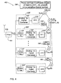
- Fig. 4 is a schematic illustration of a system 400 for complex sampling by performing sampling of the 2M -order sampling (the predefined-order sampling), according to still another embodiment of the present invention.
- 2M sampling channels two or more sampling channels
- F s is a sampling frequency.
- This can be compared to system 200 ( Fig. 2 ), for which signal bandwidth BW is less or equal to the sampling frequency: BW ⁇ F s .
- sampling channels 205', 205", etc. are represented by index n , while n ⁇ [1, 2M].
- the output frequency bands (Band 1, Band 2, etc.) are represented by index m , while m ⁇ [1, M ].
- each FFT bin is numbered by index k .
- the FFT of a signal is calculated in each sampling channel and is represented as X n ( k ), the output frequency spectrum is represented as Y m (k) , and phase and gain coefficients 250' are shown as Q m n k .
- input frequency F belongs to Band M if F ⁇ [ F start + ( m- 1) F s , F start + m ⁇ F s ], wherein F start is a starting frequency that is defined manually or automatically according to the need of a user of system 400; and F s is a sampling frequency, while m ⁇ [1, M ].
- the frequency spectrum of a signal X n (k) passing via each corresponding sampling channel is composed of frequencies received from all bands (such as Band 1, Band 2, etc.).
- signals from 2M possible frequency sources are provided to the corresponding bin k of the FFT, as presented in the following equation.
- the constraint for selecting time delay values in this case can be such that P ( k ) matrix is not singular, which means that the determinant of said P ( k ) matrix does not become equal to zero or almost equal to zero (i.e., there are no two or more substantially equal time delays ⁇ , for example).
Landscapes
- Engineering & Computer Science (AREA)
- Computer Networks & Wireless Communication (AREA)
- Signal Processing (AREA)
- Analogue/Digital Conversion (AREA)
- Complex Calculations (AREA)
- Transmission Systems Not Characterized By The Medium Used For Transmission (AREA)
- Radar Systems Or Details Thereof (AREA)
- Measurement Of Velocity Or Position Using Acoustic Or Ultrasonic Waves (AREA)
- Compression, Expansion, Code Conversion, And Decoders (AREA)
Claims (8)
- System, das dazu eingerichtet ist, eine komplexe Abtastung eines Signals, das in eine Frequenzdomäne transformiert wird, mit Hilfe einer 2M-Ordnungs-Abtastung auszuführen, wobei die Signalbandbreite in [Fstart, Fstart+MFs] eingeschlossen ist, M eine ganze Zahl ist, Fstart eine Startfrequenz ist, die manuell oder automatisch bestimmt wird, und Fs eine Abtastfrequenz der Abtastung ist und das System umfassta) einen Abtastkanal (205'), der enthält:a.1. wenigstens einen Analog/Digital-Wandler (105'), der dazu eingerichtet ist, ein Analogsignal in ein entsprechendes im wesentlichen nicht verzögertes Digitalsignal umzuwandeln; unda.2. wenigstens eine diskrete Frequenzdomänen-Transformationseinheit (210') zum Umwandeln des Digitalsignals in eine Vielzahl entsprechender im wesentlichen nicht verzögerter diskreter Frequenzdomänenkomponenten;b) zusätzliche 2M-1-Abtastkanäle (205"), die die Ausführung der 2M-Ordnungs-Abtastung ermöglichen, wobei jeder zusätzliche Abtastkanal umfasst:b.1. wenigstens eine Verzögerungseinheit (103), die dazu eingerichtet ist, ein Analogsignal um einen vorbestimmten Wert zu verzögern, wodurch ein verzögertes Analogsignal erzeugt wird;b.2. wenigstens einen Analog/Digital-Wandler (105"), der dazu eingerichtet ist, das verzögerte Analogsignal in ein entsprechendes verzögertes Digitalsignal umzuwandeln;b.3. wenigstens eine diskrete Frequenzdomänen-Transformationseinheit (210") zum Umwandeln des verzögerten Digitalsignals in eine Vielzahl verzögerter diskreter Frequenzdomänenkomponenten;b.4. wenigstens eine Dateneinheit (250), die dazu eingerichtet ist, wenigstens einen entsprechenden Koeffizienten für jede verzögerte diskrete Frequenzdomänenkomponente und für jedes Ausgabefrequenzband bereitzustellen, das durch [Fstart+(m-1)Fs, Fstart+mFs], m ∈ [1, M], definiert ist; undb.5. wenigstens eine Multiplikationseinheit, die dazu eingerichtet ist, den wenigstens einen entsprechenden Koeffizienten mit der jeweiligen entsprechenden verzögerten diskreten Frequenzdomänenkomponente zu multiplizieren, wodurch die
multiplizierten verzögerten diskreten Frequenzdomänenkomponenten erzeugt werden; undc) wenigstens eine Summiereinheit zum Summieren der multiplizierten verzögerten diskreten Frequenzdomänenkomponenten mit den entsprechenden im wesentlichen nicht verzögerten diskreten Frequenzdomänenkomponenten, wodurch ein komplexes Frequenzdomänen-Ausgangssignal erzeugt wird;
wobei- das Frequenzdomänen-Ausgangssignal Ym für ein entsprechendes Ausgabefrequenzband m durch • Xn(k) den diskreten Frequenzdomänenkomponenten aus den Abtastkanälen entspricht;• Qn m(k) = [P-1(k)]n 2m-1 die Koeffizienten für jede verzögerte diskrete Frequenzdomänenkomponente und für jedes Ausgabefrequenzband sind;•
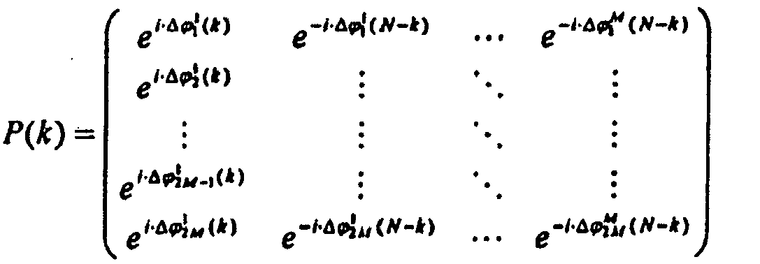 • Δϕm n(k) die Phasendifferenz zwischen dem Signal in dem verzögerten Kanal Nummer n und dem nicht verzögerten Kanal für die eintreffende Frequenz Fm(k) ist, wobei Fm(k) eine Frequenz ist, die zu dem Band Nummer m gehört und die Beziehung
 • Fm(N-k) eine Frequenz ist, die zu dem Band Nummer m gehört und die Beziehung
- System nach einem der vorhergehenden Ansprüche, bei dem die Frequenzdomänentransformation eine Fourier-Transformation ist.
- System nach Anspruch 2, bei dem die Fourier-Transformation die FFT (Schnelle Fourier-Transformation) ist.
- System nach einem der vorhergehenden Ansprüche, bei dem eine inverse Frequenzdomänentransformation auf das komplexe Frequenzdomänen-Ausgangssignal angewendet wird, um ein komplexes Zeitdomänen-Ausgangssignal zu erhalten.
- System nach Anspruch 4, bei dem die inverse Frequenzdomänentransformation die IFFT (inverse FFT) ist.
- System nach einem der vorhergehenden Ansprüche, bei dem das komplexe Frequenzdomänen-Ausgangssignal ein vordefiniertes Frequenzspektrum hat, das wenigstens eine vordefinierte Frequenz umfasst, die ein ganzes Vielfaches und/oder ein halbes Vielfaches einer Abtastfrequenz ist, gemäß der das Analogsignal abgetastet wird.
- System nach Anspruch 1, bei dem M gleich 1 und das Frequenzdomänen-Ausgangssignal ein komplexes Signal ist.
- Verfahren zum Ausführen einer komplexen Abtastung eines Signals, das in eine Frequenzdomäne transformiert wird, mit Hilfe einer 2M-Ordnungs-Abtastung, wobei die Signalbandbreite zu [Fstart, Fstart+MFs] gehört, M eine ganze Zahl ist, Fstart eine Startfrequenz ist, die manuell oder automatisch bestimmt wird, und Fs eine Abtastfrequenz der Abtastung ist und das Verfahren umfassta) Bereitstellen eines Abtastkanals, der dazu eingerichtet ist:a.1. ein Analogsignal in ein entsprechendes im wesentlichen nicht verzögertes Digitalsignal umzuwandeln; unda.2. das Digitalsignal in eine Vielzahl entsprechender im wesentlichen nicht verzögerter diskreter Frequenzdomänenkomponenten umzuwandeln;b) Bereitstellen zusätzlicher 2M-1-Abtastkanäle, die die Ausführung der 2M-Ordnungs-Abtastung ermöglichen, wobei jeder zusätzliche Abtastkanal dazu eingerichtet ist:b.1. ein Analogsignal um einen vorbestimmten Wert zu verzögern, wodurch ein verzögertes Analogsignal erzeugt wird;b.2. das verzögerte Analogsignal in ein entsprechendes verzögertes Digitalsignal umzuwandeln;b.3. das verzögerte Digitalsignal in eine Vielzahl verzögerter diskreter Frequenzdomänenkomponenten umzuwandeln;b.4. wenigstens einen entsprechenden Koeffizienten für jede verzögerte diskrete Frequenzdomänenkomponente und für jedes Ausgabefrequenzband bereitzustellen, das durch [Fstart+(m-1)Fs, Fstart+mFs], m ∈ [1, M], definiert ist; undb.5. den wenigstens einen entsprechenden Koeffizienten mit der jeweiligen entsprechenden verzögerten diskreten Frequenzdomänenkomponente zu multiplizieren, wodurch die multiplizierten verzögerten diskreten Frequenzdomänenkomponenten erzeugt werden; undc) Kombinieren der multiplizierten verzögerten diskreten Frequenzdomänenkomponenten mit den entsprechenden im wesentlichen nicht verzögerten diskreten Frequenzdomänenkomponenten, wodurch ein komplexes Frequenzdomänen-Ausgangssignal erzeugt wird;
wobei- das Frequenzdomänen-Ausgangssignal Ym für ein entsprechendes Ausgabefrequenzband m durch • Xn(k) den diskreten Frequenzdomänenkomponenten aus den Abtastkanälen entspricht;• Qn m(k) = [P-1(k)]n 2m-1 die Koeffizienten für jede verzögerte diskrete Frequenzdomänenkomponente und für jedes Ausgabefrequenzband sind;•
 • Δϕm n(k) die Phasendifferenz zwischen dem Signal in dem verzögerten Kanal Nummer n und dem nicht verzögerten Kanal für die eintreffende Frequenz Fm(k) ist;• Fm(k) eine Frequenz ist, die zu dem Band Nummer m gehört und die Beziehung
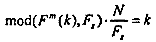 • Fm(N-k) eine Frequenz ist, die zu dem Band Nummer m gehört und die Beziehung
Priority Applications (1)
| Application Number | Priority Date | Filing Date | Title |
|---|---|---|---|
| EP13001606.6A EP2611027A1 (de) | 2010-04-11 | 2011-04-11 | Berechnung von Zeitverzögerungen |
Applications Claiming Priority (1)
| Application Number | Priority Date | Filing Date | Title |
|---|---|---|---|
| IL204983A IL204983A (en) | 2010-04-11 | 2010-04-11 | A method and system for performing signal sampling by using one or more sampling channels and calculating time delays between these channels |
Related Child Applications (1)
| Application Number | Title | Priority Date | Filing Date |
|---|---|---|---|
| EP13001606.6 Division-Into | 2013-03-28 |
Publications (2)
| Publication Number | Publication Date |
|---|---|
| EP2391001A1 EP2391001A1 (de) | 2011-11-30 |
| EP2391001B1 true EP2391001B1 (de) | 2013-06-05 |
Family
ID=43569818
Family Applications (2)
| Application Number | Title | Priority Date | Filing Date |
|---|---|---|---|
| EP11161952.4A Active EP2391001B1 (de) | 2010-04-11 | 2011-04-11 | Einführung einer komplexen Abtastung |
| EP13001606.6A Withdrawn EP2611027A1 (de) | 2010-04-11 | 2011-04-11 | Berechnung von Zeitverzögerungen |
Family Applications After (1)
| Application Number | Title | Priority Date | Filing Date |
|---|---|---|---|
| EP13001606.6A Withdrawn EP2611027A1 (de) | 2010-04-11 | 2011-04-11 | Berechnung von Zeitverzögerungen |
Country Status (6)
| Country | Link |
|---|---|
| EP (2) | EP2391001B1 (de) |
| AU (1) | AU2011241819B2 (de) |
| CL (1) | CL2012002830A1 (de) |
| IL (1) | IL204983A (de) |
| SG (2) | SG191581A1 (de) |
| WO (1) | WO2011128881A2 (de) |
Families Citing this family (3)
| Publication number | Priority date | Publication date | Assignee | Title |
|---|---|---|---|---|
| EP2912639A1 (de) * | 2012-10-25 | 2015-09-02 | MEI, Inc. | System zum klassifizieren von wertgegenständen |
| GB2507349B (en) | 2012-10-29 | 2015-06-10 | Thales Holdings Uk Plc | Sampling device |
| CN113765614B (zh) * | 2021-09-08 | 2023-06-23 | 中国科学院新疆天文台 | 一种提高paf数据处理终端接收信息效率的系统及方法 |
Family Cites Families (3)
| Publication number | Priority date | Publication date | Assignee | Title |
|---|---|---|---|---|
| US5109188A (en) | 1991-03-06 | 1992-04-28 | The United States Of America As Represented By The Secretary Of The Air Force | Instantaneous frequency measurement receiver with bandwidth improvement through phase shifted sampling of real signals |
| US5099243A (en) | 1991-03-06 | 1992-03-24 | The United States Of America As Represented By The Secretary Of The Air Force | Digital frequency measurement receiver with bandwidth improvement through multiple sampling of complex signals |
| US5099194A (en) | 1991-03-06 | 1992-03-24 | The United States Of America As Represented By The Secretary Of The Air Force | Digital frequency measurement receiver with bandwidth improvement through multiple sampling of real signals |
-
2010
- 2010-04-11 IL IL204983A patent/IL204983A/en active IP Right Grant
-
2011
- 2011-04-11 EP EP11161952.4A patent/EP2391001B1/de active Active
- 2011-04-11 EP EP13001606.6A patent/EP2611027A1/de not_active Withdrawn
- 2011-06-09 SG SG2013037460A patent/SG191581A1/en unknown
- 2011-06-09 AU AU2011241819A patent/AU2011241819B2/en not_active Ceased
- 2011-06-09 WO PCT/IB2011/052517 patent/WO2011128881A2/en not_active Ceased
- 2011-06-09 SG SG2012073292A patent/SG184409A1/en unknown
-
2012
- 2012-10-10 CL CL2012002830A patent/CL2012002830A1/es unknown
Also Published As
| Publication number | Publication date |
|---|---|
| CL2012002830A1 (es) | 2013-07-05 |
| EP2391001A1 (de) | 2011-11-30 |
| WO2011128881A3 (en) | 2012-01-05 |
| SG184409A1 (en) | 2012-11-29 |
| EP2611027A1 (de) | 2013-07-03 |
| IL204983A0 (en) | 2010-12-30 |
| WO2011128881A2 (en) | 2011-10-20 |
| AU2011241819B2 (en) | 2015-02-05 |
| AU2011241819A1 (en) | 2012-11-08 |
| SG191581A1 (en) | 2013-07-31 |
| IL204983A (en) | 2015-07-30 |
Similar Documents
| Publication | Publication Date | Title |
|---|---|---|
| US8548100B2 (en) | Method and system for performing complex sampling of signals by using two or more sampling channels and for calculating time delays between these channels | |
| EP2060081B1 (de) | Frequenzabhängige I/Q-Ungleichgewichtsschätzung | |
| US8514979B2 (en) | Integrated demodulator, filter and decimator (DFD) for a radio receiver | |
| US6600438B2 (en) | Broadband IF conversion using two ADCs | |
| US8976914B2 (en) | Multi-tap IQ imbalance estimation and correction circuit and method | |
| TW200308159A (en) | Systems and methods to provide wideband magnitude and phase imbalance calibration and compensation in quadrature receivers | |
| WO2012118543A2 (en) | Method and apparatus for complex in-phase quadrature polyphase nonlinear equalization | |
| EP1356313B1 (de) | Schnelles filter | |
| EP2391001B1 (de) | Einführung einer komplexen Abtastung | |
| Morrison et al. | Performance of oversampled polyphase filterbank inversion via Fourier transform | |
| US7564386B2 (en) | Pre-processing data samples from parallelized data converters | |
| CN105102992A (zh) | 确定delta-sigma调制信号的均方根的方法和装置 | |
| EP0695028B1 (de) | Signalsummiereinrichtung in kleinem Massstab und differentielle Detektionseinrichtung | |
| JP2001045081A (ja) | 信号処理方法 | |
| KR101818656B1 (ko) | 2 이상의 샘플링 채널을 사용하여 신호의 복소 샘플링을 수행하고 이들 채널들 간에 시간지연을 계산하기 위한 방법 및 시스템 | |
| US8615538B1 (en) | Sub-filtering finite impulse response (FIR) filter for frequency search capability | |
| CA2739778A1 (en) | Method and system for performing complex sampling of signals by using two or more sampling channels and for calculating time delays between these channels | |
| AU2011202195A1 (en) | Method and system for performing complex sampling of signals by using two or more sampling channels and for calculating time delays between these channels | |
| Džafić et al. | Computation of Discrete-Time Analytic Signals | |
| US20030007583A1 (en) | Correction of multiple transmission impairments | |
| SG185841A1 (en) | Method and system for performing complex sampling of signals by using two or more sampling channels and for calculating time delays between these channels | |
| CN115575985A (zh) | 一种高效率的导航信号相关峰精细采样计算方法 | |
| Kennedy | Lecture notes on the design of low-pass digital filters with wireless-communication applications | |
| RU209338U1 (ru) | Устройство для демодуляции ofdm-сигнала с децимацией частоты дискретизации | |
| CN121077862A (zh) | 一种利于工程上实现数字信号频偏纠正的方法 |
Legal Events
| Date | Code | Title | Description |
|---|---|---|---|
| AK | Designated contracting states |
Kind code of ref document: A1 Designated state(s): AL AT BE BG CH CY CZ DE DK EE ES FI FR GB GR HR HU IE IS IT LI LT LU LV MC MK MT NL NO PL PT RO RS SE SI SK SM TR |
|
| AX | Request for extension of the european patent |
Extension state: BA ME |
|
| PUAI | Public reference made under article 153(3) epc to a published international application that has entered the european phase |
Free format text: ORIGINAL CODE: 0009012 |
|
| 17P | Request for examination filed |
Effective date: 20120530 |
|
| GRAP | Despatch of communication of intention to grant a patent |
Free format text: ORIGINAL CODE: EPIDOSNIGR1 |
|
| GRAP | Despatch of communication of intention to grant a patent |
Free format text: ORIGINAL CODE: EPIDOSNIGR1 |
|
| GRAJ | Information related to disapproval of communication of intention to grant by the applicant or resumption of examination proceedings by the epo deleted |
Free format text: ORIGINAL CODE: EPIDOSDIGR1 |
|
| GRAP | Despatch of communication of intention to grant a patent |
Free format text: ORIGINAL CODE: EPIDOSNIGR1 |
|
| GRAS | Grant fee paid |
Free format text: ORIGINAL CODE: EPIDOSNIGR3 |
|
| GRAA | (expected) grant |
Free format text: ORIGINAL CODE: 0009210 |
|
| AK | Designated contracting states |
Kind code of ref document: B1 Designated state(s): AL AT BE BG CH CY CZ DE DK EE ES FI FR GB GR HR HU IE IS IT LI LT LU LV MC MK MT NL NO PL PT RO RS SE SI SK SM TR |
|
| REG | Reference to a national code |
Ref country code: GB Ref legal event code: FG4D |
|
| REG | Reference to a national code |
Ref country code: CH Ref legal event code: EP |
|
| REG | Reference to a national code |
Ref country code: AT Ref legal event code: REF Ref document number: 616173 Country of ref document: AT Kind code of ref document: T Effective date: 20130615 |
|
| REG | Reference to a national code |
Ref country code: IE Ref legal event code: FG4D |
|
| REG | Reference to a national code |
Ref country code: DE Ref legal event code: R096 Ref document number: 602011001888 Country of ref document: DE Effective date: 20130801 |
|
| REG | Reference to a national code |
Ref country code: CH Ref legal event code: NV Representative=s name: MARKS AND CLERK (LUXEMBOURG) LLP, CH |
|
| REG | Reference to a national code |
Ref country code: AT Ref legal event code: MK05 Ref document number: 616173 Country of ref document: AT Kind code of ref document: T Effective date: 20130605 |
|
| PG25 | Lapsed in a contracting state [announced via postgrant information from national office to epo] |
Ref country code: SI Free format text: LAPSE BECAUSE OF FAILURE TO SUBMIT A TRANSLATION OF THE DESCRIPTION OR TO PAY THE FEE WITHIN THE PRESCRIBED TIME-LIMIT Effective date: 20130605 Ref country code: AT Free format text: LAPSE BECAUSE OF FAILURE TO SUBMIT A TRANSLATION OF THE DESCRIPTION OR TO PAY THE FEE WITHIN THE PRESCRIBED TIME-LIMIT Effective date: 20130605 Ref country code: GR Free format text: LAPSE BECAUSE OF FAILURE TO SUBMIT A TRANSLATION OF THE DESCRIPTION OR TO PAY THE FEE WITHIN THE PRESCRIBED TIME-LIMIT Effective date: 20130906 Ref country code: SE Free format text: LAPSE BECAUSE OF FAILURE TO SUBMIT A TRANSLATION OF THE DESCRIPTION OR TO PAY THE FEE WITHIN THE PRESCRIBED TIME-LIMIT Effective date: 20130605 Ref country code: ES Free format text: LAPSE BECAUSE OF FAILURE TO SUBMIT A TRANSLATION OF THE DESCRIPTION OR TO PAY THE FEE WITHIN THE PRESCRIBED TIME-LIMIT Effective date: 20130916 Ref country code: LT Free format text: LAPSE BECAUSE OF FAILURE TO SUBMIT A TRANSLATION OF THE DESCRIPTION OR TO PAY THE FEE WITHIN THE PRESCRIBED TIME-LIMIT Effective date: 20130605 Ref country code: NO Free format text: LAPSE BECAUSE OF FAILURE TO SUBMIT A TRANSLATION OF THE DESCRIPTION OR TO PAY THE FEE WITHIN THE PRESCRIBED TIME-LIMIT Effective date: 20130905 |
|
| REG | Reference to a national code |
Ref country code: NL Ref legal event code: VDEP Effective date: 20130605 |
|
| REG | Reference to a national code |
Ref country code: LT Ref legal event code: MG4D |
|
| PG25 | Lapsed in a contracting state [announced via postgrant information from national office to epo] |
Ref country code: HR Free format text: LAPSE BECAUSE OF FAILURE TO SUBMIT A TRANSLATION OF THE DESCRIPTION OR TO PAY THE FEE WITHIN THE PRESCRIBED TIME-LIMIT Effective date: 20130605 Ref country code: RS Free format text: LAPSE BECAUSE OF FAILURE TO SUBMIT A TRANSLATION OF THE DESCRIPTION OR TO PAY THE FEE WITHIN THE PRESCRIBED TIME-LIMIT Effective date: 20130605 Ref country code: BG Free format text: LAPSE BECAUSE OF FAILURE TO SUBMIT A TRANSLATION OF THE DESCRIPTION OR TO PAY THE FEE WITHIN THE PRESCRIBED TIME-LIMIT Effective date: 20130905 |
|
| PG25 | Lapsed in a contracting state [announced via postgrant information from national office to epo] |
Ref country code: LV Free format text: LAPSE BECAUSE OF FAILURE TO SUBMIT A TRANSLATION OF THE DESCRIPTION OR TO PAY THE FEE WITHIN THE PRESCRIBED TIME-LIMIT Effective date: 20130605 |
|
| PG25 | Lapsed in a contracting state [announced via postgrant information from national office to epo] |
Ref country code: SK Free format text: LAPSE BECAUSE OF FAILURE TO SUBMIT A TRANSLATION OF THE DESCRIPTION OR TO PAY THE FEE WITHIN THE PRESCRIBED TIME-LIMIT Effective date: 20130605 Ref country code: IS Free format text: LAPSE BECAUSE OF FAILURE TO SUBMIT A TRANSLATION OF THE DESCRIPTION OR TO PAY THE FEE WITHIN THE PRESCRIBED TIME-LIMIT Effective date: 20131005 Ref country code: BE Free format text: LAPSE BECAUSE OF FAILURE TO SUBMIT A TRANSLATION OF THE DESCRIPTION OR TO PAY THE FEE WITHIN THE PRESCRIBED TIME-LIMIT Effective date: 20130605 Ref country code: PT Free format text: LAPSE BECAUSE OF FAILURE TO SUBMIT A TRANSLATION OF THE DESCRIPTION OR TO PAY THE FEE WITHIN THE PRESCRIBED TIME-LIMIT Effective date: 20131007 Ref country code: EE Free format text: LAPSE BECAUSE OF FAILURE TO SUBMIT A TRANSLATION OF THE DESCRIPTION OR TO PAY THE FEE WITHIN THE PRESCRIBED TIME-LIMIT Effective date: 20130605 |
|
| PG25 | Lapsed in a contracting state [announced via postgrant information from national office to epo] |
Ref country code: RO Free format text: LAPSE BECAUSE OF FAILURE TO SUBMIT A TRANSLATION OF THE DESCRIPTION OR TO PAY THE FEE WITHIN THE PRESCRIBED TIME-LIMIT Effective date: 20130605 Ref country code: PL Free format text: LAPSE BECAUSE OF FAILURE TO SUBMIT A TRANSLATION OF THE DESCRIPTION OR TO PAY THE FEE WITHIN THE PRESCRIBED TIME-LIMIT Effective date: 20130605 Ref country code: NL Free format text: LAPSE BECAUSE OF FAILURE TO SUBMIT A TRANSLATION OF THE DESCRIPTION OR TO PAY THE FEE WITHIN THE PRESCRIBED TIME-LIMIT Effective date: 20130605 |
|
| PLBE | No opposition filed within time limit |
Free format text: ORIGINAL CODE: 0009261 |
|
| STAA | Information on the status of an ep patent application or granted ep patent |
Free format text: STATUS: NO OPPOSITION FILED WITHIN TIME LIMIT |
|
| PG25 | Lapsed in a contracting state [announced via postgrant information from national office to epo] |
Ref country code: DK Free format text: LAPSE BECAUSE OF FAILURE TO SUBMIT A TRANSLATION OF THE DESCRIPTION OR TO PAY THE FEE WITHIN THE PRESCRIBED TIME-LIMIT Effective date: 20130605 |
|
| 26N | No opposition filed |
Effective date: 20140306 |
|
| REG | Reference to a national code |
Ref country code: DE Ref legal event code: R097 Ref document number: 602011001888 Country of ref document: DE Effective date: 20140306 |
|
| PGFP | Annual fee paid to national office [announced via postgrant information from national office to epo] |
Ref country code: FI Payment date: 20140410 Year of fee payment: 4 Ref country code: IT Payment date: 20140430 Year of fee payment: 4 Ref country code: CZ Payment date: 20140408 Year of fee payment: 4 Ref country code: CH Payment date: 20140414 Year of fee payment: 4 |
|
| PG25 | Lapsed in a contracting state [announced via postgrant information from national office to epo] |
Ref country code: MC Free format text: LAPSE BECAUSE OF FAILURE TO SUBMIT A TRANSLATION OF THE DESCRIPTION OR TO PAY THE FEE WITHIN THE PRESCRIBED TIME-LIMIT Effective date: 20130605 Ref country code: LU Free format text: LAPSE BECAUSE OF FAILURE TO SUBMIT A TRANSLATION OF THE DESCRIPTION OR TO PAY THE FEE WITHIN THE PRESCRIBED TIME-LIMIT Effective date: 20140411 |
|
| REG | Reference to a national code |
Ref country code: IE Ref legal event code: MM4A |
|
| PG25 | Lapsed in a contracting state [announced via postgrant information from national office to epo] |
Ref country code: IE Free format text: LAPSE BECAUSE OF NON-PAYMENT OF DUE FEES Effective date: 20140411 |
|
| PG25 | Lapsed in a contracting state [announced via postgrant information from national office to epo] |
Ref country code: CZ Free format text: LAPSE BECAUSE OF NON-PAYMENT OF DUE FEES Effective date: 20150411 |
|
| REG | Reference to a national code |
Ref country code: CH Ref legal event code: PL |
|
| PG25 | Lapsed in a contracting state [announced via postgrant information from national office to epo] |
Ref country code: FI Free format text: LAPSE BECAUSE OF NON-PAYMENT OF DUE FEES Effective date: 20150411 Ref country code: IT Free format text: LAPSE BECAUSE OF NON-PAYMENT OF DUE FEES Effective date: 20150411 Ref country code: LI Free format text: LAPSE BECAUSE OF NON-PAYMENT OF DUE FEES Effective date: 20150430 Ref country code: CH Free format text: LAPSE BECAUSE OF NON-PAYMENT OF DUE FEES Effective date: 20150430 |
|
| PG25 | Lapsed in a contracting state [announced via postgrant information from national office to epo] |
Ref country code: MT Free format text: LAPSE BECAUSE OF FAILURE TO SUBMIT A TRANSLATION OF THE DESCRIPTION OR TO PAY THE FEE WITHIN THE PRESCRIBED TIME-LIMIT Effective date: 20130605 |
|
| REG | Reference to a national code |
Ref country code: FR Ref legal event code: PLFP Year of fee payment: 6 |
|
| PG25 | Lapsed in a contracting state [announced via postgrant information from national office to epo] |
Ref country code: SM Free format text: LAPSE BECAUSE OF FAILURE TO SUBMIT A TRANSLATION OF THE DESCRIPTION OR TO PAY THE FEE WITHIN THE PRESCRIBED TIME-LIMIT Effective date: 20130605 |
|
| PG25 | Lapsed in a contracting state [announced via postgrant information from national office to epo] |
Ref country code: CY Free format text: LAPSE BECAUSE OF FAILURE TO SUBMIT A TRANSLATION OF THE DESCRIPTION OR TO PAY THE FEE WITHIN THE PRESCRIBED TIME-LIMIT Effective date: 20130605 |
|
| PG25 | Lapsed in a contracting state [announced via postgrant information from national office to epo] |
Ref country code: HU Free format text: LAPSE BECAUSE OF FAILURE TO SUBMIT A TRANSLATION OF THE DESCRIPTION OR TO PAY THE FEE WITHIN THE PRESCRIBED TIME-LIMIT; INVALID AB INITIO Effective date: 20110411 Ref country code: TR Free format text: LAPSE BECAUSE OF FAILURE TO SUBMIT A TRANSLATION OF THE DESCRIPTION OR TO PAY THE FEE WITHIN THE PRESCRIBED TIME-LIMIT Effective date: 20130605 |
|
| REG | Reference to a national code |
Ref country code: FR Ref legal event code: PLFP Year of fee payment: 7 |
|
| REG | Reference to a national code |
Ref country code: FR Ref legal event code: PLFP Year of fee payment: 8 |
|
| PG25 | Lapsed in a contracting state [announced via postgrant information from national office to epo] |
Ref country code: MK Free format text: LAPSE BECAUSE OF FAILURE TO SUBMIT A TRANSLATION OF THE DESCRIPTION OR TO PAY THE FEE WITHIN THE PRESCRIBED TIME-LIMIT Effective date: 20130605 |
|
| PG25 | Lapsed in a contracting state [announced via postgrant information from national office to epo] |
Ref country code: AL Free format text: LAPSE BECAUSE OF FAILURE TO SUBMIT A TRANSLATION OF THE DESCRIPTION OR TO PAY THE FEE WITHIN THE PRESCRIBED TIME-LIMIT Effective date: 20130605 |
|
| PGFP | Annual fee paid to national office [announced via postgrant information from national office to epo] |
Ref country code: GB Payment date: 20190523 Year of fee payment: 9 |
|
| GBPC | Gb: european patent ceased through non-payment of renewal fee |
Effective date: 20200411 |
|
| PG25 | Lapsed in a contracting state [announced via postgrant information from national office to epo] |
Ref country code: GB Free format text: LAPSE BECAUSE OF NON-PAYMENT OF DUE FEES Effective date: 20200411 |
|
| PGFP | Annual fee paid to national office [announced via postgrant information from national office to epo] |
Ref country code: FR Payment date: 20250210 Year of fee payment: 15 |
|
| PGFP | Annual fee paid to national office [announced via postgrant information from national office to epo] |
Ref country code: DE Payment date: 20250214 Year of fee payment: 15 |