EP2388858A1 - Antenna device and communication terminal apparatus - Google Patents
Antenna device and communication terminal apparatus Download PDFInfo
- Publication number
- EP2388858A1 EP2388858A1 EP11734686A EP11734686A EP2388858A1 EP 2388858 A1 EP2388858 A1 EP 2388858A1 EP 11734686 A EP11734686 A EP 11734686A EP 11734686 A EP11734686 A EP 11734686A EP 2388858 A1 EP2388858 A1 EP 2388858A1
- Authority
- EP
- European Patent Office
- Prior art keywords
- inductance
- inductance element
- coil
- antenna
- circuit
- Prior art date
- Legal status (The legal status is an assumption and is not a legal conclusion. Google has not performed a legal analysis and makes no representation as to the accuracy of the status listed.)
- Granted
Links
Images














Classifications
-
- H—ELECTRICITY
- H01—ELECTRIC ELEMENTS
- H01Q—ANTENNAS, i.e. RADIO AERIALS
- H01Q1/00—Details of, or arrangements associated with, antennas
- H01Q1/50—Structural association of antennas with earthing switches, lead-in devices or lightning protectors
-
- H—ELECTRICITY
- H01—ELECTRIC ELEMENTS
- H01P—WAVEGUIDES; RESONATORS, LINES, OR OTHER DEVICES OF THE WAVEGUIDE TYPE
- H01P1/00—Auxiliary devices
- H01P1/20—Frequency-selective devices, e.g. filters
- H01P1/201—Filters for transverse electromagnetic waves
- H01P1/203—Strip line filters
- H01P1/20327—Electromagnetic interstage coupling
- H01P1/20336—Comb or interdigital filters
- H01P1/20345—Multilayer filters
-
- H—ELECTRICITY
- H01—ELECTRIC ELEMENTS
- H01P—WAVEGUIDES; RESONATORS, LINES, OR OTHER DEVICES OF THE WAVEGUIDE TYPE
- H01P1/00—Auxiliary devices
- H01P1/20—Frequency-selective devices, e.g. filters
- H01P1/213—Frequency-selective devices, e.g. filters combining or separating two or more different frequencies
- H01P1/2135—Frequency-selective devices, e.g. filters combining or separating two or more different frequencies using strip line filters
-
- H—ELECTRICITY
- H01—ELECTRIC ELEMENTS
- H01P—WAVEGUIDES; RESONATORS, LINES, OR OTHER DEVICES OF THE WAVEGUIDE TYPE
- H01P5/00—Coupling devices of the waveguide type
- H01P5/08—Coupling devices of the waveguide type for linking dissimilar lines or devices
-
- H—ELECTRICITY
- H01—ELECTRIC ELEMENTS
- H01Q—ANTENNAS, i.e. RADIO AERIALS
- H01Q1/00—Details of, or arrangements associated with, antennas
- H01Q1/12—Supports; Mounting means
- H01Q1/22—Supports; Mounting means by structural association with other equipment or articles
- H01Q1/24—Supports; Mounting means by structural association with other equipment or articles with receiving set
-
- H—ELECTRICITY
- H01—ELECTRIC ELEMENTS
- H01Q—ANTENNAS, i.e. RADIO AERIALS
- H01Q13/00—Waveguide horns or mouths; Slot antennas; Leaky-waveguide antennas; Equivalent structures causing radiation along the transmission path of a guided wave
- H01Q13/08—Radiating ends of two-conductor microwave transmission lines, e.g. of coaxial lines, of microstrip lines
-
- H—ELECTRICITY
- H01—ELECTRIC ELEMENTS
- H01Q—ANTENNAS, i.e. RADIO AERIALS
- H01Q5/00—Arrangements for simultaneous operation of antennas on two or more different wavebands, e.g. dual-band or multi-band arrangements
- H01Q5/30—Arrangements for providing operation on different wavebands
- H01Q5/307—Individual or coupled radiating elements, each element being fed in an unspecified way
- H01Q5/314—Individual or coupled radiating elements, each element being fed in an unspecified way using frequency dependent circuits or components, e.g. trap circuits or capacitors
- H01Q5/335—Individual or coupled radiating elements, each element being fed in an unspecified way using frequency dependent circuits or components, e.g. trap circuits or capacitors at the feed, e.g. for impedance matching
-
- H—ELECTRICITY
- H01—ELECTRIC ELEMENTS
- H01Q—ANTENNAS, i.e. RADIO AERIALS
- H01Q5/00—Arrangements for simultaneous operation of antennas on two or more different wavebands, e.g. dual-band or multi-band arrangements
- H01Q5/30—Arrangements for providing operation on different wavebands
- H01Q5/307—Individual or coupled radiating elements, each element being fed in an unspecified way
- H01Q5/342—Individual or coupled radiating elements, each element being fed in an unspecified way for different propagation modes
- H01Q5/357—Individual or coupled radiating elements, each element being fed in an unspecified way for different propagation modes using a single feed point
- H01Q5/364—Creating multiple current paths
-
- H—ELECTRICITY
- H01—ELECTRIC ELEMENTS
- H01Q—ANTENNAS, i.e. RADIO AERIALS
- H01Q9/00—Electrically-short antennas having dimensions not more than twice the operating wavelength and consisting of conductive active radiating elements
- H01Q9/04—Resonant antennas
- H01Q9/30—Resonant antennas with feed to end of elongated active element, e.g. unipole
-
- H—ELECTRICITY
- H01—ELECTRIC ELEMENTS
- H01F—MAGNETS; INDUCTANCES; TRANSFORMERS; SELECTION OF MATERIALS FOR THEIR MAGNETIC PROPERTIES
- H01F17/00—Fixed inductances of the signal type
- H01F17/0006—Printed inductances
- H01F17/0013—Printed inductances with stacked layers
Definitions
- the present invention relates to an antenna device and a communication terminal apparatus using the same and particularly to an antenna device that achieves matching in a wide frequency band.
- communication terminal apparatuses such as portable phones, may require compatibility with communication systems, such as a GSM (Global System for Mobile Communication), DCS (Digital Communication System), PCS (Personal Communication Services), and UMTS (Universal Mobile Telecommunications System), as well as a GPS (Global Positioning System), a wireless LAN, Bluetooth (registered trademark), and so on.
- GSM Global System for Mobile Communication
- DCS Digital Communication System
- PCS Personal Communication Services
- UMTS Universal Mobile Telecommunications System
- GPS Global Positioning System
- wireless LAN wireless LAN
- Bluetooth registered trademark
- the antenna devices for a wide frequency band typically have a wideband matching circuit includes an LC parallel resonant circuit or an LC series resonant circuit, as disclosed in Patent Document 1 and Patent Document 2. Also, known examples of the antenna devices for a wide frequency band include tunable antennas as disclosed in Patent Document 3 and Patent Document 4.
- the present invention has been made in view of the foregoing situation, and an object of the present invention is to provide an antenna device that achieves impedance matching with a power-supply circuit in a wide frequency band and a communication terminal apparatus having the antenna device.
- An antenna device of the present invention includes an antenna element and an impedance converting circuit connected to the antenna element, wherein the impedance converting circuit includes a first inductance element (L1) and a second inductance element (L2) tightly coupled to the first inductance element, and a pseudo or an equivalent negative inductance component is generated as a result of the tight coupling between the first inductance element and the second inductance element and the negative inductance component suppresses or cancels an effective inductance component of the antenna element.
- the impedance converting circuit includes a first inductance element (L1) and a second inductance element (L2) tightly coupled to the first inductance element, and a pseudo or an equivalent negative inductance component is generated as a result of the tight coupling between the first inductance element and the second inductance element and the negative inductance component suppresses or cancels an effective inductance component of the antenna element.
- the impedance converting circuit includes a transformer-type circuit in which the first inductance element and the second inductance element are tightly coupled to each other via a mutual inductance, and when the transformer-type circuit is equivalently transformed into a T-type circuit constituted by a first port connected to a power-supply circuit, a second port connected to the antenna element, a third port connected to ground, a first inductance element connected between the first port and a branch point, a second inductance element connected between the second port and the branch point, and a third inductance element connected between the third port and the branch point, the pseudo negative inductance component corresponds to the second inductor.
- a first end of the first inductance element is connected to the power-supply circuit, a second end of the first inductance element is connected to ground, a first end of the second inductance element is connected to the antenna element, and a second end of the second inductance element is connected to ground.
- a first end of the first inductance element is connected to the power-supply circuit, a second end of the first inductance element is connected to the antenna element, a first end of the second inductance element is connected to the antenna element, and a second end of the second inductance element is connected to ground.
- the first inductance element (L1) includes a first coil element (L1a) and a second coil element (L1b), the first coil element and the second coil element are interconnected in series, and conductor winding patterns are formed so as to form a closed magnetic path.
- the second inductance element (L2) includes a third coil element (L2a) and a fourth coil element (L2b), the third coil element and the fourth coil element are interconnected in series, and conductor winding patterns are formed so as to form a closed magnetic path.
- the first inductance element and the second inductance element couple to each other via a magnetic field and an electric field; and when an alternating current flows in the first inductance element, a direction of a current flowing in the second inductance element as a result of the coupling via the magnetic field and a direction of a current flowing in the second inductance element as a result of the coupling via the electric field are the same.
- a direction of a current flowing in the second inductance element is a direction in which a magnetic wall is generated between the first inductance element and the second inductance element.
- the first inductance element and the second inductance element are configured with conductor patterns disposed in a laminate (a multilayer substrate) in which multiple dielectric layers or magnetic layers are laminated and the first inductance element and the second inductance element couple to each other inside the laminate.
- the first inductance element is constituted by at least two inductance elements connected electrically in parallel, and the two inductance elements are disposed to have such a positional relationship that the two inductance elements sandwich the second inductance element.
- the second inductance element is constituted by at least two inductance elements connected electrically in parallel, and the two inductance elements are disposed to have such a positional relationship that the two inductance elements sandwich the first inductance element.
- a communication terminal apparatus of the present invention has an antenna device including an antenna element, a power-supply circuit, and an impedance converting circuit connected between the antenna element and the power-supply circuit, wherein the impedance converting circuit includes a first inductance element and a second inductance element tightly coupled to the first inductance element, and a pseudo or an equivalent negative inductance component is generated as a result of the tight coupling between the first inductance element and the second inductance element and the negative inductance component suppresses or cancels an effective inductance component of the antenna element.
- the impedance converting circuit since the impedance converting circuit generates a pseudo negative inductance component and the negative inductance component suppresses an effective inductance component of the antenna element, that is, an apparent inductance component of the antenna element is reduced. As a result, the impedance frequency characteristic of the antenna device becomes small. Accordingly, it is possible to suppress impedance changes in the antenna device over a wide band and it is possible to achieve impedance matching with a power-supply circuit over a wide frequency band.
- the communication apparatus of the present invention has the antenna device and thus can be compatible with various communication systems having different frequency bands.
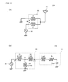
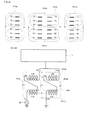
- Fig. 1(A) is a circuit diagram of an antenna device 101 of a first embodiment and Fig. 1(B) is an equivalent circuit diagram thereof.
- the antenna device 101 includes an antenna element 11 and an impedance converting circuit 45 connected to the antenna element 11.
- the antenna element 11 is a monopole antenna.
- the impedance converting circuit 45 is connected to a power-supply end of the antenna element 11.
- the impedance converting circuit 45 is interposed between the antenna element 11 and a power-supply circuit 30.
- the power-supply circuit 30 is a power-supply circuit for supplying high-frequency signals to the antenna element 11, and generates or processes the high-frequency signals.
- the power-supply circuit 30 may also include a circuit for combining or separating the high-frequency signals.
- the impedance converting circuit 45 includes a first inductance element L1 connected to the power-supply circuit 30 and a second inductance element L2 coupled to the first inductance element L1. More specifically, a first end and a second end of the first inductance element L1 are connected to the power-supply circuit 30 and ground, respectively, and a first end and a second of the second inductance element L2 are connected to the first antenna element 11 and ground, respectively.
- the first inductance element L1 and the second inductance element L2 are tightly coupled to each other.
- a negative inductance component is generated in a pseudo manner.
- the negative inductance component cancels an inductance component of the antenna element 11 itself, so that the inductance component of the antenna element 11 is small in appearance. That is, since the effective inductive reactance component of the antenna element 11 is reduced, the antenna element 11 is less likely to be dependent on the frequency of the high-frequency signals.
- the impedance converting circuit 45 includes a transformer-type circuit in which the first inductance element L1 and the second inductance element L2 are tightly coupled to each other via a mutual inductance M.
- the transformer-type circuit can be equivalently transformed into a T-type circuit constituted by three inductance elements Z1, Z2, and Z3, as shown in Fig. 1(B) .
- the T-type circuit includes a first port P1 connected to the power-supply circuit, a second port P2 connected to the antenna element 11, a third port P3 connected to ground, a first inductance element Z1 connected between the first port P1 and a branch point, a second inductance element Z2 connected between the second port P2 and the branch point A, and a third inductance element Z3 connected between the third port P3 and the branch point A.
- the inductance of the first inductance element L1 shown in Fig. 1(A) is indicated by L1
- the inductance of the second inductance element L2 is indicated by L2
- the mutual inductance is indicated by M.
- the inductance of the first inductance element Z1 in Fig. 1(B) is L1-M
- the inductance of the second inductance element Z2 is L2-M
- the inductance of the third inductance element Z3 is +M.
- the inductance of the second inductance element Z2 has a negative value. That is, a pseudo negative composite inductance component is generated in this case.
- the antenna element 11 is equivalently constituted by an inductance component LANT, a radiation resistance component Rr, and a capacitance component CANT.
- the inductance component LANT of the antenna element 11 alone acts so that it is canceled by the negative composite inductance component (L2-M) in the impedance converting circuit 45. That is, the inductance component (of the antenna element 11 including the second inductance element Z2), when the antenna element 11 side is viewed from the point A in the impedance converting circuit is reduced (ideally, to zero), and consequently, the impedance frequency characteristic of the antenna device 101 becomes small.
- the ratio of the impedance transformation performed by the transformer-type circuit is the ratio of the inductance L2 of the second inductance element L2 to the inductance L1 of the first inductance element L1 (L1:L2).
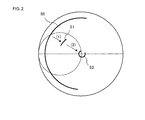
- Fig. 2 is a chart schematically showing an effect of the negative inductance component generated in the impedance converting circuit 45 in a pseudo manner and an effect of the impedance converting circuit 45.
- a curve S0 in Fig. 2 represents, on a Smith chart, an impedance trace obtained by sweeping the frequency over a frequency band used by the antenna element 11. Since the inductance component LANT in the antenna element 11 alone is relatively large, the impedance changes greatly as shown in Fig. 2 .
- a curve S1 in Fig. 2 represents the trace of an impedance when the antenna element 11 side is viewed from the point A in the impedance converting circuit.
- the pseudo negative inductance component in the impedance converting circuit cancels the inductance component LANT of the antenna element, so that the trace of the impedance when the antenna element side is viewed from the point A is reduced significantly.
- a curve S2 in Fig. 2 represents the trace of an impedance viewed from the power-supply circuit 30, i.e., an impedance of the antenna device 101.
- the impedance of the antenna device 101 approaches 50 ⁇ (the center of the Smith chart).
- the impedance may be finely adjusted by adding an inductance element and/or a capacitance element to the transformer-type circuit.
- impedance changes in the antenna device can be suppressed over a wide band. Accordingly, impedance matching with the power-supply circuit is achieved over a wide frequency band.
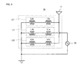
- Fig. 3(A) is a circuit diagram of an antenna device 102 of a second embodiment and Fig. 3(B) is a diagram showing a specific arrangement of coil elements therein.
- the basic configuration of the second embodiment is similar to the configuration of the first embodiment, Figs. 3(A) and 3(B) show a more specific configuration for causing a first inductance element and a second inductance element to couple to each other at a significantly high degree of coupling (to couple tightly).
- a first inductance element L1 includes a first coil element L1a and a second coil element L1b, which are interconnected in series and are wound so as to form a closed magnetic path.
- a second inductance element L2 includes a third coil element L2a and a fourth coil element L2b, which are interconnected in series and are wound so as to form a closed magnetic path.
- the first coil element L1a and the second coil element L1b couple to each other in an opposite phase (additive polarity coupling) and the third coil element L2a and the fourth coil element L2b couple to each other in an opposite phase (additive polarity coupling).
- first coil element L1a and the third coil element L2a couple to each other in the same phase (subtractive polarity coupling) and the second coil element L1b and the fourth coil element L2b couple to each other in the same phase (subtractive polarity coupling).
- Fig. 4 is a diagram in which various arrows indicating the states of magnetic-field coupling and electric-field coupling are written in the circuit shown in Fig. 3(B) .
- a current when a current is supplied from the power-supply circuit in a direction indicated by arrow a in the figure, a current flows in the first coil element L1a in a direction indicated by arrow b in the figure and also a current flows in the second coil element L1b in a direction indicated by arrow c in the figure.
- Those currents form a magnetic flux passing through a closed magnetic path, as indicated by arrow A in the figure.
- the coil element L1a and the coil element L2a also couple to each other via an electric field.
- the coil element L1b and the coil element L2b couple to each other via an electric field. Accordingly, when alternating-current signals flow in the coil element L1a and the coil element L1b, the electric-field couplings cause currents to be excited in the coil element L2a and the coil element L2b.
- Capacitors Ca and Cb in Fig. 4 are symbols presentationally indicating coupling capacitances for the electric-field couplings.
- the first inductance element L1 and the second inductance element L2 couple to each other strongly via both the magnetic field and the electric field. That is, it is possible to reduce the amount of loss and it is possible to transmit a high-frequency energy.
- the impedance converting circuit 35 can be regarded as a circuit configured so that, when an alternating current flows in the first inductance element L1, the direction of a current flowing in the second inductance element L2 as a result of coupling via a magnetic field and the direction of a current flowing in the second inductance element L2 as a result of coupling via an electric field are the same.
- Fig. 5 is a circuit diagram of a multiband-capable antenna device 102.
- This antenna device 102 is for use in a multiband-capable mobile wireless communication system (a 800 MHz band, 900 MHz band, 1800 MHz band, and 1900 MHz band) that is compatible with a GSM system or a CDMA system.
- An antenna element 11 is a branched monopole antenna.
- An impedance converting circuit 35' used in this case has a structure in which a capacitor C1 is interposed between a first inductance element L1 constituted by a coil element L1a and a coil element L1b and a second inductance element L2 constituted by a coil element L2a and a coil element L2b, and other configurations are similar to those of the above-described impedance converting circuit 35.
- This antenna device 102 is utilized as a main antenna for a communication terminal apparatus.
- a first radiation unit of the branched monopole antenna element 11 acts mainly as an antenna radiation element for a high band side (a band of 1800 to 2400 MHz) and the first radiation unit and a second radiation unit together act mainly as an antenna element for a low band side (a band of 800 to 900 MHz).
- the branched monopole antenna element 11 does not necessarily have to resonate at the respective corresponding frequency bands. This is because the impedance converting circuit 35' causes the characteristic impedance of each radiation unit to match the impedance of a power-supply circuit 30.
- the impedance converting circuit 35' causes the characteristic impedance of the second radiation unit to match the impedance (typically, 50 ⁇ ) of the power-supply circuit 30, for example, in the band of 800 to 900 MHz.
- the impedance typically, 50 ⁇
- a high-band high-frequency signals supplied from the power-supply circuit 30 to be radiated from the first radiation unit or it is possible to cause a high-band high-frequency signals received by the first radiation unit to be supplied to the power-supply circuit 30.
- the capacitor C1 in the impedance converting circuit 35' allows passage of particularly high-frequency band signals of high-band high-frequency signals. This can achieve an even wider band of the antenna device. According to the structure of the present embodiment, since the antenna and the power-supply circuit are separated from each other in terms of direct current, the structure is tolerant of ESD.
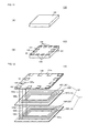
- Fig. 6(A) is a perspective view of an impedance converting circuit 35 of a third embodiment and Fig. 6(B) is a perspective view when the impedance converting circuit 35 is viewed from the lower-surface side.
- Fig. 7 is an exploded perspective view of a laminate 40 that provides the impedance converting circuit 35.
- a conductor pattern 61 is formed at a base layer 51a, which is an uppermost layer of the laminate 40
- a conductor pattern 62 (62a and 62b) is formed at a base layer 51b, which is a second layer
- conductor patterns 63 and 64 are formed at a base layer 51c, which is a third layer.
- Two conductor patterns 65 and 66 are formed at a base layer 51d, which is a fourth layer
- a conductor pattern 67 (67a and 67b) is formed at a base layer 51e, which is a fifth layer.
- a ground conductor 68 is formed at a base layer 51f, which is a sixth layer, and a power-supply terminal 41, a ground terminal 42, and an antenna terminal 43 are formed at the reverse side of a base layer 51g, which is a seventh layer.
- a plain base layer, which is not shown, is stacked on the base layer 51a, which is the uppermost layer.
- the conductor patterns 62a and 63 constitute the first coil element L1a and the conductor patterns 62b and 64 constitute the second coil element L1b.
- the conductor patterns 65 and 67a constitute the third coil element L2a and the conductor patterns 66 and 67b constitute the fourth coil element L2b.
- the various conductor patterns 61 to 68 can be formed using conductive material, such as silver or copper, as a main component.
- conductive material such as silver or copper
- a glass ceramic material, an epoxy resin material, or the like can be used in the case of a dielectric substance and a ferrite ceramic material, a resin material containing ferrite, or the like can be used in the case of a magnetic substance.
- material for the base layers it is preferable to use a dielectric material when an impedance converting circuit for a UHF band is to be formed and it is preferable to use a magnetic material when an impedance converting circuit for an HF band is to be formed.
- the conductor patterns 61 to 68 and the terminals 41, 42, and 43 are connected through corresponding inter-layer connection conductors (via conductors) to provide the circuit shown in Fig. 4 .
- the first coil element L1a and the second coil element L1b are adjacently arranged so that the winding axes of the coil patterns thereof are parallel to each other.
- the third coil element L2a and the fourth coil element L2b are adjacently arranged so that the winding axes of the coil patterns thereof are parallel to each other.
- first coil element L1a and the third coil element L2a are proximately arranged (in a coaxial relationship) so that the winding axes of the coil patterns thereof are along substantially the same straight line.
- second coil element L1b and the fourth coil element L2b are proximately arranged (in a coaxial relationship) so that the winding axes of the coil patterns thereof are along substantially the same straight line. That is, when viewed from the stacking direction of the base layers, the conductor patterns that constitute the coil patterns are arranged so as to overlap each other.
- each of the coil elements L1a, L1b, L2a, and L2b is constituted by a substantially two-turn loop conductor, the number of turns is not limited thereto. Also, the winding axes of the coil patterns of the first coil element L1a and the third coil element L2a do not necessarily have to be arranged so as to be strictly along the same straight line, and may be wound so that coil openings of the first coil element L1a and the third coil element L2a overlap each other in plan view.
- the winding axes of the coil patterns of the second coil element L1b and the fourth coil element L2b do not necessarily have to be arranged so as to be strictly along the same straight line, and may be wound so that coil openings of the second coil element L1b and the fourth coil element L2b overlap each other in plan view.
- the coil elements L1a, L1b, L2a, and L2b are incorporated and integrated into the laminate 40 made of a dielectric substance or magnetic substance, particularly, the areas that serve as coupling portions between the first inductance element L1 constituted by the coil elements L1a and L1b and the second inductance element L2 constituted by the coil elements L2a and L2b are provided inside the laminate 40.
- the element values of the elements constituting the impedance converting circuit 35 and also the degree of coupling between the first inductance element L1 and the second inductance element L2 become less susceptible to an influence from another electronic element disposed adjacent to the laminate 40. As a result, the frequency characteristics can be further stabilized.
- Fig. 8 is a view showing an operation principle of the impedance converting circuit 35.
- the currents are introduced into the first coil element L1a (the conductor patterns 62a and 63), as indicated by arrows c and d, and are further introduced into the second coil element L1b (the conductor patterns 62b and 64), as indicated by arrows e and f.
- the first coil element L1a (the conductor patterns 62a and 63) and the third coil element L2a (the conductor patterns 65 and 67a) lie parallel to each other, mutual inductive coupling and electric-field coupling cause high-frequency signal currents indicated by arrows g and h to be induced in the third coil element L2a (the conductor patterns 65 and 67a).
- a high-frequency signal current indicated by arrow k flows through the antenna terminal 43 and a high-frequency signal current indicated by arrow 1 flows through the ground terminal 42.
- the current (arrow a) that flows through the power-supply terminal 41 is in an opposite direction, the directions of the other currents are also reversed.
- the first coil element L1a and the second coil element L1b couple to each other in the same phase and the third coil element L2a and the fourth coil element L2b couple to each other in the same phase to form respective closed magnetic paths.
- the two magnetic fluxes C and D are trapped, so that the amount of energy loss between the first coil element L1a and the second coil element L1b and the amount of energy loss between the third coil element L2a and the fourth coil element L2b can be reduced.
- the inductance values of the first coil element L1a and the second coil element L1b and the inductance values of the third coil element L2a and the fourth coil element L2b are set to have substantially the same element value, a leakage magnetic field of the closed magnetic paths is reduced and the energy loss can be further reduced.
- the impedance transformation ratio can be controlled through appropriate design of the element values of the coil elements.
- capacitors Cag and Cbg cause electric-field coupling between the third coil element L2a and the fourth coil element L2b via the ground conductor 68, currents flowing as a result of the electric-field coupling further increase the degree of coupling between the coil elements L2a and L2b. If ground is also present at the upper side, the degree of coupling between the first coil element L1a and the second coil element L1b can also be increased by causing the capacitors Cag and Cbg to generate electric-field coupling between the coil elements L1a and L1b.
- the magnetic flux C excited by a primary current flowing in the first inductance element L1 and the magnetic flux D excited by a secondary current flowing in the second inductance element L2 are generated so that induced currents cause the magnetic fluxes to repulse each other (to repel each other).
- the magnetic field generated in the first coil element L1a and the second coil element L1b and the magnetic field generated in the third coil element L2a and the fourth coil element L2b are trapped in the respective small spaces.
- the first coil element L1a and the third coil element L2a and the second coil element L1b and the fourth coil element L2b couple to each other at higher degrees of coupling. That is, the first inductance element L1 and the second inductance element L2 couple to each other at a high degree of coupling.
- Fig. 9 is a circuit diagram of an antenna device of a fourth embodiment.
- An impedance converting circuit 34 used in this case has a first inductance element L1 and two second inductance elements L21 and L22.
- the second inductance element L22 is constituted by a fifth coil element L2c and a sixth coil element L2d, which couple to each other in the same phase.
- the fifth coil element L2c couples to a first coil element L1a in an opposite phase and the sixth coil element L2d couples to a second coil element L1b in an opposite phase.
- One end of the fifth coil element L2c is connected to a radiation element 11 and one end of the sixth coil element L2d is connected to ground.
- Fig. 10 is an exploded perspective view of a laminate 40 that provides the impedance converting circuit 34.
- This example is an example in which base layers 51i and 51j in which conductors 71, 72, and 73 constituting the fifth coil element L2c and the sixth coil element L2d are formed are further stacked on the laminate 40 shown in Fig. 7 in the third embodiment. That is, the fifth and sixth coil elements are constituted as in the first to fourth coil elements described above, the fifth and sixth coil elements L2c and L2d are constituted by conductors having coil patterns, and the fifth and sixth coil elements L2c and L2d are wound so that magnetic fluxes generated in the fifth and sixth coil elements L2c and L2d form closed magnetic paths.
- the operation principle of the impedance converting circuit 34 of the fourth embodiment is essentially similar to the operation principle of the first to third embodiments described above.
- the first inductance element L1 is disposed so that it is sandwiched by two second inductance elements L21 and L22, to thereby suppress stray capacitance generated between the first inductance element L1 and ground.
- the radiation efficiency of the antenna can be enhanced.
- the first inductance element L1 and the second inductance elements L21 and L22 are more tightly coupled, that is, the leakage magmatic field is reduced, so that the energy transmission loss of high-frequency signals between the first inductance element L1 and the second inductance elements L21 and L22 is reduced.
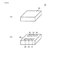
- Fig. 11(A) is a perspective view of an impedance converting circuit 135 of a fifth embodiment and Fig. 11(B) is a perspective view when the impedance converting circuit 135 is viewed from the lower-surface side.
- Fig. 12 is an exploded perspective view of a laminate 40 that provides the impedance converting circuit 135.
- This laminate 140 is one obtained by laminating multiple base layers made of a dielectric substance or magnetic substance.
- the reverse side of the laminate 140 is provided with a power-supply terminal 141 connected to a power-supply circuit 30, a ground terminal 142 connected to ground, and an antenna terminal 143 connected to an antenna element 11.
- the reverse side of the laminate 140 is also provided with NC terminals 144 used for mounting.
- the obverse side of the laminate 140 may also be provided with an inductor and/or a capacitor for impedance matching, as needed.
- An electrode pattern may also be used to form an inductor and/or a capacitor in the laminate 140.
- the various terminals 141, 142, 143, and 144 are formed at a base layer 151a, which is a first layer
- conductor patterns 161 and 163 that serve as first and third coil elements L1a and L2a are formed at a base layer 151b, which is a second layer
- conductor patterns 162 and 164 that serve as second and fourth coil elements L1b and L2b are formed at a base layer 151c, which is a third layer.
- the conductor patterns 161 to 164 can be formed by screen printing using a paste containing conductive material, such as silver or copper, as a main component, metallic-foil etching, or the like.
- a paste containing conductive material such as silver or copper, as a main component, metallic-foil etching, or the like.
- a glass ceramic material, an epoxy resin material, or the like can be used in the case of a dielectric substance and a ferrite ceramic material, a resin material containing ferrite, or the like can be used in the case of a magnetic substance.
- the conductor patterns 161 to 164 and the terminals 141, 142, and 143 are connected to each other through corresponding inter-layer connection conductors (via conductors) to provide the equivalent circuit described above and shown in Fig. 3(A) . That is, the power-supply terminal 141 is connected to one end of the conductor pattern 161 (the first coil element L1a) through a via-hole conductor pattern 165a and another end of the conductor pattern 161 is connected to one end of the conductor pattern 162 (the second coil element L1b) through a via-hole conductor 165b.
- Another end of the conductor pattern 162 is connected to the ground terminal 142 through a via-hole conductor 165c and another end of the branched conductor pattern 164 (the fourth coil element L2b) is connected to one end of the conductor pattern 163 (the third coil element L2a) through a via-hole conductor 165d.
- Another end of the conductor pattern 163 is connected to the antenna terminal 143 through a via-hole conductor pattern 165e.
- the coil elements L1a, L1b, L2a, and L2b are incorporated into the laminate 140 made of a dielectric substance or magnetic substance, particularly, the areas that serve as coupling portions between the first inductance element L1 and the second inductance element L2 are provided inside the laminate 140, as described above, so that the impedance converting circuit 135 becomes less susceptible to an influence from another circuit or element disposed adjacent to the laminate 140. As a result, the frequency characteristics can be further stabilized.
- the first coil element L1a and the third coil element L2a are provided at the same layer (the base layer 151b) in the laminate 140 and the second coil element L1b and the fourth coil element L2b are provided at the same layer (the base layer 151c) in the laminate 140, so that the thickness of the laminate 140 (the impedance converting circuit 135) is reduced.
- the first coil element L1a and the third coil element L2a, which couple to each other, and the second coil element L1b and the fourth coil element L2b, which couple to each other can be formed in the corresponding same processes (e.g., conductive-paste application), so that degree-of-coupling variations due to stack displacement or the like are suppressed and the reliability improves.
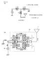
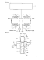
- Fig. 13 is a circuit diagram of an antenna device 106 of a sixth embodiment and Fig. 13(B) is an equivalent circuit diagram thereof.
- the antenna device 106 includes an antenna element 11 and an impedance converting circuit 25 connected to the antenna element 11.
- the antenna element 11 is a monopole antenna.
- the impedance converting circuit 25 is connected to a power-supply end of the antenna element 11.
- the impedance converting circuit 25 (strictly speaking, a first inductance element L1 in the impedance converting circuit 25) is interposed between the antenna element 11 and the power-supply circuit 30.
- the power-supply circuit 30 is a power-supply circuit for supplying high-frequency signals to the antenna element 11 and generates or processes the high-frequency signals.
- the power-supply circuit 30 may also include a circuit for combining or separating the high-frequency signals.
- the impedance converting circuit 25 includes the first inductance element L1 connected to the power-supply circuit 30 and a second inductance element L2 coupled to the first inductance element L1. More specifically, a first end and a second end of the first inductance element L1 are connected to the power-supply circuit 30 and an antenna, respectively, and a first end and a second end of the second inductance element L2 are connected to the antenna element 11 and ground, respectively.
- the first inductance element L1 and the second inductance element L2 are tightly coupled to each other.
- a negative inductance component is generated in a pseudo manner.
- the negative inductance component cancels the inductance component of the antenna element 11 itself, so that the inductance component of the antenna element 11 is reduced in appearance. That is, since the effective inductive reactance component of the antenna element 11 is reduced, the antenna element 11 is less likely to be dependent on the frequency of the high-frequency signals.
- the impedance converting circuit 25 includes a transformer-type circuit in which the first inductance element L1 and the second inductance element L2 are tightly coupled to each other via a mutual inductance M.
- the transformer-type circuit can be equivalently transformed into a T-type circuit constituted by three inductance elements Z1, Z2, and Z3, as shown in Fig. 13(B) .
- this T-type circuit includes a first port P1 connected to the power-supply circuit, a second port P2 connected to the antenna element 11, a third port P3 connected to ground, a first inductance element Z1 connected between the first port P1 and a branch point A, a second inductance element Z2 connected between the second port P2 and the branch point A, and a third inductance element Z3 connected between the third port P3 and the branch point A.
- the inductance of the first inductance element L1 shown in Fig. 13(A) is indicated by L1
- the inductance of the second inductance element L2 is indicated by L2
- the mutual inductance is indicated by M.
- the inductance of the first inductance element Z1 in Fig. 13(B) is L1+M
- the inductance of the second inductance element Z2 is -M
- the inductance of the third inductance element Z3 is L2+M. That is, the inductance of the second inductance element Z2 has a negative value, regardless of the values of L1 and L2. That is, a pseudo negative inductance component is generated in this case.
- the antenna element 11 is equivalently constituted by an inductance component LANT, a radiation resistance component Rr, and a capacitance component CANT.
- the inductance component LANT of the antenna element 11 alone acts so that it is canceled by the negative inductance component (-M) in the impedance converting circuit 45. That is, the inductance component (of the antenna element 11 including the second inductance element Z2), when the antenna element 11 side is viewed from the point A in the impedance converting circuit is reduced (ideally, to zero), and consequently, the impedance frequency characteristic of the antenna device 106 becomes small.
- the degree of coupling be 0.5 or more or, further, 0.7 or more, though depending on the element values of the inductance elements. That is, with such a configuration, a significantly high degree of coupling, such as the degree of coupling in the first embodiment, is not necessarily required.
- Fig. 14(A) is a circuit diagram of an antenna device 107 of a seventh embodiment and Fig. 14(B) is a diagram showing a specific arrangement of coil elements therein.
- the basic configuration of the seventh embodiment is similar to the configuration of the sixth embodiment, Figs. 14(A) and 14(B) show a more specific configuration for causing the first inductance element and the second inductance element to couple to each other at a significantly high degree of coupling (to couple tightly).
- the first inductance element L1 includes a first coil element L1a and a second coil element L1b, which are interconnected in series and are wound so as to form a closed magnetic path.
- the second inductance element L2 also includes a third coil element L2a and a fourth coil element L2b, which are interconnected in series and are wound so as to form a closed magnetic path.
- the first coil element L1a and the second coil element L1b couple to each other in an opposite phase (additive polarity coupling) and the third coil element L2a and the fourth coil element L2b couple to each other in an opposite phase (additive polarity coupling).
- first coil element L1a and the third coil element L2a couple to each other in the same phase (subtractive polarity coupling) and the second coil element L1b and the fourth coil element L2b couple to each other in the same phase (subtractive polarity coupling).
- Fig. 15(A) is a diagram showing the transformation ratio of an impedance converting circuit, the diagram being based on the equivalent circuit shown in Fig. 14(B) .
- Fig. 15(B) is a diagram in which various arrows indicating the states of magnetic-field coupling and electric-field coupling are written in the circuit shown in Fig. 14(B) .
- a current flows in the first coil element L1a in a direction indicated by arrow b in the figure and also a current flows in the coil element L1b in a direction indicated by arrow c in the figure.
- Those currents form a magnetic flux (passing through a closed magnetic path) indicated by arrow A in the figure.
- the coil element L1a and the coil element L2a also couple to each other via an electric field.
- the coil element L1b and the coil element L2b also couple to each other via an electric field. Accordingly, when alternating-current signals flow in the coil element L1a and the coil element L1b, the electric-field couplings cause currents to be excited in the coil element L2a and the coil element L2b.
- Capacitors Ca and Cb in Fig. 4 are symbols presentationally indicating coupling capacitances for the electric-field couplings.
- the first inductance element L1 and the second inductance element L2 strongly couple to each other via both the magnetic field and the electric field.
- the impedance converting circuit 25 can be regarded as a circuit configured so that, when an alternating current flows in the first inductance element L1, the direction of a current flowing in the second inductance element L2 as a result of coupling via a magnetic field and the direction of a current flowing in the second inductance element L2 as a result of coupling via an electric field are the same.
- Fig. 16 is a circuit diagram of a multiband-capable antenna device 107.
- This antenna device 107 is for use in a multiband-capable mobile wireless communication system (a 800 MHz band, 900 MHz band, 1800 MHz band, and 1900 MHz band) that is compatible with a GSM system or a CDMA system.
- a antenna element 11 is a branched monopole antenna.
- This antenna device 102 is utilized as a main antenna for a communication terminal apparatus.
- a first radiation unit of the branched monopole antenna element 11 acts mainly as an antenna radiation element for a high band side (a band of 1800 to 2400 MHz) and the first radiation unit and a second radiation unit together act mainly as an antenna element for a low band side (a band of 800 to 900 MHz).
- the branched monopole antenna element 11 does not necessarily have to resonate at the individual corresponding frequency bands. This is because an impedance converting circuit 25 causes the characteristic impedance of each radiation unit to match the impedance of a power-supply circuit 30.
- the impedance converting circuit 25 causes the characteristic impedance of the second radiation unit to match the impedance (typically, 50 ⁇ ) of the power-supply circuit 30, for example, in the band of 800 to 900 MHz.
- the impedance typically, 50 ⁇
- high-band high-frequency signals supplied from the power-supply circuit 30 to be radiated from the first radiation unit or it is possible to cause high-band high-frequency signals received by the first radiation unit to be supplied to the power-supply circuit 30.
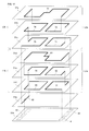
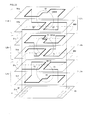
- Fig. 17 is a view showing an example of conductor patterns of individual layers when an impedance converting circuit 25 according to an eighth embodiment is configured in a multilayer substrate.
- the layers are constituted with magnetic sheets.
- the conductor pattern of each layer when in the direction shown in Fig. 17 , is formed at the reverse side of the magnetic sheet, each conductor pattern is indicated by a solid line.
- each linear conductor pattern has a predetermined line width, it is indicated by a simple solid line in this case.
- a conductor pattern 73 is formed in the area indicated in Fig. 17 and at the reverse side of a base layer 51a, conductor patterns 72 and 74 are formed at the reverse side of a base layer 51b, and conductor patterns 71 and 75 are formed at the reverse side of a base layer 51c.
- a conductor pattern 63 is formed at the reverse side of a base layer 51d, conductor patterns 62 and 64 are formed at the reverse side of a base layer 51e, and conductor patterns 61 and 65 are formed at the reverse side of a base layer 51f.
- a conductor pattern 66 is formed at the reverse side of a base layer 51g, and a power-supply terminal 41, a ground terminal 42, and an antenna terminal 43 are formed at the reverse side of a base layer 51h.
- Dotted lines extending vertically in Fig. 17 represent via electrodes, which provide inter-layer connections between the corresponding conductor patterns. Although these via electrodes are, in practice, cylindrical electrodes having predetermined diameter dimensions, they are indicated by simple
- the right half of the conductor pattern 63 and the conductor patterns 61 and 62 constitute a first coil element L1a.
- the left half of the conductor pattern 63 and the conductor patterns 64 and 65 constitute a second coil element L1b.
- the right half of the conductor pattern 73 and the conductor patterns 71 and 72 constitute a third coil element L2a.
- the left half of the conductor pattern 73 and the conductor patterns 74 and 75 constitute a fourth coil element L2b.
- the winding axes of the coil elements L1a, L1b, L2a, and L2b are oriented in the stacking direction of the multiplayer substrate.
- the winding axes of the first coil element L1a and the second coil element L1b are juxtaposed to have a different relationship.
- the third coil element L2a and the fourth coil element L2b are juxtaposed so that the winding axes thereof have a different relationship.
- the winding area of the first coil element L1a and the winding area of the third coil element L2a overlap each other at least partially in plan view and the winding area of the second coil element L1b and the winding area of the fourth coil element L2b overlap each other at least partially in plan view. In this example, they overlap each other substantially completely.
- four coil elements are configured with conductor patterns having an 8-shaped structure.
- Each layer may also be configured with a dielectric sheet.
- a magnetic sheet having a high relative permeability makes it possible to further increase the coefficient of coupling between the coil elements.
- Fig. 18 shows major magnetic fluxes that pass through the coil elements having the conductor patterns formed at the layers of the multiplayer substrate shown in Fig. 17 .
- a magnetic flux FP12 passes through the first coil element L1a constituted by the conductor patterns 61 to 63 and the second coil element L1b constituted by the conductor patterns 63 to 65.
- a magnetic flux FP34 passes through the third coil element L2a constituted by the conductor patterns 71 to 73 and the fourth coil element L2b constituted by the conductor patterns 73 to 75.
- Fig. 19 is a diagram showing a relationship of magnetic couplings of four coil elements L1a, L1b, L2a, and L2b in the impedance converting circuit 25 according to the eighth embodiment.
- the first coil element L1a and the second coil element L1b are wound so that the first coil element L1a and the second coil element L1b constitute a first closed magnetic path (a loop represented by the magnetic flux FP12) and the third coil element L2a and the fourth coil element L2b are wound so that the third coil element L2a and the fourth coil element L2b constitute a second closed magnetic path (a loop represented by the magnetic flux FP34).
- the four coil elements L1a, L1b, L2a, and L2b are wound so that the magnetic flux FP12 passing through the first closed magnetic path and the magnetic flux FP34 passing through the second closed magnetic path are in directions opposite to each other.
- a straight line indicated by a long dashed double-short dashed line in Fig. 19 represents a magnetic wall at which the two magnetic fluxes FP12 and FP34 do not couple to each other. In this manner, the magnetic wall is generated between the coil elements L1a and L2a and between the coil elements L1b and L2b.
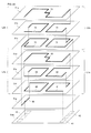
- Fig. 20 is a view showing the configuration of an impedance converting circuit according to a ninth embodiment and showing an example of conductor patterns of individual layers when the impedance converting circuit is configured in a multilayer substrate.
- the conductor pattern of each layer when in the direction shown in Fig. 20 , is formed at the reverse side, each conductor pattern is indicated by a solid line.
- each linear conductor pattern has a predetermined line width, it is indicated by a simple solid line in this case.
- a conductor pattern 73 is formed in the area indicated in Fig. 20 and at the reverse side of a base layer 51a, conductor patterns 72 and 74 are formed at the reverse side of a base layer 51b, and conductor patterns 71 and 75 are formed at the reverse side of a base layer 51c.
- a conductor pattern 63 is formed at the reverse side of a base layer 51d, conductor patterns 62 and 64 are formed at the reverse side of a base layer 51e, and conductor patterns 61 and 65 are formed at the reverse side of a base layer 51f.
- a conductor pattern 66 is formed at the reverse side of a base layer 51g, and a power-supply terminal 41, a ground terminal 42, and an antenna terminal 43 are formed at the reverse side of a base layer 51h.
- Dotted lines extending vertically in Fig. 20 represent via electrodes, which provide inter-layer connections between the corresponding conductor patterns. Although these via electrodes are, in practice, cylindrical electrodes having predetermined diameter dimensions, they are indicated by simple
- the right half of the conductor pattern 63 and the conductor patterns 61 and 62 constitute a first coil element L1a.
- the left half of the conductor pattern 63 and the conductor patterns 64 and 65 constitute a second coil element L1b.
- the right half of the conductor pattern 73 and the conductor patterns 71 and 72 constitute a third coil element L2a.
- the left half of the conductor pattern 73 and the conductor patterns 74 and 75 constitute a fourth coil element L2b.
- Fig. 21 is a diagram showing major magnetic fluxes that pass through the coil elements having the conductor patterns formed at the layers of the multiplayer substrate shown in Fig. 20 .
- Fig. 22 is a diagram showing a relationship of magnetic couplings of four coil elements L1a, L1b, L2a, and L2b in the impedance converting circuit according to the ninth embodiment.
- a magnetic flux FP12 the first coil element L1a and the second coil element L1b constitute a closed magnetic path
- the third coil element L2a and the fourth coil element L2b constitute a closed magnetic path.
- the first coil element L1a and the third coil element L2a constitute a closed magnetic path
- the second coil element L1b and the fourth coil element L2b constitute a closed magnetic path
- the four coil elements L1a, L1b, L2a, and L2b also constitute a closed magnetic path FPall.
- the impedance converting circuit described in the ninth embodiment also offers advantages that are similar to those of the impedance converting circuit 25 in the seventh embodiment.
- Fig. 23 is a view showing an example of conductor patterns of layers in an impedance converting circuit, configured in a multiplayer substrate, according to a tenth embodiment.
- the layers are constituted with magnetic sheets.
- the conductor pattern of each layer when in the direction shown in Fig. 23 , is formed at the reverse side of the magnetic sheet, each conductor pattern is indicated by a solid line.
- each linear conductor pattern has a predetermined line width, it is indicated by a simple solid line in this case.
- a conductor pattern 73 is formed in the area indicated in Fig. 23 and at the reverse side of a base layer 51a, conductor patterns 72 and 74 are formed at the reverse side of a base layer 51b, and conductor patterns 71 and 75 are formed at the reverse side of a base layer 51c.
- Conductor patterns 61 and 65 are formed at the reverse side of a base layer 51d, conductor patterns 62 and 64 are formed at the reverse side of a base layer 51e, and a conductor pattern 63 is formed at the reverse side of a base layer 51f.
- a power-supply terminal 41, a ground terminal 42, and an antenna terminal 43 are formed at the reverse side of a base layer 51g.
- Dotted lines extending vertically in Fig. 23 represent via electrodes, which provide inter-layer connections between the corresponding conductor patterns. Although these via electrodes are, in practice, cylindrical electrodes having predetermined diameter dimensions, they are indicated by simple dotted lines in this case.
- the right half of the conductor pattern 63 and the conductor patterns 61 and 62 constitute a first coil element L1a.
- the left half of the conductor pattern 63 and the conductor patterns 64 and 65 constitute a second coil element L1b.
- the right half of the conductor pattern 73 and the conductor patterns 71 and 72 constitute a third coil element L2a.
- the left half of the conductor pattern 73 and the conductor patterns 74 and 75 constitute a fourth coil element L2b.
- Fig. 24 is a diagram showing a relationship of magnetic couplings of four coil elements L1a, L1b, L2a, and L2b in the impedance converting circuit according to the tenth embodiment.
- the first coil element L1a and the second coil element L1b constitute a first closed magnetic path (a loop represented by a magnetic flux FP12).
- the third coil element L2a and the fourth coil element L2b constitute a second closed magnetic path (a loop represented by a magnetic flux FP34).
- the direction of the magnetic flux FP12 passing through the first closed magnetic path and the direction of the magnetic flux FP34 passing through the second closed magnetic path are opposite to each other.
- the first coil element L1a and the second coil element L1b are referred to as a "primary side” and the third coil element L2a and the fourth coil element L2b are referred to as a "secondary side".
- the power-supply circuit is connected to, in the primary side, a portion that is closer to the secondary side, as shown in Fig. 24 .
- the potential in, in the primary side, the vicinity of the secondary side can be increased, so that the electric-field coupling between the coil element L1a and the coil element L2a increases and the amount of current resulting from the electric-field coupling increases.
- the impedance converting circuit described in the tenth embodiment also offers advantages that are similar to those of the impedance converting circuit 25 in the seventh embodiment.
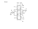
- Fig. 25 is a circuit diagram of an impedance converting circuit according to an eleventh embodiment.
- This impedance converting circuit includes a first series circuit 26 connected between a power-supply circuit 30 and an antenna element 11, a third series circuit 28 connected between the power-supply circuit 30 and the antenna element 11, and a second series circuit 27 connected between the antenna element 11 and ground.
- the first series circuit 26 is a circuit in which a first coil element L1a and a second coil element L1b are connected in series.
- the second series circuit 27 is a circuit in which a third coil element L2a and a fourth coil element L2b are connected in series.
- the third series circuit 28 is a circuit in which a fifth coil element L1c and a sixth coil element L1d are connected in series.
- an enclosure M12 represents coupling between the coil elements L1a and L1b
- an enclosure M34 represents coupling between the coil elements L2a and L2b
- an enclosure M56 represents coupling between the coil elements L1c and L1d.
- An enclosure M135 also represents coupling of the coil elements L1a, L2a, and L1c.
- an enclosure M246 represents coupling of the coil elements L1b, L2b, and L1d.
- the coil elements L2a and L2b constituting a second inductance element is disposed so that they are sandwiched by the coil elements L1a, L1b, L1c, and L1d constituting the first inductance elements, to thereby suppress stray capacitance generated between the second inductance element and ground.
- the radiation efficiency of the antenna can be enhanced.
- Fig. 26 is a view showing an example of conductor patterns of individual layers when the impedance converting circuit according to the eleventh embodiment is configured in a multilayer substrate.
- the layers are constituted with magnetic sheets.
- the conductor pattern of each layer when in the direction shown in Fig. 26 , is formed at the reverse side of the magnetic sheet, each conductor pattern is indicated by a solid line.
- each linear conductor pattern has a predetermined line width, it is indicated by a simple solid line in this case.
- a conductor pattern 82 is formed in the area indicated in Fig. 26 and at the reverse side of a base layer 51a, conductor patterns 81 and 83 are formed at the reverse side of a base layer 51b, and a conductor pattern 72 is formed at the reverse side of a base layer 51c.
- Conductor patterns 71 and 73 are formed at the reverse side of a base layer 51d, conductor patterns 61 and 63 are formed at the reverse side of a base layer 51e, and a conductor pattern 62 is formed at the reverse side of a base layer 51f.
- a power-supply terminal 41, a ground terminal 42, and an antenna terminal 43 are formed at the reverse side of a base layer 51g.
- Dotted lines extending vertically in Fig. 26 represent via electrodes, which provide inter-layer connections between the corresponding conductor patterns. Although these via electrodes are, in practice, cylindrical electrodes having predetermined diameter dimensions, they are indicated by simple dotted lines in this case.
- the right half of the conductor pattern 62 and the conductor pattern 61 constitute a first coil element L1a.
- the left half of the conductor pattern 62 and the conductor pattern 63 constitute a second coil element L1b.
- the conductor pattern 71 and the right half of the conductor pattern 72 constitute a third coil element L2a.
- the left half of the conductor pattern 72 and the conductor pattern 73 constitute a fourth coil element L2b.
- the conductor pattern 81 and the right half of the conductor pattern 82 constitute a fifth coil element L1c.
- the left half of the conductor pattern 82 and the conductor pattern 83 constitute a sixth coil element L1d.
- ellipses indicated by dotted lines represent closed magnetic paths.
- a closed magnetic path CM12 interlinks with the coil elements L1a and L1b.
- a closed magnetic path CM34 also interlinks with the coil elements L2a and L2b.
- a closed magnetic path CM56 also interlinks with the coil elements L1c and L1d.
- the first coil element L1a and the second coil element L1b constitute the first closed magnetic path CM12
- the third coil element L2a and the fourth coil element L2b constitute the second closed magnetic path CM34
- the fifth coil element L1c and the sixth coil element L1d constitute the third closed magnetic path CM56.
- the two magnetic walls MW trap the magnetic flux of the closed magnetic path constituted by the coil elements L1a and L1b, the magnetic flux of the closed magnetic path constituted by the coil elements L2a and L2b, and the magnetic flux of the closed magnetic path constituted by the coil elements L1c and L1d.
- the impedance converting circuit has a structure in which the second closed magnetic path CM34 is sandwiched by the first closed magnetic path CM12 and the third closed magnetic path CM56 in the layer direction.
- the second closed magnetic path CM34 is sandwiched by two magnetic walls and is sufficiently trapped (the effect of trapping is increased). That is, it is possible to cause the impedance converting circuit to act as a transformer having a sufficiently large coupling coefficient.
- the distance between the closed magnetic paths CM12 and CM34 and the distance between the closed magnetic paths CM34 and CM56 can be increased to some extent.
- the circuit in which the series circuit constituted by the coil elements L1a and L1b and the series circuit constituted by the coil elements L1c and L1d are connected in parallel to each other is referred to as a "primary-side circuit” and the series circuit constituted by the coil elements L2a and L2b is referred to as a "secondary-side circuit".
- the impedance converting circuit has a structure in which the first series circuit 26 constituted by the coil elements L1a and L1b and the third series circuit 28 constituted by the coil elements L1c and L1d are connected in parallel to each other, the inductance component of each LC resonant circuit that defines the frequency of the self-resonant point is reduced.
- Both the capacitance component and the inductance component of each LC resonant circuit that defines the frequency of the self-resonant point are reduced, as described above, so that the frequency of the self-resonant point can be set to a high frequency that is sufficiently far from a frequency band used.
- Fig. 27 is a circuit diagram of an impedance converting circuit according to a twelfth embodiment.
- This impedance converting circuit includes a first series circuit 26 connected between a power-supply circuit 30 and an antenna element 11, a third series circuit 28 connected between the power-supply circuit 30 and the antenna element 11, and a second series circuit 27 connected between the antenna element 11 and ground.
- the first series circuit 26 is a circuit in which a first coil element L1a and a second coil element L1b are connected in series.
- the second series circuit 27 is a circuit in which a third coil element L2a and a fourth coil element L2b are connected in series.
- the third series circuit 28 is a circuit in which a fifth coil element L1c and a sixth coil element L1d are connected in series.
- an enclosure M12 represents coupling between the coil elements L1a and L1b
- an enclosure M34 represents coupling between the coil elements L2a and L2b
- an enclosure M56 represents coupling between the coil elements L1c and L1d.
- An enclosure M135 also represents coupling of the coil elements L1a, L2a, and L1c.
- an enclosure M246 represents coupling of the coil elements L1b, L2b, and L1d.
- Fig. 28 is a view showing an example of conductor patterns of individual layers when the impedance converting circuit according to the twelfth embodiment is configured in a multilayer substrate.
- the layers are constituted with magnetic sheets.
- the conductor pattern of each layer when in the direction shown in Fig. 28 , is formed at the reverse side of the magnetic sheet, each conductor pattern is indicated by a solid line.
- each linear conductor pattern has a predetermined line width, it is indicated by a simple solid line in this case.
- the magnetic flux caused by the coil elements L2a and L2b is absorbed by the magnetic flux caused by the coil elements L1c and L1d.
- the magnetic flux hardly leaks, and consequently, it is possible to cause the impedance converting circuit to act as a transformer having a very large coupling coefficient.
- both the capacitance component and the inductance component of each LC resonant circuit that defines the frequency of the self-resonant point are also reduced, so that the frequency of the self-resonant point can be set to a high frequency that is sufficiently far from a frequency band used.
- Fig. 29 is a circuit diagram of an impedance converting circuit according to the thirteenth embodiment.
- This impedance converting circuit includes a first series circuit 26 connected between a power-supply circuit 30 and an antenna element 11, a third series circuit 28 connected between the power-supply circuit 30 and the antenna element 11, and a second series circuit 27 connected between the antenna element 11 and ground.
- Fig. 30 is a view showing an example of conductor patterns of individual layers when the impedance converting circuit according to the thirteenth embodiment is configured in a multilayer substrate.
- the layers are constituted with magnetic sheets.
- the conductor pattern of each layer when in the direction shown in Fig. 30 , is formed at the reverse side of the magnetic sheet, each conductor pattern is indicated by a solid line.
- each linear conductor pattern has a predetermined line width, it is indicated by a simple solid line in this case.
- the closed magnetic paths CM12, CM34, and CM56 shown in Fig. 30 are generated and also the closed magnetic path CM16 is generated, the magnetic flux caused by the coil elements L1a to L1d hardly leaks. As a result, it is possible to cause the impedance converting circuit to act as a transformer having a large coupling coefficient.
- both the capacitance component and the inductance component of each LC resonant circuit that defines the frequency of the self-resonant point are also reduced, so that the frequency of the self-resonant point can be set to a high frequency that is sufficiently far from a frequency band used.
- Fig. 31(A) is a configuration diagram of a communication terminal apparatus that is a first example of the fourteenth embodiment
- Fig. 31(B) is a configuration diagram of a communication terminal apparatus that is a second example.
- These communication terminal apparatuses are, for example, terminals for receiving high-frequency signals (470 to 770 MHz) in a one-segment partial reception service (commonly called "one seg") for portable phones and mobile terminals.
- a communication terminal apparatus 1 shown in Fig. 31(A) has a first casing 10, which is a cover unit, and a second casing 20, which is a main unit.
- the first casing 10 is coupled to the second casing 20 by using a flip or slide mechanism.
- the first casing 10 is provided with a first radiation element 11 that also functions as a ground plate and the second casing 20 is provided with a second radiation element 21 that also serves as a ground plate.
- the first and second radiation elements 11 and 21 are formed of conductive films including thin films, such as metallic foils, or thick films made of a conductive paste or the like.
- the power-supply circuit 30 has a signal processing circuit, such as an RF circuit or a baseband circuit.
- a first radiation element 11 is provided as an individual antenna.
- Various types of antenna element such as a chip antenna, a sheet-metal antenna, and a coil antenna, can be used as the first radiation element 11.
- a linear conductor provided along the inner periphery or outer periphery of a casing 10 may also be used as the antenna element.
- a second radiation element 21 also functions as a ground plate for a second casing 20.
- Various types of antenna may also be used as the second radiation element 21, as in the first radiation element 11.
- the communication terminal apparatus 2 is a straight-structure terminal, not a flip type or a slide type.
- the second radiation element 21 does not necessarily have to be one that functions sufficiently as a radiator, and the first radiation element 11 may also be one that behaves as the so-called "monopole antenna".
- connection line 33 serves as a connection line for electronic components (not shown) included in the first and second casings 10 and 20.
- the connection line 33 behaves as an inductance element with respect to high-frequency signals, but does not directly affect the antenna performance.
- the impedance converting circuit 35 is provided between the power-supply circuit 30 and the first radiation element 11 to stabilize frequency characteristics of high-frequency signals transmitted from the first and second radiation elements 11 and 21 or high-frequency signals received by the first and second radiation elements 11 and 21. Hence, the frequency characteristics of the high-frequency signals are stabilized without being affected by the shapes of the first radiation element 11 and the second radiation element 21, the shapes of the first casing 10 and the second casing 20, and the state of arrangement of adjacent components.
- the impedances of the first and second radiation elements 11 and 21 are likely to vary depending on the opening/closing state of the first casing 10, which is the cover unit, relative to the second casing 20, which is the main unit.
- the impedance converting circuit 35 makes it possible to stabilize the frequency characteristics of the high-frequency signals. That is, frequency-characteristic adjusting functions, including center-frequency setting, passband-width setting, and impedance-matching setting, that are important matters for antenna design can be accomplished by the impedance converting circuit 35. Thus, with respect to the antenna element itself, it is sufficient to consider, mainly, directivity or a gain, thus facilitating the antenna design.
Landscapes
- Physics & Mathematics (AREA)
- Electromagnetism (AREA)
- Details Of Aerials (AREA)
- Near-Field Transmission Systems (AREA)
- Waveguide Connection Structure (AREA)
- Transceivers (AREA)
Abstract
Description
- The present invention relates to an antenna device and a communication terminal apparatus using the same and particularly to an antenna device that achieves matching in a wide frequency band.
- In recent years, communication terminal apparatuses, such as portable phones, may require compatibility with communication systems, such as a GSM (Global System for Mobile Communication), DCS (Digital Communication System), PCS (Personal Communication Services), and UMTS (Universal Mobile Telecommunications System), as well as a GPS (Global Positioning System), a wireless LAN, Bluetooth (registered trademark), and so on. Thus, antenna devices for such communication terminal apparatuses are required to cover a wide frequency band of 800 MHz to 2.4 GHz.
- The antenna devices for a wide frequency band typically have a wideband matching circuit includes an LC parallel resonant circuit or an LC series resonant circuit, as disclosed in
Patent Document 1 andPatent Document 2. Also, known examples of the antenna devices for a wide frequency band include tunable antennas as disclosed in Patent Document 3 and Patent Document 4. -
- PTL 1: Japanese Unexamined Patent Application Publication No.
2004-336250 - PTL 2: Japanese Unexamined Patent Application Publication No.
2006-173697 - PTL 3: Japanese Unexamined Patent Application Publication No.
2000-124728 - PTL 4: Japanese Unexamined Patent Application Publication No.
2008-035065 - However, since each of the matching circuits disclosed in
Patent Documents - On the other hand, since the tunable antennas disclosed in Patent Documents 3 and 4 require a circuit for controlling a variable capacitance element, that is, a switching circuit for switching the frequency band, the circuit configuration is likely to be complicated. Also, since loss and distortion in the switching circuit are large, there are cases in which a sufficient gain is not obtained.
- The present invention has been made in view of the foregoing situation, and an object of the present invention is to provide an antenna device that achieves impedance matching with a power-supply circuit in a wide frequency band and a communication terminal apparatus having the antenna device.
- (1) An antenna device of the present invention includes an antenna element and an impedance converting circuit connected to the antenna element,
wherein the impedance converting circuit includes a first inductance element (L1) and a second inductance element (L2) tightly coupled to the first inductance element, and
a pseudo or an equivalent negative inductance component is generated as a result of the tight coupling between the first inductance element and the second inductance element and the negative inductance component suppresses or cancels an effective inductance component of the antenna element. - (2) In the antenna device described in the (1), for example, the impedance converting circuit includes a transformer-type circuit in which the first inductance element and the second inductance element are tightly coupled to each other via a mutual inductance,
and when the transformer-type circuit is equivalently transformed into a T-type circuit constituted by a first port connected to a power-supply circuit, a second port connected to the antenna element, a third port connected to ground, a first inductance element connected between the first port and a branch point, a second inductance element connected between the second port and the branch point, and a third inductance element connected between the third port and the branch point, the pseudo negative inductance component corresponds to the second inductor. - (3) In the antenna device described in the (1) or (2), for example, a first end of the first inductance element is connected to the power-supply circuit, a second end of the first inductance element is connected to ground, a first end of the second inductance element is connected to the antenna element, and a second end of the second inductance element is connected to ground.
- (4) Also, in the antenna device described in the (1) or (2), for example, a first end of the first inductance element is connected to the power-supply circuit, a second end of the first inductance element is connected to the antenna element, a first end of the second inductance element is connected to the antenna element, and a second end of the second inductance element is connected to ground.
- (5) In the antenna device described in the (3) or (4), preferably, the first inductance element (L1) includes a first coil element (L1a) and a second coil element (L1b), the first coil element and the second coil element are interconnected in series, and conductor winding patterns are formed so as to form a closed magnetic path.
- (6) In the antenna device described in one of the (3) to (5), preferably, the second inductance element (L2) includes a third coil element (L2a) and a fourth coil element (L2b), the third coil element and the fourth coil element are interconnected in series, and conductor winding patterns are formed so as to form a closed magnetic path.
- (7) In the antenna device described in one of the (1) to (6), preferably, the first inductance element and the second inductance element couple to each other via a magnetic field and an electric field; and
when an alternating current flows in the first inductance element, a direction of a current flowing in the second inductance element as a result of the coupling via the magnetic field and a direction of a current flowing in the second inductance element as a result of the coupling via the electric field are the same. - (8) In the antenna device described in one of the (1) to (7), preferably, when an alternating current flows in the first inductance element, a direction of a current flowing in the second inductance element is a direction in which a magnetic wall is generated between the first inductance element and the second inductance element.
- (9) In the antenna device described in one of the (1) to (8), preferably, the first inductance element and the second inductance element are configured with conductor patterns disposed in a laminate (a multilayer substrate) in which multiple dielectric layers or magnetic layers are laminated and the first inductance element and the second inductance element couple to each other inside the laminate.
- (10) In the antenna device described in one of the (1) to (9), preferably, the first inductance element is constituted by at least two inductance elements connected electrically in parallel, and the two inductance elements are disposed to have such a positional relationship that the two inductance elements sandwich the second inductance element.
- (11) In the antenna device described in one of the (1) to (9), preferably, the second inductance element is constituted by at least two inductance elements connected electrically in parallel, and the two inductance elements are disposed to have such a positional relationship that the two inductance elements sandwich the first inductance element.
- (12) A communication terminal apparatus of the present invention has an antenna device including an antenna element, a power-supply circuit, and an impedance converting circuit connected between the antenna element and the power-supply circuit,
wherein the impedance converting circuit includes a first inductance element and a second inductance element tightly coupled to the first inductance element, and
a pseudo or an equivalent negative inductance component is generated as a result of the tight coupling between the first inductance element and the second inductance element and the negative inductance component suppresses or cancels an effective inductance component of the antenna element. Advantageous Effects of Invention - According to the antenna device of the present invention, since the impedance converting circuit generates a pseudo negative inductance component and the negative inductance component suppresses an effective inductance component of the antenna element, that is, an apparent inductance component of the antenna element is reduced. As a result, the impedance frequency characteristic of the antenna device becomes small. Accordingly, it is possible to suppress impedance changes in the antenna device over a wide band and it is possible to achieve impedance matching with a power-supply circuit over a wide frequency band.
- Also, according to the communication apparatus of the present invention, it has the antenna device and thus can be compatible with various communication systems having different frequency bands.
-
- [
Fig. 1] Fig. 1(A) is a circuit diagram of anantenna device 101 of a first embodiment andFig. 1(B) is an equivalent circuit diagram thereof. - [
Fig. 2] Fig. 2 is a chart showing an effect of a negative inductance component generated in animpedance converting circuit 45 in a pseudo manner and an effect of theimpedance converting circuit 45. - [
Fig. 3] Fig. 3(A) is a circuit diagram of anantenna device 102 of a second embodiment andFig. 3(B) is a diagram showing a specific arrangement of coil elements therein. - [
Fig. 4] Fig. 4 is a diagram in which various arrows indicating the states of magnetic-field coupling and electric-field coupling are written in the circuit shown inFig. 3(B) . - [
Fig. 5] Fig. 5 is a circuit diagram of a multiband-capable antenna device 102. - [
Fig. 6] Fig. 6(A) is a perspective view of animpedance converting circuit 35 of a third embodiment and -
Fig. 6(B) is a perspective view when theimpedance converting circuit 35 is viewed from the lower-surface side. - [
Fig. 7] Fig. 7 is an exploded perspective view of alaminate 40 that provides theimpedance converting circuit 35. - [
Fig. 8] Fig. 8 is a view showing an operation principle of theimpedance converting circuit 35. - [
Fig. 9] Fig. 9 is a circuit diagram of an antenna device of a fourth embodiment. - [
Fig. 10] Fig. 10 is an exploded perspective view of alaminate 40 that provides animpedance converting circuit 34. - [
Fig. 11] Fig. 11(A) is a perspective view of animpedance converting circuit 135 of a fifth embodiment andFig. 11(B) is a perspective view when theimpedance converting circuit 135 is viewed from the lower-surface side. - [
Fig. 12] Fig. 12 is an exploded perspective view of alaminate 40 that provides theimpedance converting circuit 135. - [
Fig. 13] Fig. 13 is a circuit diagram of anantenna device 106 of a sixth embodiment andFig. 13(B) is an equivalent circuit diagram thereof. - [
Fig. 14] Fig. 14(A) is a circuit diagram of anantenna device 107 of a seventh embodiment andFig. 14(B) is a diagram showing a specific arrangement of coil elements therein. - [
Fig. 15] Fig. 15(A) is a diagram showing the transformation ratio of an impedance converting circuit, the diagram being based on the equivalent circuit shown inFig. 14(B) . - [
Fig. 16] Fig. 16 is a circuit diagram of a multiband-capable antenna device 107. - [
Fig. 17] Fig. 17 is a view showing an example of conductor patterns of individual layers when animpedance converting circuit 25 according to an eighth embodiment is configured in a multilayer substrate. - [
Fig. 18] Fig. 18 shows major magnetic fluxes that pass through the coil elements having the conductor patterns formed at the layers of the multiplayer substrate shown inFig. 17 . - [
Fig. 19] Fig. 19 is a diagram showing a relationship of magnetic couplings of four coil elements L1a, L1b, L2a, and L2b in theimpedance converting circuit 25 according to the eighth embodiment. - [
Fig. 20] Fig. 20 is a view showing the configuration of an impedance converting circuit according to a ninth embodiment and showing an example of conductor patterns of individual layers when the impedance converting circuit is configured in a multilayer substrate. - [
Fig. 21] Fig. 21 is a diagram showing major magnetic fluxes that pass through the coil elements having the conductor patterns formed at the layers of the multiplayer substrate shown inFig. 20 . - [
Fig. 22] Fig. 22 is a diagram showing a relationship of magnetic couplings of four coil elements L1a, L1b, L2a, and L2b in the impedance converting circuit according to the ninth embodiment. - [
Fig. 23] Fig. 23 is a view showing an example of conductor patterns of layers in an impedance converting circuit, configured in a multiplayer substrate, according to a tenth embodiment. - [
Fig. 24] Fig. 24 is a diagram showing major magnetic fluxes that pass through the coil elements having the conductor patterns formed at the layers of the multiplayer substrate shown inFig. 23 . - [
Fig. 25] Fig. 25 is a diagram showing a relationship of magnetic couplings of four coil elements L1a, L1b, L2a, and L2b in the impedance converting circuit according to the ninth embodiment. - [
Fig. 26] Fig. 26 is a view showing an example of conductor patterns of individual layers when the impedance converting circuit according to the eleventh embodiment is configured in a multilayer substrate. - [
Fig. 27] Fig. 27 is a circuit diagram of an impedance converting circuit according to a twelfth embodiment. - [
Fig. 28] Fig. 28 is a view showing an example of conductor patterns of individual layers when the impedance converting circuit according to the twelfth embodiment is configured in a multilayer substrate. - [
Fig. 29] Fig. 29 is a circuit diagram of an impedance converting circuit according to a thirteenth embodiment. - [
Fig. 30] Fig. 30 is a view showing an example of conductor patterns of individual layers when the impedance converting circuit according to the thirteenth embodiment is configured in a multilayer substrate. - [
Fig. 31] Fig. 31(A) is a configuration diagram of a communication terminal apparatus that is a first example of a fourteenth embodiment andFig. 31(B) is a configuration diagram of a communication terminal apparatus that is a second example. -
Fig. 1(A) is a circuit diagram of anantenna device 101 of a first embodiment andFig. 1(B) is an equivalent circuit diagram thereof.
As shown inFig. 1(A) , theantenna device 101 includes anantenna element 11 and animpedance converting circuit 45 connected to theantenna element 11. Theantenna element 11 is a monopole antenna. Theimpedance converting circuit 45 is connected to a power-supply end of theantenna element 11. Theimpedance converting circuit 45 is interposed between theantenna element 11 and a power-supply circuit 30. The power-supply circuit 30 is a power-supply circuit for supplying high-frequency signals to theantenna element 11, and generates or processes the high-frequency signals. The power-supply circuit 30 may also include a circuit for combining or separating the high-frequency signals. - The
impedance converting circuit 45 includes a first inductance element L1 connected to the power-supply circuit 30 and a second inductance element L2 coupled to the first inductance element L1. More specifically, a first end and a second end of the first inductance element L1 are connected to the power-supply circuit 30 and ground, respectively, and a first end and a second of the second inductance element L2 are connected to thefirst antenna element 11 and ground, respectively. - The first inductance element L1 and the second inductance element L2 are tightly coupled to each other. Thus, a negative inductance component is generated in a pseudo manner. The negative inductance component cancels an inductance component of the
antenna element 11 itself, so that the inductance component of theantenna element 11 is small in appearance. That is, since the effective inductive reactance component of theantenna element 11 is reduced, theantenna element 11 is less likely to be dependent on the frequency of the high-frequency signals. - The
impedance converting circuit 45 includes a transformer-type circuit in which the first inductance element L1 and the second inductance element L2 are tightly coupled to each other via a mutual inductance M. The transformer-type circuit can be equivalently transformed into a T-type circuit constituted by three inductance elements Z1, Z2, and Z3, as shown inFig. 1(B) . That is, the T-type circuit includes a first port P1 connected to the power-supply circuit, a second port P2 connected to theantenna element 11, a third port P3 connected to ground, a first inductance element Z1 connected between the first port P1 and a branch point, a second inductance element Z2 connected between the second port P2 and the branch point A, and a third inductance element Z3 connected between the third port P3 and the branch point A. - The inductance of the first inductance element L1 shown in
Fig. 1(A) is indicated by L1, the inductance of the second inductance element L2 is indicated by L2, and the mutual inductance is indicated by M. In this case, the inductance of the first inductance element Z1 inFig. 1(B) is L1-M, the inductance of the second inductance element Z2 is L2-M, and the inductance of the third inductance element Z3 is +M. For a relationship L2<M, the inductance of the second inductance element Z2 has a negative value. That is, a pseudo negative composite inductance component is generated in this case. - On the other hand, as shown in
Fig. 1(B) , theantenna element 11 is equivalently constituted by an inductance component LANT, a radiation resistance component Rr, and a capacitance component CANT. The inductance component LANT of theantenna element 11 alone acts so that it is canceled by the negative composite inductance component (L2-M) in theimpedance converting circuit 45. That is, the inductance component (of theantenna element 11 including the second inductance element Z2), when theantenna element 11 side is viewed from the point A in the impedance converting circuit is reduced (ideally, to zero), and consequently, the impedance frequency characteristic of theantenna device 101 becomes small. - In order to generate a negative inductance component in the manner described above, it is important to cause the first inductance element and the second inductance element to couple to each other at a high degree of coupling. More specifically, it is sufficient when the degree of coupling is 1 or greater.
- The ratio of the impedance transformation performed by the transformer-type circuit is the ratio of the inductance L2 of the second inductance element L2 to the inductance L1 of the first inductance element L1 (L1:L2).
-
Fig. 2 is a chart schematically showing an effect of the negative inductance component generated in theimpedance converting circuit 45 in a pseudo manner and an effect of theimpedance converting circuit 45. A curve S0 inFig. 2 represents, on a Smith chart, an impedance trace obtained by sweeping the frequency over a frequency band used by theantenna element 11. Since the inductance component LANT in theantenna element 11 alone is relatively large, the impedance changes greatly as shown inFig. 2 . - A curve S1 in
Fig. 2 represents the trace of an impedance when theantenna element 11 side is viewed from the point A in the impedance converting circuit. As shown, the pseudo negative inductance component in the impedance converting circuit cancels the inductance component LANT of the antenna element, so that the trace of the impedance when the antenna element side is viewed from the point A is reduced significantly. - A curve S2 in
Fig. 2 represents the trace of an impedance viewed from the power-supply circuit 30, i.e., an impedance of theantenna device 101. As shown, in accordance with the impedance transformation ratio (L1:L2) for the transformer-type circuit, the impedance of theantenna device 101 approaches 50 Ω (the center of the Smith chart). The impedance may be finely adjusted by adding an inductance element and/or a capacitance element to the transformer-type circuit. - In the manner described above, impedance changes in the antenna device can be suppressed over a wide band. Accordingly, impedance matching with the power-supply circuit is achieved over a wide frequency band.
-
Fig. 3(A) is a circuit diagram of anantenna device 102 of a second embodiment andFig. 3(B) is a diagram showing a specific arrangement of coil elements therein.
Although the basic configuration of the second embodiment is similar to the configuration of the first embodiment,Figs. 3(A) and 3(B) show a more specific configuration for causing a first inductance element and a second inductance element to couple to each other at a significantly high degree of coupling (to couple tightly). - As shown in
Fig. 3(A) , a first inductance element L1 includes a first coil element L1a and a second coil element L1b, which are interconnected in series and are wound so as to form a closed magnetic path. A second inductance element L2 includes a third coil element L2a and a fourth coil element L2b, which are interconnected in series and are wound so as to form a closed magnetic path. In other words, the first coil element L1a and the second coil element L1b couple to each other in an opposite phase (additive polarity coupling) and the third coil element L2a and the fourth coil element L2b couple to each other in an opposite phase (additive polarity coupling). - In addition, it is preferable that the first coil element L1a and the third coil element L2a couple to each other in the same phase (subtractive polarity coupling) and the second coil element L1b and the fourth coil element L2b couple to each other in the same phase (subtractive polarity coupling).
-
Fig. 4 is a diagram in which various arrows indicating the states of magnetic-field coupling and electric-field coupling are written in the circuit shown inFig. 3(B) . As shown inFig. 4 , when a current is supplied from the power-supply circuit in a direction indicated by arrow a in the figure, a current flows in the first coil element L1a in a direction indicated by arrow b in the figure and also a current flows in the second coil element L1b in a direction indicated by arrow c in the figure. Those currents form a magnetic flux passing through a closed magnetic path, as indicated by arrow A in the figure. - Since the coil element L1a and the coil element L2a lie parallel to each other, a magnetic field generated as a result of flowing of the current b in the first coil element L1a couples to the coil element L2a and thus an induced current d flows in the coil element L2a in an opposite direction. Similarly, since the coil element L1b and the coil element L2b lie parallel to each other, a magnetic field generated as a result of flowing of the current c in the coil element L1b couples to the coil element L2b and thus an induced current e flows in the coil element L2b in an opposite direction. Those currents form a magnetic flux passing through a closed magnetic path, as indicated by arrow B in the figure.
- Since the closed magnetic path for the magnetic flux A generated in the first inductance element L1 constituted by the coil element L1a and L1b and the closed magnetic path for the magnetic flux B generated in the second inductance element L2 constituted by the coil elements L1b and L2b are independent from each other, an equivalent magnetic wall MW is generated between the first inductance element L1 and the second inductance element L2.
- The coil element L1a and the coil element L2a also couple to each other via an electric field. Similarly, the coil element L1b and the coil element L2b couple to each other via an electric field. Accordingly, when alternating-current signals flow in the coil element L1a and the coil element L1b, the electric-field couplings cause currents to be excited in the coil element L2a and the coil element L2b. Capacitors Ca and Cb in
Fig. 4 are symbols presentationally indicating coupling capacitances for the electric-field couplings. - When an alternating current flows in the first inductance element L1, the direction of a current flowing in the second inductance element L2 as a result of the coupling via the magnetic field and the direction of a current flowing in the second inductance element L2 as a result of the coupling via the electric field are the same. Accordingly, the first inductance element L1 and the second inductance element L2 couple to each other strongly via both the magnetic field and the electric field. That is, it is possible to reduce the amount of loss and it is possible to transmit a high-frequency energy.
- The
impedance converting circuit 35 can be regarded as a circuit configured so that, when an alternating current flows in the first inductance element L1, the direction of a current flowing in the second inductance element L2 as a result of coupling via a magnetic field and the direction of a current flowing in the second inductance element L2 as a result of coupling via an electric field are the same. -
Fig. 5 is a circuit diagram of a multiband-capable antenna device 102. Thisantenna device 102 is for use in a multiband-capable mobile wireless communication system (a 800 MHz band, 900 MHz band, 1800 MHz band, and 1900 MHz band) that is compatible with a GSM system or a CDMA system. Anantenna element 11 is a branched monopole antenna. - An impedance converting circuit 35' used in this case has a structure in which a capacitor C1 is interposed between a first inductance element L1 constituted by a coil element L1a and a coil element L1b and a second inductance element L2 constituted by a coil element L2a and a coil element L2b, and other configurations are similar to those of the above-described
impedance converting circuit 35. - This
antenna device 102 is utilized as a main antenna for a communication terminal apparatus. A first radiation unit of the branchedmonopole antenna element 11 acts mainly as an antenna radiation element for a high band side (a band of 1800 to 2400 MHz) and the first radiation unit and a second radiation unit together act mainly as an antenna element for a low band side (a band of 800 to 900 MHz). In this case, the branchedmonopole antenna element 11 does not necessarily have to resonate at the respective corresponding frequency bands. This is because the impedance converting circuit 35' causes the characteristic impedance of each radiation unit to match the impedance of a power-supply circuit 30. The impedance converting circuit 35' causes the characteristic impedance of the second radiation unit to match the impedance (typically, 50 Ω) of the power-supply circuit 30, for example, in the band of 800 to 900 MHz. As a result, it is possible to cause low-band high-frequency signals supplied from the power-supply circuit 30 to be radiated from the second radiation unit or it is possible to cause low-band high-frequency signals received by the second radiation unit to be supplied to the power-supply circuit 30. Similarly, it is possible to cause a high-band high-frequency signals supplied from the power-supply circuit 30 to be radiated from the first radiation unit or it is possible to cause a high-band high-frequency signals received by the first radiation unit to be supplied to the power-supply circuit 30. - The capacitor C1 in the impedance converting circuit 35' allows passage of particularly high-frequency band signals of high-band high-frequency signals. This can achieve an even wider band of the antenna device. According to the structure of the present embodiment, since the antenna and the power-supply circuit are separated from each other in terms of direct current, the structure is tolerant of ESD.
-
Fig. 6(A) is a perspective view of animpedance converting circuit 35 of a third embodiment andFig. 6(B) is a perspective view when theimpedance converting circuit 35 is viewed from the lower-surface side.Fig. 7 is an exploded perspective view of a laminate 40 that provides theimpedance converting circuit 35. - As shown in
Fig. 7 , aconductor pattern 61 is formed at abase layer 51a, which is an uppermost layer of the laminate 40, a conductor pattern 62 (62a and 62b) is formed at abase layer 51b, which is a second layer, andconductor patterns base layer 51c, which is a third layer. Twoconductor patterns base layer 51d, which is a fourth layer, and a conductor pattern 67 (67a and 67b) is formed at abase layer 51e, which is a fifth layer. In addition, aground conductor 68 is formed at abase layer 51f, which is a sixth layer, and a power-supply terminal 41, aground terminal 42, and anantenna terminal 43 are formed at the reverse side of abase layer 51g, which is a seventh layer. A plain base layer, which is not shown, is stacked on thebase layer 51a, which is the uppermost layer. - The
conductor patterns conductor patterns conductor patterns conductor patterns - The
various conductor patterns 61 to 68 can be formed using conductive material, such as silver or copper, as a main component. For the base layers 51a to 51g, a glass ceramic material, an epoxy resin material, or the like can be used in the case of a dielectric substance and a ferrite ceramic material, a resin material containing ferrite, or the like can be used in the case of a magnetic substance.
As material for the base layers, it is preferable to use a dielectric material when an impedance converting circuit for a UHF band is to be formed and it is preferable to use a magnetic material when an impedance converting circuit for an HF band is to be formed. - As a result of lamination of the base layers 51a to 51g, the
conductor patterns 61 to 68 and theterminals Fig. 4 .
As shown inFig. 7 , the first coil element L1a and the second coil element L1b are adjacently arranged so that the winding axes of the coil patterns thereof are parallel to each other. Similarly, the third coil element L2a and the fourth coil element L2b are adjacently arranged so that the winding axes of the coil patterns thereof are parallel to each other. In addition, the first coil element L1a and the third coil element L2a are proximately arranged (in a coaxial relationship) so that the winding axes of the coil patterns thereof are along substantially the same straight line. Similarly, the second coil element L1b and the fourth coil element L2b are proximately arranged (in a coaxial relationship) so that the winding axes of the coil patterns thereof are along substantially the same straight line. That is, when viewed from the stacking direction of the base layers, the conductor patterns that constitute the coil patterns are arranged so as to overlap each other. - Although each of the coil elements L1a, L1b, L2a, and L2b is constituted by a substantially two-turn loop conductor, the number of turns is not limited thereto. Also, the winding axes of the coil patterns of the first coil element L1a and the third coil element L2a do not necessarily have to be arranged so as to be strictly along the same straight line, and may be wound so that coil openings of the first coil element L1a and the third coil element L2a overlap each other in plan view. Similarly, the winding axes of the coil patterns of the second coil element L1b and the fourth coil element L2b do not necessarily have to be arranged so as to be strictly along the same straight line, and may be wound so that coil openings of the second coil element L1b and the fourth coil element L2b overlap each other in plan view.
- As described above, the coil elements L1a, L1b, L2a, and L2b are incorporated and integrated into the laminate 40 made of a dielectric substance or magnetic substance, particularly, the areas that serve as coupling portions between the first inductance element L1 constituted by the coil elements L1a and L1b and the second inductance element L2 constituted by the coil elements L2a and L2b are provided inside the
laminate 40. Thus, the element values of the elements constituting theimpedance converting circuit 35 and also the degree of coupling between the first inductance element L1 and the second inductance element L2 become less susceptible to an influence from another electronic element disposed adjacent to thelaminate 40. As a result, the frequency characteristics can be further stabilized. - Incidentally, since a printed wiring board (not shown) on which the laminate 40 is disposed is provided with various wiring lines, there is a possibility that those wiring lines and the
impedance converting circuit 35 interfere with each other. When theground conductor 68 is provided at the bottom portion of the laminate 40 so as to cover the openings of the coil patterns formed by theconductor patterns 61 to 67, as in the present embodiment, the magnetic fields generated by the coil patterns become less likely to be affected by magnetic fields from the various wiring lines on the printed wiring board. In other words, the inductance values of the coil elements L1a, L1b, L2a, and L2b become less likely to vary. -
Fig. 8 is a view showing an operation principle of theimpedance converting circuit 35. As shown inFig. 8 , when high-frequency signal currents input from the power-supply terminal 41 flow as indicated by arrows a and b, the currents are introduced into the first coil element L1a (theconductor patterns 62a and 63), as indicated by arrows c and d, and are further introduced into the second coil element L1b (theconductor patterns 62b and 64), as indicated by arrows e and f. Since the first coil element L1a (theconductor patterns 62a and 63) and the third coil element L2a (theconductor patterns conductor patterns - Similarly, since the second coil element L1b (the
conductor patterns 62b and 64) and the fourth coil element L2b (theconductor patterns conductor patterns - As a result, a high-frequency signal current indicated by arrow k flows through the
antenna terminal 43 and a high-frequency signal current indicated byarrow 1 flows through theground terminal 42. When the current (arrow a) that flows through the power-supply terminal 41 is in an opposite direction, the directions of the other currents are also reversed. - In this case, since the
conductor pattern 63 of the first coil element L1a and theconductor pattern 65 of the third coil element L2a oppose each other, electric-field coupling occurs therebetween and the electric-field coupling causes a current to flow in the same direction as the aforementioned induced current. That is, the magnetic-field coupling and the electric-field coupling increase the degree of coupling. Similarly, magnetic-field coupling and electric-field coupling occur between theconductor pattern 64 of the second coil element L1b and theconductor pattern 66 of the fourth coil element L2b. - The first coil element L1a and the second coil element L1b couple to each other in the same phase and the third coil element L2a and the fourth coil element L2b couple to each other in the same phase to form respective closed magnetic paths. Thus, the two magnetic fluxes C and D are trapped, so that the amount of energy loss between the first coil element L1a and the second coil element L1b and the amount of energy loss between the third coil element L2a and the fourth coil element L2b can be reduced. When the inductance values of the first coil element L1a and the second coil element L1b and the inductance values of the third coil element L2a and the fourth coil element L2b are set to have substantially the same element value, a leakage magnetic field of the closed magnetic paths is reduced and the energy loss can be further reduced. Naturally, the impedance transformation ratio can be controlled through appropriate design of the element values of the coil elements.
- Also, since capacitors Cag and Cbg cause electric-field coupling between the third coil element L2a and the fourth coil element L2b via the
ground conductor 68, currents flowing as a result of the electric-field coupling further increase the degree of coupling between the coil elements L2a and L2b. If ground is also present at the upper side, the degree of coupling between the first coil element L1a and the second coil element L1b can also be increased by causing the capacitors Cag and Cbg to generate electric-field coupling between the coil elements L1a and L1b. - The magnetic flux C excited by a primary current flowing in the first inductance element L1 and the magnetic flux D excited by a secondary current flowing in the second inductance element L2 are generated so that induced currents cause the magnetic fluxes to repulse each other (to repel each other). As a result, the magnetic field generated in the first coil element L1a and the second coil element L1b and the magnetic field generated in the third coil element L2a and the fourth coil element L2b are trapped in the respective small spaces. Thus, the first coil element L1a and the third coil element L2a and the second coil element L1b and the fourth coil element L2b couple to each other at higher degrees of coupling. That is, the first inductance element L1 and the second inductance element L2 couple to each other at a high degree of coupling.
-
Fig. 9 is a circuit diagram of an antenna device of a fourth embodiment. Animpedance converting circuit 34 used in this case has a first inductance element L1 and two second inductance elements L21 and L22. The second inductance element L22 is constituted by a fifth coil element L2c and a sixth coil element L2d, which couple to each other in the same phase. The fifth coil element L2c couples to a first coil element L1a in an opposite phase and the sixth coil element L2d couples to a second coil element L1b in an opposite phase. One end of the fifth coil element L2c is connected to aradiation element 11 and one end of the sixth coil element L2d is connected to ground. -
Fig. 10 is an exploded perspective view of a laminate 40 that provides theimpedance converting circuit 34. This example is an example in which base layers 51i and 51j in whichconductors Fig. 7 in the third embodiment. That is, the fifth and sixth coil elements are constituted as in the first to fourth coil elements described above, the fifth and sixth coil elements L2c and L2d are constituted by conductors having coil patterns, and the fifth and sixth coil elements L2c and L2d are wound so that magnetic fluxes generated in the fifth and sixth coil elements L2c and L2d form closed magnetic paths. - The operation principle of the
impedance converting circuit 34 of the fourth embodiment is essentially similar to the operation principle of the first to third embodiments described above. In the fourth embodiment, the first inductance element L1 is disposed so that it is sandwiched by two second inductance elements L21 and L22, to thereby suppress stray capacitance generated between the first inductance element L1 and ground. As a result of the suppression of such capacitance component that does not contribute to radiation, the radiation efficiency of the antenna can be enhanced. - The first inductance element L1 and the second inductance elements L21 and L22 are more tightly coupled, that is, the leakage magmatic field is reduced, so that the energy transmission loss of high-frequency signals between the first inductance element L1 and the second inductance elements L21 and L22 is reduced.
-
Fig. 11(A) is a perspective view of animpedance converting circuit 135 of a fifth embodiment andFig. 11(B) is a perspective view when theimpedance converting circuit 135 is viewed from the lower-surface side.Fig. 12 is an exploded perspective view of a laminate 40 that provides theimpedance converting circuit 135. - This laminate 140 is one obtained by laminating multiple base layers made of a dielectric substance or magnetic substance. The reverse side of the laminate 140 is provided with a power-
supply terminal 141 connected to a power-supply circuit 30, aground terminal 142 connected to ground, and anantenna terminal 143 connected to anantenna element 11. In addition, the reverse side of the laminate 140 is also provided withNC terminals 144 used for mounting. The obverse side of the laminate 140 may also be provided with an inductor and/or a capacitor for impedance matching, as needed. An electrode pattern may also be used to form an inductor and/or a capacitor in thelaminate 140. - In the
impedance converting circuit 135 incorporated into the laminate 140, as shown inFig. 12 , thevarious terminals base layer 151a, which is a first layer,conductor patterns base layer 151b, which is a second layer, andconductor patterns base layer 151c, which is a third layer. - The
conductor patterns 161 to 164 can be formed by screen printing using a paste containing conductive material, such as silver or copper, as a main component, metallic-foil etching, or the like. For thebase layers 151a to 151c, a glass ceramic material, an epoxy resin material, or the like can be used in the case of a dielectric substance and a ferrite ceramic material, a resin material containing ferrite, or the like can be used in the case of a magnetic substance. - As a result of lamination of the
base layers 151a to 151c, theconductor patterns 161 to 164 and theterminals Fig. 3(A) . That is, the power-supply terminal 141 is connected to one end of the conductor pattern 161 (the first coil element L1a) through a via-hole conductor pattern 165a and another end of theconductor pattern 161 is connected to one end of the conductor pattern 162 (the second coil element L1b) through a via-hole conductor 165b. Another end of theconductor pattern 162 is connected to theground terminal 142 through a via-hole conductor 165c and another end of the branched conductor pattern 164 (the fourth coil element L2b) is connected to one end of the conductor pattern 163 (the third coil element L2a) through a via-hole conductor 165d. Another end of theconductor pattern 163 is connected to theantenna terminal 143 through a via-hole conductor pattern 165e. - The coil elements L1a, L1b, L2a, and L2b are incorporated into the laminate 140 made of a dielectric substance or magnetic substance, particularly, the areas that serve as coupling portions between the first inductance element L1 and the second inductance element L2 are provided inside the laminate 140, as described above, so that the
impedance converting circuit 135 becomes less susceptible to an influence from another circuit or element disposed adjacent to thelaminate 140. As a result, the frequency characteristics can be further stabilized. - The first coil element L1a and the third coil element L2a are provided at the same layer (the
base layer 151b) in the laminate 140 and the second coil element L1b and the fourth coil element L2b are provided at the same layer (thebase layer 151c) in the laminate 140, so that the thickness of the laminate 140 (the impedance converting circuit 135) is reduced. In addition, the first coil element L1a and the third coil element L2a, which couple to each other, and the second coil element L1b and the fourth coil element L2b, which couple to each other, can be formed in the corresponding same processes (e.g., conductive-paste application), so that degree-of-coupling variations due to stack displacement or the like are suppressed and the reliability improves. -
Fig. 13 is a circuit diagram of anantenna device 106 of a sixth embodiment andFig. 13(B) is an equivalent circuit diagram thereof.
As shown inFig. 13(A) , theantenna device 106 includes anantenna element 11 and animpedance converting circuit 25 connected to theantenna element 11. Theantenna element 11 is a monopole antenna. Theimpedance converting circuit 25 is connected to a power-supply end of theantenna element 11. The impedance converting circuit 25 (strictly speaking, a first inductance element L1 in the impedance converting circuit 25) is interposed between theantenna element 11 and the power-supply circuit 30. The power-supply circuit 30 is a power-supply circuit for supplying high-frequency signals to theantenna element 11 and generates or processes the high-frequency signals. The power-supply circuit 30 may also include a circuit for combining or separating the high-frequency signals. - The
impedance converting circuit 25 includes the first inductance element L1 connected to the power-supply circuit 30 and a second inductance element L2 coupled to the first inductance element L1. More specifically, a first end and a second end of the first inductance element L1 are connected to the power-supply circuit 30 and an antenna, respectively, and a first end and a second end of the second inductance element L2 are connected to theantenna element 11 and ground, respectively. - The first inductance element L1 and the second inductance element L2 are tightly coupled to each other. Thus, a negative inductance component is generated in a pseudo manner. The negative inductance component cancels the inductance component of the
antenna element 11 itself, so that the inductance component of theantenna element 11 is reduced in appearance. That is, since the effective inductive reactance component of theantenna element 11 is reduced, theantenna element 11 is less likely to be dependent on the frequency of the high-frequency signals. - The
impedance converting circuit 25 includes a transformer-type circuit in which the first inductance element L1 and the second inductance element L2 are tightly coupled to each other via a mutual inductance M. The transformer-type circuit can be equivalently transformed into a T-type circuit constituted by three inductance elements Z1, Z2, and Z3, as shown inFig. 13(B) . That is, this T-type circuit includes a first port P1 connected to the power-supply circuit, a second port P2 connected to theantenna element 11, a third port P3 connected to ground, a first inductance element Z1 connected between the first port P1 and a branch point A, a second inductance element Z2 connected between the second port P2 and the branch point A, and a third inductance element Z3 connected between the third port P3 and the branch point A. - The inductance of the first inductance element L1 shown in
Fig. 13(A) is indicated by L1, the inductance of the second inductance element L2 is indicated by L2, and the mutual inductance is indicated by M. In this case, the inductance of the first inductance element Z1 inFig. 13(B) is L1+M, the inductance of the second inductance element Z2 is -M, and the inductance of the third inductance element Z3 is L2+M. That is, the inductance of the second inductance element Z2 has a negative value, regardless of the values of L1 and L2. That is, a pseudo negative inductance component is generated in this case. - On the other hand, as shown in
Fig. 13(B) , theantenna element 11 is equivalently constituted by an inductance component LANT, a radiation resistance component Rr, and a capacitance component CANT. The inductance component LANT of theantenna element 11 alone acts so that it is canceled by the negative inductance component (-M) in theimpedance converting circuit 45. That is, the inductance component (of theantenna element 11 including the second inductance element Z2), when theantenna element 11 side is viewed from the point A in the impedance converting circuit is reduced (ideally, to zero), and consequently, the impedance frequency characteristic of theantenna device 106 becomes small. - In order to generate a negative inductance component in the manner described above, it is important to cause the first inductance element and the second inductance element to couple to each other at a high degree of coupling. Specifically, it is preferable that the degree of coupling be 0.5 or more or, further, 0.7 or more, though depending on the element values of the inductance elements. That is, with such a configuration, a significantly high degree of coupling, such as the degree of coupling in the first embodiment, is not necessarily required.
-
Fig. 14(A) is a circuit diagram of anantenna device 107 of a seventh embodiment andFig. 14(B) is a diagram showing a specific arrangement of coil elements therein.
Although the basic configuration of the seventh embodiment is similar to the configuration of the sixth embodiment,Figs. 14(A) and 14(B) show a more specific configuration for causing the first inductance element and the second inductance element to couple to each other at a significantly high degree of coupling (to couple tightly). - As shown in
Fig. 14(A) , the first inductance element L1 includes a first coil element L1a and a second coil element L1b, which are interconnected in series and are wound so as to form a closed magnetic path. The second inductance element L2 also includes a third coil element L2a and a fourth coil element L2b, which are interconnected in series and are wound so as to form a closed magnetic path. In other words, the first coil element L1a and the second coil element L1b couple to each other in an opposite phase (additive polarity coupling) and the third coil element L2a and the fourth coil element L2b couple to each other in an opposite phase (additive polarity coupling). - In addition, it is preferable that the first coil element L1a and the third coil element L2a couple to each other in the same phase (subtractive polarity coupling) and the second coil element L1b and the fourth coil element L2b couple to each other in the same phase (subtractive polarity coupling).
-
Fig. 15(A) is a diagram showing the transformation ratio of an impedance converting circuit, the diagram being based on the equivalent circuit shown inFig. 14(B) .Fig. 15(B) is a diagram in which various arrows indicating the states of magnetic-field coupling and electric-field coupling are written in the circuit shown inFig. 14(B) . - As shown in
Fig. 15(B) , when a current is supplied from the power-supply circuit in a direction indicated by arrow a in the figure, a current flows in the first coil element L1a in a direction indicated by arrow b in the figure and also a current flows in the coil element L1b in a direction indicated by arrow c in the figure. Those currents form a magnetic flux (passing through a closed magnetic path) indicated by arrow A in the figure. - Since the coil element L1a and the coil element L2a lie parallel to each other, a magnetic field generated as a result of flowing of the current b in the coil element L1a couples to the coil element L2a and thus an induced current d flows in the coil element L2a in an opposite direction. Similarly, since the coil element L1b and the coil element L2b lie parallel to each other, a magnetic field generated as a result of flowing of the current c in the coil element L1b couples to the coil element L2b and thus an induced current e flows in the coil element L2b in an opposite direction. Those currents form a magnetic flux passing through a closed magnetic path, as indicated by arrow B in the figure.
- Since the closed magnetic path for the magnetic flux A generated in the first inductance element L1 constituted by the coil element L1a and L1b and the closed magnetic path for the magnetic flux B generated in the second inductance element L2 constituted by the coil elements L1b and L2b are independent from each other, an equivalent magnetic wall MW is generated between the first inductance element L1 and the second inductance element L2.
- The coil element L1a and the coil element L2a also couple to each other via an electric field. Similarly, the coil element L1b and the coil element L2b also couple to each other via an electric field. Accordingly, when alternating-current signals flow in the coil element L1a and the coil element L1b, the electric-field couplings cause currents to be excited in the coil element L2a and the coil element L2b. Capacitors Ca and Cb in
Fig. 4 are symbols presentationally indicating coupling capacitances for the electric-field couplings. - When an alternating current flows in the first inductance element L1, the direction of a current flowing in the second inductance element L2 as a result of the coupling via the magnetic field and the direction of a current flowing in the second inductance element L2 as a result of the coupling via the electric field are the same. Accordingly, the first inductance element L1 and the second inductance element L2 strongly couple to each other via both the magnetic field and the electric field.
- The
impedance converting circuit 25 can be regarded as a circuit configured so that, when an alternating current flows in the first inductance element L1, the direction of a current flowing in the second inductance element L2 as a result of coupling via a magnetic field and the direction of a current flowing in the second inductance element L2 as a result of coupling via an electric field are the same. - Through equivalent transform, the
impedance converting circuit 25 can be expressed as the circuit inFig. 15(A) . That is, the composite inductance component between the power-supply circuit and ground is given by L1+M+L2+M = L1+L2+2M, as indicated by a dashed-dotted line in the figure and the composite inductance component between the antenna element and ground is given by L2+M-M = L2, as indicated by a long dashed double-short dashed line in the figure. That is, the transformation ratio of this impedance converting circuit is L1+L2+2M:L2, thus making it possible to configure an impedance converting circuit having a large transformation ratio. -
Fig. 16 is a circuit diagram of a multiband-capable antenna device 107. Thisantenna device 107 is for use in a multiband-capable mobile wireless communication system (a 800 MHz band, 900 MHz band, 1800 MHz band, and 1900 MHz band) that is compatible with a GSM system or a CDMA system. Aantenna element 11 is a branched monopole antenna. - This
antenna device 102 is utilized as a main antenna for a communication terminal apparatus. A first radiation unit of the branchedmonopole antenna element 11 acts mainly as an antenna radiation element for a high band side (a band of 1800 to 2400 MHz) and the first radiation unit and a second radiation unit together act mainly as an antenna element for a low band side (a band of 800 to 900 MHz). In this case, the branchedmonopole antenna element 11 does not necessarily have to resonate at the individual corresponding frequency bands. This is because animpedance converting circuit 25 causes the characteristic impedance of each radiation unit to match the impedance of a power-supply circuit 30. Theimpedance converting circuit 25 causes the characteristic impedance of the second radiation unit to match the impedance (typically, 50 Ω) of the power-supply circuit 30, for example, in the band of 800 to 900 MHz. As a result, it is possible to cause low-band high-frequency signals supplied from the power-supply circuit 30 to be radiated from the second radiation unit or it is possible to cause low-band high-frequency signals received by the second radiation unit to be supplied to the power-supply circuit 30. Similarly, it is possible to cause high-band high-frequency signals supplied from the power-supply circuit 30 to be radiated from the first radiation unit or it is possible to cause high-band high-frequency signals received by the first radiation unit to be supplied to the power-supply circuit 30. -
Fig. 17 is a view showing an example of conductor patterns of individual layers when animpedance converting circuit 25 according to an eighth embodiment is configured in a multilayer substrate. The layers are constituted with magnetic sheets. Although the conductor pattern of each layer, when in the direction shown inFig. 17 , is formed at the reverse side of the magnetic sheet, each conductor pattern is indicated by a solid line. Although each linear conductor pattern has a predetermined line width, it is indicated by a simple solid line in this case. - A
conductor pattern 73 is formed in the area indicated inFig. 17 and at the reverse side of abase layer 51a,conductor patterns base layer 51b, andconductor patterns base layer 51c. Aconductor pattern 63 is formed at the reverse side of abase layer 51d,conductor patterns base layer 51e, andconductor patterns base layer 51f. Aconductor pattern 66 is formed at the reverse side of abase layer 51g, and a power-supply terminal 41, aground terminal 42, and anantenna terminal 43 are formed at the reverse side of abase layer 51h. Dotted lines extending vertically inFig. 17 represent via electrodes, which provide inter-layer connections between the corresponding conductor patterns. Although these via electrodes are, in practice, cylindrical electrodes having predetermined diameter dimensions, they are indicated by simple dotted lines in this case. - In
Fig. 17 , the right half of theconductor pattern 63 and theconductor patterns conductor pattern 63 and theconductor patterns conductor pattern 73 and theconductor patterns conductor pattern 73 and theconductor patterns - Each layer may also be configured with a dielectric sheet. However, the use of a magnetic sheet having a high relative permeability makes it possible to further increase the coefficient of coupling between the coil elements.
-
Fig. 18 shows major magnetic fluxes that pass through the coil elements having the conductor patterns formed at the layers of the multiplayer substrate shown inFig. 17 . A magnetic flux FP12 passes through the first coil element L1a constituted by theconductor patterns 61 to 63 and the second coil element L1b constituted by theconductor patterns 63 to 65. A magnetic flux FP34 passes through the third coil element L2a constituted by theconductor patterns 71 to 73 and the fourth coil element L2b constituted by theconductor patterns 73 to 75. -
Fig. 19 is a diagram showing a relationship of magnetic couplings of four coil elements L1a, L1b, L2a, and L2b in theimpedance converting circuit 25 according to the eighth embodiment. As shown, the first coil element L1a and the second coil element L1b are wound so that the first coil element L1a and the second coil element L1b constitute a first closed magnetic path (a loop represented by the magnetic flux FP12) and the third coil element L2a and the fourth coil element L2b are wound so that the third coil element L2a and the fourth coil element L2b constitute a second closed magnetic path (a loop represented by the magnetic flux FP34). Thus, the four coil elements L1a, L1b, L2a, and L2b are wound so that the magnetic flux FP12 passing through the first closed magnetic path and the magnetic flux FP34 passing through the second closed magnetic path are in directions opposite to each other. A straight line indicated by a long dashed double-short dashed line inFig. 19 represents a magnetic wall at which the two magnetic fluxes FP12 and FP34 do not couple to each other. In this manner, the magnetic wall is generated between the coil elements L1a and L2a and between the coil elements L1b and L2b. -
Fig. 20 is a view showing the configuration of an impedance converting circuit according to a ninth embodiment and showing an example of conductor patterns of individual layers when the impedance converting circuit is configured in a multilayer substrate. Although the conductor pattern of each layer, when in the direction shown inFig. 20 , is formed at the reverse side, each conductor pattern is indicated by a solid line. Also, although each linear conductor pattern has a predetermined line width, it is indicated by a simple solid line in this case. - A
conductor pattern 73 is formed in the area indicated inFig. 20 and at the reverse side of abase layer 51a,conductor patterns base layer 51b, andconductor patterns base layer 51c. Aconductor pattern 63 is formed at the reverse side of abase layer 51d,conductor patterns base layer 51e, andconductor patterns base layer 51f. Aconductor pattern 66 is formed at the reverse side of abase layer 51g, and a power-supply terminal 41, aground terminal 42, and anantenna terminal 43 are formed at the reverse side of abase layer 51h. Dotted lines extending vertically inFig. 20 represent via electrodes, which provide inter-layer connections between the corresponding conductor patterns. Although these via electrodes are, in practice, cylindrical electrodes having predetermined diameter dimensions, they are indicated by simple dotted lines in this case. - In
Fig. 20 , the right half of theconductor pattern 63 and theconductor patterns conductor pattern 63 and theconductor patterns conductor pattern 73 and theconductor patterns conductor pattern 73 and theconductor patterns -
Fig. 21 is a diagram showing major magnetic fluxes that pass through the coil elements having the conductor patterns formed at the layers of the multiplayer substrate shown inFig. 20 . Also,Fig. 22 is a diagram showing a relationship of magnetic couplings of four coil elements L1a, L1b, L2a, and L2b in the impedance converting circuit according to the ninth embodiment. As indicated by a magnetic flux FP12, the first coil element L1a and the second coil element L1b constitute a closed magnetic path, and as indicated by a magnetic flux FP34, the third coil element L2a and the fourth coil element L2b constitute a closed magnetic path. Also, as indicated by a magnetic flux FP13, the first coil element L1a and the third coil element L2a constitute a closed magnetic path, and as indicated by a magnetic flux FP24, the second coil element L1b and the fourth coil element L2b constitute a closed magnetic path. In addition, the four coil elements L1a, L1b, L2a, and L2b also constitute a closed magnetic path FPall. - Even with this configuration of the ninth embodiment, since the inductance values of the coil elements L1a and L1b and the inductance values of the coil elements L2a and L2b are reduced by the respective couplings, the impedance converting circuit described in the ninth embodiment also offers advantages that are similar to those of the
impedance converting circuit 25 in the seventh embodiment. -
Fig. 23 is a view showing an example of conductor patterns of layers in an impedance converting circuit, configured in a multiplayer substrate, according to a tenth embodiment. The layers are constituted with magnetic sheets. Although the conductor pattern of each layer, when in the direction shown inFig. 23 , is formed at the reverse side of the magnetic sheet, each conductor pattern is indicated by a solid line. Also, although each linear conductor pattern has a predetermined line width, it is indicated by a simple solid line in this case. - A
conductor pattern 73 is formed in the area indicated inFig. 23 and at the reverse side of abase layer 51a,conductor patterns base layer 51b, andconductor patterns base layer 51c.Conductor patterns base layer 51d,conductor patterns base layer 51e, and aconductor pattern 63 is formed at the reverse side of abase layer 51f. A power-supply terminal 41, aground terminal 42, and anantenna terminal 43 are formed at the reverse side of abase layer 51g. Dotted lines extending vertically inFig. 23 represent via electrodes, which provide inter-layer connections between the corresponding conductor patterns. Although these via electrodes are, in practice, cylindrical electrodes having predetermined diameter dimensions, they are indicated by simple dotted lines in this case. - In
Fig. 23 , the right half of theconductor pattern 63 and theconductor patterns conductor pattern 63 and theconductor patterns conductor pattern 73 and theconductor patterns conductor pattern 73 and theconductor patterns -
Fig. 24 is a diagram showing a relationship of magnetic couplings of four coil elements L1a, L1b, L2a, and L2b in the impedance converting circuit according to the tenth embodiment. As shown, the first coil element L1a and the second coil element L1b constitute a first closed magnetic path (a loop represented by a magnetic flux FP12). Also, the third coil element L2a and the fourth coil element L2b constitute a second closed magnetic path (a loop represented by a magnetic flux FP34). The direction of the magnetic flux FP12 passing through the first closed magnetic path and the direction of the magnetic flux FP34 passing through the second closed magnetic path are opposite to each other. - Now, the first coil element L1a and the second coil element L1b are referred to as a "primary side" and the third coil element L2a and the fourth coil element L2b are referred to as a "secondary side". In this case, the power-supply circuit is connected to, in the primary side, a portion that is closer to the secondary side, as shown in
Fig. 24 . Thus, the potential in, in the primary side, the vicinity of the secondary side can be increased, so that the electric-field coupling between the coil element L1a and the coil element L2a increases and the amount of current resulting from the electric-field coupling increases. - Even with the configuration of the tenth embodiment, since the inductance values of the coil elements L1a and L1b and the inductance values of the coil elements L2a and L2b are reduced by the respective couplings, the impedance converting circuit described in the tenth embodiment also offers advantages that are similar to those of the
impedance converting circuit 25 in the seventh embodiment. -
Fig. 25 is a circuit diagram of an impedance converting circuit according to an eleventh embodiment. This impedance converting circuit includes afirst series circuit 26 connected between a power-supply circuit 30 and anantenna element 11, athird series circuit 28 connected between the power-supply circuit 30 and theantenna element 11, and asecond series circuit 27 connected between theantenna element 11 and ground. - The
first series circuit 26 is a circuit in which a first coil element L1a and a second coil element L1b are connected in series. Thesecond series circuit 27 is a circuit in which a third coil element L2a and a fourth coil element L2b are connected in series. Thethird series circuit 28 is a circuit in which a fifth coil element L1c and a sixth coil element L1d are connected in series. - In
Fig. 25 , an enclosure M12 represents coupling between the coil elements L1a and L1b, an enclosure M34 represents coupling between the coil elements L2a and L2b, and an enclosure M56 represents coupling between the coil elements L1c and L1d. An enclosure M135 also represents coupling of the coil elements L1a, L2a, and L1c. Similarly, an enclosure M246 represents coupling of the coil elements L1b, L2b, and L1d. - In the eleventh embodiment, the coil elements L2a and L2b constituting a second inductance element is disposed so that they are sandwiched by the coil elements L1a, L1b, L1c, and L1d constituting the first inductance elements, to thereby suppress stray capacitance generated between the second inductance element and ground. As a result of the suppression of such capacitance component that do not contribute to radiation, the radiation efficiency of the antenna can be enhanced.
-
Fig. 26 is a view showing an example of conductor patterns of individual layers when the impedance converting circuit according to the eleventh embodiment is configured in a multilayer substrate. The layers are constituted with magnetic sheets. Although the conductor pattern of each layer, when in the direction shown inFig. 26 , is formed at the reverse side of the magnetic sheet, each conductor pattern is indicated by a solid line. Also, although each linear conductor pattern has a predetermined line width, it is indicated by a simple solid line in this case. - A
conductor pattern 82 is formed in the area indicated inFig. 26 and at the reverse side of abase layer 51a,conductor patterns base layer 51b, and aconductor pattern 72 is formed at the reverse side of abase layer 51c.Conductor patterns base layer 51d,conductor patterns base layer 51e, and aconductor pattern 62 is formed at the reverse side of abase layer 51f. A power-supply terminal 41, aground terminal 42, and anantenna terminal 43 are formed at the reverse side of abase layer 51g. Dotted lines extending vertically inFig. 26 represent via electrodes, which provide inter-layer connections between the corresponding conductor patterns. Although these via electrodes are, in practice, cylindrical electrodes having predetermined diameter dimensions, they are indicated by simple dotted lines in this case. - In
Fig. 26 , the right half of theconductor pattern 62 and theconductor pattern 61 constitute a first coil element L1a. Also, the left half of theconductor pattern 62 and theconductor pattern 63 constitute a second coil element L1b. Also, theconductor pattern 71 and the right half of theconductor pattern 72 constitute a third coil element L2a. Also, the left half of theconductor pattern 72 and theconductor pattern 73 constitute a fourth coil element L2b. Also, theconductor pattern 81 and the right half of theconductor pattern 82 constitute a fifth coil element L1c. Also, the left half of theconductor pattern 82 and theconductor pattern 83 constitute a sixth coil element L1d. - In
Fig. 26 , ellipses indicated by dotted lines represent closed magnetic paths. A closed magnetic path CM12 interlinks with the coil elements L1a and L1b. A closed magnetic path CM34 also interlinks with the coil elements L2a and L2b. A closed magnetic path CM56 also interlinks with the coil elements L1c and L1d. Thus, the first coil element L1a and the second coil element L1b constitute the first closed magnetic path CM12, the third coil element L2a and the fourth coil element L2b constitute the second closed magnetic path CM34, and the fifth coil element L1c and the sixth coil element L1d constitute the third closed magnetic path CM56. Planes denoted by long dashed double-short dashed lines inFig. 26 represent two magnetic walls MW that are equivalently generated since the coils elements L1a and L2a, the coil elements L2a and L1c, the coil elements L1b and L2b, and the coil elements L2b and L1d couple to each other so that magnetic fluxes are generated in directions opposite to each other between the corresponding three closed magnetic paths. In other words, the two magnetic walls MW trap the magnetic flux of the closed magnetic path constituted by the coil elements L1a and L1b, the magnetic flux of the closed magnetic path constituted by the coil elements L2a and L2b, and the magnetic flux of the closed magnetic path constituted by the coil elements L1c and L1d. - As described above, the impedance converting circuit has a structure in which the second closed magnetic path CM34 is sandwiched by the first closed magnetic path CM12 and the third closed magnetic path CM56 in the layer direction. With this structure, the second closed magnetic path CM34 is sandwiched by two magnetic walls and is sufficiently trapped (the effect of trapping is increased). That is, it is possible to cause the impedance converting circuit to act as a transformer having a sufficiently large coupling coefficient.
- Accordingly, the distance between the closed magnetic paths CM12 and CM34 and the distance between the closed magnetic paths CM34 and CM56 can be increased to some extent. Now, the circuit in which the series circuit constituted by the coil elements L1a and L1b and the series circuit constituted by the coil elements L1c and L1d are connected in parallel to each other is referred to as a "primary-side circuit" and the series circuit constituted by the coil elements L2a and L2b is referred to as a "secondary-side circuit". In this case, increasing the distance between the closed magnetic paths CM12 and CM34 and the distance between the closed magnetic paths CM34 and CM56 makes it possible to reduce the capacitance generated between the
first series circuit 26 and thesecond series circuit 27 and the capacitance generated between thesecond series circuit 27 and thethird series circuit 28. That is, the capacitance component of each LC resonant circuit that defines the frequency of a self-resonant point is reduced. - Also, according to the eleventh embodiment, since the impedance converting circuit has a structure in which the
first series circuit 26 constituted by the coil elements L1a and L1b and thethird series circuit 28 constituted by the coil elements L1c and L1d are connected in parallel to each other, the inductance component of each LC resonant circuit that defines the frequency of the self-resonant point is reduced. - Both the capacitance component and the inductance component of each LC resonant circuit that defines the frequency of the self-resonant point are reduced, as described above, so that the frequency of the self-resonant point can be set to a high frequency that is sufficiently far from a frequency band used.
- In a twelfth embodiment, a description is given of an configuration example, which is different from the configuration of the eleventh embodiment, for increasing the frequency of the self-resonant point of a transformer unit to a higher frequency than that described in the eighth to tenth embodiments.
-
Fig. 27 is a circuit diagram of an impedance converting circuit according to a twelfth embodiment. This impedance converting circuit includes afirst series circuit 26 connected between a power-supply circuit 30 and anantenna element 11, athird series circuit 28 connected between the power-supply circuit 30 and theantenna element 11, and asecond series circuit 27 connected between theantenna element 11 and ground. - The
first series circuit 26 is a circuit in which a first coil element L1a and a second coil element L1b are connected in series. Thesecond series circuit 27 is a circuit in which a third coil element L2a and a fourth coil element L2b are connected in series. Thethird series circuit 28 is a circuit in which a fifth coil element L1c and a sixth coil element L1d are connected in series. - In
Fig. 27 , an enclosure M12 represents coupling between the coil elements L1a and L1b, an enclosure M34 represents coupling between the coil elements L2a and L2b, and an enclosure M56 represents coupling between the coil elements L1c and L1d. An enclosure M135 also represents coupling of the coil elements L1a, L2a, and L1c. Similarly, an enclosure M246 represents coupling of the coil elements L1b, L2b, and L1d. -
Fig. 28 is a view showing an example of conductor patterns of individual layers when the impedance converting circuit according to the twelfth embodiment is configured in a multilayer substrate. The layers are constituted with magnetic sheets. Although the conductor pattern of each layer, when in the direction shown inFig. 28 , is formed at the reverse side of the magnetic sheet, each conductor pattern is indicated by a solid line. Also, although each linear conductor pattern has a predetermined line width, it is indicated by a simple solid line in this case. - What is different from the impedance converting circuit shown in
Fig. 26 is the polarity of the coil elements L1c and L1d constituted by theconductor patterns Fig. 28 , a closed magnetic path CM36 interlinks with the coil elements L2a, L1c, L1d, and L2b. Thus, no equivalent magnetic wall is generated between the coil elements L2a and L2b and the coil elements L1c and L1d. Other configurations are the same as those described in the eleventh embodiment. - According to the twelfth embodiment, since the closed magnetic paths CM12, CM34, and CM56 shown in
Fig. 28 are generated and also the closed magnetic path CM36 is generated, the magnetic flux caused by the coil elements L2a and L2b is absorbed by the magnetic flux caused by the coil elements L1c and L1d. Thus, even with the structure of the twelfth embodiment, the magnetic flux hardly leaks, and consequently, it is possible to cause the impedance converting circuit to act as a transformer having a very large coupling coefficient. - In the twelfth embodiment, both the capacitance component and the inductance component of each LC resonant circuit that defines the frequency of the self-resonant point are also reduced, so that the frequency of the self-resonant point can be set to a high frequency that is sufficiently far from a frequency band used.
- In a thirteenth embodiment, a description is given of another configuration example, which is different from the configurations of the eleventh and twelfth embodiments, for increasing the frequency of the self-resonant point of a transformer unit to a higher frequency than those described in the eighth to tenth embodiments.
-
Fig. 29 is a circuit diagram of an impedance converting circuit according to the thirteenth embodiment. This impedance converting circuit includes afirst series circuit 26 connected between a power-supply circuit 30 and anantenna element 11, athird series circuit 28 connected between the power-supply circuit 30 and theantenna element 11, and asecond series circuit 27 connected between theantenna element 11 and ground. -
Fig. 30 is a view showing an example of conductor patterns of individual layers when the impedance converting circuit according to the thirteenth embodiment is configured in a multilayer substrate. The layers are constituted with magnetic sheets. Although the conductor pattern of each layer, when in the direction shown inFig. 30 , is formed at the reverse side of the magnetic sheet, each conductor pattern is indicated by a solid line. Also, although each linear conductor pattern has a predetermined line width, it is indicated by a simple solid line in this case. - What are different from the impedance converting circuit shown in
Fig. 26 are the polarity of the coil elements L1a and L1b constituted by theconductor patterns conductor patterns
In the example inFig. 30 , a closed magnetic path CM16 interlinks with all of the coil elements L1a to L1d, L2a, and L2b. Thus, in this case, no equivalent magnetic wall is generated. Other configurations are the same as those described in the eleventh and twelfth embodiments. - According to the thirteenth embodiment, since the closed magnetic paths CM12, CM34, and CM56 shown in
Fig. 30 are generated and also the closed magnetic path CM16 is generated, the magnetic flux caused by the coil elements L1a to L1d hardly leaks. As a result, it is possible to cause the impedance converting circuit to act as a transformer having a large coupling coefficient. - In the thirteenth embodiment, both the capacitance component and the inductance component of each LC resonant circuit that defines the frequency of the self-resonant point are also reduced, so that the frequency of the self-resonant point can be set to a high frequency that is sufficiently far from a frequency band used.
- In a fourteenth embodiment, a description is given of an example of a communication terminal apparatus.
Fig. 31(A) is a configuration diagram of a communication terminal apparatus that is a first example of the fourteenth embodiment andFig. 31(B) is a configuration diagram of a communication terminal apparatus that is a second example. These communication terminal apparatuses are, for example, terminals for receiving high-frequency signals (470 to 770 MHz) in a one-segment partial reception service (commonly called "one seg") for portable phones and mobile terminals. - A
communication terminal apparatus 1 shown inFig. 31(A) has afirst casing 10, which is a cover unit, and asecond casing 20, which is a main unit. Thefirst casing 10 is coupled to thesecond casing 20 by using a flip or slide mechanism. Thefirst casing 10 is provided with afirst radiation element 11 that also functions as a ground plate and thesecond casing 20 is provided with asecond radiation element 21 that also serves as a ground plate. The first andsecond radiation elements supply circuit 30, the first andsecond radiation elements supply circuit 30 has a signal processing circuit, such as an RF circuit or a baseband circuit. - It is preferable that the inductance value of an
impedance converting circuit 35 be smaller than the inductance value of aconnection line 33 connecting tworadiation elements connection line 33 has on the frequency characteristics.
In acommunication terminal apparatus 2 shown inFig. 31(B) , afirst radiation element 11 is provided as an individual antenna. Various types of antenna element, such as a chip antenna, a sheet-metal antenna, and a coil antenna, can be used as thefirst radiation element 11. For example, a linear conductor provided along the inner periphery or outer periphery of acasing 10 may also be used as the antenna element. Asecond radiation element 21 also functions as a ground plate for asecond casing 20. Various types of antenna may also be used as thesecond radiation element 21, as in thefirst radiation element 11. Incidentally, thecommunication terminal apparatus 2 is a straight-structure terminal, not a flip type or a slide type. Thesecond radiation element 21 does not necessarily have to be one that functions sufficiently as a radiator, and thefirst radiation element 11 may also be one that behaves as the so-called "monopole antenna". - One end of a power-
supply circuit 30 is connected to thesecond radiation element 21 and another end of the power-supply circuit 30 is connected to thefirst radiation element 11 via animpedance converting circuit 35. The first andsecond radiation elements connection line 33. Thisconnection line 33 serves as a connection line for electronic components (not shown) included in the first andsecond casings connection line 33 behaves as an inductance element with respect to high-frequency signals, but does not directly affect the antenna performance. - The
impedance converting circuit 35 is provided between the power-supply circuit 30 and thefirst radiation element 11 to stabilize frequency characteristics of high-frequency signals transmitted from the first andsecond radiation elements second radiation elements first radiation element 11 and thesecond radiation element 21, the shapes of thefirst casing 10 and thesecond casing 20, and the state of arrangement of adjacent components. In particular, in the flip- or slide-type communication terminal apparatus, the impedances of the first andsecond radiation elements first casing 10, which is the cover unit, relative to thesecond casing 20, which is the main unit. However, provision of theimpedance converting circuit 35 makes it possible to stabilize the frequency characteristics of the high-frequency signals. That is, frequency-characteristic adjusting functions, including center-frequency setting, passband-width setting, and impedance-matching setting, that are important matters for antenna design can be accomplished by theimpedance converting circuit 35. Thus, with respect to the antenna element itself, it is sufficient to consider, mainly, directivity or a gain, thus facilitating the antenna design. Reference Signs List -
- C1
- capacitor
- Ca, Cb
- capacitor
- CANT
- capacitance component
- CM12,
- CM34, CM56 closed magnetic path
- CM36,
- CM16 closed magnetic path
- FP12, FP13, FP24, FP34
- magnetic flux
- L1
- first inductance element
- L2, L21, L22
- second inductance element
- L1a
- first coil element
- L1b
- second coil element
- L2a
- third coil element
- L2b
- fourth coil element
- L1c, L2c
- fifth coil element
- L1d, L2d
- sixth coil element
- LANT
- inductance component
- M
- mutual inductance
- MW
- magnetic wall
- Rr
- radiation resistance component
- Z1
- first inductance element
- Z2
- second inductance element
- Z3
- third inductance element
- 1, 2
- communication terminal apparatus
- 10, 20
- casing
- 11
- antenna element (first radiation element)
- 21
- second radiation element
- 25
- impedance converting circuit
- 26
- first series circuit
- 27
- second series circuit
- 28
- third series circuit
- 30
- power-supply circuit
- 33
- connection line
- 34, 35
- impedance converting circuit
- 36
- primary-side series circuit
- 37
- secondary-side series circuit
- 40
- laminate
- 41
- power-supply terminal
- 42
- ground terminal
- 43
- antenna terminal
- 45
- impedance converting circuit
- 51a to 51j
- base layer
- 61 to 66
- conductor pattern
- 68
- ground conductor
- 71 to 75
- conductor pattern
- 81, 82, 83
- conductor pattern
- 101, 102, 106, 107
- antenna device
- 135
- impedance converting circuit
- 140
- laminate
- 141
- power-supply terminal
- 142
- ground terminal
- 143
- antenna terminal
- 144
- NC terminal
- 151a, 151b, 151c
- base layer
- 161 to 164
- conductor pattern
- 165a to 165e
- via-hole conductor
Claims (12)
- An antenna device including an antenna element and an impedance converting circuit connected to the antenna element,
wherein the impedance converting circuit includes a first inductance element and a second inductance element tightly coupled to the first inductance element, and
a pseudo negative inductance component is generated as a result of the tight coupling between the first inductance element and the second inductance element and the negative inductance component suppresses an effective inductance component of the antenna element. - The antenna device recited in claim 1, wherein the impedance converting circuit includes a transformer-type circuit in which the first inductance element and the second inductance element are tightly coupled to each other via a mutual inductance; and
when the transformer-type circuit is equivalently transformed into a T-type circuit constituted by a first port connected to a power-supply circuit, a second port connected to the antenna element, a third port connected to ground, an inductance element connected between the first port and a branch point, an inductance element connected between the second port and the branch point, and an inductance element connected between the third port and the branch point, the pseudo negative inductance component corresponds to the inductance element connected between the branch point and the second port. - The antenna device recited in claim 1 or 2, wherein a first end of the first inductance element is connected to the power-supply circuit, a second end of the first inductance element is connected to ground, a first end of the second inductance element is connected to the antenna element, and a second end of the second inductance element is connected to ground.
- The antenna device recited in claim 1 or 2, wherein a first end of the first inductance element is connected to the power-supply circuit, a second end of the first inductance element is connected to the antenna element, a first end of the second inductance element is connected to the antenna element, and a second end of the second inductance element is connected to ground.
- The antenna device recited in claim 3 or 4, wherein the first inductance element includes a first coil element and a second coil element, the first coil element and the second coil element are interconnected in series, and conductor winding patterns are formed so as to form a closed magnetic path.
- The antenna device recited in one of claims 3 to 5, wherein the second inductance element includes a third coil element and a fourth coil element, the third coil element and the fourth coil element are interconnected in series, and conductor winding patterns are formed so as to form a closed magnetic path.
- The antenna device recited in one of claims 1 to 6, wherein the first inductance element and the second inductance element couple to each other via a magnetic field and an electric field; and
when an alternating current flows in the first inductance element, a direction of a current flowing in the second inductance element as a result of the coupling via the magnetic field and a direction of a current flowing in the second inductance element as a result of the coupling via the electric field are the same. - The antenna device recited in one of claims 1 to 7, wherein, when an alternating current flows in the first inductance element, a direction of a current flowing in the second inductance element is a direction in which a magnetic wall is generated between the first inductance element and the second inductance element.
- The antenna device recited in one of claims 1 to 8, wherein the first inductance element and the second inductance element are configured with conductor patterns disposed in a laminate in which multiple dielectric layers or magnetic layers are laminated and the first inductance element and the second inductance element couple to each other inside the laminate.
- The antenna device according to one of claims 1 to 9, wherein the first inductance element is constituted by at least two inductance elements connected electrically in parallel, and the two inductance elements are disposed to have such a positional relationship that the two inductance elements sandwich the second inductance element.
- The antenna device according to one of claims 1 to 9, wherein the second inductance element is constituted by at least two inductance elements connected electrically in parallel, and the two inductance elements are disposed to have such a positional relationship that the two inductance elements sandwich the first inductance element.
- A communication terminal apparatus having an antenna device including an antenna element, a power-supply circuit, and an impedance converting circuit connected between the antenna element and the power-supply circuit,
wherein the impedance converting circuit includes a first inductance element and a second inductance element tightly coupled to the first inductance element, and
a pseudo negative inductance component is generated as a result of the tight coupling between the first inductance element and the second inductance element and the negative inductance component suppresses an effective inductance component of the antenna element.
Applications Claiming Priority (7)
| Application Number | Priority Date | Filing Date | Title |
|---|---|---|---|
| JP2010009513 | 2010-01-19 | ||
| JP2010098313 | 2010-04-21 | ||
| JP2010098312 | 2010-04-21 | ||
| JP2010180088 | 2010-08-11 | ||
| JP2010209295 | 2010-09-17 | ||
| JP2011008534A JP4900515B1 (en) | 2010-01-19 | 2011-01-19 | Antenna device and communication terminal device |
| PCT/JP2011/050884 WO2011090080A1 (en) | 2010-01-19 | 2011-01-19 | Antenna device and communication terminal apparatus |
Publications (3)
| Publication Number | Publication Date |
|---|---|
| EP2388858A1 true EP2388858A1 (en) | 2011-11-23 |
| EP2388858A4 EP2388858A4 (en) | 2014-04-02 |
| EP2388858B1 EP2388858B1 (en) | 2016-09-21 |
Family
ID=44306880
Family Applications (1)
| Application Number | Title | Priority Date | Filing Date |
|---|---|---|---|
| EP11734686.6A Active EP2388858B1 (en) | 2010-01-19 | 2011-01-19 | Antenna device and communication terminal apparatus |
Country Status (7)
| Country | Link |
|---|---|
| US (2) | US9030371B2 (en) |
| EP (1) | EP2388858B1 (en) |
| JP (1) | JP4900515B1 (en) |
| KR (1) | KR101244902B1 (en) |
| CN (1) | CN102341957B (en) |
| TW (1) | TWI466375B (en) |
| WO (1) | WO2011090080A1 (en) |
Cited By (4)
| Publication number | Priority date | Publication date | Assignee | Title |
|---|---|---|---|---|
| EP2741366A4 (en) * | 2012-08-28 | 2015-02-25 | Murata Manufacturing Co | Antenna device, and communication terminal device |
| EP2846402A4 (en) * | 2012-06-01 | 2016-01-06 | Emw Co Ltd | Antenna and communication device comprising same |
| GB2500492B (en) * | 2011-02-23 | 2018-08-29 | Murata Manufacturing Co | Impedance converting circuit and communication terminal apparatus |
| WO2020112172A1 (en) * | 2018-11-29 | 2020-06-04 | Raytheon Company | Cmos guanella balun |
Families Citing this family (47)
| Publication number | Priority date | Publication date | Assignee | Title |
|---|---|---|---|---|
| US11476566B2 (en) | 2009-03-09 | 2022-10-18 | Nucurrent, Inc. | Multi-layer-multi-turn structure for high efficiency wireless communication |
| JP5234084B2 (en) * | 2010-11-05 | 2013-07-10 | 株式会社村田製作所 | Antenna device and communication terminal device |
| WO2012099085A1 (en) * | 2011-01-20 | 2012-07-26 | 株式会社村田製作所 | Frequency stabilizer circuit, antenna device and communication terminal device |
| CN103518325B (en) * | 2011-05-09 | 2016-08-24 | 株式会社村田制作所 | Impedance matching switching circuit, antenna device, high frequency power amplifier and communication terminal device |
| WO2012165149A1 (en) * | 2011-05-31 | 2012-12-06 | 株式会社村田製作所 | Antenna device and communication terminal device |
| JP5838846B2 (en) * | 2012-02-17 | 2016-01-06 | 株式会社村田製作所 | Impedance conversion element and communication terminal device |
| CN107370249B (en) * | 2012-03-14 | 2020-06-09 | 索尼公司 | Power transmitting device and non-contact power supply system |
| JP5967989B2 (en) * | 2012-03-14 | 2016-08-10 | ソニー株式会社 | Detecting device, power receiving device, power transmitting device, and non-contact power feeding system |
| JP5582158B2 (en) * | 2012-03-28 | 2014-09-03 | 株式会社村田製作所 | Multiband antenna device |
| JP5590060B2 (en) * | 2012-03-28 | 2014-09-17 | 株式会社村田製作所 | Multiband antenna device design method |
| CN103620869B (en) * | 2012-04-27 | 2016-06-22 | 株式会社村田制作所 | Coil antenna and communication terminal |
| JP5660254B2 (en) * | 2012-05-28 | 2015-01-28 | 株式会社村田製作所 | ANTENNA DEVICE AND WIRELESS COMMUNICATION DEVICE |
| GB2519247B (en) * | 2012-06-28 | 2017-11-29 | Murata Manufacturing Co | Antenna device, feed element, and communication terminal device |
| CN104751098B (en) * | 2012-06-28 | 2017-10-24 | 株式会社村田制作所 | Antenna assembly and communication terminal |
| WO2014050482A1 (en) * | 2012-09-28 | 2014-04-03 | 株式会社村田製作所 | Method for designing impedance conversion circuits |
| WO2014050552A1 (en) | 2012-09-28 | 2014-04-03 | 株式会社村田製作所 | Impedance conversion circuit and wireless communication device |
| JP5618027B2 (en) * | 2012-09-28 | 2014-11-05 | 株式会社村田製作所 | Impedance conversion circuit and antenna device |
| US9866365B2 (en) | 2012-12-03 | 2018-01-09 | Lg Electronics Inc. | RF structure of user terminal for supporting multi-carrier aggregation and various communication radio access technologies |
| CN110137676B (en) * | 2013-03-08 | 2023-12-26 | 纽卡润特有限公司 | Multilayer lead structure for efficient wireless communication |
| JP5700176B1 (en) * | 2013-05-23 | 2015-04-15 | 株式会社村田製作所 | High frequency transformer, high frequency component and communication terminal device |
| US9570222B2 (en) | 2013-05-28 | 2017-02-14 | Tdk Corporation | Vector inductor having multiple mutually coupled metalization layers providing high quality factor |
| US9324490B2 (en) * | 2013-05-28 | 2016-04-26 | Tdk Corporation | Apparatus and methods for vector inductors |
| FR3009898B1 (en) | 2013-08-20 | 2015-08-14 | Commissariat Energie Atomique | ANTENNA NETWORK |
| FR3009897B1 (en) | 2013-08-20 | 2015-08-14 | Commissariat Energie Atomique | METHOD FOR DETERMINING AN ANTENNA ARRAY |
| WO2015064138A1 (en) | 2013-10-31 | 2015-05-07 | 株式会社村田製作所 | Impedance conversion circuit and communication terminal device |
| JP6288105B2 (en) * | 2013-11-05 | 2018-03-07 | 株式会社村田製作所 | Transformer and communication terminal device |
| KR101762778B1 (en) | 2014-03-04 | 2017-07-28 | 엘지이노텍 주식회사 | Wireless communication and charge substrate and wireless communication and charge device |
| KR101473717B1 (en) * | 2014-04-03 | 2014-12-18 | 주식회사 이엠따블유 | Wide-band module and communication device including the same |
| KR101473714B1 (en) * | 2014-04-03 | 2014-12-18 | 주식회사 이엠따블유 | Wide-band module and communication device including the same |
| WO2015166834A1 (en) * | 2014-04-30 | 2015-11-05 | 株式会社村田製作所 | Antenna device and electronic device |
| JP6386308B2 (en) * | 2014-09-03 | 2018-09-05 | 三星エスディアイ株式会社Samsung SDI Co., Ltd. | Power assist system |
| JP6090549B2 (en) | 2014-11-27 | 2017-03-08 | 株式会社村田製作所 | RFIC module and RFID tag including the same |
| US9735752B2 (en) | 2014-12-03 | 2017-08-15 | Tdk Corporation | Apparatus and methods for tunable filters |
| CN206506500U (en) * | 2015-01-15 | 2017-09-19 | 株式会社村田制作所 | Transformer type phase shifter, phase shifting circuit and communication terminal device |
| JP6372609B2 (en) | 2015-02-23 | 2018-08-15 | 株式会社村田製作所 | High frequency transformer element, impedance conversion element and antenna device |
| CN107408931B (en) | 2015-07-28 | 2020-06-19 | 株式会社村田制作所 | Circuit board, filter circuit using the same, and capacitor element |
| CN113114150B (en) * | 2015-12-24 | 2024-01-16 | 株式会社村田制作所 | Filter circuit and capacitive element |
| US10615489B2 (en) * | 2016-06-08 | 2020-04-07 | Futurewei Technologies, Inc. | Wearable article apparatus and method with multiple antennas |
| CN210123792U (en) * | 2016-09-26 | 2020-03-03 | 株式会社村田制作所 | Antenna device and electronic apparatus |
| WO2019017098A1 (en) * | 2017-07-21 | 2019-01-24 | 株式会社村田製作所 | Antenna coupling element, antenna device, and electronic equipment |
| JP6760515B2 (en) | 2017-10-24 | 2020-09-23 | 株式会社村田製作所 | Matching circuit and communication equipment |
| IL256639B (en) * | 2017-12-28 | 2022-09-01 | Elta Systems Ltd | Compact antenna |
| US11063345B2 (en) * | 2018-07-17 | 2021-07-13 | Mastodon Design Llc | Systems and methods for providing a wearable antenna |
| CN109659693B (en) * | 2018-12-12 | 2021-08-24 | 维沃移动通信有限公司 | An antenna structure and communication terminal |
| JP6908202B2 (en) | 2018-12-14 | 2021-07-21 | 株式会社村田製作所 | Matching circuit, matching circuit element and communication device |
| WO2021112086A1 (en) * | 2019-12-03 | 2021-06-10 | 戸田工業株式会社 | Module substrate antenna and module substrate using same |
| CN114584156B (en) * | 2020-12-02 | 2024-05-10 | 杭州海康威视数字技术股份有限公司 | Monitoring device and communication control method thereof |
Family Cites Families (19)
| Publication number | Priority date | Publication date | Assignee | Title |
|---|---|---|---|---|
| US2141573A (en) * | 1934-07-18 | 1938-12-27 | Ferrocart Corp | Antenna coupling system |
| US2359684A (en) * | 1942-12-30 | 1944-10-03 | Rca Corp | Loop input system for radio receivers |
| US3953799A (en) * | 1968-10-23 | 1976-04-27 | The Bunker Ramo Corporation | Broadband VLF loop antenna system |
| US6121940A (en) * | 1997-09-04 | 2000-09-19 | Ail Systems, Inc. | Apparatus and method for broadband matching of electrically small antennas |
| JP3513033B2 (en) | 1998-10-16 | 2004-03-31 | 三菱電機株式会社 | Multi-frequency antenna system |
| JP2000244273A (en) | 1999-02-18 | 2000-09-08 | Toko Inc | Hybrid circuit and transformer for hybrid circuit |
| US6937115B2 (en) * | 2002-02-25 | 2005-08-30 | Massachusetts Institute Of Technology | Filter having parasitic inductance cancellation |
| JP2004304615A (en) * | 2003-03-31 | 2004-10-28 | Tdk Corp | High frequency composite part |
| JP2004336250A (en) | 2003-05-02 | 2004-11-25 | Taiyo Yuden Co Ltd | Antenna matching circuit, and mobile communication apparatus and dielectric antenna having the same |
| US7107026B2 (en) * | 2004-02-12 | 2006-09-12 | Nautel Limited | Automatic matching and tuning unit |
| JP4295660B2 (en) * | 2004-05-10 | 2009-07-15 | 京セラ株式会社 | Balun transformer |
| JP2006173697A (en) | 2004-12-13 | 2006-06-29 | Matsushita Electric Ind Co Ltd | Antenna device |
| CN102780085A (en) * | 2006-04-14 | 2012-11-14 | 株式会社村田制作所 | Antenna |
| JP4715666B2 (en) | 2006-07-27 | 2011-07-06 | 株式会社村田製作所 | Matching device and antenna matching circuit |
| JP2008277485A (en) * | 2007-04-27 | 2008-11-13 | Fuji Electric Device Technology Co Ltd | Transformer unit and power conversion device |
| CN101595599B (en) * | 2007-12-20 | 2013-05-01 | 株式会社村田制作所 | Radio IC device |
| JP2009246624A (en) * | 2008-03-31 | 2009-10-22 | Hitachi Metals Ltd | Layered balun transformer, and high frequency switch module using the same |
| US7956715B2 (en) * | 2008-04-21 | 2011-06-07 | University Of Dayton | Thin film structures with negative inductance and methods for fabricating inductors comprising the same |
| US7969270B2 (en) * | 2009-02-23 | 2011-06-28 | Echelon Corporation | Communications transformer |
-
2011
- 2011-01-19 EP EP11734686.6A patent/EP2388858B1/en active Active
- 2011-01-19 TW TW100102070A patent/TWI466375B/en active
- 2011-01-19 JP JP2011008534A patent/JP4900515B1/en active Active
- 2011-01-19 CN CN201180001341.5A patent/CN102341957B/en active Active
- 2011-01-19 KR KR1020117019919A patent/KR101244902B1/en active Active
- 2011-01-19 WO PCT/JP2011/050884 patent/WO2011090080A1/en not_active Ceased
- 2011-08-26 US US13/218,501 patent/US9030371B2/en active Active
-
2015
- 2015-04-08 US US14/681,222 patent/US9711848B2/en active Active
Cited By (7)
| Publication number | Priority date | Publication date | Assignee | Title |
|---|---|---|---|---|
| GB2500492B (en) * | 2011-02-23 | 2018-08-29 | Murata Manufacturing Co | Impedance converting circuit and communication terminal apparatus |
| EP2846402A4 (en) * | 2012-06-01 | 2016-01-06 | Emw Co Ltd | Antenna and communication device comprising same |
| US9660343B2 (en) | 2012-06-01 | 2017-05-23 | Emw Co., Ltd. | Antenna and communication device comprising same |
| EP2741366A4 (en) * | 2012-08-28 | 2015-02-25 | Murata Manufacturing Co | Antenna device, and communication terminal device |
| US9153865B2 (en) | 2012-08-28 | 2015-10-06 | Murata Manufacturing Co., Ltd. | Antenna device and communication terminal apparatus |
| WO2020112172A1 (en) * | 2018-11-29 | 2020-06-04 | Raytheon Company | Cmos guanella balun |
| US10778176B2 (en) | 2018-11-29 | 2020-09-15 | Raytheon Company | CMOS Guanella balun |
Also Published As
| Publication number | Publication date |
|---|---|
| US20110309994A1 (en) | 2011-12-22 |
| KR20110108417A (en) | 2011-10-05 |
| CN102341957B (en) | 2014-01-22 |
| JP4900515B1 (en) | 2012-03-21 |
| TW201128847A (en) | 2011-08-16 |
| EP2388858B1 (en) | 2016-09-21 |
| US9711848B2 (en) | 2017-07-18 |
| JP2012085251A (en) | 2012-04-26 |
| CN102341957A (en) | 2012-02-01 |
| KR101244902B1 (en) | 2013-03-18 |
| WO2011090080A1 (en) | 2011-07-28 |
| EP2388858A4 (en) | 2014-04-02 |
| US20150214611A1 (en) | 2015-07-30 |
| US9030371B2 (en) | 2015-05-12 |
| TWI466375B (en) | 2014-12-21 |
Similar Documents
| Publication | Publication Date | Title |
|---|---|---|
| EP2388858B1 (en) | Antenna device and communication terminal apparatus | |
| US9106313B2 (en) | Impedance conversion circuit and communication terminal apparatus | |
| JP4962629B2 (en) | High frequency transformer, electronic circuit and electronic equipment | |
| US9019168B2 (en) | Frequency stabilization circuit, frequency stabilization device, antenna apparatus and communication terminal equipment, and impedance conversion element | |
| JP4935955B2 (en) | Antenna device and communication terminal device | |
| CN106209009B (en) | Impedance matching switching circuit, antenna assembly and communication terminal | |
| JP5477512B2 (en) | Impedance conversion circuit and communication terminal device | |
| US8933859B2 (en) | Antenna device and communication terminal apparatus | |
| JP5957816B2 (en) | Impedance conversion device, antenna device, and communication terminal device | |
| JP5630566B2 (en) | Antenna device and communication terminal device | |
| WO2011090050A1 (en) | Antenna device |
Legal Events
| Date | Code | Title | Description |
|---|---|---|---|
| PUAI | Public reference made under article 153(3) epc to a published international application that has entered the european phase |
Free format text: ORIGINAL CODE: 0009012 |
|
| 17P | Request for examination filed |
Effective date: 20110819 |
|
| AK | Designated contracting states |
Kind code of ref document: A1 Designated state(s): AL AT BE BG CH CY CZ DE DK EE ES FI FR GB GR HR HU IE IS IT LI LT LU LV MC MK MT NL NO PL PT RO RS SE SI SK SM TR |
|
| DAX | Request for extension of the european patent (deleted) | ||
| A4 | Supplementary search report drawn up and despatched |
Effective date: 20140303 |
|
| RIC1 | Information provided on ipc code assigned before grant |
Ipc: H04B 1/04 20060101ALN20140225BHEP Ipc: H03H 7/40 20060101ALI20140225BHEP Ipc: H03H 7/46 20060101ALI20140225BHEP Ipc: H01Q 1/24 20060101ALN20140225BHEP Ipc: H03H 7/09 20060101ALI20140225BHEP Ipc: H01P 1/213 20060101ALN20140225BHEP Ipc: H01P 1/203 20060101ALN20140225BHEP Ipc: H01P 5/08 20060101ALN20140225BHEP Ipc: H01F 17/00 20060101ALN20140225BHEP Ipc: H01Q 1/50 20060101ALN20140225BHEP Ipc: H01Q 5/00 20060101ALI20140225BHEP Ipc: H01Q 9/30 20060101ALN20140225BHEP Ipc: H03H 7/38 20060101AFI20140225BHEP |
|
| 17Q | First examination report despatched |
Effective date: 20150212 |
|
| REG | Reference to a national code |
Ref country code: DE Ref legal event code: R079 Ref document number: 602011030550 Country of ref document: DE Free format text: PREVIOUS MAIN CLASS: H01Q0001500000 Ipc: H03H0007380000 |
|
| GRAP | Despatch of communication of intention to grant a patent |
Free format text: ORIGINAL CODE: EPIDOSNIGR1 |
|
| RIC1 | Information provided on ipc code assigned before grant |
Ipc: H03H 7/46 20060101ALI20160303BHEP Ipc: H01Q 5/364 20150101ALN20160303BHEP Ipc: H01Q 5/00 20150101ALI20160303BHEP Ipc: H03H 7/40 20060101ALI20160303BHEP Ipc: H01P 1/213 20060101ALN20160303BHEP Ipc: H01Q 1/50 20060101ALN20160303BHEP Ipc: H01P 5/08 20060101ALN20160303BHEP Ipc: H03H 7/38 20060101AFI20160303BHEP Ipc: H01P 1/203 20060101ALN20160303BHEP Ipc: H01Q 9/30 20060101ALN20160303BHEP Ipc: H01Q 5/335 20150101ALN20160303BHEP Ipc: H01F 17/00 20060101ALN20160303BHEP Ipc: H04B 1/04 20060101ALN20160303BHEP Ipc: H01Q 1/24 20060101ALN20160303BHEP Ipc: H03H 7/09 20060101ALI20160303BHEP |
|
| RIC1 | Information provided on ipc code assigned before grant |
Ipc: H03H 7/46 20060101ALI20160317BHEP Ipc: H01Q 5/335 20150101ALN20160317BHEP Ipc: H01P 1/203 20060101ALN20160317BHEP Ipc: H04B 1/04 20060101ALN20160317BHEP Ipc: H03H 7/40 20060101ALI20160317BHEP Ipc: H01P 1/213 20060101ALN20160317BHEP Ipc: H01P 5/08 20060101ALN20160317BHEP Ipc: H03H 7/38 20060101AFI20160317BHEP Ipc: H01Q 9/30 20060101ALN20160317BHEP Ipc: H01Q 1/50 20060101ALN20160317BHEP Ipc: H01F 17/00 20060101ALN20160317BHEP Ipc: H01Q 5/00 20150101ALI20160317BHEP Ipc: H03H 7/09 20060101ALI20160317BHEP Ipc: H01Q 5/364 20150101ALN20160317BHEP Ipc: H01Q 1/24 20060101ALN20160317BHEP |
|
| INTG | Intention to grant announced |
Effective date: 20160407 |
|
| RIC1 | Information provided on ipc code assigned before grant |
Ipc: H01Q 5/00 20150101ALI20160325BHEP Ipc: H04B 1/04 20060101ALN20160325BHEP Ipc: H03H 7/46 20060101ALI20160325BHEP Ipc: H01P 5/08 20060101ALN20160325BHEP Ipc: H03H 7/38 20060101AFI20160325BHEP Ipc: H01Q 1/24 20060101ALN20160325BHEP Ipc: H01P 1/213 20060101ALN20160325BHEP Ipc: H01F 17/00 20060101ALN20160325BHEP Ipc: H01Q 9/30 20060101ALN20160325BHEP Ipc: H01Q 1/50 20060101ALN20160325BHEP Ipc: H01P 1/203 20060101ALN20160325BHEP Ipc: H01Q 5/364 20150101ALN20160325BHEP Ipc: H03H 7/09 20060101ALI20160325BHEP Ipc: H01Q 5/335 20150101ALN20160325BHEP Ipc: H03H 7/40 20060101ALI20160325BHEP |
|
| GRAS | Grant fee paid |
Free format text: ORIGINAL CODE: EPIDOSNIGR3 |
|
| GRAA | (expected) grant |
Free format text: ORIGINAL CODE: 0009210 |
|
| AK | Designated contracting states |
Kind code of ref document: B1 Designated state(s): AL AT BE BG CH CY CZ DE DK EE ES FI FR GB GR HR HU IE IS IT LI LT LU LV MC MK MT NL NO PL PT RO RS SE SI SK SM TR |
|
| REG | Reference to a national code |
Ref country code: GB Ref legal event code: FG4D |
|
| REG | Reference to a national code |
Ref country code: CH Ref legal event code: EP |
|
| REG | Reference to a national code |
Ref country code: AT Ref legal event code: REF Ref document number: 831763 Country of ref document: AT Kind code of ref document: T Effective date: 20161015 |
|
| REG | Reference to a national code |
Ref country code: IE Ref legal event code: FG4D |
|
| REG | Reference to a national code |
Ref country code: DE Ref legal event code: R096 Ref document number: 602011030550 Country of ref document: DE |
|
| REG | Reference to a national code |
Ref country code: LT Ref legal event code: MG4D Ref country code: NL Ref legal event code: MP Effective date: 20160921 |
|
| PG25 | Lapsed in a contracting state [announced via postgrant information from national office to epo] |
Ref country code: NO Free format text: LAPSE BECAUSE OF FAILURE TO SUBMIT A TRANSLATION OF THE DESCRIPTION OR TO PAY THE FEE WITHIN THE PRESCRIBED TIME-LIMIT Effective date: 20161221 Ref country code: FI Free format text: LAPSE BECAUSE OF FAILURE TO SUBMIT A TRANSLATION OF THE DESCRIPTION OR TO PAY THE FEE WITHIN THE PRESCRIBED TIME-LIMIT Effective date: 20160921 Ref country code: RS Free format text: LAPSE BECAUSE OF FAILURE TO SUBMIT A TRANSLATION OF THE DESCRIPTION OR TO PAY THE FEE WITHIN THE PRESCRIBED TIME-LIMIT Effective date: 20160921 Ref country code: LT Free format text: LAPSE BECAUSE OF FAILURE TO SUBMIT A TRANSLATION OF THE DESCRIPTION OR TO PAY THE FEE WITHIN THE PRESCRIBED TIME-LIMIT Effective date: 20160921 |
|
| REG | Reference to a national code |
Ref country code: AT Ref legal event code: MK05 Ref document number: 831763 Country of ref document: AT Kind code of ref document: T Effective date: 20160921 |
|
| PG25 | Lapsed in a contracting state [announced via postgrant information from national office to epo] |
Ref country code: GR Free format text: LAPSE BECAUSE OF FAILURE TO SUBMIT A TRANSLATION OF THE DESCRIPTION OR TO PAY THE FEE WITHIN THE PRESCRIBED TIME-LIMIT Effective date: 20161222 Ref country code: LV Free format text: LAPSE BECAUSE OF FAILURE TO SUBMIT A TRANSLATION OF THE DESCRIPTION OR TO PAY THE FEE WITHIN THE PRESCRIBED TIME-LIMIT Effective date: 20160921 Ref country code: NL Free format text: LAPSE BECAUSE OF FAILURE TO SUBMIT A TRANSLATION OF THE DESCRIPTION OR TO PAY THE FEE WITHIN THE PRESCRIBED TIME-LIMIT Effective date: 20160921 Ref country code: SE Free format text: LAPSE BECAUSE OF FAILURE TO SUBMIT A TRANSLATION OF THE DESCRIPTION OR TO PAY THE FEE WITHIN THE PRESCRIBED TIME-LIMIT Effective date: 20160921 |
|
| PG25 | Lapsed in a contracting state [announced via postgrant information from national office to epo] |
Ref country code: EE Free format text: LAPSE BECAUSE OF FAILURE TO SUBMIT A TRANSLATION OF THE DESCRIPTION OR TO PAY THE FEE WITHIN THE PRESCRIBED TIME-LIMIT Effective date: 20160921 Ref country code: RO Free format text: LAPSE BECAUSE OF FAILURE TO SUBMIT A TRANSLATION OF THE DESCRIPTION OR TO PAY THE FEE WITHIN THE PRESCRIBED TIME-LIMIT Effective date: 20160921 |
|
| PG25 | Lapsed in a contracting state [announced via postgrant information from national office to epo] |
Ref country code: CZ Free format text: LAPSE BECAUSE OF FAILURE TO SUBMIT A TRANSLATION OF THE DESCRIPTION OR TO PAY THE FEE WITHIN THE PRESCRIBED TIME-LIMIT Effective date: 20160921 Ref country code: ES Free format text: LAPSE BECAUSE OF FAILURE TO SUBMIT A TRANSLATION OF THE DESCRIPTION OR TO PAY THE FEE WITHIN THE PRESCRIBED TIME-LIMIT Effective date: 20160921 Ref country code: PL Free format text: LAPSE BECAUSE OF FAILURE TO SUBMIT A TRANSLATION OF THE DESCRIPTION OR TO PAY THE FEE WITHIN THE PRESCRIBED TIME-LIMIT Effective date: 20160921 Ref country code: BG Free format text: LAPSE BECAUSE OF FAILURE TO SUBMIT A TRANSLATION OF THE DESCRIPTION OR TO PAY THE FEE WITHIN THE PRESCRIBED TIME-LIMIT Effective date: 20161221 Ref country code: PT Free format text: LAPSE BECAUSE OF FAILURE TO SUBMIT A TRANSLATION OF THE DESCRIPTION OR TO PAY THE FEE WITHIN THE PRESCRIBED TIME-LIMIT Effective date: 20170123 Ref country code: SK Free format text: LAPSE BECAUSE OF FAILURE TO SUBMIT A TRANSLATION OF THE DESCRIPTION OR TO PAY THE FEE WITHIN THE PRESCRIBED TIME-LIMIT Effective date: 20160921 Ref country code: AT Free format text: LAPSE BECAUSE OF FAILURE TO SUBMIT A TRANSLATION OF THE DESCRIPTION OR TO PAY THE FEE WITHIN THE PRESCRIBED TIME-LIMIT Effective date: 20160921 Ref country code: BE Free format text: LAPSE BECAUSE OF FAILURE TO SUBMIT A TRANSLATION OF THE DESCRIPTION OR TO PAY THE FEE WITHIN THE PRESCRIBED TIME-LIMIT Effective date: 20160921 Ref country code: IS Free format text: LAPSE BECAUSE OF FAILURE TO SUBMIT A TRANSLATION OF THE DESCRIPTION OR TO PAY THE FEE WITHIN THE PRESCRIBED TIME-LIMIT Effective date: 20170121 Ref country code: SM Free format text: LAPSE BECAUSE OF FAILURE TO SUBMIT A TRANSLATION OF THE DESCRIPTION OR TO PAY THE FEE WITHIN THE PRESCRIBED TIME-LIMIT Effective date: 20160921 |
|
| REG | Reference to a national code |
Ref country code: DE Ref legal event code: R097 Ref document number: 602011030550 Country of ref document: DE |
|
| PG25 | Lapsed in a contracting state [announced via postgrant information from national office to epo] |
Ref country code: IT Free format text: LAPSE BECAUSE OF FAILURE TO SUBMIT A TRANSLATION OF THE DESCRIPTION OR TO PAY THE FEE WITHIN THE PRESCRIBED TIME-LIMIT Effective date: 20160921 |
|
| PLBE | No opposition filed within time limit |
Free format text: ORIGINAL CODE: 0009261 |
|
| STAA | Information on the status of an ep patent application or granted ep patent |
Free format text: STATUS: NO OPPOSITION FILED WITHIN TIME LIMIT |
|
| PG25 | Lapsed in a contracting state [announced via postgrant information from national office to epo] |
Ref country code: DK Free format text: LAPSE BECAUSE OF FAILURE TO SUBMIT A TRANSLATION OF THE DESCRIPTION OR TO PAY THE FEE WITHIN THE PRESCRIBED TIME-LIMIT Effective date: 20160921 |
|
| 26N | No opposition filed |
Effective date: 20170622 |
|
| REG | Reference to a national code |
Ref country code: CH Ref legal event code: PL |
|
| PG25 | Lapsed in a contracting state [announced via postgrant information from national office to epo] |
Ref country code: MC Free format text: LAPSE BECAUSE OF FAILURE TO SUBMIT A TRANSLATION OF THE DESCRIPTION OR TO PAY THE FEE WITHIN THE PRESCRIBED TIME-LIMIT Effective date: 20160921 |
|
| REG | Reference to a national code |
Ref country code: FR Ref legal event code: ST Effective date: 20170929 |
|
| PG25 | Lapsed in a contracting state [announced via postgrant information from national office to epo] |
Ref country code: LI Free format text: LAPSE BECAUSE OF NON-PAYMENT OF DUE FEES Effective date: 20170131 Ref country code: CH Free format text: LAPSE BECAUSE OF NON-PAYMENT OF DUE FEES Effective date: 20170131 Ref country code: FR Free format text: LAPSE BECAUSE OF NON-PAYMENT OF DUE FEES Effective date: 20170131 |
|
| REG | Reference to a national code |
Ref country code: IE Ref legal event code: MM4A |
|
| PG25 | Lapsed in a contracting state [announced via postgrant information from national office to epo] |
Ref country code: SI Free format text: LAPSE BECAUSE OF FAILURE TO SUBMIT A TRANSLATION OF THE DESCRIPTION OR TO PAY THE FEE WITHIN THE PRESCRIBED TIME-LIMIT Effective date: 20160921 Ref country code: LU Free format text: LAPSE BECAUSE OF NON-PAYMENT OF DUE FEES Effective date: 20170119 |
|
| PG25 | Lapsed in a contracting state [announced via postgrant information from national office to epo] |
Ref country code: IE Free format text: LAPSE BECAUSE OF NON-PAYMENT OF DUE FEES Effective date: 20170119 |
|
| PG25 | Lapsed in a contracting state [announced via postgrant information from national office to epo] |
Ref country code: MT Free format text: LAPSE BECAUSE OF NON-PAYMENT OF DUE FEES Effective date: 20170119 |
|
| PG25 | Lapsed in a contracting state [announced via postgrant information from national office to epo] |
Ref country code: AL Free format text: LAPSE BECAUSE OF FAILURE TO SUBMIT A TRANSLATION OF THE DESCRIPTION OR TO PAY THE FEE WITHIN THE PRESCRIBED TIME-LIMIT Effective date: 20160921 |
|
| PG25 | Lapsed in a contracting state [announced via postgrant information from national office to epo] |
Ref country code: HU Free format text: LAPSE BECAUSE OF FAILURE TO SUBMIT A TRANSLATION OF THE DESCRIPTION OR TO PAY THE FEE WITHIN THE PRESCRIBED TIME-LIMIT; INVALID AB INITIO Effective date: 20110119 |
|
| PG25 | Lapsed in a contracting state [announced via postgrant information from national office to epo] |
Ref country code: CY Free format text: LAPSE BECAUSE OF NON-PAYMENT OF DUE FEES Effective date: 20160921 |
|
| PG25 | Lapsed in a contracting state [announced via postgrant information from national office to epo] |
Ref country code: MK Free format text: LAPSE BECAUSE OF FAILURE TO SUBMIT A TRANSLATION OF THE DESCRIPTION OR TO PAY THE FEE WITHIN THE PRESCRIBED TIME-LIMIT Effective date: 20160921 |
|
| PG25 | Lapsed in a contracting state [announced via postgrant information from national office to epo] |
Ref country code: TR Free format text: LAPSE BECAUSE OF FAILURE TO SUBMIT A TRANSLATION OF THE DESCRIPTION OR TO PAY THE FEE WITHIN THE PRESCRIBED TIME-LIMIT Effective date: 20160921 |
|
| PG25 | Lapsed in a contracting state [announced via postgrant information from national office to epo] |
Ref country code: HR Free format text: LAPSE BECAUSE OF FAILURE TO SUBMIT A TRANSLATION OF THE DESCRIPTION OR TO PAY THE FEE WITHIN THE PRESCRIBED TIME-LIMIT Effective date: 20160921 |
|
| PGFP | Annual fee paid to national office [announced via postgrant information from national office to epo] |
Ref country code: GB Payment date: 20260123 Year of fee payment: 16 |
|
| PGFP | Annual fee paid to national office [announced via postgrant information from national office to epo] |
Ref country code: DE Payment date: 20260121 Year of fee payment: 16 |