WO2015166834A1 - Antenna device and electronic device - Google Patents
Antenna device and electronic device Download PDFInfo
- Publication number
- WO2015166834A1 WO2015166834A1 PCT/JP2015/062037 JP2015062037W WO2015166834A1 WO 2015166834 A1 WO2015166834 A1 WO 2015166834A1 JP 2015062037 W JP2015062037 W JP 2015062037W WO 2015166834 A1 WO2015166834 A1 WO 2015166834A1
- Authority
- WO
- WIPO (PCT)
- Prior art keywords
- antenna device
- coupling line
- conductive member
- wiring board
- coil
- Prior art date
Links
- 239000004020 conductor Substances 0.000 claims abstract description 94
- 230000008878 coupling Effects 0.000 claims description 107
- 238000010168 coupling process Methods 0.000 claims description 107
- 238000005859 coupling reaction Methods 0.000 claims description 107
- 239000003990 capacitor Substances 0.000 claims description 25
- 238000004804 winding Methods 0.000 claims description 9
- 239000000758 substrate Substances 0.000 abstract 3
- 230000004907 flux Effects 0.000 description 7
- 239000002184 metal Substances 0.000 description 6
- 230000000694 effects Effects 0.000 description 4
- 230000005855 radiation Effects 0.000 description 3
- 230000005540 biological transmission Effects 0.000 description 2
- 239000012141 concentrate Substances 0.000 description 2
- 230000006866 deterioration Effects 0.000 description 2
- 238000010586 diagram Methods 0.000 description 2
- 230000002411 adverse Effects 0.000 description 1
- 239000000696 magnetic material Substances 0.000 description 1
- 239000000463 material Substances 0.000 description 1
- 230000005404 monopole Effects 0.000 description 1
- 239000011347 resin Substances 0.000 description 1
- 229920005989 resin Polymers 0.000 description 1
- 238000005476 soldering Methods 0.000 description 1
- 239000007787 solid Substances 0.000 description 1
- 239000000126 substance Substances 0.000 description 1
- 229910000859 α-Fe Inorganic materials 0.000 description 1
Images


Classifications
-
- H04B5/72—
-
- H—ELECTRICITY
- H01—ELECTRIC ELEMENTS
- H01Q—ANTENNAS, i.e. RADIO AERIALS
- H01Q1/00—Details of, or arrangements associated with, antennas
- H01Q1/12—Supports; Mounting means
- H01Q1/22—Supports; Mounting means by structural association with other equipment or articles
- H01Q1/2258—Supports; Mounting means by structural association with other equipment or articles used with computer equipment
-
- H—ELECTRICITY
- H01—ELECTRIC ELEMENTS
- H01Q—ANTENNAS, i.e. RADIO AERIALS
- H01Q1/00—Details of, or arrangements associated with, antennas
- H01Q1/36—Structural form of radiating elements, e.g. cone, spiral, umbrella; Particular materials used therewith
- H01Q1/38—Structural form of radiating elements, e.g. cone, spiral, umbrella; Particular materials used therewith formed by a conductive layer on an insulating support
-
- H—ELECTRICITY
- H01—ELECTRIC ELEMENTS
- H01Q—ANTENNAS, i.e. RADIO AERIALS
- H01Q1/00—Details of, or arrangements associated with, antennas
- H01Q1/48—Earthing means; Earth screens; Counterpoises
-
- H—ELECTRICITY
- H01—ELECTRIC ELEMENTS
- H01Q—ANTENNAS, i.e. RADIO AERIALS
- H01Q7/00—Loop antennas with a substantially uniform current distribution around the loop and having a directional radiation pattern in a plane perpendicular to the plane of the loop
-
- H—ELECTRICITY
- H01—ELECTRIC ELEMENTS
- H01Q—ANTENNAS, i.e. RADIO AERIALS
- H01Q7/00—Loop antennas with a substantially uniform current distribution around the loop and having a directional radiation pattern in a plane perpendicular to the plane of the loop
- H01Q7/06—Loop antennas with a substantially uniform current distribution around the loop and having a directional radiation pattern in a plane perpendicular to the plane of the loop with core of ferromagnetic material
-
- H04B5/24—
-
- H04B5/48—
Definitions
- the present invention relates to an antenna device used in a short-range wireless communication system and the like and an electronic apparatus including the antenna device.
- RFID IC chips and matching elements are mainly mounted on the circuit board, and the antenna is attached to the inside of the resin terminal housing.
- the RFID IC chip and the antenna are connected in a DC manner via a spring pin or the like.
- Patent Document 1 an antenna device having a structure in which a metal plate having a larger area than the antenna coil is brought close to the antenna coil (magnetically coupled) to the antenna coil and the metal plate is used as a radiator is proposed. ing.
- the antenna device shown in Patent Document 1 includes a coiled conductor and a conductive member that is magnetically coupled to the coiled conductor.
- the conductive member has a conductor opening and a slit extending from the conductor opening to the edge of the conductive member.
- the coiled conductor is arranged such that the coil opening thereof overlaps the conductor opening of the conductive member.
- the inductance of the antenna becomes small and the communication characteristics deteriorate due to the existence of the region where the direction of current is reversed.
- the inductance value tends to vary because the strength of the induced current changes greatly due to the variation in the position of the coiled conductor and the conductive member and the distance between the coiled conductor and the conductive member.
- An object of the present invention is to provide an antenna device including an antenna device that can solve the problems of inductance reduction and variation of the antenna device viewed from the power feeding circuit, and can suppress deterioration and variation of communication characteristics.
- the antenna device of the present invention is provided on the wiring board, a conductive board, a wiring board including a coupling line having conductivity, a connection conductor that electrically connects the conductive member and the coupling line, A power supply coil that is magnetically coupled to the coupling line, and a current path is formed by at least the conductive member, the coupling line, and the connection conductor.
- An electronic apparatus includes an antenna device, and the antenna device electrically connects a conductive member, a wiring board including a conductive coupling line, and the conductive member and the coupling line.
- a conductor and a feeding coil provided on the wiring board and magnetically coupled to the coupling line are provided, and a current path is formed by at least the conductive member, the coupling line, and the connection conductor.
- the present invention there is little decrease and variation in the inductance of the antenna device viewed from the power feeding circuit, and deterioration and variation in communication characteristics can be suppressed.
- FIG. 1 is a perspective view of an antenna device 101A according to the first embodiment.
- FIG. 2 is a partial plan view showing a conductor pattern at the mounting position of the feeding coil 4 on the wiring board 2.
- FIG. 3 is an exploded perspective view showing the configuration of the feeding coil 4.
- FIG. 4 is a perspective view of another antenna device 101B according to the first embodiment.
- FIG. 5 is a perspective view of still another antenna device 101C according to the first embodiment.
- FIG. 6 is a perspective view of still another antenna device 101D according to the first embodiment.
- FIG. 7 is a perspective view of an antenna device 102A according to the second embodiment.
- FIG. 8 is a perspective view of another antenna device 102B according to the second embodiment.
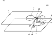
- FIG. 9 is a perspective view of the antenna device 103 according to the third embodiment.
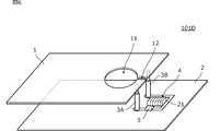
- FIG. 10 is a perspective view of an antenna device 104 according to the fourth embodiment.
- FIG. 11A is a perspective view of the antenna device 105 according to the fifth embodiment
- FIG. 11B is a front view of the antenna device 105.
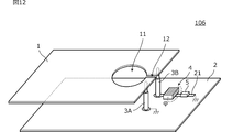
- FIG. 12 is a perspective view of an antenna device 106 according to the sixth embodiment.
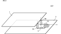
- FIG. 13 is a perspective view of an antenna device 107 according to the seventh embodiment.
- FIG. 14 is a partial perspective view of an antenna device 108A according to the eighth embodiment.
- FIG. 15 is a partial perspective view of another antenna device 108B according to the eighth embodiment.
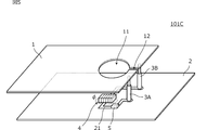
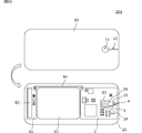
- FIG. 16 is a diagram illustrating the internal structure of the wireless communication device 201 according to the ninth embodiment, and is a plan view in a state where the lower housing 10 and the upper housing 20 are separated and the interior is exposed. It is.
- FIG. 1 is a perspective view of an antenna device 101A provided in a portable electronic device or the like according to the first embodiment.
- the antenna device 101 includes a conductive member 1 and a wiring board 2.
- the wiring board 2 is formed with a conductive coupling line 21 having conductivity.
- the conductive member 1 and the coupling line 21 are electrically connected via connection conductors 3A and 3B, which are spring pins, for example.
- the power supply coil 4 that is magnetically coupled to the coupling line 21 is mounted on the wiring board 2. Further, the chip capacitor 5 connected in series to the coupling line 21 is connected to the wiring board 2. In the present embodiment, a chip capacitor is used as a capacitor connected to the coupling line 21, but a lead-type capacitor or the like can also be used.
- the conductive member 1 is formed with a notch portion including a conductor opening 11 and a slit 12.
- the connection conductors 3A and 3B are connected to positions that sandwich (span) a notch (in particular, the slit 12 in the example shown in FIG. 1).
- FIG. 2 is a partial plan view showing a conductor pattern at the mounting position of the feeding coil 4 on the wiring board 2.
- a part of the coupled line 21 is formed as a terminal 22.
- Terminals 23 and 24 are formed on both sides of the terminal 22 portion of the coupled line 21 (both sides sandwiching the coupled line 21).
- the feeding coil 4 has three terminals on the mounting surface, and these three terminals are connected to the terminals 22, 23, and 24 of the wiring board 2.
- FIG. 3 is an exploded perspective view showing the configuration of the feeding coil 4.
- the feeding coil 4 is a laminated body of magnetic layers SH2a, SH2b, SH2c and nonmagnetic layers SH1a, SH1b.
- a plurality of linear conductors are formed on the magnetic layer SH2c and the non-magnetic layer SH1a, and via conductors connecting the linear conductors are formed on the magnetic layers SH2a, SH2b, and SH2c.
- These linear conductors and via conductors are coil conductors of the feeding coil 4.
- Input / output terminals 43 and 44 and a coupled line connection terminal 42 are formed on the lower surface of the nonmagnetic material layer SH1a.
- the ends of the outer linear conductors of the plurality of linear conductors formed on the magnetic layer SH2c are connected to the input / output terminals 43, 44. Via conductors are formed.
- the feeding coil 4 is configured as a chip component, and the terminals 42, 43, 44 on the lower surface are connected to the terminals 22, 23, 24 of the wiring board 2 shown in FIG.
- the coupling line connection terminal 42 of the feeding coil 4 is connected to the terminal 22 of the wiring board 2 but is not electrically connected to the coil conductor.
- the coil conductor of the feeding coil 4 and the coupling line 21 are magnetically coupled.
- the magnetic flux ⁇ represents this magnetic coupling.
- the winding axis of the feeding coil 4 is parallel to the surface of the wiring board 2 and is substantially orthogonal to the portion of the coupling line 21 to which the feeding coil 4 is close.
- the line width of the coupled line 21 is narrower than the coil winding width TW of the feeding coil 4.
- a current path is formed by the conductive member 1, the coupling line 21, and the connection conductors 3A and 3B.
- a current flows through the current path. That is, a current as indicated by a solid arrow in the drawing flows (distributes) through the conductive member 1 via the connection conductors 3A and 3B. In particular, the current concentrates along the edge of the conductor opening 11. As a result, a magnetic field as indicated by broken arrows and thick arrows in the figure is generated. This magnetic field couples to the communication partner antenna.
- the current induced in the conductive member 1 is taken out from the connection position of the connection conductors 3A and 3B.
- FIG. 4 is a perspective view of another antenna device 101B according to the first embodiment. What is different from the antenna device 101A shown in FIG. Also in this antenna device 101B, the winding axis of the feeding coil 4 is parallel to the surface of the wiring board 2 and is substantially orthogonal to the portion of the coupling line 21 to which the feeding coil 4 is close. For this reason, similarly to the antenna device 101A, the feeding coil 4 and the coupling line 21 are magnetically coupled to each other.
- FIG. 5 is a perspective view of still another antenna device 101C according to the first embodiment. What differs from the antenna devices 101 ⁇ / b> A and 101 ⁇ / b> B shown in the first embodiment is the arrangement position of the coupling line 21, the feeding coil 4 and the chip capacitor 5. The feeding coil 4 overlaps the conductive member 1 in plan view.
- the winding axis of the feeding coil 4 is parallel to the surface of the wiring board 2 and is substantially orthogonal to the portion of the coupling line 21 to which the feeding coil 4 is close. For this reason, similarly to the antenna devices 101A and 101B, the feeding coil 4 and the coupling line 21 are magnetically coupled to each other.
- FIG. 6 is a perspective view of still another antenna device 101D according to the first embodiment. What is different from the antenna device 101A shown in FIG. In this antenna device 101D, the feeding coil 4 and the coupling line 21 do not overlap in plan view.
- the feeding coil 4 has a winding axis substantially orthogonal to the coupling line 21. For this reason, as in the case of the antenna device 101A and the like, the feeding coil 4 and the coupling line 21 are magnetically coupled to each other.
- the feeding coil 4 may be disposed at a position where it is magnetically coupled to the coupling line 21. Therefore, the feeding coil 4 can be mounted on the wiring board 2 without being restricted by the positional relationship between the conductive member 1 and the notch (conductor opening 11, slit 12). In addition, the degree of coupling with the coupled line 21 can be optimized by determining the arrangement position of the feeding coil 4. Moreover, since the feeding coil 4 can be coupled to the coupling line 21 in a close state, the feeding coil 4 can be coupled more strongly than the coupling by the conductive member 1 and the notches (11, 12).
- the coupling line 21 is a conductor pattern and is thin, the magnetic flux generated from the feeding coil 4 is easily interlinked and can be strongly coupled. Since the feeding coil 4 and the coupling line 21 can be strongly coupled, the feeding coil 4 is smaller and has a lower inductance than the case where the feeding coil 4 is coupled to the conductive member 1 and the notches (11, 12). A thing with a weak radiation
- a configuration in which the secondary coil of the transformer is electrically directly connected in series to the coupling line 21 and a power feeding circuit is connected to the primary coil of the transformer is also conceivable. Due to the magnetic substance, the inductance ratio of the coupling line 21 is higher than the inductance of the conductive member 1. When the inductance ratio of the coupled line increases, the performance of the conductive member 1 as a radiating element deteriorates. On the other hand, according to this embodiment, since the inductance of the coupling line 21 can be reduced, the inductance contributing to the coupling with the communication partner antenna can be increased.
- the degree of coupling between the power feeding circuit and the antenna device is determined by the structure of the transformer, it is difficult to adjust the degree of coupling to obtain optimum performance.
- the degree of coupling for obtaining optimum performance can be easily determined by the position of the feeding coil with respect to the coupled line. Further, since bonding such as soldering to the coupled line is unnecessary, high reliability can be ensured.
- the mounting position of the power supply coil is limited to the vicinity of the springing pin, and the degree of freedom in the winding direction of the power supply coil for strong magnetic field coupling with the spring pin is low. .
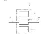
- FIG. 7 is a perspective view of an antenna device 102A according to the second embodiment.
- the antenna device 102 ⁇ / b> A includes a conductive member 1 and a wiring board 2.
- the wiring board 2 is formed with a conductive coupling line 21 having conductivity.
- the conductive member 1 and the coupling line 21 are electrically connected via connection conductors 3A and 3B.
- two feeding coils 4 ⁇ / b> A and 4 ⁇ / b> B that are magnetically coupled to the coupling line 21 are mounted. Further, the chip capacitor 5 connected in series to the coupling line 21 is connected to the wiring board 2.
- the configuration of the feeding coils 4A and 4B is as shown in FIG.
- the two power supply coils 4A and 4B are connected in series or in parallel and connected to the power supply circuit.
- three or more feeding coils may be provided. However, it is important to determine the polarity so that a plurality of feeding coils do not constitute a closed loop of magnetic flux. As described above, by providing a plurality of power supply coils, the degree of coupling between the antenna device and the power supply circuit can be easily increased. In the case of series connection, the size of each of the feeding coils 4A and 4B can be reduced, so that the space at the feeding coil arrangement position can be effectively utilized. In the case of parallel connection, the conductor loss can be reduced, so that the antenna characteristics can be improved.
- FIG. 8 is a perspective view of another antenna device 102B according to the second embodiment. Unlike the example shown in FIG. 1, two chip capacitors 5 ⁇ / b> A and 5 ⁇ / b> B are connected in series to the coupled line 21.
- this antenna device 102B When this antenna device 102B is applied to the HF band, for example, several thousand pF having a low withstand voltage is generally required, but a relatively high voltage of, for example, about 20 VAC is applied due to coupling with the other antenna during communication.
- a relatively high voltage of, for example, about 20 VAC is applied due to coupling with the other antenna during communication.
- a plurality of chip capacitors may be connected in parallel. As a result, the degree of freedom in setting the combined capacitance is increased, and fine setting of the resonance frequency of the antenna device is possible.
- FIG. 9 is a perspective view of the antenna device 103 according to the third embodiment.
- the antenna device 103 includes a conductive member 1 and a wiring board 2.
- the wiring board 2 is formed with a conductive coupling line 21 having conductivity.
- the conductive member 1 and the coupling line 21 are electrically connected via connection conductors 3A and 3B.
- a power supply coil 4 that is magnetically coupled to the coupling line 21 is mounted on the wiring board 2.
- the chip capacitor 5 connected in series to the coupling line 21 is connected to the wiring board 2.
- a ground pattern 26 is formed on the wiring board 2, and chip capacitors 6 A and 6 B are provided between the ground pattern 26 and the coupling line 21.
- the ground pattern 26 is formed in the vicinity of the connection position between the connection conductors 3A and 3B and the coupling line 21.
- the chip capacitors 6A and 6B are capacitances that can be regarded as equivalently open at the frequency (for example, 13.56 MHz) of a communication signal communicated by the antenna device 103, and equivalently regarded as short-circuited at a frequency (for example, UHF band) of other systems. It is. Therefore, in other systems, the base portions of the connection conductors 3A and 3B are grounded to the ground via the chip capacitors 6A and 6B.
- the conductive member 1 is grounded at a high frequency, the potential of the conductive member 1 is stabilized, and the electrostatic shielding effect is enhanced. Therefore, the influence on other systems can be minimized.
- the antenna device 103 is incorporated in a communication terminal device or the like together with a UHF band antenna for data communication or a telephone call, it is difficult to adversely affect the UHF band communication.
- FIG. 10 is a perspective view of an antenna device 104 according to the fourth embodiment.
- the antenna device 104 includes a conductive member 1 and a wiring board 2.
- the wiring board 2 is formed with a conductive coupling line 21 having conductivity.
- the conductive member 1 and the coupling line 21 are electrically connected via connection conductors 3A and 3B.
- a power supply coil 4 that is magnetically coupled to the coupling line 21 is mounted on the wiring board 2.
- the chip capacitor 5 connected in series to the coupling line 21 is connected to the wiring board 2.
- matching circuit components constituting the RFIC 7 and the matching circuit 8 are connected to the wiring board 2.
- the RFIC 7 and the matching circuit constituting the power feeding circuit may be provided on the wiring board 2 on which the coupling line 21 is formed.
- an antenna device integrated with a power feeding circuit can be configured.
- FIG. 11A is a perspective view of the antenna device 105 according to the fifth embodiment
- FIG. 11B is a front view of the antenna device 105.
- This antenna device 105 is incorporated in a portable antenna device or the like.
- the antenna device 105 includes a conductive member 1 and a wiring board 2.
- the wiring board 2 is formed with a conductive coupling line 21 having conductivity.
- the conductive member 1 and the coupling line 21 are electrically connected via connection conductors 3A and 3B.
- the power supply coil 4 that is magnetically coupled to the coupling line 21 is mounted on the wiring board 2. Further, the chip capacitor 5 connected in series to the coupling line 21 is connected to the wiring board 2.
- a magnetic sheet 9 such as a ferrite sheet is affixed in a position covering the vicinity of the notch (the conductor opening 11 and the slit 12), that is, the portion having a high current density (magnetic field strength).
- the magnetic sheet 9 If the magnetic sheet 9 is not present, an eddy current is induced in the ground electrode formed on the wiring board 2 by a magnetic field generated by a current flowing along the cutout portion of the conductive member 1, and thereby the conductive member 1. As a radiation element.
- the magnetic field due to the current flowing along the notch portion of the conductive member 1 is shielded by the magnetic sheet 9, so that the problem due to the eddy current can be avoided. .
- the magnetic sheet 9 is not limited to a shape that covers the notch, but may have a shape that covers only the periphery of the notch, that is, a shape that does not cover the conductor opening 11 and the slit 12. Even if the magnetic sheet 9 has a shape that covers only the periphery of the notch, it is possible to obtain a certain degree of effect of suppressing the eddy current.
- FIG. 12 is a perspective view of an antenna device 106 according to the sixth embodiment. Unlike the antenna devices 101A, 101B, etc. shown in the first embodiment, the antenna device 106 uses a ground conductor as a part of the current path.
- a part or end of the coupled line 21 is connected to the ground conductor of the wiring board 2
- the connection conductor 3 ⁇ / b> A is also connected to the ground conductor of the wiring board 2. Therefore, a current path is constituted by the conductive member 1, the connection conductors 3A and 3B, the coupling line 21 and the ground conductor.
- the coupling line 21 formed on the wiring board 2 it is not necessary to route the coupling line 21 formed on the wiring board 2, and the substantial occupied area of the coupling line 21 with respect to the wiring board 2 can be reduced.
- the ground conductor is formed over the entire surface of the wiring board 2
- the conductive member 1 and the coupling line 21 are connected to the ground conductor at an arbitrary position of the conductive member 1 via the connection conductors 3A and 3B. Is possible. Therefore, the degree of freedom of arrangement of the connection conductors 3A and 3B, the coupling line 21, the feeding coil 4, and the chip capacitor 5 is increased.
- a current path having an arbitrary shape can be formed by the conductive member 1, the connecting conductors 3A and 3B, the coupling line 21, and the ground conductor, and the degree of freedom in design related to the radiation characteristics of the antenna device is increased.
- FIG. 13 is a perspective view of an antenna device 107 according to the seventh embodiment. Unlike the antenna devices 101A and 101B shown in the first embodiment, the antenna device 107 does not have the conductor openings 11 and the slits 12 formed in the conductive member 1.
- the conductor opening 11 and the slit 12 are not essential.
- the antenna device 107 of the present embodiment when the antenna device 107 transmits, magnetic flux is radiated from the loop formed by the current path formed by the coupling line 21, the connection conductors 3A and 3B, and the conductive member 1. Further, when the antenna device 107 is receiving, the magnetic flux generated from the communication partner antenna passes through the loop formed by the coupling line 21, the connection conductors 3 ⁇ / b> A and 3 ⁇ / b> B, and the conductive member 1. The antenna on the other end of communication is coupled
- FIG. 14 is a partial perspective view of an antenna device 108A according to the eighth embodiment.
- the antenna device 108A includes two conductive members 1A and 1B.
- the conductive members 1 ⁇ / b> A and 1 ⁇ / b> B are part of a housing that houses the wiring board 2.
- the conductive member 1A constitutes a main part of the casing
- the conductive member 1B constitutes a main surface and part of both side faces and an end face of the casing.
- Coupling lines 21A and 21B are formed on the wiring board 2.
- the feeding coil 4 is mounted (placed) at a position where it is coupled to the coupling line 21A, and the chip capacitor 5 is connected in series to the coupling line 21B.
- the shapes of the conductive members 1A and 1B are not limited to those illustrated in FIG. 14, and may be shapes with rounded corners.
- the coupling lines 21A and 21B are electrically connected to the conductive member 1A via the connection conductors 3A and 3B, and are electrically connected to the conductive member 1B via the connection conductors 3C and 3D. Therefore, a current path is constituted by the coupled lines 21A and 21B and the conductive members 1A and 1B.
- FIG. 15 is a partial perspective view of another antenna device 108B according to the eighth embodiment.
- the antenna device 108B includes two conductive members 1A and 1C.
- the conductive members 1 ⁇ / b> A and 1 ⁇ / b> C are part of a housing that houses the wiring board 2.
- the conductive member 1A constitutes a main part of the casing, and the conductive member 1B constitutes part of both side surfaces and end faces of the casing.
- Coupling lines 21A and 21B are formed on the wiring board 2.
- the feeding coil 4 is mounted (placed) at a position where it is coupled to the coupling line 21A, and the chip capacitor 5 is connected in series to the coupling line 21B.
- the coupling lines 21A and 21B are electrically connected to the conductive member 1A through the connection conductors 3A and 3B.
- the coupled lines 21A and 21B are connected to the conductive member 1C. Therefore, a current path is constituted by the coupled lines 21A and 21B and the conductive members 1A and 1C.
- the conductive members 1A, 1B, and 1C are, for example, a metal casing of a wireless communication device in which the antenna device 108B is mounted.
- the conductive members 1B and 1C may use a radiating element that functions as a standing wave antenna such as a UHF band of a wireless communication device.
- a standing wave type antenna is an antenna that resonates with a radiating element and radiates an electromagnetic wave by distributing a standing wave of voltage and current.
- An inverted F type antenna, a monopole antenna, a single wavelength loop antenna, Patch antennas such as L-shaped antennas, plate-like inverted F antennas (PIFA), slot antennas, notch antennas, and the like are included.
- FIG. 16 is a diagram illustrating a structure inside the housing of the wireless communication device 201 according to the sixth embodiment which is an example of the antenna device of the present invention.
- the lower housing 10 and the upper housing 20 are separated from each other. It is a top view in the state where the inside was exposed.
- wiring boards 2, 81, a battery pack 83, and the like are housed in the upper housing 20, wiring boards 2, 81, a battery pack 83, and the like are housed.
- a coupling line 21 is formed on the wiring board 2, and connection conductors 3 ⁇ / b> A and 3 ⁇ / b> B that are spring pins, a feeding coil 4, a chip capacitor 5, an RFIC, and the like are mounted (connected).
- a camera module 85 and the like are also mounted on the wiring board 2.
- the UHF band antenna 82 and the like are mounted on the wiring board 81.
- the wiring board 2 and the wiring board 81 are connected via a coaxial cable 84.
- a conductor opening 11 and a slit 12 are formed in the lower housing 10.
- the conductor opening 11 is formed at a position facing the camera module 85.
- the connection conductors 3 ⁇ / b> A and 3 ⁇ / b> B come into contact with the position of the lower housing 10 across the slit 12. Note that other devices such as buttons and speakers may be arranged in the conductor openings 11.
- the lower housing 10 acts as a radiating element.
- the coupling line 21 is on a layer different from the mounting surface of the feeding coil 4. It may be formed.
- the feeding coil 4 may be disposed on the back surface of the wiring board 2.
- the wiring board 2 may be a multilayer board, and the coupling line 21 may be formed in the inner layer.
- the example in which the coil conductor of the feeding coil 4 is magnetically coupled to one of the coupling lines 21 has been shown.
- a planar coil pattern having a plurality of turns is formed, and the coil conductor of the feeding coil 4 is formed. May be configured to be magnetically coupled to a plurality of coupled lines.
- the wiring board 2 is a multilayer board, a plurality of turns of the coupling line 21 is formed by using a plurality of layers of the wiring board, and the coil conductor of the feeding coil 4 is magnetically coupled to the plurality of coupling lines. Also good.
- the inductance and resistance of the coupled line may be reduced by narrowing the line width of the coupled line 21 where the feeding coil 4 is coupled and increasing the line width of the uncoupled part. Further, the inductance and resistance of the coupled line may be reduced by increasing the number of lines and the number of layers in the part that is not coupled.
- the coupled line has a U-shape. Further, it may be curved.
- the conductor opening 11 formed in the conductive member 1 is an opening facing the camera module.
- the hole for the operation button or the hole for the earphone jack on the side surface of the housing is made conductive. It may be used as a conductor opening of the member 1.
- connection conductors 3A and 3B may be connected to two portions of the conductive member having no notch. In this case, the current concentrates along the edge of the conductive member 1 due to the edge effect. At the time of transmission, a distributed current flows through the conductive member 1, whereby a magnetic field is radiated from the conductive member 1, and at the time of reception, a current induced in the conductive member 1 is extracted from the connection position of the connection conductors 3A and 3B.
- Coiled conductor 42 ... Coupling line connection terminals 43, 44 ... Input / output terminal 81 ... Wiring board 82 ... UHF band antenna 83 ... Battery pack 84 ... Coaxial cable 85 ... Camera module 101 ... Antenna devices 101A to 101D ... Antenna devices 102A and 102B ... Antenna devices 103 to 108A and 108B ... Antenna device 201 ... Wireless communication device
Abstract
Description
図1は第1の実施形態に係る携帯電子機器等に備えられるアンテナ装置101Aの斜視図である。このアンテナ装置101は、導電性部材1と配線基板2とを備える。配線基板2には導電性を有する結合線路21が形成されている。導電性部材1と結合線路21とは、例えばスプリングピンである接続導体3A,3Bを介して電気的に接続されている。 << First Embodiment >>
FIG. 1 is a perspective view of an
図7は第2の実施形態に係るアンテナ装置102Aの斜視図である。アンテナ装置102Aは、導電性部材1と配線基板2とを備える。配線基板2には導電性を有する結合線路21が形成されている。導電性部材1と結合線路21とは接続導体3A,3Bを介して電気的に接続されている。配線基板2には、結合線路21に対して磁界結合する2つの給電コイル4A,4Bが実装されている。また、配線基板2には、結合線路21に対して直列接続されるチップキャパシタ5が接続されている。 << Second Embodiment >>
FIG. 7 is a perspective view of an
図9は第3の実施形態に係るアンテナ装置103の斜視図である。アンテナ装置103は、導電性部材1と配線基板2とを備える。配線基板2には導電性を有する結合線路21が形成されている。導電性部材1と結合線路21とは接続導体3A,3Bを介して電気的に接続されている。配線基板2には、結合線路21と磁界結合する給電コイル4が実装されている。また、配線基板2には、結合線路21に対して直列接続されるチップキャパシタ5が接続されている。 << Third Embodiment >>
FIG. 9 is a perspective view of the
図10は第4の実施形態に係るアンテナ装置104の斜視図である。アンテナ装置104は、導電性部材1と配線基板2とを備える。配線基板2には導電性を有する結合線路21が形成されている。導電性部材1と結合線路21とは接続導体3A,3Bを介して電気的に接続されている。配線基板2には、結合線路21と磁界結合する給電コイル4が実装されている。また、配線基板2には、結合線路21に対して直列接続されるチップキャパシタ5が接続されている。更に、配線基板2にはRFIC7および整合回路8を構成する整合回路部品が接続されている。 << Fourth Embodiment >>
FIG. 10 is a perspective view of an
図11(A)は第5の実施形態に係るアンテナ装置105の斜視図であり、図11(B)はアンテナ装置105の正面図である。このアンテナ装置105は、携帯アンテナ装置等に組み込まれる。アンテナ装置105は、導電性部材1と配線基板2とを備える。配線基板2には導電性を有する結合線路21が形成されている。導電性部材1と結合線路21とは接続導体3A,3Bを介して電気的に接続されている。 << Fifth Embodiment >>
FIG. 11A is a perspective view of the
図12は第6の実施形態に係るアンテナ装置106の斜視図である。アンテナ装置106は、第1の実施形態で示したアンテナ装置101A,101B等と異なり、グランド導体を電流経路の一部に利用している。図12において、結合線路21の一部または端部が配線基板2のグランド導体に接続され、接続導体3Aも配線基板2のグランド導体に接続される。したがって、導電性部材1、接続導体3A,3B、結合線路21およびグランド導体によって電流経路が構成される。 << Sixth Embodiment >>
FIG. 12 is a perspective view of an
図13は第7の実施形態に係るアンテナ装置107の斜視図である。アンテナ装置107は、第1の実施形態で示したアンテナ装置101A,101Bと異なり、導電性部材1に導体開口11およびスリット12を形成していない。 << Seventh Embodiment >>
FIG. 13 is a perspective view of an
図14は第8の実施形態に係るアンテナ装置108Aの部分斜視図である。アンテナ装置108Aは、2つの導電性部材1A,1Bを備える。導電性部材1A,1Bは配線基板2を内部に収める筐体の一部である。導電性部材1Aは筺体の主要部を構成し、導電性部材1Bは筺体の主面および両側面の一部、ならびに端面を構成する。配線基板2には結合線路21A,21Bが形成されている。配線基板2には、結合線路21Aと結合する位置に給電コイル4が実装(載置)され、結合線路21Bにチップキャパシタ5が直列に接続される。なお、導電性部材1Aおよび1Bの形状は図14に図示されているものには限られず、角が丸みを帯びている形状であってもよい。 << Eighth Embodiment >>
FIG. 14 is a partial perspective view of an
図16は、本発明のアンテナ装置の一例である第6の実施形態に係る無線通信装置201の筐体内部の構造を示す図であり、下部筐体10と上部筐体20とを分離して内部を露出させた状態での平面図である。上部筐体20の内部には配線基板2,81、バッテリーパック83等が収められている。配線基板2には結合線路21が形成されていて、スプリングピンである接続導体3A,3B、給電コイル4、チップキャパシタ5、RFIC等が実装(接続)されている。この配線基板2にはカメラモジュール85等も搭載されている。また、配線基板81にはUHF帯アンテナ82等が搭載されている。配線基板2と配線基板81とは同軸ケーブル84を介して接続されている。 << Ninth embodiment >>
FIG. 16 is a diagram illustrating a structure inside the housing of the
以上に示した各実施形態では、結合線路21を配線基板2の表面(給電コイル4の実装面)に形成した例を示したが、結合線路21は給電コイル4の実装面とは異なる層に形成してもよい。例えば、図1において、給電コイル4を配線基板2の裏面に配置してもよい。また、配線基板2を多層基板とし、内層に結合線路21を形成してもよい。 << Other embodiments >>
In each embodiment shown above, although the example which formed the
SH2a,SH2b,SH2c…磁性体層
TW…コイル巻回幅
1…導電性部材
2…配線基板
2,81…配線基板
3A,3B…接続導体
4,4A,4B…給電コイル
5,5A,5B…チップキャパシタ
6A,6B…チップキャパシタ
7…RFIC
8…整合回路
9…磁性体シート
10…下部筐体
11…導体開口
12…スリット
(11,12)…切り欠き部
20…上部筐体
21,21A,21B…結合線路
22,23,24…端子
26…グランドパターン
40…コイル状導体
42…結合線路接続端子
43,44…入出力端子
81…配線基板
82…UHF帯アンテナ
83…バッテリーパック
84…同軸ケーブル
85…カメラモジュール
101…アンテナ装置
101A~101D…アンテナ装置
102A,102B…アンテナ装置
103~108A,108B…アンテナ装置
201…無線通信装置 SH1a, SH1b ... nonmagnetic layers SH2a, SH2b, SH2c ... magnetic layer TW ...
DESCRIPTION OF
Claims (13)
- 導電性部材と、
導電性を有する結合線路を含む配線基板と、
前記導電性部材と前記結合線路とを電気的に接続する接続導体と、
前記配線基板に設けられ、前記結合線路と磁界結合する給電コイルと、
を備え、少なくとも前記導電性部材、前記結合線路および前記接続導体によって電流経路が形成されたことを特徴とするアンテナ装置。 A conductive member;
A wiring board including a coupling line having conductivity; and
A connection conductor for electrically connecting the conductive member and the coupling line;
A power feeding coil provided on the wiring board and magnetically coupled to the coupling line;
An antenna device characterized in that a current path is formed by at least the conductive member, the coupling line, and the connection conductor. - 前記結合線路の一端はグランド電極に接続され、少なくとも前記導電性部材と前記接続導体と前記結合線路と前記グランド電極とによって前記電流経路が形成される、請求項1に記載のアンテナ装置。 The antenna device according to claim 1, wherein one end of the coupling line is connected to a ground electrode, and the current path is formed by at least the conductive member, the connection conductor, the coupling line, and the ground electrode.
- 前記導電性部材は切り欠き部を備え、前記接続導体は前記切り欠き部を挟む位置に複数設けられている、請求項1または2に記載のアンテナ装置。 The antenna device according to claim 1 or 2, wherein the conductive member includes a notch, and a plurality of the connection conductors are provided at positions sandwiching the notch.
- 前記導電性部材の前記切り欠き部近傍を覆う磁性体シートをさらに備えた、請求項3に記載のアンテナ装置。 The antenna device according to claim 3, further comprising a magnetic sheet that covers the vicinity of the notch of the conductive member.
- 前記配線基板に、前記結合線路に接続されるキャパシタが搭載された、請求項1~4のいずれかに記載のアンテナ装置。 The antenna device according to any one of claims 1 to 4, wherein a capacitor connected to the coupling line is mounted on the wiring board.
- 前記給電コイルの巻回軸は前記配線基板の面に対してほぼ平行である、請求項1~5のいずれかに記載のアンテナ装置。 The antenna device according to any one of claims 1 to 5, wherein a winding axis of the feeding coil is substantially parallel to a surface of the wiring board.
- 前記結合線路の少なくとも一部は、前記給電コイルの近傍において前記給電コイルの巻回軸に対してほぼ直交している、請求項1~6のいずれかに記載のアンテナ装置。 7. The antenna device according to claim 1, wherein at least a part of the coupling line is substantially orthogonal to a winding axis of the feeding coil in the vicinity of the feeding coil.
- 前記配線基板に、前記接続導体に繋がり、高周波信号をグランドへバイパスするキャパシタを設けた、請求項1~7のいずれかに記載のアンテナ装置。 8. The antenna device according to claim 1, wherein a capacitor connected to the connection conductor and bypassing a high-frequency signal to the ground is provided on the wiring board.
- 前記給電コイルは、前記給電コイルの入出力端子とは絶縁された結合線路接続端子を備え、前記給電コイルの結合線路接続端子は前記結合線路にはんだ付けされている、請求項1~8のいずれかに記載のアンテナ装置。 9. The feed coil according to claim 1, wherein the feed coil includes a coupled line connection terminal insulated from an input / output terminal of the feed coil, and the coupled line connection terminal of the feed coil is soldered to the coupled line. An antenna device according to claim 1.
- 前記配線基板は多層基板であり、前記結合線路は前記給電コイルの実装面とは異なる層に形成されている、請求項1~9のいずれかに記載のアンテナ装置。 The antenna device according to any one of claims 1 to 9, wherein the wiring board is a multilayer board, and the coupling line is formed in a layer different from a mounting surface of the feeding coil.
- 前記給電コイルに接続される給電回路を前記配線基板に備えた、請求項1~10のいずれかに記載のアンテナ装置。 The antenna device according to any one of claims 1 to 10, wherein a power supply circuit connected to the power supply coil is provided on the wiring board.
- アンテナ装置を備える電子機器であり、
前記アンテナ装置は、導電性部材と、導電性を有する結合線路を含む配線基板と、
前記導電性部材と前記結合線路とを電気的に接続する接続導体と、前記配線基板に設けられ、前記結合線路と磁界結合する給電コイルと、を備え、少なくとも前記導電性部材、前記結合線路および前記接続導体によって電流経路が形成されたことを特徴とする電子機器。 An electronic device including an antenna device;
The antenna device includes a conductive member, a wiring board including a conductive coupling line,
A connection conductor that electrically connects the conductive member and the coupling line; and a feeding coil that is provided on the wiring board and magnetically couples to the coupling line, and includes at least the conductive member, the coupling line, and An electronic apparatus, wherein a current path is formed by the connection conductor. - 前記導電性部材は前記配線基板を収める筐体の一部である、請求項12に記載の電子機器。 The electronic device according to claim 12, wherein the conductive member is a part of a housing that houses the wiring board.
Priority Applications (4)
| Application Number | Priority Date | Filing Date | Title |
|---|---|---|---|
| CN201580023080.5A CN106463832B (en) | 2014-04-30 | 2015-04-21 | Antenna assembly and electronic equipment |
| EP15785998.4A EP3125367B1 (en) | 2014-04-30 | 2015-04-21 | Antenna device and electronic device |
| JP2016516322A JP6256600B2 (en) | 2014-04-30 | 2015-04-21 | ANTENNA DEVICE AND ELECTRONIC DEVICE |
| US15/297,195 US10062956B2 (en) | 2014-04-30 | 2016-10-19 | Antenna device and electronic apparatus |
Applications Claiming Priority (2)
| Application Number | Priority Date | Filing Date | Title |
|---|---|---|---|
| JP2014093324 | 2014-04-30 | ||
| JP2014-093324 | 2014-04-30 |
Related Child Applications (1)
| Application Number | Title | Priority Date | Filing Date |
|---|---|---|---|
| US15/297,195 Continuation US10062956B2 (en) | 2014-04-30 | 2016-10-19 | Antenna device and electronic apparatus |
Publications (1)
| Publication Number | Publication Date |
|---|---|
| WO2015166834A1 true WO2015166834A1 (en) | 2015-11-05 |
Family
ID=54358565
Family Applications (1)
| Application Number | Title | Priority Date | Filing Date |
|---|---|---|---|
| PCT/JP2015/062037 WO2015166834A1 (en) | 2014-04-30 | 2015-04-21 | Antenna device and electronic device |
Country Status (5)
| Country | Link |
|---|---|
| US (1) | US10062956B2 (en) |
| EP (1) | EP3125367B1 (en) |
| JP (1) | JP6256600B2 (en) |
| CN (1) | CN106463832B (en) |
| WO (1) | WO2015166834A1 (en) |
Cited By (11)
| Publication number | Priority date | Publication date | Assignee | Title |
|---|---|---|---|---|
| CN106207442A (en) * | 2016-06-29 | 2016-12-07 | 青岛海信移动通信技术股份有限公司 | The NFC antenna of a kind of mobile terminal and mobile terminal |
| CN106207441A (en) * | 2016-06-29 | 2016-12-07 | 青岛海信移动通信技术股份有限公司 | The NFC antenna of a kind of mobile terminal and mobile terminal |
| CN106299610A (en) * | 2016-10-21 | 2017-01-04 | 珠海市魅族科技有限公司 | The antenna assembly of a kind of electronic equipment and electronic equipment |
| CN106450697A (en) * | 2016-10-21 | 2017-02-22 | 珠海市魅族科技有限公司 | Antenna apparatus of electronic equipment and the electronic equipment |
| WO2017122764A1 (en) * | 2016-01-14 | 2017-07-20 | 株式会社村田製作所 | Antenna device and electronic apparatus |
| CN107342268A (en) * | 2016-04-29 | 2017-11-10 | 台湾积体电路制造股份有限公司 | Semiconductor device packages |
| WO2018030363A1 (en) * | 2016-08-10 | 2018-02-15 | 株式会社村田製作所 | Antenna device and electronic instrument |
| WO2018056422A1 (en) * | 2016-09-26 | 2018-03-29 | 株式会社村田製作所 | Antenna device and electronic equipment |
| WO2018056101A1 (en) * | 2016-09-26 | 2018-03-29 | 株式会社村田製作所 | Antenna device and electronic instrument |
| WO2018181042A1 (en) * | 2017-03-27 | 2018-10-04 | 株式会社村田製作所 | Antenna device and electronic apparatus |
| WO2020250477A1 (en) * | 2019-06-12 | 2020-12-17 | 株式会社村田製作所 | Rfid tag and article with rfid tag |
Families Citing this family (8)
| Publication number | Priority date | Publication date | Assignee | Title |
|---|---|---|---|---|
| US9716307B2 (en) * | 2012-11-08 | 2017-07-25 | Htc Corporation | Mobile device and antenna structure |
| KR101619322B1 (en) * | 2015-01-05 | 2016-05-10 | 주식회사 아모텍 | Nfc antenna module using metal case |
| JP6518285B2 (en) | 2017-05-01 | 2019-05-22 | 原田工業株式会社 | Antenna device |
| JP2018201165A (en) * | 2017-05-29 | 2018-12-20 | 株式会社リコー | Antenna device and method for manufacturing the same |
| KR102121795B1 (en) * | 2018-05-04 | 2020-06-11 | 주식회사 아모텍 | Antenna module |
| CN111081463B (en) * | 2018-10-19 | 2021-01-26 | 立锜科技股份有限公司 | Transmission interface with noise reduction |
| JP6678722B1 (en) * | 2018-10-31 | 2020-04-08 | 京セラ株式会社 | Antenna, wireless communication module and wireless communication device |
| CN112803147B (en) * | 2019-11-14 | 2023-05-05 | 华为技术有限公司 | Antenna and mobile terminal |
Citations (5)
| Publication number | Priority date | Publication date | Assignee | Title |
|---|---|---|---|---|
| JPH08195618A (en) * | 1995-01-13 | 1996-07-30 | Citizen Watch Co Ltd | Antenna structure of portable electronic equipment |
| WO2013042604A1 (en) * | 2011-09-20 | 2013-03-28 | 株式会社村田製作所 | Electronic equipment |
| JP5246764B2 (en) * | 2008-10-16 | 2013-07-24 | 国立大学法人 東京大学 | Wireless communication device |
| WO2014003163A1 (en) * | 2012-06-28 | 2014-01-03 | 株式会社村田製作所 | Antenna device and communication terminal device |
| JP5403146B2 (en) * | 2010-03-03 | 2014-01-29 | 株式会社村田製作所 | Wireless communication device and wireless communication terminal |
Family Cites Families (8)
| Publication number | Priority date | Publication date | Assignee | Title |
|---|---|---|---|---|
| FI119010B (en) * | 2006-01-09 | 2008-06-13 | Pulse Finland Oy | RFID antenna |
| CN103022661B (en) | 2009-04-21 | 2014-12-03 | 株式会社村田制作所 | Antenna apparatus and resonant frequency setting method of same |
| WO2011090080A1 (en) * | 2010-01-19 | 2011-07-28 | 株式会社村田製作所 | Antenna device and communication terminal apparatus |
| WO2011090082A1 (en) * | 2010-01-19 | 2011-07-28 | 株式会社村田製作所 | Transformer having high degree of coupling, electronic circuit and electronic device |
| JP5758909B2 (en) * | 2010-10-12 | 2015-08-05 | 株式会社村田製作所 | Communication terminal device |
| JP5772868B2 (en) | 2012-05-21 | 2015-09-02 | 株式会社村田製作所 | ANTENNA DEVICE AND WIRELESS COMMUNICATION DEVICE |
| CN105975889B (en) * | 2012-06-28 | 2020-01-03 | 株式会社村田制作所 | Antenna device and communication terminal device |
| CN206163716U (en) * | 2014-03-28 | 2017-05-10 | 株式会社村田制作所 | Antenna device and communication equipment |
-
2015
- 2015-04-21 JP JP2016516322A patent/JP6256600B2/en active Active
- 2015-04-21 WO PCT/JP2015/062037 patent/WO2015166834A1/en active Application Filing
- 2015-04-21 CN CN201580023080.5A patent/CN106463832B/en active Active
- 2015-04-21 EP EP15785998.4A patent/EP3125367B1/en active Active
-
2016
- 2016-10-19 US US15/297,195 patent/US10062956B2/en active Active
Patent Citations (5)
| Publication number | Priority date | Publication date | Assignee | Title |
|---|---|---|---|---|
| JPH08195618A (en) * | 1995-01-13 | 1996-07-30 | Citizen Watch Co Ltd | Antenna structure of portable electronic equipment |
| JP5246764B2 (en) * | 2008-10-16 | 2013-07-24 | 国立大学法人 東京大学 | Wireless communication device |
| JP5403146B2 (en) * | 2010-03-03 | 2014-01-29 | 株式会社村田製作所 | Wireless communication device and wireless communication terminal |
| WO2013042604A1 (en) * | 2011-09-20 | 2013-03-28 | 株式会社村田製作所 | Electronic equipment |
| WO2014003163A1 (en) * | 2012-06-28 | 2014-01-03 | 株式会社村田製作所 | Antenna device and communication terminal device |
Cited By (25)
| Publication number | Priority date | Publication date | Assignee | Title |
|---|---|---|---|---|
| CN107534218B (en) * | 2016-01-14 | 2019-05-17 | 株式会社村田制作所 | Antenna assembly and electronic equipment |
| CN110120583A (en) * | 2016-01-14 | 2019-08-13 | 株式会社村田制作所 | Antenna assembly and electronic equipment |
| DE112017000032B4 (en) | 2016-01-14 | 2019-10-02 | Murata Manufacturing Co., Ltd. | ANTENNA DEVICE AND ELECTRONIC APPARATUS |
| US10276936B2 (en) | 2016-01-14 | 2019-04-30 | Murata Manufacturing Co., Ltd. | Antenna device and electronic apparatus |
| CN107534218A (en) * | 2016-01-14 | 2018-01-02 | 株式会社村田制作所 | Antenna assembly and electronic equipment |
| WO2017122764A1 (en) * | 2016-01-14 | 2017-07-20 | 株式会社村田製作所 | Antenna device and electronic apparatus |
| JP6237968B1 (en) * | 2016-01-14 | 2017-11-29 | 株式会社村田製作所 | ANTENNA DEVICE AND ELECTRONIC DEVICE |
| KR101822548B1 (en) | 2016-01-14 | 2018-01-26 | 가부시키가이샤 무라타 세이사쿠쇼 | Antenna devices and electronic devices |
| CN107342268A (en) * | 2016-04-29 | 2017-11-10 | 台湾积体电路制造股份有限公司 | Semiconductor device packages |
| CN106207441A (en) * | 2016-06-29 | 2016-12-07 | 青岛海信移动通信技术股份有限公司 | The NFC antenna of a kind of mobile terminal and mobile terminal |
| CN106207442A (en) * | 2016-06-29 | 2016-12-07 | 青岛海信移动通信技术股份有限公司 | The NFC antenna of a kind of mobile terminal and mobile terminal |
| WO2018030363A1 (en) * | 2016-08-10 | 2018-02-15 | 株式会社村田製作所 | Antenna device and electronic instrument |
| JP6369666B1 (en) * | 2016-09-26 | 2018-08-08 | 株式会社村田製作所 | ANTENNA DEVICE AND ELECTRONIC DEVICE |
| JP6376317B1 (en) * | 2016-09-26 | 2018-08-22 | 株式会社村田製作所 | ANTENNA DEVICE AND ELECTRONIC DEVICE |
| WO2018056101A1 (en) * | 2016-09-26 | 2018-03-29 | 株式会社村田製作所 | Antenna device and electronic instrument |
| WO2018056422A1 (en) * | 2016-09-26 | 2018-03-29 | 株式会社村田製作所 | Antenna device and electronic equipment |
| US10505267B2 (en) | 2016-09-26 | 2019-12-10 | Murata Manufacturing Co., Ltd. | Antenna device and electronic apparatus |
| US10530057B2 (en) | 2016-09-26 | 2020-01-07 | Murata Manufacturing, Co., Ltd. | Antenna device and electronic appliance |
| CN106299610A (en) * | 2016-10-21 | 2017-01-04 | 珠海市魅族科技有限公司 | The antenna assembly of a kind of electronic equipment and electronic equipment |
| CN106450697A (en) * | 2016-10-21 | 2017-02-22 | 珠海市魅族科技有限公司 | Antenna apparatus of electronic equipment and the electronic equipment |
| CN106299610B (en) * | 2016-10-21 | 2019-01-22 | 珠海市魅族科技有限公司 | The antenna assembly and electronic equipment of a kind of electronic equipment |
| WO2018181042A1 (en) * | 2017-03-27 | 2018-10-04 | 株式会社村田製作所 | Antenna device and electronic apparatus |
| JP6428990B1 (en) * | 2017-03-27 | 2018-11-28 | 株式会社村田製作所 | ANTENNA DEVICE AND ELECTRONIC DEVICE |
| US11132593B2 (en) | 2019-06-12 | 2021-09-28 | Murata Manufacturing Co., Ltd. | RFID tag and RFID tag-equipped article |
| WO2020250477A1 (en) * | 2019-06-12 | 2020-12-17 | 株式会社村田製作所 | Rfid tag and article with rfid tag |
Also Published As
| Publication number | Publication date |
|---|---|
| CN106463832A (en) | 2017-02-22 |
| JP6256600B2 (en) | 2018-01-10 |
| CN106463832B (en) | 2019-04-26 |
| EP3125367A4 (en) | 2017-11-08 |
| JPWO2015166834A1 (en) | 2017-04-20 |
| US20170040663A1 (en) | 2017-02-09 |
| EP3125367A1 (en) | 2017-02-01 |
| EP3125367B1 (en) | 2019-07-31 |
| US10062956B2 (en) | 2018-08-28 |
Similar Documents
| Publication | Publication Date | Title |
|---|---|---|
| JP6256600B2 (en) | ANTENNA DEVICE AND ELECTRONIC DEVICE | |
| US10033104B2 (en) | Antenna device and wireless communication device | |
| JP6260729B2 (en) | Feeding element | |
| JP5773021B2 (en) | Antenna device | |
| JP5360202B2 (en) | Antenna device | |
| JP5522227B2 (en) | Mobile communication terminal | |
| JP5924006B2 (en) | Antenna device | |
| JP6311833B2 (en) | Antenna device | |
| WO2012014939A1 (en) | Antenna device and communications terminal device | |
| JP2013055637A (en) | Antenna device and communication terminal device | |
| JP2013168894A (en) | Antenna device and communication terminal having the same | |
| WO2016186092A1 (en) | Antenna device and electronic apparatus | |
| WO2016186090A1 (en) | Antenna device and electronic apparatus |
Legal Events
| Date | Code | Title | Description |
|---|---|---|---|
| 121 | Ep: the epo has been informed by wipo that ep was designated in this application |
Ref document number: 15785998 Country of ref document: EP Kind code of ref document: A1 |
|
| REEP | Request for entry into the european phase |
Ref document number: 2015785998 Country of ref document: EP |
|
| WWE | Wipo information: entry into national phase |
Ref document number: 2015785998 Country of ref document: EP |
|
| ENP | Entry into the national phase |
Ref document number: 2016516322 Country of ref document: JP Kind code of ref document: A |
|
| NENP | Non-entry into the national phase |
Ref country code: DE |