EP2388839A2 - Wavelength conversion layer between a reflective layer and the light-emitting diode layers. - Google Patents
Wavelength conversion layer between a reflective layer and the light-emitting diode layers. Download PDFInfo
- Publication number
- EP2388839A2 EP2388839A2 EP11166278A EP11166278A EP2388839A2 EP 2388839 A2 EP2388839 A2 EP 2388839A2 EP 11166278 A EP11166278 A EP 11166278A EP 11166278 A EP11166278 A EP 11166278A EP 2388839 A2 EP2388839 A2 EP 2388839A2
- Authority
- EP
- European Patent Office
- Prior art keywords
- light
- layer
- emitting device
- luminescence
- emitting
- Prior art date
- Legal status (The legal status is an assumption and is not a legal conclusion. Google has not performed a legal analysis and makes no representation as to the accuracy of the status listed.)
- Granted
Links
Images





Classifications
-
- H—ELECTRICITY
- H10—SEMICONDUCTOR DEVICES; ELECTRIC SOLID-STATE DEVICES NOT OTHERWISE PROVIDED FOR
- H10H—INORGANIC LIGHT-EMITTING SEMICONDUCTOR DEVICES HAVING POTENTIAL BARRIERS
- H10H20/00—Individual inorganic light-emitting semiconductor devices having potential barriers, e.g. light-emitting diodes [LED]
- H10H20/80—Constructional details
- H10H20/85—Packages
- H10H20/851—Wavelength conversion means
-
- H—ELECTRICITY
- H10—SEMICONDUCTOR DEVICES; ELECTRIC SOLID-STATE DEVICES NOT OTHERWISE PROVIDED FOR
- H10H—INORGANIC LIGHT-EMITTING SEMICONDUCTOR DEVICES HAVING POTENTIAL BARRIERS
- H10H20/00—Individual inorganic light-emitting semiconductor devices having potential barriers, e.g. light-emitting diodes [LED]
- H10H20/80—Constructional details
- H10H20/84—Coatings, e.g. passivation layers or antireflective coatings
- H10H20/841—Reflective coatings, e.g. dielectric Bragg reflectors
-
- H—ELECTRICITY
- H10—SEMICONDUCTOR DEVICES; ELECTRIC SOLID-STATE DEVICES NOT OTHERWISE PROVIDED FOR
- H10H—INORGANIC LIGHT-EMITTING SEMICONDUCTOR DEVICES HAVING POTENTIAL BARRIERS
- H10H20/00—Individual inorganic light-emitting semiconductor devices having potential barriers, e.g. light-emitting diodes [LED]
- H10H20/80—Constructional details
- H10H20/81—Bodies
- H10H20/813—Bodies having a plurality of light-emitting regions, e.g. multi-junction LEDs or light-emitting devices having photoluminescent regions within the bodies
-
- H—ELECTRICITY
- H10—SEMICONDUCTOR DEVICES; ELECTRIC SOLID-STATE DEVICES NOT OTHERWISE PROVIDED FOR
- H10W—GENERIC PACKAGES, INTERCONNECTIONS, CONNECTORS OR OTHER CONSTRUCTIONAL DETAILS OF DEVICES COVERED BY CLASS H10
- H10W90/00—Package configurations
- H10W90/701—Package configurations characterised by the relative positions of pads or connectors relative to package parts
- H10W90/751—Package configurations characterised by the relative positions of pads or connectors relative to package parts of bond wires
- H10W90/756—Package configurations characterised by the relative positions of pads or connectors relative to package parts of bond wires between a chip and a stacked lead frame, conducting package substrate or heat sink
Definitions
- the pattern structure including pattern units spaced from one another by a predetermined distance of 0.1 ⁇ m to 1 ⁇ m.
- the support member 110 may be made of a thermally conductive material and may be a conductive support substrate composed of a conductive material such as a metal or conductive ceramic.
- the support member 110 may be a mono-layer, or a di- or multi-layer including a metal layer (not shown) and an insulating layer (not shown).
- the light-transmitting electrode layer 150 may be composed of at least one selected from ITO, IZO(In-ZnO), GZO(Ga-ZnO), AZO(Al-ZnO), AGZO(Al-Ga ZnO), IGZO(ln-Ga ZnO), IrO x , RuO x , RuO x /ITO, Ni/IrO x /Au and Ni/IrO x /Au/ITO, and is partially or entirely formed on the bottom of the light-emitting structure 170 to prevent current crowding.
- a conductive clad layer may be arranged on and/or under the active layer 172.
- the conductive clad layer may be composed of an AlGaN-based semiconductor, and may have a higher band gap than the active layer 172.
Landscapes
- Led Device Packages (AREA)
- Led Devices (AREA)
Abstract
Description
- This application claims the priority benefit of Korean Patent Application No.
10-2010-0047587, filed on May 20, 2010 - The present embodiments relates to a light-emitting device and a lighting system.
- Generally, nitride light-emitting devices have a light-emitting region including ultraviolet, blue and green light. GaN nitride light-emitting devices are generally formed by forming a buffer layer on a sapphire substrate and then forming an active layer with a multi-quantum well structure on the buffer layer. A nitride light-emitting device is subjected to processes to produce blue or green light and is then mounted in the form of light-emitting chips on a package. Then, a phosphor is applied to the package in order to form white light, to fabricate a white light-emitting device. However, in the package fabrication process, the phosphor applied onto the light-emitting chip has non-uniformity and is applied to the package in the form of a mixture with transparent silicon, thus being disadvantageously vulnerable to heat generated by the light-emitting chip.
- Therefore, the present embodiments have been made in view of the above problems, and it is to provide a light-emitting device to realize a luminescence layer in the process of fabricating light-emitting chips.
- In accordance with one aspect of the present embodiments, the above and other embodiments can be accomplished by the provision of a light-emitting device comprising a reflective layer; a light-emitting structure on the reflective layer, the light-emitting structure including a first conductive semiconductor layer, an active layer and a second conductive semiconductor layer and a luminescence layer interposed between the reflective layer and the light-transmitting electrode layer.
- In one embodiment, the light-emitting device may include a luminescence layer including at least one of yellow phosphors, YAG, TAG, sulfide, silicate, aluminate, nitride, carbide, nitridosililcate, borate, fluoride and phosphate phosphors, and R, G and B tri-color phosphors.
- In one embodiment, the light-emitting device may include a luminescence layer having a thickness of 0.5 µm to 4 µm.
- In one embodiment, the light-emitting device may include a luminescence layer having a thickness of 1 µm to 2 µm.
- In one embodiment, the light-emitting device may include a reflective layer having at least one of metal and metal oxide.
- In one embodiment, the light-emitting device may include a luminescence layer including a pattern structure.
- In one embodiment, the pattern structure including pattern units spaced from one another by a predetermined distance of 0.1 µm to 1 µm.
- In one embodiment, the pattern structure including a plurality of holes, wherein the reflective layer may be connected to the light-transmitting electrode layer through the holes.
- In another embodiment, the light-emitting device may include a luminescence layer including at least two layers.
- In another embodiment, the light-emitting device may include a luminescence layer including a first layer including an R phosphor, a second layer including a G phosphor, and a third layer including a B phosphor.
- In another embodiment, the light-emitting device may include a reflective layer having a roughness structure.
- In another embodiment, the light-emitting device may include a reflective layer including at least two layers.
- In another embodiment, the light-emitting device may include a reflective layer including a first layer having a first index of refraction and a second layer having a second index of refraction, wherein the second index of refraction may be different from the first index of refraction.
- In another embodiment, the first layer and the second layer may be repeatedly laminated.
- In another embodiment, the light-emitting device may include a current blocking layer, wherein the current blocking layer may be interposed between the light-transmitting electrode layer and the light-emitting structure.
- In another embodiment, the current blocking layer comprises at least one of silicon dioxide (SO2) or aluminum oxide (Al2O3).
- In another embodiment, the light-emitting device may include a reflective layer, a support member on the reflective layer; a light-emitting structure on the support member, the light-emitting structure provided with a first conductive semiconductor layer, an active layer and a second conductive semiconductor layer; and a luminescence layer interposed between the reflective layer and the light-transmitting electrode layer.
- In another embodiment, the support member may surround the luminescence layer.
- In another embodiment, the support member may surround the luminescence layer and the reflective layer.
- The present embodiment will be more clearly understood from the following detailed description taken in conjunction with the accompanying drawings, in which:
-
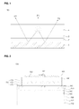
FIG. 1 is a conceptual view illustrating a light-emitting device according to one embodiment; -
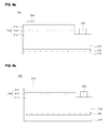
FIG. 2 is a sectional view illustrating a light-emitting device according to one embodiment; -
FIG. 3 is a sectional view illustrating the light-emitting device according to another embodiment; -
FIG. 4 is a sectional view illustrating the light-emitting device according to another embodiment; -
FIG. 5A is a sectional view illustrating the light-emitting device according to another embodiment; -
FIG. 5B is a sectional view illustrating the light-emitting device according to another embodiment; -
FIG. 6A is a sectional view illustrating the light-emitting device according to another embodiment; -
FIG. 6B is a sectional view illustrating the light-emitting device according to another embodiment; -
FIG. 6C is a sectional view illustrating the light-emitting device according to another embodiment; -
FIGS. 7 to 14 are views illustrating a series of processes for manufacturing the light-emitting device according to another embodiment; -
FIG. 15A is a perspective view illustrating a light-emitting device including the light-emitting device packages according to another embodiment; -
FIG. 15B is a sectional view illustrating a light-emitting device including the light-emitting device package according to another embodiment; and -
FIG. 15C is a sectional view illustrating a light-emitting device including the light-emitting device package according to another embodiment; -
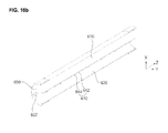
FIG. 16A is a perspective view illustrating a lighting device including the light-emitting device package according to another embodiment; -
FIG. 16B is a sectional view illustrating a lighting device including the light-emitting device package according to another embodiment; -
FIG. 17 is an exploded perspective view illustrating a liquid crystal display including the light-emitting device according to another embodiment; and -
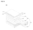
FIG. 18 is an exploded perspective view illustrating a liquid crystal display including the light-emitting device according to another embodiment. - Reference will now be made in detail to the embodiments of the present invention, examples of which are illustrated in the accompanying drawings. Wherever possible, the same reference numbers will be used throughout the drawings to refer to the same or like parts.
- Prior to description of the embodiments, it will be understood that, when an element such as a layer (film), region, pattern, or structure is referred to as being formed "on" or "under" another element, such as a substrate, layer (film), region, pad, or pattern, it can be directly "on" or "under" the other element or be indirectly formed with intervening elements therebetween. Further, "on" or "under" of each layer will be described based on illustration in the drawings.
- In the drawings, the thicknesses or sizes of respective layers are exaggerated, omitted or schematically illustrated for clarity and convenience of description. Therefore, the sizes of respective elements do not wholly reflect actual sizes thereof.
- Hereinafter, the present embodiments will be described with reference to the annexed drawings in more detail.
-
FIG. 1 is a concept view illustrating a light-emitting device according to one embodiment. - Referring to
FIG. 1 , the light-emittingdevice 10 according to the present embodiments include asupport member 1, areflective layer 2 arranged on thesupport member 1, aluminescence layer 3 arranged on thereflective layer 2 and a light-emittingstructure 4 arranged on theluminescence layer 3. - Among light emitted from the light-emitting
structure 4, direct light travelling in a direction P1 to directly discharge to the outside, but indirect light travelling in directions P2 and P3 passes through theluminescence layer 3 and is thus excited by a phosphor present in theluminescence layer 3, when it is reflected by thereflective layer 2 and directs to the outside or to thereflective layer 2. - Accordingly, the light-emitting device does not require an additional phosphor, other than the phosphor present in the
luminescence layer 3 and an additional luminescence layer is not formed in the light-emitting device package process, thus solving the problems of the package process. For example, the problem in which a sealant is deteriorated due to a phosphor formed in the sealant surrounding the light-emittingdevice 10 can be solved - Meanwhile, a ratio of light directly emitted from the light-emitting
structure 4 to the outside in a direction (P1) and light travelling toward thereflective layer 2 in directions (P2, P3) is about 1:2. - In this embodiment, the ratio of P1 : (P2 + P3) is 1 : 2. However, this ratio is a variable which may increase or decrease, depending on the structure of the light-emitting
structure 4 and it is apparent that the ratio is not limited thereto. - Meanwhile, as mentioned below, this embodiment may be applied to all of vertical light-emitting devices, horizontal light-emitting devices and flip chips, without being limited thereto.
-
FIG. 2 is a sectional view illustrating a light-emitting device according to a first embodiment. - Referring to
FIG. 2 , the light-emittingdevice 100 according to the first embodiment includes asupport member 110, a reflective layer arranged on thesupport member 110, aluminescence layer 140 arranged on thereflective layer 130, a first light-transmitting electrode layer 106 arranged on theluminescence layer 140, and a light-emittingstructure 170 arranged on the first light-transmittingelectrode layer 150. - The
support member 110 may be made of a thermally conductive material and may be a conductive support substrate composed of a conductive material such as a metal or conductive ceramic. Thesupport member 110 may be a mono-layer, or a di- or multi-layer including a metal layer (not shown) and an insulating layer (not shown). - That is, the
support member 110 may be made of a metal selected from Au, Ni, W, Mo, Cu, Al, Ta, Ag, Pt and Cr, or an alloy thereof. In addition, thesupport member 110 may be realized as a carrier wafer such as Si, Ge, GaAs, ZnO, SiC, SiGe, GaN or Ga2O3. - Such a
support member 110 facilitates discharge of light emitted from the light-emittingdevice 100 and thus improves thermal stability of the light-emittingdevice 100. - An
adhesive layer 112 may be laminated on thesupport member 110 and is made of a metal which exhibits superior adhesivity to a material arranged thereunder. - The
adhesive layer 112 includes, but is not limited to a barrier metal or a bonding metal and, for example, includes at least one of titanium (Ti), gold (Au), tin (Sn), nickel (Ni), chrome (Cr), gallium (Ga), indium (In), bismuth (Bi), copper (Cu), silver (Ag) and tantalum (Ta). Theadhesive layer 112 may be formed by joining different adhesive layers (not shown), without being limited thereto. - Meanwhile, the
adhesive layer 112 may further include adiffusion barrier layer 120. Accordingly, theadhesive layer 112 and thediffusion barrier layer 120 may be integrated in a mono-layer, or thediffusion barrier layer 120 is arranged on or under theadhesive layer 112 such that these layers are separated from each other. The configuration and lamination order of theadhesive layer 112 and thediffusion barrier layer 120 are not limited. - Meanwhile, at least one of the
adhesive layer 112 and thediffusion barrier layer 120 is formed on thesupport member 110, although the present invention is not limited thereto. - A
reflective layer 130 may be arranged on thediffusion barrier layer 120. - The
reflective layer 130 may be interposed between thesupport member 110 and theluminescence layer 140 and is composed of a highly reflective material selected from Ag, Ni, Al, Rh, Pd, Ir, Ru, Mg, Zn, Pt, Au, Hf and a combination thereof, may be a multi-layer formed using the metal material and a light-transmitting material such as IZO, IZTO, IAZO, IGZO, IGTO, AZO and ATO. Meanwhile, thereflective layer 130 may be a distributed Bragg reflector (DBR) formed by laminating a plurality of layers with different indexes of refraction and is not limited thereto. In addition, thereflective layer 130 may be a laminate of IZO/Ni, AZO/Ag, IZO/Ag/Ni, AZO/Ag/Ni or the like. Meanwhile, thereflective layer 130 may include any structure such as a roughness structure or a patterned structure and have a photonic crystal structure, without being limited thereto. - A
luminescence layer 140 may be arranged on thereflective layer 130. - A phosphor may be present in the
luminescence layer 140 and may be at least one of blue light-emitting phosphors, bluish green light-emitting phosphors, green light-emitting phosphors, yellowish green light-emitting phosphors, yellow light-emitting phosphors, yellowish red light-emitting phosphors, orange light-emitting phosphors, and red light-emitting phosphors, without being limited thereto. - That is, a phosphor is excited by a first light emitted from the light-emitting
device 100 to produce second light. For example, in the case where the light-emittingdevice 100 is a blue light-emitting diode and the phosphor is a yellow phosphor, the yellow phosphor is excited by blue light to emit yellow light, blue light emitted from the blue light-emitting diode is mixed with yellow light excited by blue light to allow the light-emittingdevice 100 to render white light. - Similarly, in the case where the light-emitting
device 100 is a green light-emitting diode, the magenta phosphor or a combination of blue and red phosphors may be exemplified, and in the case where the light-emittingdevice 100 is a red light-emitting diode, a cyan phosphor or a combination of blue and green phosphors may be exemplified. - Such a phosphor may be a known phosphor such as YAG, TAG, sulfides, silicates, aluminates, nitrides, carbides, nitridosililcates, borates, fluorides and phosphates.
- Preferably, in the case where the light-emitting
structure 170 emits ultraviolet light, theluminescence layer 140 may include all of R, G and B phosphors. R, G and B phosphors may be asingle luminescence layer 140 formed by separately laminating an R luminescence layer, a G luminescence layer and a B luminescence layer, or the R, G and B phosphors may be distributed in asingle luminescence layer 140. - The
luminescence layer 140 may be formed by thinly coating these phosphors, followed by sputtering, or nano-ink printing, without being limited thereto. In addition, aluminescence layer 140 may be formed by forming a layer composed of an epoxy, silicone or other resin material, dispersing a phosphor thereon and curing the same through heat or ultraviolet irradiation, without being limited thereto. - The
luminescence layer 140 enables light emitted from the light-emittingstructure 170 to render white-like color. However, light which directly emitted from the light-emittingstructure 170 to the outside may be blue, and the light-emittingdevice 100 according to this embodiment outputs bluish white light, which has slightly higher color temperature than conventional white light. - Meanwhile, a ratio of light which is directly emitted from the light-emitting
structure 170 to the outside in a direction (P1) and light which travels toward thereflective layer 2 in directions (P2, P3) is about 1:2. Accordingly, light emitted from the light-emittingdevice 100 according to the present embodiment may be white-like color. The color temperature of the white light may be changed, depending on the ratio of blue light, and the light-emittingdevice 100 according to this embodiment outputs bluish white light, that is, white light having a high color temperature. - In addition, as mentioned above, the ratio of P1 : (P2 + P3) is defined as 1 : 2. However, this ratio is a variable which may increase or decrease, depending on the structure of the light-emitting
structure 170 and it is apparent that the ratio is not limited thereto. - The
luminescence layer 140 excites first color light generated from the light-emittingstructure 170 to produce second color light. When theluminescence layer 140 is excessively thin, optical properties thereof may be deteriorated, and when theluminescence layer 140 is excessively thick, brightness may be reduced. Accordingly, theluminescence layer 140 may have a thickness range of 0.5 µm to 4 µm and preferably, of 1 µm to 2 µm. - The light-transmitting
electrode layer 150 may be arranged on theluminescence layer 140. - The light-transmitting
electrode layer 150 may be composed of at least one selected from ITO, IZO(In-ZnO), GZO(Ga-ZnO), AZO(Al-ZnO), AGZO(Al-Ga ZnO), IGZO(ln-Ga ZnO), IrOx, RuOx, RuOx/ITO, Ni/IrOx/Au and Ni/IrOx/Au/ITO, and is partially or entirely formed on the bottom of the light-emittingstructure 170 to prevent current crowding. - A current blocking layer (CBL, 160) may be arranged between the light-transmitting
electrode layer 150 and the light-emittingstructure 170. Thecurrent blocking layer 160 prevents current crowding in which current is concentrated on the bottom of theelectrode 184. Thecurrent blocking layer 160 may be composed of silicon dioxide (SiO2) or aluminum oxide (Al2O3) containing silicon dioxide (SiO2). - The light-emitting
structure 170 including a firstconductive semiconductor layer 171, anactive layer 172 and a secondconductive semiconductor layer 173 may be formed on the light-transmittingelectrode layer 150. - The first
conductive semiconductor layer 171 may be formed on the light-transmittingelectrode layer 150. The firstconductive semiconductor layer 171 may be realized with a p-type semiconductor layer doped with a p-type dopant. The p-type semiconductor layer may be selected from semiconductor materials such as GaN, AIN, AlGaN, InGaN, InN, InAlGaN and AllnN having the formula of InxAlyGa1-x-yN (0≤x≤1, 0 ≤y≤1, 0≤x+y≤1) and may be doped with a p-type dopant such as Mg, Zn, Ca, Sr and Ba. - The
active layer 172 is arranged on thefirst semiconductor layer 171. Theactive layer 172 may be formed with a mono or multi-quantum well structure, a quantum wire structure, a quantum dot structure or the like using a compound semiconductor material composed of Group III-V elements. - In the case where the
active layer 172 has a quantum well structure, for example, it may have a mono- or multi-quantum well structure including a well layer having the formula of InxAlyGa1-x-yN (0≤x≤1, 0 ≤y≤1, 0≤x+y≤1) and a barrier layer having the formula of InaAlbGa1-a-bN (0≤a≤1, 0 ≤b≤1, 0≤a+b≤1). The well layer may be formed of a material having a smaller band gap than that of the barrier layer. - A conductive clad layer (not shown) may be arranged on and/or under the
active layer 172. The conductive clad layer (not shown) may be composed of an AlGaN-based semiconductor, and may have a higher band gap than theactive layer 172. - The second
conductive semiconductor layer 173 may be formed on theactive layer 172. The secondconductive semiconductor layer 173 may be realized with an n-type semiconductor layer, and for example, the n-type semiconductor layer may be selected from semiconductor materials having the formula of InxAlyGa1-x-yN (0≤x≤1, 0 ≤y≤1, 0≤x+y≤1) such as GaN, AIN, AlGaN, InGaN, InN, InAlGaN and AlInN, and may be doped with an n-type dopant such as Si, Ge, Sn, Se and Te. - The
first semiconductor layer 171, theactive layer 172 and thesecond semiconductor layer 173 may be formed by a method such as metal organic chemical vapor deposition (MOCVD), chemical vapor deposition (CVD), plasma-enhanced chemical vapor deposition (PECVD), molecular beam epitaxy (MBE) and hydride vapor phase epitaxy (HVPE), without being limited thereto. - In addition, the concentration of conductive dopant doped in the
first semiconductor layer 171 and thesecond semiconductor layer 173 may be uniform or non-uniform. That is, the structure of a plurality of semiconductor layers may be varied and is not limited. - Meanwhile, the light-emitting
structure 170 may include a third semiconductor layer (not shown) with a polarity opposite that of thefirst semiconductor layer 171, arranged under thefirst semiconductor layer 171. In addition, thefirst semiconductor layer 171 may be realized with a p-type semiconductor layer and thesecond semiconductor layer 173 may be realized with an n-type semiconductor layer. Accordingly, the light-emittingstructure layer 170 may include at least one of N-P junction, P-N junction, N-P-N junction and P-N-P junction structures, without being limited thereto. - The second light-transmitting
electrode layer 180 may be formed on the secondconductive semiconductor layer 173. - The second light-transmitting
electrode layer 180 may be composed of the same material as the first light-transmittingelectrode layer 150 and is not limited thereto. - An
electrode 184 and alight extraction structure 182 are formed on the second light-transmittingelectrode layer 150. - The
electrode 184 may be formed in a mono- or multi-layer using a conductive material, for example, a metal selected from In, Co, Si, Ge, Au, Pd, Pt, Ru, Re, Mg, Zn, Hf, Ta, Rh, Ir, W, Ti, Ag, Cr, Mo, Nb, Al, Ni, Cu and WTi, or an alloy thereof. - The
light extraction structure 182 may be formed on the second light-transmittingelectrode layer 180 to uniformly disperse light from theactive layer 172 to the outside. Thelight extraction structure 182 may take the shape of a regular prism or an irregular pattern or may take the shape of a convex or concave lens, and may have another shape. Thelight extraction structure 182 may have a height of about 0.1 µm to about 3 µm and is irregular with a random size, without being limited thereto. Thelight extraction structure 182 may have an uneven upper surface which includes at least one selected from a textured pattern, a roughness pattern and an uneven pattern. - The side cross-section of the
light extraction structure 182 may have various shapes, such as a cylinder, a polyprism, a cone, a polypyramid, a circular truncated cone and a frustum of a pyramid, and preferably has a conical or polypyramidal shape. - A
passivation layer 190 may be formed on both sides of the light-emittingstructure 170 to prevent damage of the light-emittingstructure 170. - In
FIG. 2 , a part of light emitted from the light-emittingstructure 170 is discharged to the outside and the remaining light passes through the first light-transmittingelectrode layer 150 and travels towards thereflective layer 130. The ratio of light which is directly emitted from the light-emittingstructure 170 to the outside in a direction (P1) and light which travels toward thereflective layer 130 in directions (P2, P3) is about 1:2 to 1:3. White light can be realized through theluminescence layer 140 arranged under the light-emittingstructure 170 at this ratio. - Hereinafter, assuming that the light-emitting
structure 170 emits blue light, theluminescence layer 140 will be described. - Indirect light emitted from the light-emitting
structure 170 passes through theluminescence layer 140 and is excited by the phosphor arranged in theluminescence layer 140. Accordingly, blue indirect light is excited by the phosphor to produce white light. Meanwhile, when indirect light is reflected by thereflective layer 130 and travels toward the light-emittingstructure 170, it passes through theluminescence layer 140. Clearly, the indirect light reflected by thereflective layer 130 is also excited by the phosphor in theluminescence layer 140 to produce white light. - The
luminescence layer 140 and thereflective layer 130 are formed in the light-emittingdevice 100, light emitted from the light-emittingdevice 100 produces white light through theluminescence layer 140 and thereflective layer 130 present in the light-emittingdevice 100, thus eliminating the necessity of additional phosphor and causing no formation of theluminescence layer 140 in the light-emitting device package process and thereby solving problems involved in the package process. In addition, the necessity of forming the phosphor in a sealant formed in the light-emitting device package and surrounding the light-emittingdevice 100 is eliminated and problems associated with sealant deterioration can be solved. -
FIG. 3 is a sectional view illustrating the light-emitting device according to a second embodiment. - Referring to
FIG. 3 , the light-emittingdevice 100 according to this embodiment may include aluminescence layer 140 including apattern structure 142. - The
luminescence layer 140 may include apattern structure 142 which is patterned by a predetermined distance to provide a plurality of holes. Thepattern structure 142 may include with a plurality of holes which are spaced from one another by a predetermined or any distance, without being limited thereto. - The
luminescence layer 140 includes thepattern structure 142, thus preventing isolation between the light-emittingstructure 170 and the layer arranged therebelow. This increases current diffusion effects of the light-emittingstructure 170. - In addition, the
luminescence layer 140 includes thepattern structure 142, thus enabling indirect light which travels from the light-emittingstructure 170 toward thereflective layer 130 to produce blue-like color. - This behavior is due to the fact that, when indirect light is reflected from the
reflective layer 130 and passes to the outside, the percentage of the indirect light which passes through theluminescence layer 140 decreases. This means that the color temperature of light emitted from the light-emittingdevice 100 according to the second embodiment can be controlled depending on the width of the pattern formed on theluminescence layer 140. Blue light increases the color temperature while red light decreases the color temperature. - The
pattern structure 142 may have a patterning distance of 0.1 µm to 1 µm, and the patterning distance may increase or decrease depending on the thickness of theluminescence layer 140 and ease of manufacture, without being limited thereto. -
FIG. 4 is a sectional view illustrating the light-emitting device according to a third embodiment. - Referring to
FIG. 4 , the light-emittingdevice 100 according to the present embodiment may include aluminescence layer 140 including a plurality of layers. - The
luminescence layer 140 may include at least two layers, without being limited thereto. Preferably, respective layers may include at least one type of phosphor. For example, thefirst layer 141 includes an R phosphor, thesecond layer 142 includes a G phosphor, and thethird layer 143 includes a B phosphor, without being limited thereto. - The
luminescence layer 140 includes a plurality of layers and the respective layers include at least one type of phosphor, thus enabling the phosphor present in theluminescence layer 140 to be uniformly distributed and improving light distribution of the light-emittingdevice 100. - Meanwhile, the
first layer 141, thesecond layer 142 and thethird layer 143 have different indexes of refraction. - The
first layer 141, thesecond layer 142 and thethird layer 143 have different indexes of refraction, thus preventing total internal reflection, which may occur when indirect light emitted from the light-emittingstructure 170 passes through the respective layers, and thus improving light extraction efficiency of the light-emittingdevice 100. - Meanwhile, the
first layer 141, thesecond layer 142 and thethird layer 143 may include roughness (not shown). - The roughness (not shown) may be formed on at least one of the
first layer 141, thesecond layer 142 and thethird layer 143 and is not limited thereto. In addition, the cross-section of the roughness (not shown) may have various shapes, such as a cylinder, a polyprism, a cone, a polypyramid, a circular truncated cone, a frustum of a pyramid and a sphere, and is not limited thereto. - The
first layer 141, thesecond layer 142 and thethird layer 143 include a roughness (not shown), thus preventing total internal reflection which may occur when indirect light emitted from the light-emittingstructure 170 passes though the respective layers, and thereby improving light extraction efficiency of the light-emittingdevice 100. -
FIGS. 5A and 5B are sectional views illustrating the light-emitting device according to a fourth embodiment. - Referring to
FIG. 5A , thereflective layer 130 may include aroughness structure 131. - The
roughness structure 131 may be a regular or irregular pattern, may take the shape of a convex or concave lens, or may have another shape. - The side cross-section of the
roughness structure 131 may have various shapes, such as a cylinder, a polyprism, a cone, a polypyramid, a circular truncated cone and a frustum of a pyramid, without being limited thereto. - Meanwhile, referring to
FIG. 5B , thereflective layer 130 may be a distributed Bragg reflector (DBR) layer including a plurality of layers with different indexes of refraction. - The reflective layer 161 may include a
first layer 132 having a first index of refraction and asecond layer 134 having a second index of refraction different from the first refraction index. The first andsecond layers FIG. 5B , but are not limited thereto. Thereflective layer 130 may include a plurality of layers (not shown) having different indexes of refraction. - That is, the
reflective layer 130 has a structure in which thelayers first layer 132 may have a low index of refraction and thesecond layer 134 may have a high index of refraction, but the present invention is not limited thereto. - Meanwhile, assuming that A is a wavelength of light generated from the
active layer 172, n is an index of refraction of a medium and m is an odd number, thereflective layer 130 may have a laminate structure which may be obtained by repeatedly alternately laminating afirst layer 132 having a thickness of mλ/4n and a low index of refraction and asecond layer 134 having a high index of refraction to obtain a light reflectivity of 95% or higher in a specific wavelength region (A). - Accordingly, the
first layer 132 having a low index of refraction and thesecond layer 134 having a high index of refraction may have a thickness of λ/4 of reference wavelength and thelayers - In addition, the
layers reflective layer 130 may include Al2O3, SiO2, TiO2, TiNx, InOx, SiNx or TaxOy (x, y: constant), or include MxOy (M: metal, O: oxide, x, y: constant), but the present invention is not limited thereto. - In an example, the
first layer 132 having a low index of refraction may utilize SiO2 having an index of refraction of 1.4 or Al2O3 having an index of refraction of 1.6, thesecond layer 134 having a high index of refraction may utilize TiO2 having an index of refraction of 2 or higher, but the present invention is not limited thereto. - Meanwhile, the index of refraction of the medium between the
first layer 132 having a low index of refraction and thesecond layer 134 having a high index of refraction is increased in order to improve reflectivity, without being limited thereto. - Since the
reflective layer 130 has a larger band gap than that of oscillating wavelength, it does not absorb light and may realize high light reflectivity. -
FIGS. 6A to 6C are sectional views illustrating the light-emitting device according to a fifth embodiment. - Referring to
FIGS. 6A to 6C , the light-emittingdevice 200 according to this embodiment may include areflective layer 210, aluminescence layer 220 arranged on thereflective layer 210, asupport member 230 arranged on theluminescence layer 220, and a light-emittingstructure 240 arranged on thesupport member 230, the light-emittingstructure 240 including a firstconductive semiconductor layer 242, anactive layer 244 and a secondconductive semiconductor layer 246. - The
reflective layer 210 and theluminescence layer 220 have been described above and a detailed explanation thereof is thus omitted. - The
support member 230 is composed of a light transmitting material and may be a hetero-substrate such as sapphire (Al2O3) different from the semiconductor layer or a homo-substrate such as GaN which is the same as the semiconductor layer. In addition, thesupport member 230 may be a SiC substrate which has higher thermal conductivity than the sapphire (Al2O3) substrate and is not limited thereto. - Although not shown, a buffer layer (not shown) may be arranged on the
support member 230, to reduce lattice mismatch between thesupport member 230 and the firstconductive semiconductor layer 242 and facilitate growth of the semiconductor layers. - The buffer layer (not shown) may have an AlInN/GaN laminate structure, an InxGa1-xN/GaN laminate structure or an AlxInyGa1-x-yN/InxGa1-xN/GaN laminate structure which includes AIN and GaN.
- The light-emitting
structure 240 is arranged on thesupport member 230 and the light-emittingstructure 240 may include thefirst semiconductor layer 242, theactive layer 244 and thesecond semiconductor layer 246. - For example, the first
conductive semiconductor layer 242 may be an n-type semiconductor layer and the secondconductive semiconductor layer 246 may be a p-type semiconductor layer, without being limited thereto. Meanwhile, respective n-type semiconductor layers and p-type semiconductor layers have been described above and a detailed explanation thereof is thus omitted. - An
first electrode 252 may be formed on thefirst semiconductor layer 242, and asecond electrode 254 may be formed on thesecond semiconductor layer 246. - Some regions of the
first semiconductor layer 242 are exposed by removing some regions of theactive layer 244 and thesecond semiconductor layer 246, and thefirst electrode 252 is formed on the upper surface of thefirst semiconductor layer 242 in the exposed region. That is, thefist semiconductor layer 242 is provided with the upper surface facing theactive layer 244 and the lower surface facing thesupport member 230, the upper surface of thefirst semiconductor layer 242 includes the exposed regions, and thefirst electrode 252 is disposed in the exposed regions of the upper surface of thefirst semiconductor layer 242. - Exposure of some regions of the
first semiconductor layer 242 may be carried out using a specific etching method, but is not limited thereto. As the etching method, the wet etching method or the dry etching method may be used. - The first and
second electrode second electrode - Meanwhile, as shown in
FIG. 6A , thesupport member 230 may be arranged on theluminescence layer 220, or, as shown inFIG. 6B , thesupport member 230 surrounds theluminescence layer 220, or, as shown inFIG. 6C , thesupport member 230 surrounds theluminescence layer 220 and thereflective layer 210, without being limited thereto. - The
support member 230 surrounds theluminescence layer 220, thereflective layer 210, or theluminescence layer 220, to secure reliable connection between thesupport member 230, theluminescence layer 220 and thereflective layer 210. - As shown in
FIGS. 6A and 6B , the light-emittingdevice 200 according to the embodiment may be a vertical light-emitting device, a horizontal light-emitting device or a flip chip, without being limited thereto. -
FIGS. 7 to 14 are views illustrating a series of processes for manufacturing the light-emitting device according to one embodiment. - First, as shown in
FIG. 7 , a light-emittingstructure 320 including a first conductive semiconductor layer, an active layer and a second conductive semiconductor layer is formed on afirst support member 310, and acurrent blocking layer 330 is formed on the light-emittingstructure 320. Thefirst support member 310 may be a sapphire substrate, but is not limited thereto. Then, a light-transmittingelectrode layer 340 is formed on the light-emittingstructure 320 including thecurrent blocking layer 330. At this time, it is assumed that the light-emittingstructure 320 emits blue light. - Then, as shown in
FIG. 8 , aluminescence layer 350 is formed on the light-transmittingelectrode layer 340. Theluminescence layer 350 has a thickness of 1 µm to 2 µm. Meanwhile, after theluminescence layer 350 is formed, it may be further subjected to a patterning process. - Then, as shown in
FIG. 9 , areflective layer 360 is formed on theluminescence layer 350, and, as shown inFIG. 10 , adiffusion barrier layer 370 and anadhesive layer 380 are sequentially formed thereon. - Then, as shown in
FIG. 11 , asecond support member 390 is adhered to theadhesive layer 380. The process ofFIG. 11 is a process for forming a sub-support member to replace thefirst support member 310, before thefirst support member 310 is removed. - Then, as shown in
FIG. 12 , thefirst support member 310 is removed. The process of removing thefirst support member 310 may be an LLO process. The LLO process is carried out by irradiating a laser with a wavelength range of 300 nm to 400 nm to the boundary between thefirst support member 310 and the light-emittingstructure 320, and separating thefirst support member 310 from the light-emittingstructure 320. When thefirst support member 310 is removed by the LLO process illustrated inFIG. 12 , thesecond support member 390 may replace thefirst support member 310, as shown inFIG. 13 . Meanwhile, in order to protect an exposed region of the light-emittingstructure 320, apassivation layer 395 is formed at both sides of the light-emitting structure through a passivation process. - Finally, a
light extraction structure 322 is formed on the light-emittingstructure 320 illustrated inFIG. 14 and anelectrode 324 is formed thereon. Meanwhile, as shown inFIG. 2 , alight extraction structure 322 may be formed on a second light-transmitting electrode layer (not shown) provided on the surface of the light-emittingstructure 320, but is not limited thereto. -
FIGS. 15A to 15C are a perspective view and a sectional view illustrating a light-emitting device package according to one embodiment. - Referring to
FIGS. 15A to 15C , a light-emittingdevice package 500 includes abody 510 including acavity 520, first and second lead frames 540 and 550 mounted on thebody 510, a light-emittingdevice 530 electrically connected to the first and secondlead frame cavity 520 to cover the light-emittingdevice 530. - The
body 510 may be composed of at least one selected from resin materials such as polyphthalamide (PPA), silicon (Si), aluminum (Al), aluminum nitride (AIN), photo sensitive glass (PSG), polyamide9T (PA9T), syndiotactic polystyrene (SPS), metal materials, sapphire (Al2O3), beryllium oxide (BeO) and printed circuit boards (PCB). Thebody 510 may be formed by a process such as injection molding and etching, without being limited thereto. - The inner surface of the
body 510 may include an inclined surface. The reflective angle of light emitted from the light-emittingdevice 530 may be varied depending on the angle of the inclined surface. Accordingly, the orientation angle of light discharged outside can be controlled. - As the orientation angle of light decreases, convergence of light emitted from the light-emitting
device 530 to the outside increases. On the other hand, as the orientation angle of light increases, convergence of light from the light-emittingdevice 530 to the outside decreases. - Meanwhile, as seen from the top, the
cavity 520 provided in thebody 510 may have various shapes including a circular shape, a rectangular shape, a polygonal shape, an oval shape and a shape with curved corners, although the present invention is not limited thereto. - The light-emitting
device 530 may be electrically connected to the first and second lead frames 540 and 550 in a flip chip manner. - Meanwhile, the light-emitting
device 530 according to this embodiment includes a reflective layer (not shown) to improve luminous efficiency. - The
cavity 520 is filled with the sealant (not shown) such that the sealant covers the light-emittingdevice 530. - The sealant (not shown) may be composed of silicon, epoxy or other resin material and may be formed by filling the
cavity 520 with a sealant material, followed by UV or heat curing. - In addition, the sealant (not shown) may include a phosphor, and the phosphor is selected from depending on the wavelength of light emitted from the light-emitting
device 530 to allow the light-emitting device package to render white light. - Meanwhile, since the light-emitting
device 530 according to one embodiment includes a luminescence layer (not shown) and a reflective layer (not shown), the phosphor may be not present in the sealant (not shown) and problems generated in the light-emitting device packaging process may be thus prevented. - The first and second lead frames 540 and 550 may include a metal material selected from titanium (Ti), copper (Cu), nickel (Ni), gold (Au), chrome (Cr), tantalum (Ta), platinum (Pt), tin (Sn), silver (Ag), phosphorus (P), aluminum (Al), indium (In), palladium (Pd), cobalt (Co), silicon (Si), germanium (Ge), hafnium (Hf), ruthenium (Ru), iron (Fe), and an alloy thereof. In addition, the first and second lead frames 540 and 550 may have a mono- or multi-layer structure, although the present invention is not limited thereto.
- The first
second lead frame device 530 is mounted on the first and second lead frames 540 and 550, and the first and second lead frames 540 and 550 directly contact the light-emittingdevice 530, or are electrically connected thereto through a conductive material such as soldering member (not shown). In addition, the light-emittingdevice 530 may be electrically connected to the first and second lead frames 540 and 550 via wire bonding, although the present invention is not limited thereto. Accordingly, when a power source is connected to the first and second lead frames 540 and 550, power may be supplied to the light-emittingdevice 530. Meanwhile, a plurality of lead frames (not shown) are mounted in thebody 510 and respective lead frames (not shown) are electrically connected to the light-emittingdevice 530, although the present invention is not limited thereto. - Meanwhile, referring to
FIG. 15C , the light-emittingdevice package 500 according to the embodiment may include an optical sheet 580 and the optical sheet 580 may include abase 582 and a prism pattern 584. - The
base 582 is a supporter to form the prism pattern 584, which is composed of a transparent material exhibiting superior thermal stability. For example, such a transparent material may be selected from the group consisting of polyethylene terephthalate, polycarbonate, polypropylene, polyethylene, polystyrene and polyepoxy, but is not limited thereto. - In addition, the
base 582 may include a phosphor (not shown). For example, thebase 582 may be formed by homogenously dispersing a phosphor (not shown) in the material constituting thebase 582, followed by curing. When thebase 582 is formed according to this method, the phosphor (not shown) can be homogeneously dispersed throughout thebase 582. - Meanwhile, a prism pattern 584 to refract and concentrate light may be arranged on the
base 582. A material for the prism pattern 584 may be an acrylic resin, without being limited thereto. - The prism pattern 584 includes a plurality of linear prisms arranged in one direction on one surface of the base 582 such that the linear prisms are parallel to one another and the cross-section of the linear prisms taken along an axial direction may take the shape of a triangle.
- The prism pattern 584 can concentrate light. For this reason, when the optical sheet 580 is adhered to the light-emitting
device package 500 ofFIG. 5 , straightness of light can be improved and brightness of the light-emittingdevice package 500 can be thus enhanced. - Meanwhile, the prism pattern 584 may include a phosphor (not shown).
- The phosphor (not shown) may be uniformly present in the prism pattern 584 by mixing the phosphor with an acrylic resin which forms the prism pattern 584 in a dispersed state to produce a paste or slurry and then forming the prism pattern 584.
- In the case where the phosphor (not shown) is present in the prism pattern 584, light uniformity and distribution level of the light-emitting
device package 500 are improved and the orientation angle of light-emittingdevice package 500 can be thus improved due to dispersion effect of light by the phosphor (not shown) as well as concentration effect of light by the prism pattern 584. - The light-emitting
device package 500 according to one embodiment is arrayed in plural on the substrate and optical members such as the light guide plate, prism sheet and diffusion sheet may be arranged on a light passage of the light-emittingdevice package 500. The light-emitting device package, the substrate and the optical members may serve as a light unit. In another embodiment, a display device, an indicating device and a lighting device including the light-emitting device or light-emitting device packages disclosed in the afore-mentioned embodiments may be realized. For example, the lighting device may include a lamp, a streetlamp, or the like. -
FIG. 16A is a perspective view illustrating a lighting device including the light-emitting device package according to one embodiment.FIG. 16B is a sectional view illustrating the cross-section taken along the line of C-C' of the lighting device ofFIG. 16A . - Referring to
FIGS. 16A and16B , thelighting device 600 may include abody 610, acover 630 connected to thebody 610 and anend cap 650 arranged at both ends of thebody 610. - A light-emitting
device module 640 is connected to the bottom of thebody 610 and thebody 610 may be composed of a metal material which exhibits superior conductivity and heat release effect in order to discharge heat generated from the light-emittingdevice package 644 to the outside through the top of thebody 610. - The light-emitting device packages 644 are mounted on the
PCB 642 in multiple colors and multiple rows to constitute an array, and may be spaced from one another by a predetermined distance or by different distances, as necessary, to control brightness. ThePCB 642 may be a metal core PCB (MPPCB) or PCB made of FR4. - In particular, each light-emitting
device package 644 includes a light-emitting device (not shown), and the light-emitting device (not shown) includes a reflective layer (not shown) to improve light extraction efficiency and thereby improve luminous efficiency of the light-emitting device package and lighting device. - The light-emitting
device package 644 includes an extended lead frame (not shown), thus improving light irradiation and thus enhance reliability and efficiency of the light-emittingdevice package 644, and lengthening the lifespan of thelighting device 600 including the light-emitting device package 622 and the light-emittingdevice package 644. - The
cover 630 may take the shape of a circle to surround the bottom of thebody 610, without being limited thereto. - The
cover 630 protects the light-emittingdevice module 640 from foreign substances. In addition, thecover 630 prevents glare generated from the light-emittingdevice package 644 and includes diffusion particles to uniformly discharge light to the outside. In addition, a prism pattern or the like may be formed on at least one of the inner and outer surfaces of thecover 630. Alternatively, a phosphor may be applied onto at least one of the inner and outer surfaces of thecover 630. - Meanwhile, the
cover 630 should exhibit superior light transmittance, so that it can discharge light generated from the light-emittingdevice package 644 through thecover 630 to the outside, and thecover 630 should exhibit sufficient heat resistance so that it can endure heat emitted by the light-emittingdevice package 644. Preferably, thecover 630 is composed of a material including polyethylene terephthalate (PET), polycarbonate (PC) or polymethyl methacrylate (PMMA) and the like. - The
end cap 650 is arranged on both ends of thebody 610 and may be used to seal a power device (not shown). In addition, theend cap 650 may include apower pin 652, allowing thelighting device 600 to be applied to a conventional terminal in which a fluorescent light is removed, without using any additional device. -
FIG. 17 is an exploded perspective view illustrating a liquid crystal display including the light-emitting device according to one embodiment. -
FIG. 17 illustrates an edge-light type liquidcrystal display device 700 which includes a liquidcrystal display panel 710 and abacklight unit 770 to supply light to the liquidcrystal display panel 710. - The liquid
crystal display panel 710 displays an image using light supplied from thebacklight unit 770. The liquidcrystal display panel 710 includes acolor filter substrate 712 and a thin film transistor substrate 714 which face each other such that a liquid crystal is interposed therebetween. - The
color filter substrate 712 can realize color of images to be displayed through the liquidcrystal display panel 710. - The thin film transistor substrate 714 is electrically connected to a printed
circuit board 718 on which a plurality of circuit components are mounted through a drivingfilm 717. The thin film transistor substrate 714 responds to drive signals supplied from the printedcircuit board 718 and may apply a drive voltage from the printedcircuit board 718 to liquid crystals. - The thin film transistor substrate 714 includes a thin film transistor and a pixel electrode formed as a thin film on another substrate composed of a transparent material such as glass or plastic.
- The
backlight unit 770 includes a light-emittingdevice module 720, a light guide plate 730 to convert light emitted from the light-emittingdevice module 720 into a surface light source and supply the light to the liquidcrystal display panel 710, a plurality offilms - The light-emitting
device module 720 includes a plurality of light-emitting device packages 724 and aPCB 722 on which the light-emitting device packages 724 are mounted to form an array. - In particular, the light-emitting
device package 724 includes a light-emitting device (not shown) and the light-emitting device (not shown) includes a reflective layer (not shown) to improve light extraction efficiency and thereby luminous efficiency of the light-emittingdevice package 724 and thebacklight unit 770. - Meanwhile, the
backlight unit 770 includes adiffusion film 766 to diffuse light incident from the light guide plate 730 toward the liquidcrystal display panel 710, aprism film 750 to concentrate the diffused light and thus improve vertical incidence and aprotective film 764 to protect theprism film 750. -
FIG. 18 is an exploded perspective view illustrating a liquid crystal display including the light-emitting device according to one embodiment. The contents illustrated and described inFIG. 17 are not mentioned in detail. -
FIG. 18 illustrates a direct-type liquidcrystal display device 800 which includes a liquidcrystal display panel 810 and abacklight unit 870 to supply light to the liquidcrystal display panel 810. - The liquid
crystal display panel 810 has been described inFIG. 7 and a detailed explanation thereof is omitted. - The
backlight unit 870 includes a plurality of light-emittingdevice modules 823, areflective sheet 824, alower chassis 830 in which the light-emittingdevice modules 823 and thereflective sheet 824 are accepted, adiffusion plate 840 arranged on the light-emittingdevice modules 823, and a plurality ofoptical films 860. - Each light-emitting
device module 823 includes a plurality of light-emitting device packages and aPCB 821 on which the light-emitting device packages 824 are mounted to form an array. - In particular, the light-emitting
device package 822 includes a light-emitting device (not shown) and the light-emitting device (not shown) includes a reflective layer (not shown) to improve light extraction efficiency and thereby luminous efficiency of the light-emitting device packages 824 and thebacklight unit 870. - The
reflective sheet 824 reflects light generated from light-emittingdevice package 822 toward the liquidcrystal display panel 810 to improve luminous efficacy. - Meanwhile, light emitted from the light-emitting
device module 823 is incident on thediffusion plate 840 and anoptical film 860 is arranged on thediffusion plate 840. Theoptical film 860 includes adiffusion film 866, aprism film 850 and aprotective film 864. - Although the embodiments of the present invention have been disclosed for illustrative purposes, those skilled in the art will appreciate that various modifications, additions and substitutions are possible, without departing from the scope and spirit of the invention as disclosed in the accompanying claims. For example, the respective elements described in detail in the embodiments may be modified. Further, it will be understood that differences relating to these modifications, additions and substitutions are covered by the scope of the invention defined in the accompanying claims.
Claims (15)
- A light-emitting device comprising:a reflective layer;a light-emitting structure on the reflective layer, the light-emitting structure including a first conductive semiconductor layer, an active layer and a second conductive semiconductor layer; anda luminescence layer interposed between the reflective layer and the light-transmitting electrode layer.
- The device according to claim 1, wherein the luminescence layer comprises at least one of yellow phosphors, YAG, TAG, sulfide, silicate, aluminate, nitride, carbide, nitridosililcate, borate, fluoride and phosphate phosphors, and R, G and B tri-color phosphors.
- The device according to claim 1, wherein the luminescence layer has a thickness of 0.5 µm to 4 µm.
- The device according to claim 1, wherein the luminescence layer has a thickness of 1 µm to 2 µm.
- The device according to claim 1, wherein the luminescence layer includes a pattern structure.
- The device according to claim 5, wherein the pattern structure includes pattern units spaced from one another by a predetermined distance of 0.1 µm to 1 µm.
- The device according to claim 1, wherein the luminescence layer comprises at least two layers.
- The device according to claim 7, wherein the luminescence layer comprises a first layer including an R phosphor, a second layer including a G phosphor, and a third layer including a B phosphor.
- The device according to claim 1, wherein the reflective layer comprises a first layer having a first index of refraction and a second layer having a second index of refraction,
wherein the second index of refraction is different from the first index of refraction. - The device according to claim 1, further comprising:a current blocking layer,wherein the current blocking layer is interposed between the light-transmitting electrode layer and the light-emitting structure.
- The device according to claim 10, wherein the current blocking layer comprises at least one of silicon dioxide (SiO2) or aluminum oxide (Al2O3).
- The device according to claim 1, further comprising:a support member; anda light-transmitting electrode layer,wherein the support member is arranged under the reflective layer and the light-transmitting electrode layer is interposed between the luminescence layer and the light-emitting structure.
- The device according to claim 1, further comprising:a support member,wherein the support member is arranged on the reflective layer.
- The device according to claim 13, wherein the support member surrounds the luminescence layer.
- The device according to claim 13, wherein the support member surrounds the luminescence layer and the reflective layer.
Applications Claiming Priority (1)
| Application Number | Priority Date | Filing Date | Title |
|---|---|---|---|
| KR1020100047587A KR101662010B1 (en) | 2010-05-20 | 2010-05-20 | Light Emitting Device |
Publications (3)
| Publication Number | Publication Date |
|---|---|
| EP2388839A2 true EP2388839A2 (en) | 2011-11-23 |
| EP2388839A3 EP2388839A3 (en) | 2015-11-25 |
| EP2388839B1 EP2388839B1 (en) | 2020-04-29 |
Family
ID=44546354
Family Applications (1)
| Application Number | Title | Priority Date | Filing Date |
|---|---|---|---|
| EP11166278.9A Active EP2388839B1 (en) | 2010-05-20 | 2011-05-16 | Light emitting device with wavelength conversion layer between a reflective layer and the light-emitting diode layers. |
Country Status (4)
| Country | Link |
|---|---|
| US (2) | US8779450B2 (en) |
| EP (1) | EP2388839B1 (en) |
| KR (1) | KR101662010B1 (en) |
| CN (1) | CN102255017B (en) |
Cited By (1)
| Publication number | Priority date | Publication date | Assignee | Title |
|---|---|---|---|---|
| EP2827391A1 (en) * | 2013-07-15 | 2015-01-21 | LG Innotek Co., Ltd. | Light emitting diode and light emitting diode package |
Families Citing this family (16)
| Publication number | Priority date | Publication date | Assignee | Title |
|---|---|---|---|---|
| JP4975130B2 (en) * | 2009-05-07 | 2012-07-11 | キヤノン株式会社 | Photonic crystal surface emitting laser |
| US10243121B2 (en) | 2011-06-24 | 2019-03-26 | Cree, Inc. | High voltage monolithic LED chip with improved reliability |
| KR101956066B1 (en) * | 2012-06-08 | 2019-03-11 | 엘지이노텍 주식회사 | Light emitting device, light emitting device package, and light unit |
| TWI499077B (en) * | 2012-12-04 | 2015-09-01 | High Power Opto Inc | Semiconductor light-emitting element |
| CN103367386A (en) * | 2013-07-10 | 2013-10-23 | 中国科学院半导体研究所 | Alternating-current light-emitting diode (LED) |
| TWI637534B (en) * | 2013-11-29 | 2018-10-01 | 晶元光電股份有限公司 | Illuminating device |
| CN104701433B (en) * | 2013-12-06 | 2019-04-16 | 晶元光电股份有限公司 | light-emitting device |
| JP2016054260A (en) * | 2014-09-04 | 2016-04-14 | 株式会社東芝 | Semiconductor light emitting device |
| JP2016062945A (en) * | 2014-09-16 | 2016-04-25 | 株式会社東芝 | Semiconductor light-emitting element and light-emitting device |
| US10658546B2 (en) * | 2015-01-21 | 2020-05-19 | Cree, Inc. | High efficiency LEDs and methods of manufacturing |
| KR20160124375A (en) * | 2015-04-17 | 2016-10-27 | 삼성전자주식회사 | Method of manufacturing semiconductor light emitting device package |
| KR101739851B1 (en) * | 2015-10-30 | 2017-05-25 | 주식회사 썬다이오드코리아 | Light emitting device comprising wavelength conversion structures |
| JP6870592B2 (en) * | 2017-11-24 | 2021-05-12 | 豊田合成株式会社 | Light emitting device |
| US10554018B2 (en) | 2017-12-19 | 2020-02-04 | International Business Machines Corporation | Hybrid vertical current injection electro-optical device with refractive-index-matched current blocking layer |
| CN114766065B (en) * | 2019-06-19 | 2025-06-24 | 上海显耀显示科技有限公司 | Systems and methods for multi-color LED pixel units |
| KR20230022942A (en) * | 2020-06-03 | 2023-02-16 | 제이드 버드 디스플레이(상하이) 리미티드 | Systems and Methods for Multicolor LED Pixel Unit with Vertical Light Emission |
Citations (1)
| Publication number | Priority date | Publication date | Assignee | Title |
|---|---|---|---|---|
| KR20100047587A (en) | 2008-10-29 | 2010-05-10 | 세메스 주식회사 | Shaft apparatus for conveying substrate |
Family Cites Families (17)
| Publication number | Priority date | Publication date | Assignee | Title |
|---|---|---|---|---|
| US6373188B1 (en) | 1998-12-22 | 2002-04-16 | Honeywell International Inc. | Efficient solid-state light emitting device with excited phosphors for producing a visible light output |
| JP2001177145A (en) * | 1999-12-21 | 2001-06-29 | Toshiba Electronic Engineering Corp | Semiconductor light emitting device and method of manufacturing the same |
| JP2002170989A (en) | 2000-12-04 | 2002-06-14 | Sharp Corp | Nitride compound semiconductor light emitting device |
| US6841802B2 (en) * | 2002-06-26 | 2005-01-11 | Oriol, Inc. | Thin film light emitting diode |
| DE102004052245A1 (en) * | 2004-06-30 | 2006-02-02 | Osram Opto Semiconductors Gmbh | Radiation emitting semiconductor chip e.g. luminescent diode chip, has reemission structure, and reemission layer formed for widening spectrums of chip against respective spectrum of radiation of peak wavelength |
| JP2006100500A (en) | 2004-09-29 | 2006-04-13 | Sanken Electric Co Ltd | Semiconductor light emitting device and manufacturing method thereof |
| KR100799859B1 (en) * | 2006-03-22 | 2008-01-31 | 삼성전기주식회사 | White light emitting device |
| US8080828B2 (en) | 2006-06-09 | 2011-12-20 | Philips Lumileds Lighting Company, Llc | Low profile side emitting LED with window layer and phosphor layer |
| DE102007003785A1 (en) * | 2007-01-19 | 2008-07-24 | Merck Patent Gmbh | Emitter converter chip |
| KR20080069074A (en) | 2007-01-22 | 2008-07-25 | 삼성에스디아이 주식회사 | Plasma display panel |
| TW200837978A (en) * | 2007-03-02 | 2008-09-16 | Yu-Nung Shen | Light-emitting diode chip package and packaging method thereof |
| CN101378103A (en) | 2007-08-28 | 2009-03-04 | 富士迈半导体精密工业(上海)有限公司 | White light light-emitting device and manufacturing method thereof |
| KR101393355B1 (en) * | 2007-12-28 | 2014-06-30 | 서울바이오시스 주식회사 | Light emitting diode and method of fabricating the same |
| KR101420214B1 (en) * | 2008-01-21 | 2014-07-17 | 엘지이노텍 주식회사 | The nitride-based light- |
| DE102008012407A1 (en) * | 2008-01-31 | 2009-08-06 | Osram Opto Semiconductors Gmbh | Radiation-emitting device |
| JP2010092957A (en) * | 2008-10-06 | 2010-04-22 | Panasonic Corp | Light emitting diode and method of manufacturing the same |
| CN201532968U (en) * | 2009-10-20 | 2010-07-21 | 厦门市三安光电科技有限公司 | White light-emitting diode chip |
-
2010
- 2010-05-20 KR KR1020100047587A patent/KR101662010B1/en not_active Expired - Fee Related
-
2011
- 2011-05-05 US US13/101,701 patent/US8779450B2/en active Active
- 2011-05-16 EP EP11166278.9A patent/EP2388839B1/en active Active
- 2011-05-20 CN CN201110136495.7A patent/CN102255017B/en active Active
-
2014
- 2014-06-16 US US14/305,756 patent/US9224926B2/en not_active Expired - Fee Related
Patent Citations (1)
| Publication number | Priority date | Publication date | Assignee | Title |
|---|---|---|---|---|
| KR20100047587A (en) | 2008-10-29 | 2010-05-10 | 세메스 주식회사 | Shaft apparatus for conveying substrate |
Cited By (3)
| Publication number | Priority date | Publication date | Assignee | Title |
|---|---|---|---|---|
| EP2827391A1 (en) * | 2013-07-15 | 2015-01-21 | LG Innotek Co., Ltd. | Light emitting diode and light emitting diode package |
| KR20150008576A (en) * | 2013-07-15 | 2015-01-23 | 엘지이노텍 주식회사 | Light emitting device and light emitting device package |
| US9627584B2 (en) | 2013-07-15 | 2017-04-18 | Lg Innotek Co., Ltd. | Light emitting device and light emitting device package |
Also Published As
| Publication number | Publication date |
|---|---|
| US9224926B2 (en) | 2015-12-29 |
| CN102255017B (en) | 2015-11-25 |
| US20110284896A1 (en) | 2011-11-24 |
| KR101662010B1 (en) | 2016-10-05 |
| US8779450B2 (en) | 2014-07-15 |
| CN102255017A (en) | 2011-11-23 |
| US20140339588A1 (en) | 2014-11-20 |
| KR20110128007A (en) | 2011-11-28 |
| EP2388839B1 (en) | 2020-04-29 |
| EP2388839A3 (en) | 2015-11-25 |
Similar Documents
| Publication | Publication Date | Title |
|---|---|---|
| EP2388839B1 (en) | Light emitting device with wavelength conversion layer between a reflective layer and the light-emitting diode layers. | |
| US8357949B2 (en) | Light-emitting device, light-emitting device package and lighting system | |
| US8669560B2 (en) | Light-emitting device, light-emitting device package and lighting system | |
| US10886436B2 (en) | Light-emitting device and lighting apparatus | |
| EP2581953B1 (en) | Light emitting device | |
| US9455371B2 (en) | Light emitting device | |
| US9070832B2 (en) | Light-emitting device and fabrication method thereof | |
| CN102214752B (en) | Light emitting device | |
| US8759853B2 (en) | Light emitting device | |
| US8426885B2 (en) | Light emitting device | |
| US8405093B2 (en) | Light emitting device | |
| KR20120072739A (en) | Light emitting device | |
| KR20130022621A (en) | Light emitting diode package | |
| KR20120104000A (en) | Light emitting device | |
| KR20140097604A (en) | Light emitting device | |
| KR20130036615A (en) | Light emitting diode package |
Legal Events
| Date | Code | Title | Description |
|---|---|---|---|
| 17P | Request for examination filed |
Effective date: 20110516 |
|
| AK | Designated contracting states |
Kind code of ref document: A2 Designated state(s): AL AT BE BG CH CY CZ DE DK EE ES FI FR GB GR HR HU IE IS IT LI LT LU LV MC MK MT NL NO PL PT RO RS SE SI SK SM TR |
|
| AX | Request for extension of the european patent |
Extension state: BA ME |
|
| PUAI | Public reference made under article 153(3) epc to a published international application that has entered the european phase |
Free format text: ORIGINAL CODE: 0009012 |
|
| RAP1 | Party data changed (applicant data changed or rights of an application transferred) |
Owner name: LG INNOTEK CO., LTD. |
|
| PUAL | Search report despatched |
Free format text: ORIGINAL CODE: 0009013 |
|
| AK | Designated contracting states |
Kind code of ref document: A3 Designated state(s): AL AT BE BG CH CY CZ DE DK EE ES FI FR GB GR HR HU IE IS IT LI LT LU LV MC MK MT NL NO PL PT RO RS SE SI SK SM TR |
|
| AX | Request for extension of the european patent |
Extension state: BA ME |
|
| RIC1 | Information provided on ipc code assigned before grant |
Ipc: H01L 33/50 20100101AFI20151021BHEP Ipc: H01L 33/08 20100101ALN20151021BHEP Ipc: H01L 33/46 20100101ALN20151021BHEP |
|
| RBV | Designated contracting states (corrected) |
Designated state(s): AL AT BE BG CH CY CZ DE DK EE ES FI FR GB GR HR HU IE IS IT LI LT LU LV MC MK MT NL NO PL PT RO RS SE SI SK SM TR |
|
| RAP1 | Party data changed (applicant data changed or rights of an application transferred) |
Owner name: LG INNOTEK CO., LTD. |
|
| STAA | Information on the status of an ep patent application or granted ep patent |
Free format text: STATUS: EXAMINATION IS IN PROGRESS |
|
| 17Q | First examination report despatched |
Effective date: 20190313 |
|
| GRAP | Despatch of communication of intention to grant a patent |
Free format text: ORIGINAL CODE: EPIDOSNIGR1 |
|
| STAA | Information on the status of an ep patent application or granted ep patent |
Free format text: STATUS: GRANT OF PATENT IS INTENDED |
|
| INTG | Intention to grant announced |
Effective date: 20191220 |
|
| GRAS | Grant fee paid |
Free format text: ORIGINAL CODE: EPIDOSNIGR3 |
|
| GRAJ | Information related to disapproval of communication of intention to grant by the applicant or resumption of examination proceedings by the epo deleted |
Free format text: ORIGINAL CODE: EPIDOSDIGR1 |
|
| GRAL | Information related to payment of fee for publishing/printing deleted |
Free format text: ORIGINAL CODE: EPIDOSDIGR3 |
|
| STAA | Information on the status of an ep patent application or granted ep patent |
Free format text: STATUS: EXAMINATION IS IN PROGRESS |
|
| GRAR | Information related to intention to grant a patent recorded |
Free format text: ORIGINAL CODE: EPIDOSNIGR71 |
|
| STAA | Information on the status of an ep patent application or granted ep patent |
Free format text: STATUS: GRANT OF PATENT IS INTENDED |
|
| GRAA | (expected) grant |
Free format text: ORIGINAL CODE: 0009210 |
|
| STAA | Information on the status of an ep patent application or granted ep patent |
Free format text: STATUS: THE PATENT HAS BEEN GRANTED |
|
| INTC | Intention to grant announced (deleted) | ||
| AK | Designated contracting states |
Kind code of ref document: B1 Designated state(s): AL AT BE BG CH CY CZ DE DK EE ES FI FR GB GR HR HU IE IS IT LI LT LU LV MC MK MT NL NO PL PT RO RS SE SI SK SM TR |
|
| INTG | Intention to grant announced |
Effective date: 20200324 |
|
| REG | Reference to a national code |
Ref country code: GB Ref legal event code: FG4D |
|
| REG | Reference to a national code |
Ref country code: CH Ref legal event code: EP |
|
| REG | Reference to a national code |
Ref country code: DE Ref legal event code: R096 Ref document number: 602011066485 Country of ref document: DE |
|
| REG | Reference to a national code |
Ref country code: AT Ref legal event code: REF Ref document number: 1264609 Country of ref document: AT Kind code of ref document: T Effective date: 20200515 |
|
| REG | Reference to a national code |
Ref country code: IE Ref legal event code: FG4D |
|
| REG | Reference to a national code |
Ref country code: NL Ref legal event code: MP Effective date: 20200429 |
|
| REG | Reference to a national code |
Ref country code: LT Ref legal event code: MG4D |
|
| PG25 | Lapsed in a contracting state [announced via postgrant information from national office to epo] |
Ref country code: FI Free format text: LAPSE BECAUSE OF FAILURE TO SUBMIT A TRANSLATION OF THE DESCRIPTION OR TO PAY THE FEE WITHIN THE PRESCRIBED TIME-LIMIT Effective date: 20200429 Ref country code: NO Free format text: LAPSE BECAUSE OF FAILURE TO SUBMIT A TRANSLATION OF THE DESCRIPTION OR TO PAY THE FEE WITHIN THE PRESCRIBED TIME-LIMIT Effective date: 20200729 Ref country code: IS Free format text: LAPSE BECAUSE OF FAILURE TO SUBMIT A TRANSLATION OF THE DESCRIPTION OR TO PAY THE FEE WITHIN THE PRESCRIBED TIME-LIMIT Effective date: 20200829 Ref country code: GR Free format text: LAPSE BECAUSE OF FAILURE TO SUBMIT A TRANSLATION OF THE DESCRIPTION OR TO PAY THE FEE WITHIN THE PRESCRIBED TIME-LIMIT Effective date: 20200730 Ref country code: SE Free format text: LAPSE BECAUSE OF FAILURE TO SUBMIT A TRANSLATION OF THE DESCRIPTION OR TO PAY THE FEE WITHIN THE PRESCRIBED TIME-LIMIT Effective date: 20200429 Ref country code: LT Free format text: LAPSE BECAUSE OF FAILURE TO SUBMIT A TRANSLATION OF THE DESCRIPTION OR TO PAY THE FEE WITHIN THE PRESCRIBED TIME-LIMIT Effective date: 20200429 Ref country code: PT Free format text: LAPSE BECAUSE OF FAILURE TO SUBMIT A TRANSLATION OF THE DESCRIPTION OR TO PAY THE FEE WITHIN THE PRESCRIBED TIME-LIMIT Effective date: 20200831 |
|
| REG | Reference to a national code |
Ref country code: AT Ref legal event code: MK05 Ref document number: 1264609 Country of ref document: AT Kind code of ref document: T Effective date: 20200429 |
|
| PG25 | Lapsed in a contracting state [announced via postgrant information from national office to epo] |
Ref country code: RS Free format text: LAPSE BECAUSE OF FAILURE TO SUBMIT A TRANSLATION OF THE DESCRIPTION OR TO PAY THE FEE WITHIN THE PRESCRIBED TIME-LIMIT Effective date: 20200429 Ref country code: BG Free format text: LAPSE BECAUSE OF FAILURE TO SUBMIT A TRANSLATION OF THE DESCRIPTION OR TO PAY THE FEE WITHIN THE PRESCRIBED TIME-LIMIT Effective date: 20200729 Ref country code: LV Free format text: LAPSE BECAUSE OF FAILURE TO SUBMIT A TRANSLATION OF THE DESCRIPTION OR TO PAY THE FEE WITHIN THE PRESCRIBED TIME-LIMIT Effective date: 20200429 Ref country code: HR Free format text: LAPSE BECAUSE OF FAILURE TO SUBMIT A TRANSLATION OF THE DESCRIPTION OR TO PAY THE FEE WITHIN THE PRESCRIBED TIME-LIMIT Effective date: 20200429 |
|
| PG25 | Lapsed in a contracting state [announced via postgrant information from national office to epo] |
Ref country code: NL Free format text: LAPSE BECAUSE OF FAILURE TO SUBMIT A TRANSLATION OF THE DESCRIPTION OR TO PAY THE FEE WITHIN THE PRESCRIBED TIME-LIMIT Effective date: 20200429 Ref country code: AL Free format text: LAPSE BECAUSE OF FAILURE TO SUBMIT A TRANSLATION OF THE DESCRIPTION OR TO PAY THE FEE WITHIN THE PRESCRIBED TIME-LIMIT Effective date: 20200429 |
|
| PG25 | Lapsed in a contracting state [announced via postgrant information from national office to epo] |
Ref country code: MC Free format text: LAPSE BECAUSE OF FAILURE TO SUBMIT A TRANSLATION OF THE DESCRIPTION OR TO PAY THE FEE WITHIN THE PRESCRIBED TIME-LIMIT Effective date: 20200429 Ref country code: ES Free format text: LAPSE BECAUSE OF FAILURE TO SUBMIT A TRANSLATION OF THE DESCRIPTION OR TO PAY THE FEE WITHIN THE PRESCRIBED TIME-LIMIT Effective date: 20200429 Ref country code: DK Free format text: LAPSE BECAUSE OF FAILURE TO SUBMIT A TRANSLATION OF THE DESCRIPTION OR TO PAY THE FEE WITHIN THE PRESCRIBED TIME-LIMIT Effective date: 20200429 Ref country code: CH Free format text: LAPSE BECAUSE OF NON-PAYMENT OF DUE FEES Effective date: 20200531 Ref country code: AT Free format text: LAPSE BECAUSE OF FAILURE TO SUBMIT A TRANSLATION OF THE DESCRIPTION OR TO PAY THE FEE WITHIN THE PRESCRIBED TIME-LIMIT Effective date: 20200429 Ref country code: IT Free format text: LAPSE BECAUSE OF FAILURE TO SUBMIT A TRANSLATION OF THE DESCRIPTION OR TO PAY THE FEE WITHIN THE PRESCRIBED TIME-LIMIT Effective date: 20200429 Ref country code: EE Free format text: LAPSE BECAUSE OF FAILURE TO SUBMIT A TRANSLATION OF THE DESCRIPTION OR TO PAY THE FEE WITHIN THE PRESCRIBED TIME-LIMIT Effective date: 20200429 Ref country code: SM Free format text: LAPSE BECAUSE OF FAILURE TO SUBMIT A TRANSLATION OF THE DESCRIPTION OR TO PAY THE FEE WITHIN THE PRESCRIBED TIME-LIMIT Effective date: 20200429 Ref country code: LI Free format text: LAPSE BECAUSE OF NON-PAYMENT OF DUE FEES Effective date: 20200531 Ref country code: RO Free format text: LAPSE BECAUSE OF FAILURE TO SUBMIT A TRANSLATION OF THE DESCRIPTION OR TO PAY THE FEE WITHIN THE PRESCRIBED TIME-LIMIT Effective date: 20200429 Ref country code: CZ Free format text: LAPSE BECAUSE OF FAILURE TO SUBMIT A TRANSLATION OF THE DESCRIPTION OR TO PAY THE FEE WITHIN THE PRESCRIBED TIME-LIMIT Effective date: 20200429 |
|
| REG | Reference to a national code |
Ref country code: DE Ref legal event code: R097 Ref document number: 602011066485 Country of ref document: DE |
|
| PG25 | Lapsed in a contracting state [announced via postgrant information from national office to epo] |
Ref country code: PL Free format text: LAPSE BECAUSE OF FAILURE TO SUBMIT A TRANSLATION OF THE DESCRIPTION OR TO PAY THE FEE WITHIN THE PRESCRIBED TIME-LIMIT Effective date: 20200429 Ref country code: SK Free format text: LAPSE BECAUSE OF FAILURE TO SUBMIT A TRANSLATION OF THE DESCRIPTION OR TO PAY THE FEE WITHIN THE PRESCRIBED TIME-LIMIT Effective date: 20200429 |
|
| PLBE | No opposition filed within time limit |
Free format text: ORIGINAL CODE: 0009261 |
|
| STAA | Information on the status of an ep patent application or granted ep patent |
Free format text: STATUS: NO OPPOSITION FILED WITHIN TIME LIMIT |
|
| REG | Reference to a national code |
Ref country code: BE Ref legal event code: MM Effective date: 20200531 |
|
| GBPC | Gb: european patent ceased through non-payment of renewal fee |
Effective date: 20200729 |
|
| PG25 | Lapsed in a contracting state [announced via postgrant information from national office to epo] |
Ref country code: LU Free format text: LAPSE BECAUSE OF NON-PAYMENT OF DUE FEES Effective date: 20200516 |
|
| 26N | No opposition filed |
Effective date: 20210201 |
|
| PG25 | Lapsed in a contracting state [announced via postgrant information from national office to epo] |
Ref country code: IE Free format text: LAPSE BECAUSE OF NON-PAYMENT OF DUE FEES Effective date: 20200516 Ref country code: GB Free format text: LAPSE BECAUSE OF NON-PAYMENT OF DUE FEES Effective date: 20200729 Ref country code: FR Free format text: LAPSE BECAUSE OF NON-PAYMENT OF DUE FEES Effective date: 20200629 |
|
| PG25 | Lapsed in a contracting state [announced via postgrant information from national office to epo] |
Ref country code: BE Free format text: LAPSE BECAUSE OF NON-PAYMENT OF DUE FEES Effective date: 20200531 Ref country code: SI Free format text: LAPSE BECAUSE OF FAILURE TO SUBMIT A TRANSLATION OF THE DESCRIPTION OR TO PAY THE FEE WITHIN THE PRESCRIBED TIME-LIMIT Effective date: 20200429 |
|
| REG | Reference to a national code |
Ref country code: DE Ref legal event code: R081 Ref document number: 602011066485 Country of ref document: DE Owner name: SUZHOU LEKIN SEMICONDUCTOR CO. LTD., TAICANG, CN Free format text: FORMER OWNER: LG INNOTEK CO., LTD., SEOUL, KR |
|
| PG25 | Lapsed in a contracting state [announced via postgrant information from national office to epo] |
Ref country code: TR Free format text: LAPSE BECAUSE OF FAILURE TO SUBMIT A TRANSLATION OF THE DESCRIPTION OR TO PAY THE FEE WITHIN THE PRESCRIBED TIME-LIMIT Effective date: 20200429 Ref country code: MT Free format text: LAPSE BECAUSE OF FAILURE TO SUBMIT A TRANSLATION OF THE DESCRIPTION OR TO PAY THE FEE WITHIN THE PRESCRIBED TIME-LIMIT Effective date: 20200429 Ref country code: CY Free format text: LAPSE BECAUSE OF FAILURE TO SUBMIT A TRANSLATION OF THE DESCRIPTION OR TO PAY THE FEE WITHIN THE PRESCRIBED TIME-LIMIT Effective date: 20200429 |
|
| PG25 | Lapsed in a contracting state [announced via postgrant information from national office to epo] |
Ref country code: MK Free format text: LAPSE BECAUSE OF FAILURE TO SUBMIT A TRANSLATION OF THE DESCRIPTION OR TO PAY THE FEE WITHIN THE PRESCRIBED TIME-LIMIT Effective date: 20200429 |
|
| PGFP | Annual fee paid to national office [announced via postgrant information from national office to epo] |
Ref country code: DE Payment date: 20230404 Year of fee payment: 13 |
|
| REG | Reference to a national code |
Ref country code: DE Ref legal event code: R079 Ref document number: 602011066485 Country of ref document: DE Free format text: PREVIOUS MAIN CLASS: H01L0033500000 Ipc: H10H0020851000 |
|
| REG | Reference to a national code |
Ref country code: DE Ref legal event code: R119 Ref document number: 602011066485 Country of ref document: DE |
|
| PG25 | Lapsed in a contracting state [announced via postgrant information from national office to epo] |
Ref country code: DE Free format text: LAPSE BECAUSE OF NON-PAYMENT OF DUE FEES Effective date: 20241203 |