EP2388786A1 - Temperature tolerant cover layer construction - Google Patents
Temperature tolerant cover layer construction Download PDFInfo
- Publication number
- EP2388786A1 EP2388786A1 EP11158484A EP11158484A EP2388786A1 EP 2388786 A1 EP2388786 A1 EP 2388786A1 EP 11158484 A EP11158484 A EP 11158484A EP 11158484 A EP11158484 A EP 11158484A EP 2388786 A1 EP2388786 A1 EP 2388786A1
- Authority
- EP
- European Patent Office
- Prior art keywords
- layer
- slits
- cable
- cover layer
- curve
- Prior art date
- Legal status (The legal status is an assumption and is not a legal conclusion. Google has not performed a legal analysis and makes no representation as to the accuracy of the status listed.)
- Granted
Links
- 238000010276 construction Methods 0.000 title abstract description 6
- 239000010410 layer Substances 0.000 claims abstract description 249
- 239000000945 filler Substances 0.000 claims abstract description 58
- 239000004020 conductor Substances 0.000 claims description 40
- 239000012792 core layer Substances 0.000 claims description 40
- 238000000034 method Methods 0.000 claims description 35
- 238000005452 bending Methods 0.000 claims description 15
- 239000000463 material Substances 0.000 abstract description 56
- 238000003475 lamination Methods 0.000 abstract description 10
- 238000010030 laminating Methods 0.000 abstract description 5
- 239000011241 protective layer Substances 0.000 abstract description 4
- 238000004519 manufacturing process Methods 0.000 description 12
- 238000005476 soldering Methods 0.000 description 12
- 238000005520 cutting process Methods 0.000 description 6
- 230000007935 neutral effect Effects 0.000 description 5
- 239000004642 Polyimide Substances 0.000 description 4
- 230000009477 glass transition Effects 0.000 description 4
- 238000003698 laser cutting Methods 0.000 description 4
- 229920001721 polyimide Polymers 0.000 description 4
- 239000011800 void material Substances 0.000 description 4
- 239000000853 adhesive Substances 0.000 description 3
- 230000001070 adhesive effect Effects 0.000 description 3
- 230000032798 delamination Effects 0.000 description 3
- 230000036961 partial effect Effects 0.000 description 3
- 229910000679 solder Inorganic materials 0.000 description 3
- RYGMFSIKBFXOCR-UHFFFAOYSA-N Copper Chemical compound [Cu] RYGMFSIKBFXOCR-UHFFFAOYSA-N 0.000 description 2
- PXHVJJICTQNCMI-UHFFFAOYSA-N Nickel Chemical compound [Ni] PXHVJJICTQNCMI-UHFFFAOYSA-N 0.000 description 2
- KDLHZDBZIXYQEI-UHFFFAOYSA-N Palladium Chemical compound [Pd] KDLHZDBZIXYQEI-UHFFFAOYSA-N 0.000 description 2
- 238000005299 abrasion Methods 0.000 description 2
- 230000015556 catabolic process Effects 0.000 description 2
- 229910052802 copper Inorganic materials 0.000 description 2
- 239000010949 copper Substances 0.000 description 2
- 238000005260 corrosion Methods 0.000 description 2
- 230000007797 corrosion Effects 0.000 description 2
- 238000006731 degradation reaction Methods 0.000 description 2
- 238000005516 engineering process Methods 0.000 description 2
- 238000009413 insulation Methods 0.000 description 2
- 229910052751 metal Inorganic materials 0.000 description 2
- 239000002184 metal Substances 0.000 description 2
- 229920003223 poly(pyromellitimide-1,4-diphenyl ether) Polymers 0.000 description 2
- 239000002861 polymer material Substances 0.000 description 2
- 230000002035 prolonged effect Effects 0.000 description 2
- 230000002829 reductive effect Effects 0.000 description 2
- 125000006850 spacer group Chemical group 0.000 description 2
- NIXOWILDQLNWCW-UHFFFAOYSA-N acrylic acid group Chemical group C(C=C)(=O)O NIXOWILDQLNWCW-UHFFFAOYSA-N 0.000 description 1
- 239000003522 acrylic cement Substances 0.000 description 1
- 230000015572 biosynthetic process Effects 0.000 description 1
- 230000006835 compression Effects 0.000 description 1
- 238000007906 compression Methods 0.000 description 1
- 239000000356 contaminant Substances 0.000 description 1
- 230000007423 decrease Effects 0.000 description 1
- 238000004100 electronic packaging Methods 0.000 description 1
- 230000007613 environmental effect Effects 0.000 description 1
- 239000000835 fiber Substances 0.000 description 1
- 238000007499 fusion processing Methods 0.000 description 1
- PCHJSUWPFVWCPO-UHFFFAOYSA-N gold Chemical compound [Au] PCHJSUWPFVWCPO-UHFFFAOYSA-N 0.000 description 1
- 229910052737 gold Inorganic materials 0.000 description 1
- 239000010931 gold Substances 0.000 description 1
- 239000000383 hazardous chemical Substances 0.000 description 1
- 238000010438 heat treatment Methods 0.000 description 1
- 230000000670 limiting effect Effects 0.000 description 1
- 238000012986 modification Methods 0.000 description 1
- 230000004048 modification Effects 0.000 description 1
- 229910052759 nickel Inorganic materials 0.000 description 1
- 229910052763 palladium Inorganic materials 0.000 description 1
- 230000002028 premature Effects 0.000 description 1
- 238000003825 pressing Methods 0.000 description 1
- 230000003449 preventive effect Effects 0.000 description 1
- 230000001681 protective effect Effects 0.000 description 1
- 230000003678 scratch resistant effect Effects 0.000 description 1
- 238000000926 separation method Methods 0.000 description 1
- 239000000126 substance Substances 0.000 description 1
- 238000004381 surface treatment Methods 0.000 description 1
Images


Classifications
-
- H—ELECTRICITY
- H05—ELECTRIC TECHNIQUES NOT OTHERWISE PROVIDED FOR
- H05K—PRINTED CIRCUITS; CASINGS OR CONSTRUCTIONAL DETAILS OF ELECTRIC APPARATUS; MANUFACTURE OF ASSEMBLAGES OF ELECTRICAL COMPONENTS
- H05K1/00—Printed circuits
- H05K1/02—Details
- H05K1/0277—Bendability or stretchability details
- H05K1/028—Bending or folding regions of flexible printed circuits
- H05K1/0281—Reinforcement details thereof
-
- H—ELECTRICITY
- H05—ELECTRIC TECHNIQUES NOT OTHERWISE PROVIDED FOR
- H05K—PRINTED CIRCUITS; CASINGS OR CONSTRUCTIONAL DETAILS OF ELECTRIC APPARATUS; MANUFACTURE OF ASSEMBLAGES OF ELECTRICAL COMPONENTS
- H05K2201/00—Indexing scheme relating to printed circuits covered by H05K1/00
- H05K2201/01—Dielectrics
- H05K2201/0183—Dielectric layers
- H05K2201/0195—Dielectric or adhesive layers comprising a plurality of layers, e.g. in a multilayer structure
-
- Y—GENERAL TAGGING OF NEW TECHNOLOGICAL DEVELOPMENTS; GENERAL TAGGING OF CROSS-SECTIONAL TECHNOLOGIES SPANNING OVER SEVERAL SECTIONS OF THE IPC; TECHNICAL SUBJECTS COVERED BY FORMER USPC CROSS-REFERENCE ART COLLECTIONS [XRACs] AND DIGESTS
- Y10—TECHNICAL SUBJECTS COVERED BY FORMER USPC
- Y10T—TECHNICAL SUBJECTS COVERED BY FORMER US CLASSIFICATION
- Y10T29/00—Metal working
- Y10T29/49—Method of mechanical manufacture
- Y10T29/49002—Electrical device making
- Y10T29/49117—Conductor or circuit manufacturing
- Y10T29/49169—Assembling electrical component directly to terminal or elongated conductor
Abstract
Description
- The present invention relates to flexible printed wiring cables, and more particularly to a temperature tolerant cover layer construction for such a cable.
- Electrical components in many different applications utilize flexible printed wiring cables, or "flex" cables, such as cables for electrical power, digital signals, and radio frequency signals. For example, electronic packaging of complex hardware utilizes flex cables to connect various components within the volume allowed. These cables may be bent once during manufacturing in order to fit into a required space and then remain in that bent shape during operation, such as cable components used in commercial electronics, aircraft systems, automotive applications, engine compartments, power plants, sensor equipment, and many other applications. In other applications flex cables connect components through a hinge or other moving part that subjects the cables to repeated bending during operation, such as flex cables in laptop computers, cell phones, and automobile doors. The term "ribbon cable" may also be used in some cases to refer to these printed circuit flex cables.
- Flex cables are subject to two types of high-temperature conditions. The first is high temperatures during operation. For example, a flex cable may connect to a sensor that is placed in a high temperature compartment or in close proximity to a very high temperature component. The second is high temperatures experienced during a manufacturing process. For example, a flex cable may undergo a high-temperature soldering process to attach sensitive electrical components to make the flex cable assembly.
- Preventive measures typically must be taken to prevent these high temperature conditions from causing the cable to buckle and delaminate, with the cover portion of the cable separating from the rest of the cable and creating an opening or void. This delamination exposes the conductor or other components inside the cable to environmental hazards that can cause permanent failure. Therefore, flex cables are often limited to applications in which the manufacturing and/or operating temperature remains under a maximum temperature, to prevent the cable from delaminating. The radius of curvature of the flex cable may also be kept above a minimum radius, limiting the flex cable to large-radius curves in order to reduce the amount of compressive stress in the cable and prevent buckling at high temperature conditions.
- Accordingly, there is still a need for a flex cable that tolerates high temperature manufacturing and/or operating conditions without delaminating.
- The present invention relates to flex cables, and more particularly to a temperature tolerant cover layer construction for a flex cable. In one embodiment, a flex cable designed to be bent to a particular curved shape includes one or more slits formed in the inner cover layer, to reduce the amount of material in the cover layer on the inside radius of the curve. By reducing the amount of cover layer material on the inside of the curve, the slits reduce the compressive stress in the cover layer. The slits are formed prior to the process of laminating the flex cable so that upon lamination the flexible filler material below the cover layer fills the slits, providing a compliant, protective layer that bends into the desired curve and protects the active components inside the cable. The slits reduce the compressive stress along the inside cover layer and thereby prevent the cover layer from separating from the rest of the cable when the flex cable is subjected to high temperature conditions.
- In one embodiment, a flex cable for bending into a curve includes a core layer comprising a conductor extending in an axial direction, an outer layer covering the core layer along an outside radius of the curve, and an inner layer covering the core layer along an inside radius of the curve. The cable also includes at least one slit formed in the inner layer. The at least one slit extends in a direction that is transverse to the axial direction of the conductor.
- In one embodiment, a method of constructing a temperature-tolerant flex cable includes providing an inner layer, an outer layer, and a core layer, and forming a plurality of slits in the inner layer. The method also includes applying heat and pressure to the inner layer, the outer layer, and the core layer to adhere them together into a cable. The method also includes bending the cable into a bend feature, with the inner layer on an inside radius of the bend feature, and exposing the bend feature to a high-temperature condition.
- In a further embodiment of the method, forming the plurality of slits comprises passing a laser beam across the inner layer.
- A further embodiment of the method further comprises providing a base filler layer between the inner layer and the core layer.
- A further embodiment of the method further comprises mounting the cable to an electrical component, and wherein exposing the cable to a high-temperature condition comprises soldering a joint on the electrical component.
-
-
Figure 1 is a schematic view of a flex cable attached to an electrical component. -
Figure 2 is a partial cross-sectional view of a buckled flex cable according to the prior art. -
Figure 3 is partial cross-sectional view of a flex cable according to an embodiment of the invention. -
Figure 4 is a top view of a cover sheet according to an embodiment of the invention. -
Figure 5 is a partial perspective view of a flex cable according to an embodiment of the invention. -
Figure 6 is a flowchart showing a method of constructing a flex cable according to an embodiment of the invention. -
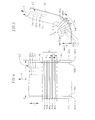
Figure 7 is a schematic view of an arrangement of slits for a flex cable according to an embodiment of the invention. - The present invention relates to flex cables, and more particularly to a temperature tolerant cover layer construction for a flex cable. In one embodiment, a flex cable designed to be bent to a particular curved shape includes one or more slits formed in the inner cover layer, to reduce the amount of material in the cover layer on the inside radius of the curve. By reducing the amount of cover layer material on the inside of the curve, the slits reduce the compressive stress in the cover layer. The slits are formed prior to the process of laminating the flex cable so that upon lamination the flexible filler material below the cover layer fills the slits, providing a compliant, protective layer that bends into the desired curve and protects the active components inside the cable. The slits are sized and spaced according to the dimensions of the cable and the curve. The slits reduce the compressive stress along the inside cover layer and thereby prevent the cover layer from separating from the rest of the cable when the flex cable is subjected to high temperature conditions during manufacturing or during operation. As used herein, "high temperature" means a prolonged exposure (more than a few seconds) at a temperature above 125°C.
- An example of a
flex cable 10 is shown inFigure 1 . Theflex cable 10 is attached to anelectrical component 12, such as an interface feature (such as a connector), a printed circuit board, a sensor in an engine compartment, an electronic device, or many other applications. Theflex cable 10 includes acurved portion 14 for fitting thecomponent 12 andcable 10 into a constrained space and/or for repeated bending during operation. Thecurved portion 14 is shown as a simple bend, but it could be a three-dimensional surface with any curved geometry. Additionally, the cable can bend in both directions, so that the inner side of the curve at one portion becomes the outer side at another bend portion. - Bending the cable into a curved shape introduces stresses into the various layers of the cable. An example of a
prior art cable 100 subject to these stresses is shown inFigure 2 . Thecable 100 includes acore layer 120, aninner layer 122, and anouter layer 124. Thecore layer 120 includes an active element such as aconductor 126. Theinner layer 122 includes acover layer 130 and afiller layer 132, and the outer layer includes acover layer 134 and afiller layer 136. Theselayers conductor element 126 from environmental exposure. - The
cable 100 includes acurved section 114. Thecurved section 114 bends the cable into a curve with an inner radius Ri at theinner cover layer 130 and an outer radius Ro at theouter cover layer 134. Due to the thickness T of thecable 100, the inner radius Ri is shorter than the outer radius Ro. As a result, the length of the curve Li along theinner cover layer 130 is shorter than the length of the curve Lo along theouter cover layer 134. Along thecurved portion 114, theinner cover layer 130 is subjected to compressive stresses, and theouter cover layer 134 is subjected to tensile stresses. - In some prior art cables such as the
cable 100, afiller layer cover layer conductor 126. Thisfiller layer conductor 126 and adheres to thecover conductor 126. However, this type of filler material typically has a low glass transition temperature Tg-filler (for example, approximately 40°C), and its material properties degrade at high temperatures (above 125°C). At these temperatures the material becomes soft and weakens, and the soft layer separates from thecover layer 130. The material of thecover layer - At temperatures above the glass transition temperature of the filler layer, the filler material softens and separates from the cover layer and/or the conductor, as shown in
Figure 2 . Thecover layer 130 is then free to expand outwardly to relieve the compressive stresses in that layer, and a bulge or buckle 116 forms in theinner cover layer 130 at thecurve 114. Thisbuckle 116 creates a void 118 between thecover layer 130 and theadhesive filler 132 and/or between thefiller 132 and theconductor 126. Thefiller 132 may separate, with a portion of it remaining attached to theconductor 126 and a portion remaining attached to thecover layer 130. The separation of thefiller layer 132 may expose theconductor 126, as shown at point A inFigure 2 . Additionally, thebuckle 116 may be exposed at its longitudinal ends, thereby opening the void 118 to the external environment. Thisvoid 118 collects contaminants in its operating environment such as moisture, which can further degrade the layers of the cable and lead to corrosion, short circuits, and mechanical failure of theconductor 126. - As a result, the
cable 100, when formed or bent or otherwise put into a curved or three-dimensional shape, is limited to operating and manufacturing conditions below a certain maximum temperature, to prevent buckles and voids from forming in the cover layer. This temperature maximum limits the number of applications where thecable 100 can be utilized, eliminating some applications with high-temperature operating conditions, such as certain sensors that operate at very high temperatures. - This temperature maximum also limits the manufacturing process for the electrical component that includes the
cable 100. In some situations, a high-temperature soldering process is used to mount sensitive electronic components to a circuit board or other component. When thebent flex cable 100 is temperature-limited, this soldering process must be performed before thecable 100 is bent into its curved shape, while the cable is in an as-laminated minimal internal stress condition. If the cable is bent before soldering, heat from the soldering process can cause thecable 100 to delaminate at thecurve 114, as shown inFigure 2 . If the cable is bent after soldering, thecurved portion 114 is not subjected to this high temperature. However, when the cable is bent after soldering, the bending procedure for forming thecurve 114 can stress the soldered joints and even cause them to fracture and break. Solder joints are often formed in close proximity to bend features, and therefore the bending step can stress the solder joint. Even if the joint does not break, the bending process can create stresses in the solder joint that weaken the structure and cause premature failure. Thus it is desirable to form the bend feature in the cable prior to mounting the sensitive electrical components, so that these electrical components are not subsequently stressed during the bending step. As explained above, such a procedure requires the bent cable to withstand the high temperature soldering process. - To develop an improved temperature tolerant cable, several cables were studied, and delamination such as that shown in
Figure 2 was observed in various flex cables with different types of bend features and bend-forming processes. Accordingly the structure of the cable itself was further studied. Acable 10 with a temperature-tolerant cover layer construction according to an embodiment of the invention is shown inFigure 3 . In this embodiment, thecable 10 includes acore layer 20, aninner layer 22, and anouter layer 24. Thecore layer 20 includes one or more active elements such as conductors. In the embodiment shown, thecore layer 20 includes twoconductors core 29. Thecore 29 is a spacer material that separates the twoconductors cable 10 can include more or fewer conductors, such as one conductor as shown inFigure 2 , or additional conductors separated by additional core layers 29. Theconductors conductors core 29 is a polymer material such as polyimide. An example of a polyimide material is Kapton®, manufactured by Dupont (E. I. du Pont de Nemours and Company). - The
core layer 20 is protected on opposite sides by theinner layer 22 and theouter layer 24. Each of these twoprotective layers cover layer filler layer cover layers cable 10 from being scratched, cut, or punctured. The cover layers 30, 34 may be made from a polymer material such as polyimide (for example, Kapton®). - The two
filler layers cable 10, spacing them apart from the other components of the cable and providing protection against chemicals, corrosion, and other environmental exposure. The filler layers 32, 36 are also used to adhere the cover layers 30, 34 to thecore layer 20, holding thecable 10 together. The filler layer may be made from an acrylic adhesive material. The filler layer is typically a softer material than the scratch-resistant polyimide cover layers 30, 34. - In one embodiment, the
cable 10 is assembled by laminating thelayers layers inner layer 22 is provided as a sheet with thecover layer material 30 already adhered to thefiller layer material 32. A second sheet of the same material is used for theouter layer 24. Thecore layer 20 is also provided as a pre-assembled sheet with the desired number and type of conductors and spacers attached together. For example, thesheet 20 may include copper layers 26, 28 adhesive-lessly attached to thecore layer 29 through a thermal fusion process. - These
sheets layers cover layer respective conductor additional filler layer 38 is provided between theconductor 26 and thefiller layer 32, as described in further detail below. Thelaminated cable 10 is then cooled, and the filler layers 32, 36 reset, holding theouter layers core layer 20 and thus holding the cable together. Thelaminated cable 10 can have a thickness T ranging from 0.01 inches to 0.5 inches. - In the final assembly, the
cable 10 includes acurved section 14 in which thecable 10 curves along an inner radius Ri at thecover layer 30 and an outer radius Ro at thecover layer 34. Thecover layer 30 andfiller layer 32 may be together referred to as the "inner layer" 22 as these layers are inside thecore layer 20 along thecurved section 14, following the inner radius Ri. Thecover layer 34 andfiller layer 36 may together be referred to as the "outer layer" 24, as they are outside of thecore layer 20 along thecurved section 14, following the outer radius Ro. The terms "inner" and "outer" are relative terms used to identify the layers on the opposite sides of thecore layer 20 along thecurved section 14. The term "inner" does not mean that the inner layer is always on the inside, but instead means that with reference to this particular bend feature, the inner layer is on the smaller, inside radius of the curve as compared to the "outer" layer on the opposite side of the core layer. - The
inner cover layer 30 follows the inner radius Ri along thecurved section 14, and theouter cover layer 34 follows the outer radius Ro along thecurved section 14. As mentioned above, due to the thickness T of thecable 10, Ri is less than Ro, and the length Li of thecurve 14 along the inner radius Ri is shorter than the length Lo of thecurve 14 along the outer radius Ro. The shorter length Li along thecover layer 30 creates the potential for compressive stresses within thecover layer 30 along thecurved section 14. - According to an embodiment of the invention, one or
more slits 40a-x are formed in theinner cover layer 30 to relieve such compressive stress. InFigure 3 , thecover layer 30 includes threeslits slits 40a-x reduce the amount of material in thecover layer 30 in order to compensate for the shorter length of thecurve 14 along the inner radius Ri. By removing a small amount of material at the slits, the remainingcover layer material 30 can occupy the slits as necessary to relieve compressive stress when thecover layer 30 is bent. The number, size, and spacing of the slits are designed according to the particular situation, depending on the radius of curvature, the type of material, the expected temperature conditions, and the available manufacturing techniques. In one embodiment, each slit is sized between 0.001 and 0.003 inches in width, and the slits are spaced apart evenly along thecurve 14. The number of slits is determined by the radius of curvature and the amount of material to be removed from theinner layer 30, as described in more detail below. - In one embodiment, the
slits 40a-x are formed by laser-cutting theinner layer 22 before thecable 10 is laminated together.Figure 4 shows an example of an inner layer 22' with fiveslits 40a-e prior to being laminated to a core layer and opposite cover layer to form acable 10. The inner layer 22' is passed through a laser cutting process in which one or more lasers cut theslits 40a-e through the inner layer 22', passing completely through both thecover layer 30 and thefiller layer 32. In one embodiment, the laser burns away the material at theslits 40a-x, removing the material from bothlayers slits 40a-x. In other embodiments, some of the material fromlayer 32 may remain, but at least thecover material 30 is removed along theslits 40a-x. - This inner layer 22' with the
slits 40a-x is then laminated to thecore layer 20 and oppositeouter layer 24 to form thecable 10, as described above. During the lamination process, the layers are heated and pressed together, causing thefiller layer 32 to flow into theslits 40a-x, filling theopenings 42 created by the slits (see theopening 42 inFigure 3 ). In one embodiment, the lamination process includes tooling that prevents thefiller material 32 from flowing up out of the slits, but that allows thismaterial 32 to flow into and fill the slits. Thus, after lamination, thetop surface 31 of theinner cover layer 30 is level across the slits, with thefiller material 32 filling theopenings 42 created by the slits 40. Due to the flexibility of this filler material and its ability to flow during lamination, theslits 40a-x can be formed in thecover layer 30 without leaving depressions or voids in theinner layer 22 of thelaminated cable 10. - These
slits 40a-x create flexible bending points for theinner layer 22 so that it can be bent into thecurve 14, as shown inFigure 3 . Thefiller material 32 is more flexible and pliant than thecover layer 30, so it can bend and move more easily to accommodate thecurve 14. When thecable 10 is bent, thefiller material 32 moves out of the way and allows the strips of cover layer material between adjacent slits to move together across the slit instead of compressing. - The slits may take various geometries after being bent into the
curve 14. Threeexample slits Figure 3 . Thefirst slit 40a has been closed by thecurve 14, as the two portions of thecover layer slit 40a moved together across theslit 40a to accommodate thecurve 14. Thesecond slit 40b includes anopening 42 between the twoportions inner cover layer 30. Theopening 42 is filled by theinner filler layer 32, as described above. As another example, thethird slit 40c includes anoverlap 44 in which an end of thecover layer portion 30d extends over thecover layer portion 30c. These threeslits cover layer 30 andfiller layer 32 can move across the slits to accommodate thecurve 14. In thesevarious slit geometries cover layer 30 when it is curved along the inner radius Ri. - In one embodiment, a cable includes a plurality of slits that are dimensioned according to
slit 40a, without openings 42 (as inslit 40b) or overlaps 44 (as inslit 40c). In such a case, thecover layer portions inner filler layer 32. Theportions portions Figure 2 . In another embodiment, a cable includes a combination ofslits overlap portions 44,openings 42, and/or contactingportions bend feature 14. - In one embodiment, the slits extend across the
cable 10 in a direction that is substantially perpendicular to an axial direction A of thecore layer 20. InFigure 3 , thecore layer 20 has an axial direction A, which is along the axis of theconductor elements Figure 3 , theslits cable 10. The slits extend approximately perpendicular to both the axial direction A and the radial direction Ri / Ro. - A perspective view showing the orientation of the slits is shown in
Figure 5 . In this embodiment, a flex cable 10' according to an embodiment of the invention includes fiveslits 40a-e. The slits extend substantially parallel to each other in a transverse direction T, extending across the width W of the cable 10' transverse to the axial direction A. The axial direction A is the direction along the axis of theconductor elements isolated conductor elements 26a-y can be provided across the width W of the cable 10'. Theslits 40a-x pass across theconductor elements 26a-y extending from oneside edge 10a of the cable to theopposite side edge 10b The cross-sectional view ofFigure 3 is taken along line 3-3 ofFigure 5 (although only threeslits Figure 3 ). - Referring to
Figure 5 , the fiveslits 40a-e are spaced evenly along the length of thecurve 14. That is, the distance d is approximately the same between each slit and between theslits curve - The number, size, and spacing of the slits 40 is determined by the geometry of the curve and the thickness of the particular cable. First, the amount of material to be removed from the
inner cover layer 30 is determined. Referring back toFigure 3 , theinner cover layer 30 is subjected to compressive stress to compress into the shorter length Li, and theouter cover layer 34 is subjected to tensile stress to stretch across the longer length Lo. At some point between these twolayers - In the particular example shown in
Figure 3 , because thecable 10 is substantially symmetric, the neutral axis and minimum-stress layer is approximately at thecore layer 29. Accordingly, to determine the amount of material to be removed by the slits, the length Lc of thecurve 14 along thecore layer 29 is calculated, and the length Li is subtracted from the length Lc. This difference D in length identifies the linear amount of material that should be removed from theinner cover layer 30. - Once this amount D is known, then either the size or the number of slits is selected. In one embodiment, the size w of each slit (see
Figure 4 ) is selected based on the length Li of the curve and/or the capability of the cutting equipment. For example, when laser cutting equipment is used, the laser itself may define a minimum width w for the slits. In one embodiment, the size w of the slits is chosen to be the same as the beam width, so that each slit can be formed with only one pass of the laser across the width W of thesheet 22, rather than multiple passes of the beam to create each slit. In another embodiment, the beam width is chosen based on the speed and operating characteristics of the laser, to provide an efficient and high-speed cutting process. For example, a very wide beam width may move at a slow speed, while a smaller width beam can be moved across the sheet more quickly. In one embodiment, the beam width, and the width w of the slits, is approximately 0.001 inches, and in another embodiment less than 0.001 inches. Based on available laser technology, very fine beams may be used to create slits with widths even as small as 0.0001 inches. The width of the slits can be chosen based on the available beam technology. - As another example, the geometry of the
curve 14 itself may also affect the choice of slit size w. A very wide curve with a relatively large radius may benefit from smaller slits, with a small width w, as the material is not bent very far to form the curve. The size of the slits can be chosen based on these variables. In one embodiment, the slits are between 0.001 and 0.003 inches in size w, and in one embodiment the slits are approximately 0.002 inches in size w. In another embodiment, the width w is approximately the same as the thickness of thecover layer - When the size of each slit is selected, the difference D is divided by the size of each slit w to determine the number x of slits. At this point the length of the curve and the size and number of slits are known. The final geometry of the slits is arranged by evenly spacing the slits along the length Li of the
curve 14. That is, the total amount of material to be removed D is subtracted from the length Li, and then the remaining length is divided by x+1 (the number of slits plus one) to determine the space d between each slit. The laser or other cutting equipment is then programmed to cut the slits of width w at intervals d along the length Li of thecurve portion 14. - Alternatively, the number of slits may be selected first, before the size of each slit is determined. For example, along a very tight curve, there may be room for only a small number of slits. The number x of slits can be pre-selected, and then the difference D is divided by the number x of slits to determine the side w of each slit (see
Figures 4 and 5 ). As before, the difference D is then subtracted from the length Li, and the remaining length is divided by x+1 to determine the space d between each slit. Alternatively, the space d between slits may be selected first and then the size and number of slits can be calculated. - In one embodiment, the number x of slits, size w of slits, and distance d between slits are all considered together to provide an optimal geometry. For example the distance d between slits is considered when choosing the number x of slits, because a large number of slits will require a small distance d between slits. If the distance d is very small then the slits create very thin ribbons of the
cover layer material filler material 32 and move out of place. If the distance d is too small, these ribbons of the cover layer do not provide adequate protection for thecable 10. Thus a minimum size for the distance d is considered, such as 2-3 times the thickness of thecover layer inside cover layer 30. - When the number x of slits, size w of slits, and distance d between slits is determined, laser or other cutting equipment is programmed to create this geometry in the
inner layer 22. Thesheet 22 is passed through the cutting process as described above, to create the slits (see for exampleFigure 4 ). Thesheet 22 is then laminated to thecore layer 20 and theouter layer 24 as described earlier. - Various slit geometries were tested to determine an optimal size, number, and spacing of the
slits 40a-x. In one embodiment, five slits of 0.002 inches each are equally spaced along thecurve 14. In other embodiments, the number of slits can vary from 3 to 7 slits, and the size of each slit can vary from 0.001 inches each to 0.003 inches. - In one embodiment, the slits are created in the flat cable over a distance that is greater than the length Li along the inside of the curve. The extra slits beyond the length of the curve provide tolerance for the formation of the bend feature, so that the bend feature can be misaligned and still be located within the range of the slits. Additionally, the provision of extra slits can enable the same flat cable to be used for various different bend features, which simplifies manufacturing. The same process can be used to create flat cables all having the same slit arrangement, and then these cables can be used to form different bend features.
- In one embodiment, the
cable 10 includes an additionalbase filler layer 38 between theinner layer 22 and the core layer 20 (seeFigure 3 ). Thislayer 38 is provided between thefiller layer 32 and theconductor 26. This layer is added on the inside of thecore layer 20, between the core 20 and theslits 40a-x, to provide additional protection for thecore layer 20. In case any of theslits 40a-x do not completely fill with thefiller layer 32 during lamination, or in case one of the slits leaves anopening 42 that is larger than desired, thebase filler layer 38 provides an extra layer of insulation between the core 20 and the outside environment so that the slits do not expose the cable to environmental degradation. Theextra layer 38 completely covers theconductor 26. Thislayer 38 also provides additional acrylic material that can move and flow into theslits 40a-x during lamination. - Another additional base filler layer such as the
layer 38 may be provided between theouter layer 24 and thecore layer 20 as well. For example, thesame cable 10 can include multiple bend features, such that the layer that is the "inner" layer for one bend feature is the outer layer for a different bend feature. For such a cable, twolayers 38 can be provided on either side of the core. Of course, the slits can then be formed in both cover layers 30, 34. The layer that is the "inner" layer for one bend feature can be the "outer" layer for another bend feature. - As shown in
Figure 4 , in one embodiment theslits 40a-x extend completely across the width W of the layer 22' (and the resulting cable), passing all the way through bothopposite sides layer 22. In one embodiment the layer 22' includesstrips 46a, 46b at each side of thelayer 22 which are removed by cutting along thecut lines strips 46a, 46b are removed and discarded. This step ensures that theslits 40a-x extend completely across the width of the layer 22', so that the slits extend across bothedges - In another embodiment, the slits may be spaced unevenly along the curved section of the cable. Such uneven spacing may be appropriate where the radius of curvature changes along the
curve 14. If the radius increases along the length of the curve (such that the curve becomes wider and less steep), the slits may become more widely spaced along the length of the curve. If the radius decreases along the length of the curve (such that the curve becomes steeper), the slits may become more closely spaced along the length of the curve. In other embodiments there may be additional features in the electrical component that make uneven spacing of the slits desirable. For example a wider space between two slits may be provided where acurve 14 passes near another component, so that thecover layer 30 provides abrasion resistance along the curve near that component. The slits may also be spaced to avoid other features along thecable 10, such as openings or branches for the connection of other components. - The slits described above reduce the compressive stress in the
inner layer 22 and thereby increase the ability of the inner layer to withstand high temperature conditions. Although the slits create openings in thecover layer 30, removing the protective covering material and exposing the softerinner filler layer 32, the number, size, and spacing of the slits is designed for a particular bend feature, so that the resultingcable 10 with the slits provides sufficient protection for the active components within the cable while reducing the compressive stress in theinside cover layer 30. Because the strips of cover layer material between the slits can move together across theopenings 42 created by the slits 40, the compressive stress in this layer is reduced. As a result, thecable 10 can be subjected to higher temperatures without thecover layer 30 delaminating from thefiller layer 32 and creating buckles and voids. - In one embodiment, a flex cable including slits across a bend feature can survive prolonged exposure (more than a few seconds) at temperatures above 125°C, and in another embodiment above 220°C, and in another embodiment above 300°C, and in another embodiment at temperatures up to 350°C. The flex cable can be used in applications such as aerospace, space, marine, and automotive applications, power plants, sensor products, steam turbines, missiles, radar systems, and applications were components operate at temperatures above 125°C.
- The flex cable can also be bent prior to high temperature manufacturing steps, such as a component soldering process, which can elevate the flex cable temperature above 125°C and typically above 220°C. The process for forming the bend feature(s) in the cable prior to high temperature assembly operations can be accomplished with cheaper equipment, without having to work around sensitive or fragile electrical components and soldered joints. As described above, high-temperature manufacturing steps in the prior art were performed with the flex cable in the flat condition, prior to forming bend features in the cable.
- In another embodiment, a cable including slits across a bend feature can be curved into a tighter bend than prior art cables without such slits. In one embodiment, the cable is curved into a radius Ri that is approximately 10-15 times the thickness T of the cable. In one embodiment the radius Ri is 10-20% smaller than in prior applications. The flex cables with tighter bends allow for more complex 3-dimensional shapes to be used in the design and layout of the electrical components in the final assembly.
- Additionally, the use of lasers to form the slits enables slits to be made quickly and accurately. Lamination of the cable layers together after the slits are formed completes the slit features without requiring additional surface treatment or other steps to prepare the cover layer and slits for bending and use.
- A method for constructing a temperature-tolerant flex cable according to an embodiment of the invention is shown in
Figure 6 . The method includes providing an inner layer, an outer layer and acore layer 601, and forming a plurality of slits in theinner layer 602. In one embodiment forming a plurality of slits in the inner layer includes passing a laser beam across the inner layer, as described above, and in one embodiment this includes removing both the cover layer and the filler layer at the slits. The method also includes applying heat and pressure to the layers to adhere them together into acable 603. In one embodiment, this includes moving the filler layer into the slits. In one embodiment, an additional base filler layer is provided between the inner layer and the core layer before the layers are heated and pressed together. The method also includes bending the cable into abend feature 604, with the inner layer on the inside radius of the curve, and exposing the bend feature to a high-temperature condition 605. The high-temperature condition may be a high-temperature soldering step. For example, the method may include mounting the cable to an electrical component, and then soldering a joint on the electrical component at high temperature. - In another embodiment, a flex cable can include slits that are curved or non-parallel. That is, the slits are not necessarily straight, parallel lines. Curved or non-parallel slits may be useful when the cable is curved into a three-dimensional bend feature, such as a sphere. An example of an arrangement of non-parallel slits for a flex cable according to an embodiment of the invention is shown in
Figure 7 . Theslits 240 extend in a radial pattern, with some slits having a longer length and extending further toward the center of the pattern than other slits. This pattern of slits can be formed in a flex cable as described above, and the flex cable can be formed into a three-dimensional bend feature such as bending the cable in a spherical shape. The amount of material removed from the cable (by forming the slits) increases away from the center of the pattern, which corresponds to the "top" of the sphere. The slits also may get wider as they move away from the center. - In the example shown in
Figure 7 , the slits diverge away from the center of the pattern, and they do not intersect. In other embodiments, other patterns of slits can be created, depending on the particular bend feature, including slits that converge, diverge, curve, and/or intersect. - Although the present invention has been described and illustrated in respect to exemplary embodiments, it is to be understood that it is not to be so limited, and changes and modifications may be made therein which are within the full intended scope of this invention as hereinafter claimed. For example, although only one bend feature is shown in the cable in the figures, a single cable can include more than one bend feature, with more than one set of slits. Additionally the cable can have various different layers, including different kinds of conductors or signal elements.
Claims (15)
- A flex cable for bending into a curve, comprising:a core layer comprising a conductor extending in an axial direction;an outer layer covering the core layer along an outside radius of the curve;an inner layer covering the core layer along an inside radius of the curve; andat least one slit formed in the inner layer, the at least one slit extending in a transverse direction that is transverse to the axial direction of the conductor.
- The flex cable of claim 1, wherein the at least one slit comprises a plurality of slits.
- The flex cable of claim 2, wherein the slits are equally spaced along the curve.
- The flex cable of claim 2, wherein the slits have a width, and wherein the slits are equally spaced apart from each other along the curve by a distance that is 2-3 times the width.
- The flex cable of claim 2, wherein the slits are each between 0.001 and 0.003 inches in width.
- The flex cable of claim 1, further comprising a base filler layer between the core layer and the inner layer.
- The flex cable of claim 1, wherein the cable has a thickness and wherein the curve has a radius that is 10-15 times the thickness.
- The flex cable of claim 1, wherein the slit extends across first and second opposite side edges of the inner layer.
- The flex cable of claim 1, wherein the inner layer comprises a cover layer and a filler layer, and wherein the cover layer comprises a first portion and a second portion on opposite sides of the slit, and wherein the first and second portions contact each other.
- The flex cable of claim 1, wherein the cable comprises a plurality of conductors, and wherein the at least one slit extends across each of the conductors.
- The flex cable of claim 1, wherein the inner layer comprises a cover layer and a filler layer, and wherein the slit forms an opening in the cover layer, and wherein the filler layer extends into the opening.
- The flex cable of claim 2, wherein the inner layer comprises a cover layer and a filler layer, and wherein the cover layer comprises a thickness, and wherein each slit has a width that is approximately equal to the thickness.
- A method of constructing a temperature-tolerant flex cable, comprising:providing an inner layer, an outer layer, and a core layer;forming a plurality of slits in the inner layer;applying heat and pressure to the inner layer, the outer layer, and the core layer to adhere them together into a cable;bending the cable into a bend feature, with the inner layer on an inside radius of the bend feature; andexposing the bend feature to a high-temperature condition.
- The method of claim 13, wherein the inner layer comprises a cover layer and a filler layer, and wherein forming the plurality of slits comprises removing both the cover layer and the filler layer at the slit.
- The method of claim 14, wherein applying heat and pressure comprises moving the filler layer into the plurality of slits.
Applications Claiming Priority (1)
| Application Number | Priority Date | Filing Date | Title |
|---|---|---|---|
| US12/781,642 US8324505B2 (en) | 2010-05-17 | 2010-05-17 | Temperature tolerant cover layer construction |
Publications (2)
| Publication Number | Publication Date |
|---|---|
| EP2388786A1 true EP2388786A1 (en) | 2011-11-23 |
| EP2388786B1 EP2388786B1 (en) | 2013-06-26 |
Family
ID=44262542
Family Applications (1)
| Application Number | Title | Priority Date | Filing Date |
|---|---|---|---|
| EP11158484.3A Active EP2388786B1 (en) | 2010-05-17 | 2011-03-16 | Temperature tolerant cover layer construction |
Country Status (3)
| Country | Link |
|---|---|
| US (1) | US8324505B2 (en) |
| EP (1) | EP2388786B1 (en) |
| IL (1) | IL211472A (en) |
Families Citing this family (1)
| Publication number | Priority date | Publication date | Assignee | Title |
|---|---|---|---|---|
| KR101554304B1 (en) * | 2015-04-20 | 2015-09-18 | 한솔테크닉스(주) | Curved type rigid board and a Three-dimension antenna manufacturing method of using the same |
Citations (2)
| Publication number | Priority date | Publication date | Assignee | Title |
|---|---|---|---|---|
| JPH0343912A (en) * | 1989-07-12 | 1991-02-25 | Fujikura Ltd | Insulated cable |
| US6224395B1 (en) * | 1997-05-28 | 2001-05-01 | International Business Machines Corporation | Flex cables with increased three-dimensional conformity and design flexibility |
Family Cites Families (1)
| Publication number | Priority date | Publication date | Assignee | Title |
|---|---|---|---|---|
| EP0650166B1 (en) * | 1993-04-16 | 2000-01-05 | Kabushiki Kaisha Toshiba | Electronic equipment and disc reproducing device |
-
2010
- 2010-05-17 US US12/781,642 patent/US8324505B2/en active Active
-
2011
- 2011-02-28 IL IL211472A patent/IL211472A/en active IP Right Grant
- 2011-03-16 EP EP11158484.3A patent/EP2388786B1/en active Active
Patent Citations (2)
| Publication number | Priority date | Publication date | Assignee | Title |
|---|---|---|---|---|
| JPH0343912A (en) * | 1989-07-12 | 1991-02-25 | Fujikura Ltd | Insulated cable |
| US6224395B1 (en) * | 1997-05-28 | 2001-05-01 | International Business Machines Corporation | Flex cables with increased three-dimensional conformity and design flexibility |
Also Published As
| Publication number | Publication date |
|---|---|
| US20110278046A1 (en) | 2011-11-17 |
| IL211472A0 (en) | 2011-06-30 |
| EP2388786B1 (en) | 2013-06-26 |
| IL211472A (en) | 2014-03-31 |
| US8324505B2 (en) | 2012-12-04 |
Similar Documents
| Publication | Publication Date | Title |
|---|---|---|
| TWI402863B (en) | Coaxial beam | |
| US6657126B2 (en) | Wire branch processing for shielded wire | |
| RU2494508C2 (en) | Unit of connector and electric paths | |
| US9474149B2 (en) | Angle-adjustable and/or angled printed circuit board structure having at least two printed circuit board sections and method for producing the same | |
| JP6098217B2 (en) | Circuit board and manufacturing method thereof | |
| EP2147482B1 (en) | Connector for an electrical circuit embedded in a composite structure and method for manufacturing | |
| US7772496B2 (en) | Flat cable | |
| EP1915037A1 (en) | Bending-type rigid printed wiring board and process for producing the same | |
| US11791577B2 (en) | Forming connections to flexible interconnect circuits | |
| EP2388786B1 (en) | Temperature tolerant cover layer construction | |
| US10410759B2 (en) | Conductive device intended to be mounted on the surface of parts made of composite materials | |
| WO2022202667A1 (en) | Wiring member | |
| JP5812454B2 (en) | Multi-core shielded flat cable and method of manufacturing multi-core shielded flat cable | |
| KR102423487B1 (en) | Method For Manufacturing Flexible Flat Cable And Flexible Flat Cable Manufactured Thereby | |
| JP4918917B2 (en) | Flat cable manufacturing method | |
| JP2010218832A (en) | Flat cable and method of manufacturing the same | |
| KR101749803B1 (en) | Wiring member | |
| JP5868240B2 (en) | Flat cable and circuit board with flat cable | |
| JP2014154280A (en) | Flat wiring material and method for producing the same | |
| KR101052160B1 (en) | Flat cable with multiple wiring layers | |
| JP2005093267A (en) | Branch structure of flat harness and its manufacturing method |
Legal Events
| Date | Code | Title | Description |
|---|---|---|---|
| 17P | Request for examination filed |
Effective date: 20110412 |
|
| AK | Designated contracting states |
Kind code of ref document: A1 Designated state(s): AL AT BE BG CH CY CZ DE DK EE ES FI FR GB GR HR HU IE IS IT LI LT LU LV MC MK MT NL NO PL PT RO RS SE SI SK SM TR |
|
| AX | Request for extension of the european patent |
Extension state: BA ME |
|
| PUAI | Public reference made under article 153(3) epc to a published international application that has entered the european phase |
Free format text: ORIGINAL CODE: 0009012 |
|
| RIC1 | Information provided on ipc code assigned before grant |
Ipc: H01B 7/04 20060101AFI20120815BHEP Ipc: H01R 12/77 20110101ALI20120815BHEP Ipc: H01R 12/59 20110101ALI20120815BHEP |
|
| GRAP | Despatch of communication of intention to grant a patent |
Free format text: ORIGINAL CODE: EPIDOSNIGR1 |
|
| GRAC | Information related to communication of intention to grant a patent modified |
Free format text: ORIGINAL CODE: EPIDOSCIGR1 |
|
| GRAS | Grant fee paid |
Free format text: ORIGINAL CODE: EPIDOSNIGR3 |
|
| GRAA | (expected) grant |
Free format text: ORIGINAL CODE: 0009210 |
|
| AK | Designated contracting states |
Kind code of ref document: B1 Designated state(s): AL AT BE BG CH CY CZ DE DK EE ES FI FR GB GR HR HU IE IS IT LI LT LU LV MC MK MT NL NO PL PT RO RS SE SI SK SM TR |
|
| REG | Reference to a national code |
Ref country code: GB Ref legal event code: FG4D |
|
| REG | Reference to a national code |
Ref country code: CH Ref legal event code: EP |
|
| REG | Reference to a national code |
Ref country code: AT Ref legal event code: REF Ref document number: 619016 Country of ref document: AT Kind code of ref document: T Effective date: 20130715 |
|
| REG | Reference to a national code |
Ref country code: IE Ref legal event code: FG4D |
|
| REG | Reference to a national code |
Ref country code: DE Ref legal event code: R096 Ref document number: 602011002107 Country of ref document: DE Effective date: 20130829 |
|
| PG25 | Lapsed in a contracting state [announced via postgrant information from national office to epo] |
Ref country code: LT Free format text: LAPSE BECAUSE OF FAILURE TO SUBMIT A TRANSLATION OF THE DESCRIPTION OR TO PAY THE FEE WITHIN THE PRESCRIBED TIME-LIMIT Effective date: 20130626 Ref country code: FI Free format text: LAPSE BECAUSE OF FAILURE TO SUBMIT A TRANSLATION OF THE DESCRIPTION OR TO PAY THE FEE WITHIN THE PRESCRIBED TIME-LIMIT Effective date: 20130626 Ref country code: SI Free format text: LAPSE BECAUSE OF FAILURE TO SUBMIT A TRANSLATION OF THE DESCRIPTION OR TO PAY THE FEE WITHIN THE PRESCRIBED TIME-LIMIT Effective date: 20130626 Ref country code: GR Free format text: LAPSE BECAUSE OF FAILURE TO SUBMIT A TRANSLATION OF THE DESCRIPTION OR TO PAY THE FEE WITHIN THE PRESCRIBED TIME-LIMIT Effective date: 20130927 Ref country code: NO Free format text: LAPSE BECAUSE OF FAILURE TO SUBMIT A TRANSLATION OF THE DESCRIPTION OR TO PAY THE FEE WITHIN THE PRESCRIBED TIME-LIMIT Effective date: 20130926 Ref country code: SE Free format text: LAPSE BECAUSE OF FAILURE TO SUBMIT A TRANSLATION OF THE DESCRIPTION OR TO PAY THE FEE WITHIN THE PRESCRIBED TIME-LIMIT Effective date: 20130626 |
|
| REG | Reference to a national code |
Ref country code: AT Ref legal event code: MK05 Ref document number: 619016 Country of ref document: AT Kind code of ref document: T Effective date: 20130626 |
|
| REG | Reference to a national code |
Ref country code: LT Ref legal event code: MG4D |
|
| PG25 | Lapsed in a contracting state [announced via postgrant information from national office to epo] |
Ref country code: HR Free format text: LAPSE BECAUSE OF FAILURE TO SUBMIT A TRANSLATION OF THE DESCRIPTION OR TO PAY THE FEE WITHIN THE PRESCRIBED TIME-LIMIT Effective date: 20130626 Ref country code: BG Free format text: LAPSE BECAUSE OF FAILURE TO SUBMIT A TRANSLATION OF THE DESCRIPTION OR TO PAY THE FEE WITHIN THE PRESCRIBED TIME-LIMIT Effective date: 20130926 Ref country code: RS Free format text: LAPSE BECAUSE OF FAILURE TO SUBMIT A TRANSLATION OF THE DESCRIPTION OR TO PAY THE FEE WITHIN THE PRESCRIBED TIME-LIMIT Effective date: 20130626 |
|
| REG | Reference to a national code |
Ref country code: NL Ref legal event code: VDEP Effective date: 20130626 |
|
| PG25 | Lapsed in a contracting state [announced via postgrant information from national office to epo] |
Ref country code: LV Free format text: LAPSE BECAUSE OF FAILURE TO SUBMIT A TRANSLATION OF THE DESCRIPTION OR TO PAY THE FEE WITHIN THE PRESCRIBED TIME-LIMIT Effective date: 20130626 |
|
| PG25 | Lapsed in a contracting state [announced via postgrant information from national office to epo] |
Ref country code: AT Free format text: LAPSE BECAUSE OF FAILURE TO SUBMIT A TRANSLATION OF THE DESCRIPTION OR TO PAY THE FEE WITHIN THE PRESCRIBED TIME-LIMIT Effective date: 20130626 Ref country code: CY Free format text: LAPSE BECAUSE OF FAILURE TO SUBMIT A TRANSLATION OF THE DESCRIPTION OR TO PAY THE FEE WITHIN THE PRESCRIBED TIME-LIMIT Effective date: 20130731 Ref country code: IS Free format text: LAPSE BECAUSE OF FAILURE TO SUBMIT A TRANSLATION OF THE DESCRIPTION OR TO PAY THE FEE WITHIN THE PRESCRIBED TIME-LIMIT Effective date: 20131026 Ref country code: CZ Free format text: LAPSE BECAUSE OF FAILURE TO SUBMIT A TRANSLATION OF THE DESCRIPTION OR TO PAY THE FEE WITHIN THE PRESCRIBED TIME-LIMIT Effective date: 20130626 Ref country code: BE Free format text: LAPSE BECAUSE OF FAILURE TO SUBMIT A TRANSLATION OF THE DESCRIPTION OR TO PAY THE FEE WITHIN THE PRESCRIBED TIME-LIMIT Effective date: 20130626 Ref country code: SK Free format text: LAPSE BECAUSE OF FAILURE TO SUBMIT A TRANSLATION OF THE DESCRIPTION OR TO PAY THE FEE WITHIN THE PRESCRIBED TIME-LIMIT Effective date: 20130626 Ref country code: PT Free format text: LAPSE BECAUSE OF FAILURE TO SUBMIT A TRANSLATION OF THE DESCRIPTION OR TO PAY THE FEE WITHIN THE PRESCRIBED TIME-LIMIT Effective date: 20131028 Ref country code: EE Free format text: LAPSE BECAUSE OF FAILURE TO SUBMIT A TRANSLATION OF THE DESCRIPTION OR TO PAY THE FEE WITHIN THE PRESCRIBED TIME-LIMIT Effective date: 20130626 |
|
| PG25 | Lapsed in a contracting state [announced via postgrant information from national office to epo] |
Ref country code: NL Free format text: LAPSE BECAUSE OF FAILURE TO SUBMIT A TRANSLATION OF THE DESCRIPTION OR TO PAY THE FEE WITHIN THE PRESCRIBED TIME-LIMIT Effective date: 20130626 Ref country code: PL Free format text: LAPSE BECAUSE OF FAILURE TO SUBMIT A TRANSLATION OF THE DESCRIPTION OR TO PAY THE FEE WITHIN THE PRESCRIBED TIME-LIMIT Effective date: 20130626 Ref country code: RO Free format text: LAPSE BECAUSE OF FAILURE TO SUBMIT A TRANSLATION OF THE DESCRIPTION OR TO PAY THE FEE WITHIN THE PRESCRIBED TIME-LIMIT Effective date: 20130626 Ref country code: ES Free format text: LAPSE BECAUSE OF FAILURE TO SUBMIT A TRANSLATION OF THE DESCRIPTION OR TO PAY THE FEE WITHIN THE PRESCRIBED TIME-LIMIT Effective date: 20131007 |
|
| PG25 | Lapsed in a contracting state [announced via postgrant information from national office to epo] |
Ref country code: CY Free format text: LAPSE BECAUSE OF FAILURE TO SUBMIT A TRANSLATION OF THE DESCRIPTION OR TO PAY THE FEE WITHIN THE PRESCRIBED TIME-LIMIT Effective date: 20130626 |
|
| PG25 | Lapsed in a contracting state [announced via postgrant information from national office to epo] |
Ref country code: DK Free format text: LAPSE BECAUSE OF FAILURE TO SUBMIT A TRANSLATION OF THE DESCRIPTION OR TO PAY THE FEE WITHIN THE PRESCRIBED TIME-LIMIT Effective date: 20130626 |
|
| PLBE | No opposition filed within time limit |
Free format text: ORIGINAL CODE: 0009261 |
|
| STAA | Information on the status of an ep patent application or granted ep patent |
Free format text: STATUS: NO OPPOSITION FILED WITHIN TIME LIMIT |
|
| PG25 | Lapsed in a contracting state [announced via postgrant information from national office to epo] |
Ref country code: IT Free format text: LAPSE BECAUSE OF FAILURE TO SUBMIT A TRANSLATION OF THE DESCRIPTION OR TO PAY THE FEE WITHIN THE PRESCRIBED TIME-LIMIT Effective date: 20130626 |
|
| 26N | No opposition filed |
Effective date: 20140327 |
|
| REG | Reference to a national code |
Ref country code: DE Ref legal event code: R097 Ref document number: 602011002107 Country of ref document: DE Effective date: 20140327 |
|
| PG25 | Lapsed in a contracting state [announced via postgrant information from national office to epo] |
Ref country code: LU Free format text: LAPSE BECAUSE OF FAILURE TO SUBMIT A TRANSLATION OF THE DESCRIPTION OR TO PAY THE FEE WITHIN THE PRESCRIBED TIME-LIMIT Effective date: 20140316 |
|
| REG | Reference to a national code |
Ref country code: CH Ref legal event code: PL |
|
| REG | Reference to a national code |
Ref country code: IE Ref legal event code: MM4A |
|
| PG25 | Lapsed in a contracting state [announced via postgrant information from national office to epo] |
Ref country code: IE Free format text: LAPSE BECAUSE OF NON-PAYMENT OF DUE FEES Effective date: 20140316 Ref country code: LI Free format text: LAPSE BECAUSE OF NON-PAYMENT OF DUE FEES Effective date: 20140331 Ref country code: CH Free format text: LAPSE BECAUSE OF NON-PAYMENT OF DUE FEES Effective date: 20140331 |
|
| REG | Reference to a national code |
Ref country code: FR Ref legal event code: PLFP Year of fee payment: 5 |
|
| REG | Reference to a national code |
Ref country code: FR Ref legal event code: PLFP Year of fee payment: 6 |
|
| PG25 | Lapsed in a contracting state [announced via postgrant information from national office to epo] |
Ref country code: MT Free format text: LAPSE BECAUSE OF FAILURE TO SUBMIT A TRANSLATION OF THE DESCRIPTION OR TO PAY THE FEE WITHIN THE PRESCRIBED TIME-LIMIT Effective date: 20130626 |
|
| PG25 | Lapsed in a contracting state [announced via postgrant information from national office to epo] |
Ref country code: SM Free format text: LAPSE BECAUSE OF FAILURE TO SUBMIT A TRANSLATION OF THE DESCRIPTION OR TO PAY THE FEE WITHIN THE PRESCRIBED TIME-LIMIT Effective date: 20130626 |
|
| PG25 | Lapsed in a contracting state [announced via postgrant information from national office to epo] |
Ref country code: MC Free format text: LAPSE BECAUSE OF FAILURE TO SUBMIT A TRANSLATION OF THE DESCRIPTION OR TO PAY THE FEE WITHIN THE PRESCRIBED TIME-LIMIT Effective date: 20130626 |
|
| PG25 | Lapsed in a contracting state [announced via postgrant information from national office to epo] |
Ref country code: TR Free format text: LAPSE BECAUSE OF FAILURE TO SUBMIT A TRANSLATION OF THE DESCRIPTION OR TO PAY THE FEE WITHIN THE PRESCRIBED TIME-LIMIT Effective date: 20130626 Ref country code: HU Free format text: LAPSE BECAUSE OF FAILURE TO SUBMIT A TRANSLATION OF THE DESCRIPTION OR TO PAY THE FEE WITHIN THE PRESCRIBED TIME-LIMIT; INVALID AB INITIO Effective date: 20110316 |
|
| REG | Reference to a national code |
Ref country code: FR Ref legal event code: PLFP Year of fee payment: 7 |
|
| REG | Reference to a national code |
Ref country code: FR Ref legal event code: PLFP Year of fee payment: 8 |
|
| PG25 | Lapsed in a contracting state [announced via postgrant information from national office to epo] |
Ref country code: MK Free format text: LAPSE BECAUSE OF FAILURE TO SUBMIT A TRANSLATION OF THE DESCRIPTION OR TO PAY THE FEE WITHIN THE PRESCRIBED TIME-LIMIT Effective date: 20130626 |
|
| PG25 | Lapsed in a contracting state [announced via postgrant information from national office to epo] |
Ref country code: AL Free format text: LAPSE BECAUSE OF FAILURE TO SUBMIT A TRANSLATION OF THE DESCRIPTION OR TO PAY THE FEE WITHIN THE PRESCRIBED TIME-LIMIT Effective date: 20130626 |
|
| PGFP | Annual fee paid to national office [announced via postgrant information from national office to epo] |
Ref country code: FR Payment date: 20230222 Year of fee payment: 13 |
|
| PGFP | Annual fee paid to national office [announced via postgrant information from national office to epo] |
Ref country code: GB Payment date: 20230222 Year of fee payment: 13 Ref country code: DE Payment date: 20230221 Year of fee payment: 13 |
|
| P01 | Opt-out of the competence of the unified patent court (upc) registered |
Effective date: 20230530 |