EP2387295A1 - IC-Packung mit integrierter Impedanzanpassung und harmonischer Unterdrückung - Google Patents
IC-Packung mit integrierter Impedanzanpassung und harmonischer Unterdrückung Download PDFInfo
- Publication number
- EP2387295A1 EP2387295A1 EP20100162427 EP10162427A EP2387295A1 EP 2387295 A1 EP2387295 A1 EP 2387295A1 EP 20100162427 EP20100162427 EP 20100162427 EP 10162427 A EP10162427 A EP 10162427A EP 2387295 A1 EP2387295 A1 EP 2387295A1
- Authority
- EP
- European Patent Office
- Prior art keywords
- package
- layer
- circuit
- stubs
- pair
- Prior art date
- Legal status (The legal status is an assumption and is not a legal conclusion. Google has not performed a legal analysis and makes no representation as to the accuracy of the status listed.)
- Withdrawn
Links
Images


Classifications
-
- H—ELECTRICITY
- H01—ELECTRIC ELEMENTS
- H01L—SEMICONDUCTOR DEVICES NOT COVERED BY CLASS H10
- H01L23/00—Details of semiconductor or other solid state devices
- H01L23/58—Structural electrical arrangements for semiconductor devices not otherwise provided for, e.g. in combination with batteries
- H01L23/64—Impedance arrangements
- H01L23/66—High-frequency adaptations
-
- H—ELECTRICITY
- H01—ELECTRIC ELEMENTS
- H01P—WAVEGUIDES; RESONATORS, LINES, OR OTHER DEVICES OF THE WAVEGUIDE TYPE
- H01P5/00—Coupling devices of the waveguide type
- H01P5/08—Coupling devices of the waveguide type for linking dissimilar lines or devices
- H01P5/10—Coupling devices of the waveguide type for linking dissimilar lines or devices for coupling balanced with unbalanced lines or devices
-
- H—ELECTRICITY
- H03—ELECTRONIC CIRCUITRY
- H03F—AMPLIFIERS
- H03F1/00—Details of amplifiers with only discharge tubes, only semiconductor devices or only unspecified devices as amplifying elements
- H03F1/56—Modifications of input or output impedances, not otherwise provided for
- H03F1/565—Modifications of input or output impedances, not otherwise provided for using inductive elements
-
- H—ELECTRICITY
- H03—ELECTRONIC CIRCUITRY
- H03F—AMPLIFIERS
- H03F3/00—Amplifiers with only discharge tubes or only semiconductor devices as amplifying elements
- H03F3/45—Differential amplifiers
- H03F3/45071—Differential amplifiers with semiconductor devices only
- H03F3/45076—Differential amplifiers with semiconductor devices only characterised by the way of implementation of the active amplifying circuit in the differential amplifier
- H03F3/45475—Differential amplifiers with semiconductor devices only characterised by the way of implementation of the active amplifying circuit in the differential amplifier using IC blocks as the active amplifying circuit
-
- H—ELECTRICITY
- H05—ELECTRIC TECHNIQUES NOT OTHERWISE PROVIDED FOR
- H05K—PRINTED CIRCUITS; CASINGS OR CONSTRUCTIONAL DETAILS OF ELECTRIC APPARATUS; MANUFACTURE OF ASSEMBLAGES OF ELECTRICAL COMPONENTS
- H05K1/00—Printed circuits
- H05K1/02—Details
- H05K1/0213—Electrical arrangements not otherwise provided for
- H05K1/0237—High frequency adaptations
- H05K1/025—Impedance arrangements, e.g. impedance matching, reduction of parasitic impedance
- H05K1/0251—Impedance arrangements, e.g. impedance matching, reduction of parasitic impedance related to vias or transitions between vias and transmission lines
-
- H—ELECTRICITY
- H01—ELECTRIC ELEMENTS
- H01L—SEMICONDUCTOR DEVICES NOT COVERED BY CLASS H10
- H01L2223/00—Details relating to semiconductor or other solid state devices covered by the group H01L23/00
- H01L2223/58—Structural electrical arrangements for semiconductor devices not otherwise provided for
- H01L2223/64—Impedance arrangements
- H01L2223/66—High-frequency adaptations
- H01L2223/6605—High-frequency electrical connections
- H01L2223/6627—Waveguides, e.g. microstrip line, strip line, coplanar line
-
- H—ELECTRICITY
- H01—ELECTRIC ELEMENTS
- H01L—SEMICONDUCTOR DEVICES NOT COVERED BY CLASS H10
- H01L2223/00—Details relating to semiconductor or other solid state devices covered by the group H01L23/00
- H01L2223/58—Structural electrical arrangements for semiconductor devices not otherwise provided for
- H01L2223/64—Impedance arrangements
- H01L2223/66—High-frequency adaptations
- H01L2223/6644—Packaging aspects of high-frequency amplifiers
- H01L2223/6655—Matching arrangements, e.g. arrangement of inductive and capacitive components
-
- H—ELECTRICITY
- H01—ELECTRIC ELEMENTS
- H01L—SEMICONDUCTOR DEVICES NOT COVERED BY CLASS H10
- H01L2224/00—Indexing scheme for arrangements for connecting or disconnecting semiconductor or solid-state bodies and methods related thereto as covered by H01L24/00
- H01L2224/01—Means for bonding being attached to, or being formed on, the surface to be connected, e.g. chip-to-package, die-attach, "first-level" interconnects; Manufacturing methods related thereto
- H01L2224/02—Bonding areas; Manufacturing methods related thereto
- H01L2224/04—Structure, shape, material or disposition of the bonding areas prior to the connecting process
- H01L2224/05—Structure, shape, material or disposition of the bonding areas prior to the connecting process of an individual bonding area
- H01L2224/0554—External layer
- H01L2224/0555—Shape
- H01L2224/05552—Shape in top view
- H01L2224/05554—Shape in top view being square
-
- H—ELECTRICITY
- H01—ELECTRIC ELEMENTS
- H01L—SEMICONDUCTOR DEVICES NOT COVERED BY CLASS H10
- H01L2224/00—Indexing scheme for arrangements for connecting or disconnecting semiconductor or solid-state bodies and methods related thereto as covered by H01L24/00
- H01L2224/01—Means for bonding being attached to, or being formed on, the surface to be connected, e.g. chip-to-package, die-attach, "first-level" interconnects; Manufacturing methods related thereto
- H01L2224/42—Wire connectors; Manufacturing methods related thereto
- H01L2224/44—Structure, shape, material or disposition of the wire connectors prior to the connecting process
- H01L2224/45—Structure, shape, material or disposition of the wire connectors prior to the connecting process of an individual wire connector
- H01L2224/45001—Core members of the connector
- H01L2224/4501—Shape
- H01L2224/45012—Cross-sectional shape
- H01L2224/45015—Cross-sectional shape being circular
-
- H—ELECTRICITY
- H01—ELECTRIC ELEMENTS
- H01L—SEMICONDUCTOR DEVICES NOT COVERED BY CLASS H10
- H01L2224/00—Indexing scheme for arrangements for connecting or disconnecting semiconductor or solid-state bodies and methods related thereto as covered by H01L24/00
- H01L2224/01—Means for bonding being attached to, or being formed on, the surface to be connected, e.g. chip-to-package, die-attach, "first-level" interconnects; Manufacturing methods related thereto
- H01L2224/42—Wire connectors; Manufacturing methods related thereto
- H01L2224/44—Structure, shape, material or disposition of the wire connectors prior to the connecting process
- H01L2224/45—Structure, shape, material or disposition of the wire connectors prior to the connecting process of an individual wire connector
- H01L2224/45001—Core members of the connector
- H01L2224/45099—Material
- H01L2224/451—Material with a principal constituent of the material being a metal or a metalloid, e.g. boron (B), silicon (Si), germanium (Ge), arsenic (As), antimony (Sb), tellurium (Te) and polonium (Po), and alloys thereof
- H01L2224/45117—Material with a principal constituent of the material being a metal or a metalloid, e.g. boron (B), silicon (Si), germanium (Ge), arsenic (As), antimony (Sb), tellurium (Te) and polonium (Po), and alloys thereof the principal constituent melting at a temperature of greater than or equal to 400°C and less than 950°C
- H01L2224/45124—Aluminium (Al) as principal constituent
-
- H—ELECTRICITY
- H01—ELECTRIC ELEMENTS
- H01L—SEMICONDUCTOR DEVICES NOT COVERED BY CLASS H10
- H01L2224/00—Indexing scheme for arrangements for connecting or disconnecting semiconductor or solid-state bodies and methods related thereto as covered by H01L24/00
- H01L2224/01—Means for bonding being attached to, or being formed on, the surface to be connected, e.g. chip-to-package, die-attach, "first-level" interconnects; Manufacturing methods related thereto
- H01L2224/42—Wire connectors; Manufacturing methods related thereto
- H01L2224/44—Structure, shape, material or disposition of the wire connectors prior to the connecting process
- H01L2224/45—Structure, shape, material or disposition of the wire connectors prior to the connecting process of an individual wire connector
- H01L2224/45001—Core members of the connector
- H01L2224/45099—Material
- H01L2224/451—Material with a principal constituent of the material being a metal or a metalloid, e.g. boron (B), silicon (Si), germanium (Ge), arsenic (As), antimony (Sb), tellurium (Te) and polonium (Po), and alloys thereof
- H01L2224/45138—Material with a principal constituent of the material being a metal or a metalloid, e.g. boron (B), silicon (Si), germanium (Ge), arsenic (As), antimony (Sb), tellurium (Te) and polonium (Po), and alloys thereof the principal constituent melting at a temperature of greater than or equal to 950°C and less than 1550°C
- H01L2224/45144—Gold (Au) as principal constituent
-
- H—ELECTRICITY
- H01—ELECTRIC ELEMENTS
- H01L—SEMICONDUCTOR DEVICES NOT COVERED BY CLASS H10
- H01L2224/00—Indexing scheme for arrangements for connecting or disconnecting semiconductor or solid-state bodies and methods related thereto as covered by H01L24/00
- H01L2224/01—Means for bonding being attached to, or being formed on, the surface to be connected, e.g. chip-to-package, die-attach, "first-level" interconnects; Manufacturing methods related thereto
- H01L2224/42—Wire connectors; Manufacturing methods related thereto
- H01L2224/44—Structure, shape, material or disposition of the wire connectors prior to the connecting process
- H01L2224/45—Structure, shape, material or disposition of the wire connectors prior to the connecting process of an individual wire connector
- H01L2224/45001—Core members of the connector
- H01L2224/45099—Material
- H01L2224/451—Material with a principal constituent of the material being a metal or a metalloid, e.g. boron (B), silicon (Si), germanium (Ge), arsenic (As), antimony (Sb), tellurium (Te) and polonium (Po), and alloys thereof
- H01L2224/45138—Material with a principal constituent of the material being a metal or a metalloid, e.g. boron (B), silicon (Si), germanium (Ge), arsenic (As), antimony (Sb), tellurium (Te) and polonium (Po), and alloys thereof the principal constituent melting at a temperature of greater than or equal to 950°C and less than 1550°C
- H01L2224/45147—Copper (Cu) as principal constituent
-
- H—ELECTRICITY
- H01—ELECTRIC ELEMENTS
- H01L—SEMICONDUCTOR DEVICES NOT COVERED BY CLASS H10
- H01L2224/00—Indexing scheme for arrangements for connecting or disconnecting semiconductor or solid-state bodies and methods related thereto as covered by H01L24/00
- H01L2224/01—Means for bonding being attached to, or being formed on, the surface to be connected, e.g. chip-to-package, die-attach, "first-level" interconnects; Manufacturing methods related thereto
- H01L2224/42—Wire connectors; Manufacturing methods related thereto
- H01L2224/47—Structure, shape, material or disposition of the wire connectors after the connecting process
- H01L2224/48—Structure, shape, material or disposition of the wire connectors after the connecting process of an individual wire connector
- H01L2224/4805—Shape
- H01L2224/4809—Loop shape
- H01L2224/48091—Arched
-
- H—ELECTRICITY
- H01—ELECTRIC ELEMENTS
- H01L—SEMICONDUCTOR DEVICES NOT COVERED BY CLASS H10
- H01L2224/00—Indexing scheme for arrangements for connecting or disconnecting semiconductor or solid-state bodies and methods related thereto as covered by H01L24/00
- H01L2224/01—Means for bonding being attached to, or being formed on, the surface to be connected, e.g. chip-to-package, die-attach, "first-level" interconnects; Manufacturing methods related thereto
- H01L2224/42—Wire connectors; Manufacturing methods related thereto
- H01L2224/47—Structure, shape, material or disposition of the wire connectors after the connecting process
- H01L2224/48—Structure, shape, material or disposition of the wire connectors after the connecting process of an individual wire connector
- H01L2224/481—Disposition
- H01L2224/48151—Connecting between a semiconductor or solid-state body and an item not being a semiconductor or solid-state body, e.g. chip-to-substrate, chip-to-passive
- H01L2224/48221—Connecting between a semiconductor or solid-state body and an item not being a semiconductor or solid-state body, e.g. chip-to-substrate, chip-to-passive the body and the item being stacked
- H01L2224/48225—Connecting between a semiconductor or solid-state body and an item not being a semiconductor or solid-state body, e.g. chip-to-substrate, chip-to-passive the body and the item being stacked the item being non-metallic, e.g. insulating substrate with or without metallisation
- H01L2224/48227—Connecting between a semiconductor or solid-state body and an item not being a semiconductor or solid-state body, e.g. chip-to-substrate, chip-to-passive the body and the item being stacked the item being non-metallic, e.g. insulating substrate with or without metallisation connecting the wire to a bond pad of the item
-
- H—ELECTRICITY
- H01—ELECTRIC ELEMENTS
- H01L—SEMICONDUCTOR DEVICES NOT COVERED BY CLASS H10
- H01L2224/00—Indexing scheme for arrangements for connecting or disconnecting semiconductor or solid-state bodies and methods related thereto as covered by H01L24/00
- H01L2224/01—Means for bonding being attached to, or being formed on, the surface to be connected, e.g. chip-to-package, die-attach, "first-level" interconnects; Manufacturing methods related thereto
- H01L2224/42—Wire connectors; Manufacturing methods related thereto
- H01L2224/47—Structure, shape, material or disposition of the wire connectors after the connecting process
- H01L2224/49—Structure, shape, material or disposition of the wire connectors after the connecting process of a plurality of wire connectors
- H01L2224/491—Disposition
- H01L2224/4912—Layout
- H01L2224/49171—Fan-out arrangements
-
- H—ELECTRICITY
- H01—ELECTRIC ELEMENTS
- H01L—SEMICONDUCTOR DEVICES NOT COVERED BY CLASS H10
- H01L24/00—Arrangements for connecting or disconnecting semiconductor or solid-state bodies; Methods or apparatus related thereto
- H01L24/01—Means for bonding being attached to, or being formed on, the surface to be connected, e.g. chip-to-package, die-attach, "first-level" interconnects; Manufacturing methods related thereto
- H01L24/42—Wire connectors; Manufacturing methods related thereto
- H01L24/44—Structure, shape, material or disposition of the wire connectors prior to the connecting process
- H01L24/45—Structure, shape, material or disposition of the wire connectors prior to the connecting process of an individual wire connector
-
- H—ELECTRICITY
- H01—ELECTRIC ELEMENTS
- H01L—SEMICONDUCTOR DEVICES NOT COVERED BY CLASS H10
- H01L24/00—Arrangements for connecting or disconnecting semiconductor or solid-state bodies; Methods or apparatus related thereto
- H01L24/01—Means for bonding being attached to, or being formed on, the surface to be connected, e.g. chip-to-package, die-attach, "first-level" interconnects; Manufacturing methods related thereto
- H01L24/42—Wire connectors; Manufacturing methods related thereto
- H01L24/47—Structure, shape, material or disposition of the wire connectors after the connecting process
- H01L24/48—Structure, shape, material or disposition of the wire connectors after the connecting process of an individual wire connector
-
- H—ELECTRICITY
- H01—ELECTRIC ELEMENTS
- H01L—SEMICONDUCTOR DEVICES NOT COVERED BY CLASS H10
- H01L24/00—Arrangements for connecting or disconnecting semiconductor or solid-state bodies; Methods or apparatus related thereto
- H01L24/01—Means for bonding being attached to, or being formed on, the surface to be connected, e.g. chip-to-package, die-attach, "first-level" interconnects; Manufacturing methods related thereto
- H01L24/42—Wire connectors; Manufacturing methods related thereto
- H01L24/47—Structure, shape, material or disposition of the wire connectors after the connecting process
- H01L24/49—Structure, shape, material or disposition of the wire connectors after the connecting process of a plurality of wire connectors
-
- H—ELECTRICITY
- H01—ELECTRIC ELEMENTS
- H01L—SEMICONDUCTOR DEVICES NOT COVERED BY CLASS H10
- H01L2924/00—Indexing scheme for arrangements or methods for connecting or disconnecting semiconductor or solid-state bodies as covered by H01L24/00
- H01L2924/01—Chemical elements
- H01L2924/01079—Gold [Au]
-
- H—ELECTRICITY
- H01—ELECTRIC ELEMENTS
- H01L—SEMICONDUCTOR DEVICES NOT COVERED BY CLASS H10
- H01L2924/00—Indexing scheme for arrangements or methods for connecting or disconnecting semiconductor or solid-state bodies as covered by H01L24/00
- H01L2924/095—Indexing scheme for arrangements or methods for connecting or disconnecting semiconductor or solid-state bodies as covered by H01L24/00 with a principal constituent of the material being a combination of two or more materials provided in the groups H01L2924/013 - H01L2924/0715
- H01L2924/097—Glass-ceramics, e.g. devitrified glass
- H01L2924/09701—Low temperature co-fired ceramic [LTCC]
-
- H—ELECTRICITY
- H01—ELECTRIC ELEMENTS
- H01L—SEMICONDUCTOR DEVICES NOT COVERED BY CLASS H10
- H01L2924/00—Indexing scheme for arrangements or methods for connecting or disconnecting semiconductor or solid-state bodies as covered by H01L24/00
- H01L2924/10—Details of semiconductor or other solid state devices to be connected
- H01L2924/11—Device type
- H01L2924/14—Integrated circuits
-
- H—ELECTRICITY
- H01—ELECTRIC ELEMENTS
- H01L—SEMICONDUCTOR DEVICES NOT COVERED BY CLASS H10
- H01L2924/00—Indexing scheme for arrangements or methods for connecting or disconnecting semiconductor or solid-state bodies as covered by H01L24/00
- H01L2924/19—Details of hybrid assemblies other than the semiconductor or other solid state devices to be connected
- H01L2924/1901—Structure
- H01L2924/1904—Component type
- H01L2924/19041—Component type being a capacitor
-
- H—ELECTRICITY
- H01—ELECTRIC ELEMENTS
- H01L—SEMICONDUCTOR DEVICES NOT COVERED BY CLASS H10
- H01L2924/00—Indexing scheme for arrangements or methods for connecting or disconnecting semiconductor or solid-state bodies as covered by H01L24/00
- H01L2924/19—Details of hybrid assemblies other than the semiconductor or other solid state devices to be connected
- H01L2924/1905—Shape
- H01L2924/19051—Impedance matching structure [e.g. balun]
-
- H—ELECTRICITY
- H01—ELECTRIC ELEMENTS
- H01L—SEMICONDUCTOR DEVICES NOT COVERED BY CLASS H10
- H01L2924/00—Indexing scheme for arrangements or methods for connecting or disconnecting semiconductor or solid-state bodies as covered by H01L24/00
- H01L2924/30—Technical effects
- H01L2924/301—Electrical effects
- H01L2924/30107—Inductance
-
- H—ELECTRICITY
- H01—ELECTRIC ELEMENTS
- H01L—SEMICONDUCTOR DEVICES NOT COVERED BY CLASS H10
- H01L2924/00—Indexing scheme for arrangements or methods for connecting or disconnecting semiconductor or solid-state bodies as covered by H01L24/00
- H01L2924/30—Technical effects
- H01L2924/301—Electrical effects
- H01L2924/3011—Impedance
-
- H—ELECTRICITY
- H05—ELECTRIC TECHNIQUES NOT OTHERWISE PROVIDED FOR
- H05K—PRINTED CIRCUITS; CASINGS OR CONSTRUCTIONAL DETAILS OF ELECTRIC APPARATUS; MANUFACTURE OF ASSEMBLAGES OF ELECTRICAL COMPONENTS
- H05K1/00—Printed circuits
- H05K1/02—Details
- H05K1/11—Printed elements for providing electric connections to or between printed circuits
- H05K1/115—Via connections; Lands around holes or via connections
- H05K1/116—Lands, clearance holes or other lay-out details concerning the surrounding of a via
-
- H—ELECTRICITY
- H05—ELECTRIC TECHNIQUES NOT OTHERWISE PROVIDED FOR
- H05K—PRINTED CIRCUITS; CASINGS OR CONSTRUCTIONAL DETAILS OF ELECTRIC APPARATUS; MANUFACTURE OF ASSEMBLAGES OF ELECTRICAL COMPONENTS
- H05K1/00—Printed circuits
- H05K1/16—Printed circuits incorporating printed electric components, e.g. printed resistor, capacitor, inductor
- H05K1/162—Printed circuits incorporating printed electric components, e.g. printed resistor, capacitor, inductor incorporating printed capacitors
-
- H—ELECTRICITY
- H05—ELECTRIC TECHNIQUES NOT OTHERWISE PROVIDED FOR
- H05K—PRINTED CIRCUITS; CASINGS OR CONSTRUCTIONAL DETAILS OF ELECTRIC APPARATUS; MANUFACTURE OF ASSEMBLAGES OF ELECTRICAL COMPONENTS
- H05K2201/00—Indexing scheme relating to printed circuits covered by H05K1/00
- H05K2201/09—Shape and layout
- H05K2201/09209—Shape and layout details of conductors
- H05K2201/09654—Shape and layout details of conductors covering at least two types of conductors provided for in H05K2201/09218 - H05K2201/095
- H05K2201/09781—Dummy conductors, i.e. not used for normal transport of current; Dummy electrodes of components
Definitions
- the present invention relates to the field of packages with integrated pre-match circuits.
- IC integrated circuit
- PCB Printed Circuit Board
- Figure 1 shows an example of such an IC package.
- the area on the bottom side of figure 1 is a PCB 21.
- an IC package is provided which comprises a plurality of connection points 32, one or more ground structures 28 which connect the package to ground, a power supply 30 which provides power to the package, a plurality of transmission lines 34 and one or more vias 36 inside of the package.
- a die 24 connects to the IC package via a plurality of bond wires 26.
- the IC package provides a signal path 22 (the dotted line depicted in figure 1 ) from the die 24 to a receiver circuit mounted on another area of the PCB 21.
- the signal path 22 comprises: 1) a bonding structure from the die 24 to the bond wires 26 that act as an interface between the die 24 and the package, 2) transmission lines 34 which are inside of the package and 3) vias 36 in the right-bottom part of the figure 1 that provide one or more vertical connections to one or more connection points 32.
- the wire bond method described by Figure 2A is the most widely used method.
- the left side of Figure 2A is a side view of the wire bond method
- the right side of Figure 2A is a top view of the wire bond method.
- the wire bond 26 is simply a very small wire with a diameter of about 0.0254 mm.
- the bond wire lengths vary from approximately 1.27 mm to 12.7 mm.
- the die 24 is mounted onto the package with a plurality of pads 46 on top.
- the bond wire 26 connects both the die 24 and a further pad 40 which is on the package.
- the advantage of the wire bond method is that it is inexpensive, mechanically simple, and allows for some changes in the bonding pad location and package routing. Furthermore, since the back of the die 24 is attached directly to the package substrate, it allows maximum surface area contact between the die and the package, which maximizes heat transfer out of the die 24.
- the flip-chip attachment method described in Figure 2B is another widely used method.
- the left side of Figure 2B is a side view of the flip-chip attachment method
- the right side of Figure 2B is a bottom view of the flip-chip attachment method.
- the die 24 is mounted onto the package with a plurality of package bond pads 46 on the bottom.
- a plurality of small solder balls 42 are located on pads of the die 24 in order to make a connection between the die 24 and the substrate.
- the die 24 is then placed upside down on the package and the solder is reflowed to make an electrical connection to the package bond pads 46.
- Flip-chip technology is also said to be self-aligning because when the solder is re-flowed, the surface tension of solder balls will pull the die 24 into alignment with the bond pads 46 on the package.
- the main advantage of flip-chip attachment is that the inductance of a flip-chip connection is much lower than that of a wire bond.
- an IC package may comprise a plurality of 1) vias and 2) stubs:
- the interconnections in PCBs and in packages are generally considered as transmission lines.
- the transmission line can couple energy to adjacent signal lines, which results in crosstalk. Crosstalk can cause false switch of circuits and can increase delay times.
- Transmission lines account for a finite propagation velocity of electrical signals.
- the ratio of the voltage to the current carried by a wave in a particular direction on a transmission line is the characteristic impedance of the line. Discontinuities in the characteristic impedance cause partial reflections of the waves on the line. Reflections give rise to signals traveling the wrong way on an interconnect, which can be thought of as additional noise within the system.
- transmission lines must be properly terminated at their ends by "matching" the load impedance to the characteristic impedance of that line.
- a balun circuit is a type of electrical transformer that converts signals that are balanced about ground to signals that are unbalanced and vice versa.
- the balun circuit is very often also used to change impedance. It can be simply considered as a transmission line transformer. In the area of the present invention where a chip could be connected to an antenna in order to transmit signals as generated on the chip, such a balun circuit is quite often used to connect the transmission line that is connected at one end to the chip at its other end to the antenna.
- a pre-match circuit 72 can be used between the transmission line and the balun circuit 74 which is, at its other end, connected to antenna circuit 76, as shown in figure 4 .
- the pre-match circuit 72 has two input lines connected to a differential output of the chip. One of the input lines is connected to ground via a capacitor 81. The other line is connected to ground via a capacitor 82. Both capacitors 81, 82 may have a value Cp. However, their values may be different. By doing so, the input lines to the pre-match circuit 72 may have a (very) low impedance whereas the output lines of the pre-match circuit 72 may have a (very) high impedance. Such a high impedance is easier to be dealt with by designers of balun circuits. In prior art arrangements, the pre-match circuit 72 is located on the die 24 or on the PCB.
- the balun circuit 74 has two input lines connected to two output lines of the pre-match circuit 72. One of the input lines is connected to ground via a capacitor 83 and to an output line via an inductor 84. The other line is connected to a power supply VBAT via an inductor 85 and to another output line via a capacitor 86. Both capacitors 83, 86 may have a value Cb. However, their values may be different. Both inductors 84, 85 may have a value Lb. However, their values may be different.
- the power supply VBAT is connected to ground via a capacitor 87 which may have a value Cd.
- Both output lines are short circuited and connected to ground via a series circuit of an inductor 110 having a value Ls and a capacitor 89 having a value Cd. Moreover, the short circuited output is connected to a single-ended output to be connected to an antenna via a capacitor 88 having a value Cc. The junction of inductor 110 and capacitor 89 is connected to power supply VBAT.
- Inductors 85 and 110 are used to connect DC power supply VBAT to the balun circuit.
- Capacitors 87 and 89 are used for decoupling.
- Capacitor 88 is a coupling capacitor to the antenna. Capacitor 88 is not involved in the matching function.
- the output of the chip is connected to the pre-match circuit 72 by means of a transmission line.
- the pre-match circuit 72 between the chip and the balun circuit 74 which connects to the antenna may not be close enough to the chip outputs. Due to this relatively long transmission line the (very) low impedance at the chip output transforms to a impedance with a high quality (Q) factor. This makes the pre-match circuit 72 and balun circuit 74 more sensitive for component value variations of the various inductors and capacitors in these circuits.
- KGB known Good Die
- LTCC low-temperature co-fired ceramic
- the chip is assembled on a substrate which contains the pre-match circuit 72. Subsequently, the substrate is bonded on a PCB.
- the pre-match circuit can exist both as a planar structure on the assembled component and as a circuit incorporated on the substrate.
- the disadvantage of LTCC is that the cost is very high.
- the present invention uses a pre-match circuit integrated in a package.
- Pre-match circuits integrated in a package are, for instance, known from US2008/191362 , US2004/178854 , and US 6 215 377 .
- pre-match circuits may suffer from transmission of radiation at higher harmonics of signals within the pre-match circuit.
- the object of the invention is to provide a package with integrated pre-match circuit that solves the impedance matching problem between a package and printed circuit board (PCB). Moreover, an object is to solve problems relating to transmission of radiation relating to higher harmonics of signals within the pre-match circuit.
- PCB printed circuit board
- the object is solved by a package as defined in claim 1.
- the impedance matching can be realized close to the chip outputs, while still having the benefits of using a package.
- the first pair of stubs to have a length such as to substantially form a short circuit for at least one harmonic frequency of the main frequency component in the signal, this harmonic frequency will not give rise to external radiation.
- the pre-match circuit implemented as an integrated impedance matching circuit inside the package.
- Figure 6 shows a representation of a transmission line with a characteristic impedance Z 0 , an attenuation constant ⁇ and a phase constant ⁇ .
- the transmission line is connected to a voltage source V G having an internal impedance of Z G .
- the distance z is the distance along the transmission line, starting from the voltage source V G .
- the transmission line is terminated with a load impedance Z L .
- a voltage across the load impedance Z L is indicated with V L .
- the distance d is the distance along the transmission line, starting from the load impedance Z L .
- the total length of the transmission line is l .
- the transmission line(s) are configured in such a way that the required pre-matching capacitance together with the short at the 2 nd harmonic frequency is obtained.
- the transmission line(s) can even be used in combination with a ground layer that is not placed on the inside or outside of the package. In that case, the transmission lines can be placed on the outside of the package, while the ground layer on the PCB underneath the package acts as a ground layer for the transmission lines.
- the input impedance at these frequencies is neither a short nor an open.
- the behaviour of the 3 rd and 5 th harmonic can also be controlled.
- An example of such a multiple open-circuited transmission line layout is explained with reference to figure 16 below.
- a first embodiment of the package relates to a substrate of four-layers and will be explained with reference to figures 8 to 11 . It is observed that the invention is not restricted to substrates with four layers.
- This package may be manufactured by a Surface Mount Technology (SMT) or wire bond attachment technology. As a standard package, all four layers have the same dimension.
- the four-layer package contains one or more stubs and a plurality of through-hole vias which together provide the same impedance as a pre-match circuit as shown in figure 5 , i.e. the pre-match circuit is moved into the package.
- the balun circuit remains external (on main PCB).
- the first layer of the package comprises two through-hole vias 1a1 and 1a2 on the upper-left part of figure 8 .
- the through-hole vias 1a1, 1a2 are connected to two short transmission lines 2a1 and 2a2, respectively.
- the first layer comprises a big die attachment area 4 in the center where, in use, the chip (not shown in figure 8 ) is attached.
- the first layer comprises a plurality of pads 9a consecutively located on the edge of figure 8 , a plurality of through-hole vias 3a consecutively located close to said pads 9a, a plurality of conducting leads 5a. Each lead 5a connects to both one pad 9a and one through-hole via 3a.
- Wire bonds 26 (depicted in figure 1 ) may be used to connect stubs 2a1, 2a2 and the die attached above said attachment area 4.
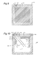
- the second layer of the package comprises two through-hole vias 1b1 and 1b2 on the left part of figure 9 .
- the through-hole vias 1b1 and 1b2 have exactly the same dimensions as the through-hole vias 1a1, 1a2 in the first layer, and when the first layer is located on top of the second layer the through-hole vias 1a1, 1a2 are exactly located above (aligned with) the through-hole vias 1b1, 1b2, respectively.
- the second layer comprises a ground structure 14a which covers most of the remaining area of the second layer apart from a plurality of through-hole vias 3b.
- These through-hole vias 3b have the same dimensions as through-hole vias 3a in the first layer (see figure 8 ) and will be aligned with through-hole vias 3a when the second layer is located on top of the first layer.
- the third layer of the package comprises a pair of stubs 2b1 and 2b2.
- the stub 2b1 comprises a long portion 2b12 and a short portion 2b11.
- the long portion 2b12 and the stub 2b2 are located on a central, non-conductive area of the third layer.
- the lengths of the stub 2b1 and 2b2 are substantially the same.
- the lengths of the stubs 2b1 and 2b2 equal one fourth of the wavelength ⁇ ( ⁇ / 4) of the signal transmitted from the die to the balun circuit 74 in order to short the unwanted second harmonic components of this signal as mentioned before.
- the 6 th , 10 th , etc. harmonic components may be shorted in this way as explained with reference to figure 7 .
- the third layer comprises three through-hole vias 1c1, 1c2.
- the through-hole vias 1c1, 1c2 have such dimensions and are arranged on such locations that they will be aligned with through-hole vias 1a1 and 1a2, 1b1 and 1b2, respectively, when the first and second layers are located on top of the third layer.
- the short portion 2b11 of stub 2b1 is connected to the through-hole via 1c1 and the stub 2b2 is connected to the through-hole via 1c2.
- the third layer comprises a plurality of through-hole vias 6, 8 which are located on the edge of the central, non-conductive area of the third layer.
- the third layer also has a plurality of through-hole vias 3c which are dimensioned and located to be aligned with through-hole vias 3b on the second layer when the first and second layers are located on top of the third layer.
- Both said stubs 2b1 and 2b2, and said vias 6, 8 are located inside of the same area as die attachment area 4 depicted in figure 8 .
- the fourth layer of the package comprises two conductive pads 1d1 and 1d2 on the upper-left part of the figure.
- the conductive pads 1d1 and 1d2, respectively, are located and arranged such that, when the first, second and third layers are located on top of the fourth layer, they connect to the through-hole vias 1c1 and 1c2, respectively. They are also connected to two short transmission lines 2c1 and 2c2, respectively, on the fourth layer that, on their other sides, are connected to suitable pads on the edge of the fourth layer.
- the two short transmission lines 2c1 and 2c2 are arranged such that, when the first, second and third layers are located on top of the fourth layer, they are aligned with the short transmission lines 2a1 and 2a2, respectively.
- the fourth layer comprises a plurality of conductive pads 3d that are located such that they are aligned with and connected to through-hole vias 3c in the third layer when the first, second and third layers are located on top of the fourth layer.
- the pads 3d are connected to suitable conductive leads 5b on the fourth layer that connect to a suitable pads 9b at the edge of the fourth layer.
- the fourth layer comprises a ground structure area 14c that substantially covers the remaining part of the area of the fourth layer. When the first, second and third layers are located on top of the fourth layer, the through-hole vias 6 in the third layer connect to the ground structure area 14c.
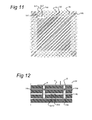
- figure 12 shows how the four layers are located relative to one another when they are located on top of one another.
- Figure 12 is a cross section along line XII-XII indicated in figure 10 .
- stub 2b1, together with transmission lines 2a1 and 2c1 act as one unified structure.
- stub 2b2, together with transmission lines 2a2 and 2c2 act as another unified structure. Both structures together provide the output of the die with the same impedance value as the pre-match circuit 72 that is depicted in figure 5 .
- the through-hole vias 6, 8 penetrate the package from the die attachment area 4 on the first layer to the fourth layer and is arranged to connect to the ground structure 14a on the second layer and to the ground structure 14c on the fourth layer.
- the aim of the through-hole via 6 is to electrically connect the die attachment area 4 to the ground structures 14a, and 14c.
- ground structure 14b is grounded too via one or more suitable through holes (not shown).
- the distances between the ground structures 14a, 14b and 14c, respectively, and the two structures are well defined. So, both unified structures together have a capacity against these ground structures 14a, 14b and 14c which is well defined and can be estimated very well in advance.
- a second embodiment of the package relates to a substrate of three-layers and will be explained with reference to figures 8 , 10 and 11 .
- the first layer is the same as the first layer of the first embodiment depicted in figure 8 .
- the second layer of the second embodiment is the same as the third layer of the first embodiment depicted in figure 10 .
- the third layer of the second embodiment is the same as the fourth layer of the first embodiment depicted in figure 11 .
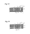
- figure 13 shows how, in the second embodiment, the three layers are located relative to one another when they are located on top of one another.
- Figure 13 is a cross section along line XII-XII indicated in figure 10 for the second embodiment.
- stub 2b1, together with transmission lines 2a1 and 2c1 act as one unified structure.
- stub 2b2, together with transmission lines 2a2 and 2c2 act as another unified structure. Both structures together provide the output of the die with the same impedance value as the pre-match circuit 72 that is depicted in figure 5 .
- the through-hole vias 6, 8 now penetrate the package from die attachment area 4 on the first layer to the second and third layer and is arranged to connect die attachment area 4 on the first layer to the ground structure 14c on the third layer.
- the aim of the through-hole via 6 is to electrically connect die attachment area 4 on the first layer to the ground structure 14c.
- ground structure 14b is grounded too via one or more suitable through holes (not shown).
- the distances between the first layer and the ground structures 14b and 14c, respectively, and the two structures are well defined. So, both unified structures together have a capacity against die attachment area 4 on the first layer and the ground structures 14b and 14c which are well defined and can be estimated very well in advance.
- a third embodiment of the package relates to a substrate of three-layers and will be explained with reference to figures 8 , 9 , 10 and 14 .
- the first layer is the same as the first layer of the first embodiment depicted in figure 8 .
- the second layer of the third embodiment is same as the second layer of the first embodiment depicted in figure 9 .
- the third layer of the third embodiment is same as the third layer of the first embodiment depicted in figure 10 .
- figure 14 shows how the three layer are located relative to one another when they are located on top of one another.
- Figure 14 is a cross section along line XII-XII indicated in figure 10 for the third embodiment.
- transmission line 2a1 and stub 2b1 act as one unified structure.
- transmission line 2a2 and stub 2b2 act as another unified structure. Both unified structures together provide the output of the die with the same impedance value as the pre-match circuit 72 that is depicted in figure 5 .
- the through-holes via 6, 8 penetrate the package from the die attachment area 4 on the first layer to the ground structure 14a to the bottom side of the third layer and is arranged to connect the first layer to the bottom of the third layer.
- the aim of the through-hole vias 6, 8 is to electrically connect the die attachment area 4 to the ground structure 14a and to the bottom of the third layer where it can be connected to a ground layer on the PCB.
- ground structure 14b is grounded too via one or more suitable through holes (not shown).
- the distances between the ground structures 14a, 14b and the ground layer on PCB below the third layer, respectively, and the two unified structures are well defined. So, both the unified structures together have a capacity against the ground structures 14a, 14b and the ground layer on the PCB which are well defined and can be estimated very well in advance.
- a fourth embodiment of the package relates to a substrate of two-layers and will be explained with reference to figures 8 , 10 and 15 .
- the first layer is the same as the first layer of the first embodiment depicted in figure 8 .
- the second layer of the fourth embodiment is the same as the third layer of the first embodiment depicted in figure 10 .
- figure 15 shows how the two layers are located relative to one another when they are located on top of one another.
- Figure 15 is a cross section along line XI-XI indicated in figure 10 for the fourth embodiment.
- transmission line 2a1 and stub 2b1 act as one unified structure.
- transmission line 2a2 and stub 2b2 act as another unified structure. Both unified structures together provide the output of the die with the same impedance value as the pre-match circuit 72 that is depicted in figure 5 .
- the through-hole vias 6, 8 are arranged to electrically connect the die attachment layer 4 to a ground layer on the PCB such that they are both grounded. Moreover, ground structure 14b is grounded too via one or more suitable through holes (not shown).
- the distances between the die attachment layer 4 and ground layer on PCB, respectively, and the two unified structures are well defined. So, both unified structures together have a capacity against the die attachment area 4, the ground structure 14b and the ground layer on the PCB which are well defined and can be estimated very well in advance.
- a fifth embodiment of the package relates to a substrate of four-layers and will be explained with reference to figure 8 , 9 , 11 and 16 . It is observed that this embodiment is not restricted to substrates with four layers. As a standard package, all four layers have the same dimension. As will be explained below, the four-layer package contains one or more stubs and a plurality of through-hole vias which together provide the same impedance as a pre-match circuit as shown in figure 4 , i.e. the pre-match circuit 72 is moved into package. The balun circuit 74 remains external (on main PCB).
- the first layer is the same as the first layer of the first embodiment depicted in figure 8 .
- the second layer of the fifth embodiment is the same as the second layer of the first embodiment depicted in figure 9 .
- the fourth layer of the fifth embodiment is the same as the fourth layer of the first embodiment depicted in figure 11 .
- Figure 16 shows the third layer of the fifth embodiment.
- the third layer of the package comprises a pair of stubs 2b1 and 2b2.
- the stub 2b1 comprises a long portion 2b12, a short portion 2b11, and an extended portion 2b 14 extending from the long portion 2b12.
- the stub 2b2 comprises a long portion 2b22, and an extended portion 2b24 extending from long portion 2b22.
- the stubs 2b1 and 2b2 are located on a central, non-conductive area of the third layer, respectively.
- the length of the long portion 2b22 equals the length of the short portion 2b1 together with long portion 2b12 of stub 2b1 which is one fourth of the wave length ⁇ ( ⁇ / 4) .
- the lengths of extended portions 2b14 of stub 2b1 and 2b24 of stub 2b2 are substantially the same. Their lengths are selected such as to short a certain further predetermined harmonic component of the signal. For instance, the lengths of 2b11+2b12 and of 2b22 are chosen such as to form a short for the second harmonic frequency at the location of vias 1c1 and 1c2, as explained above.
- the extended portions 2b14 and 2b24 have respective lengths that are selected such that together with the lengths of the portions of subs 2b1 and 2b2, respectively connecting the extending portions 2b14 and 2b24, respectively, to vias 1c1 and 1c2, respectively, form a short for the fourth (or other higher) harmonic at the locations of the vias 1c1 and 1c2.
- Available parameters for achieving both goals of providing a desired capacity for the pre-match circuit and of providing a short circuit for one or more higher harmonics are the length and width of 2b1 and 2b2, and, if present, of 2b14 and 2b24, respectively.
- the mutual couplings i.e. mutual distances, between the different stubs 2b1 / 2b2, 2b12 / 2b22 and between the stubs and the extended portions, so 2b14 / 2b12, 2b24 / 2b22 and between the stubs and extended portions and the ground planes (could be ground planes 14a, 14b or 14c or any combination thereof) can be used as a design parameter.
- extended portions 2b14 and 2b24 can be arranged such that they are substantially at an angle of 90 ° to each other and 45° to stubs 2b1 and 2b2, such they their mutual coupling to the stubs is negligible.
- layer three of the fifth embodiment as shown in figure 16 are the same as those of the third layer shown in figure 10 .
- figure 17 shows how the four layers are located relative to one another when they are located on top of one another.
- Figure 17 is a cross section along line XVII-XVII indicated in figure 16 .
- the cross section is essentially the same as the one shown in figure 12 , apart from the extended portions 2b14 and 2b24, respectively, on the third layer.
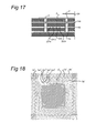
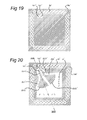
- a sixth embodiment of the new package relates to a substrate of four-layers and will be explained with reference to figure 18-21 . It is observed that this embodiment is not restricted to substrates with four layers.
- This package may use Surface Mount Technology (SMT) and wire bond attachment technology. As a standard package, all four layers have the same dimension.
- the four-layer package contains one or more stubs and a plurality of through-hole vias which together provide the same impedance as a pre-match circuit 72 as shown in figure 5 , i.e. the pre-match circuit 72 is moved into package.
- the balun circuit 74 remains external to the package but on main PCB.
- the first layer of the package comprises two through-hole vias 1a1' and 1a2' on the upper-left part of figure 18 . These through-hole vias 1a1', 1a2' are connected to two short transmission lines 2a1' and 2a2', respectively.
- the first layer comprises a big die attachment area 4' in the center where the chip (not shown in figure 18 ) is attached.
- the first layer comprises a plurality of pads 9a' consecutively located on the edges of figure 18 , a plurality of through-hole vias 3a' consecutively located close to said pads 9a', a pad 14' in the form of a circle located on the upper-left of figure 18 which is used as ground structure and connects to other ground structures (14a', 14b', 14c') on other layers by a through-hole via (not shown), a plurality of conducting leads 5a'. Each lead 5a' connects to both one pad 9a' and one through-hole via 3a'.
- Two wire bonds 16 (depicted in figure 22 ) are provided which connect to both said stubs 2a1' and 2a2' and the die attached above said attachment area 4'.
- the second layer of the package comprises two through-hole vias 1b1' and 1b2'. These two through-hole vias 1b1' and 1b2' have exactly the same dimensions as the two through-holes 1a1', 1a2' in the first layer, and when the first layer is located on top of the second layer the through-holes 1a1', 1a2' are exactly located above 1b1', 1b2', respectively.
- the second layer comprises a ground structure 14a' which covers most of the remaining area of the second layer apart from a plurality of through-holes 3b'. These through-holes 3b' have the same dimensions as through-holes 3a' in the first layer (see figure 18 ) and will be aligned with through-holes 3a' when the second layer is located on top of the first layer.
- the third layer of the package comprises two stubs 2b1' and 2b2'.
- Each of these stubs 2b1' and 2b2', respectively, comprise a short bar shaped area, 2b11' and 2b21', respectively.
- These bar shaped areas 2b11' and 2b21' may be aligned with the locations of stubs 2a1' and 2a2', respectively, on the first layer depicted in figure 18 .
- the stubs 2b1' and 2b2', respectively also comprise fan-shaped areas 2b12' and 2b22', respectively, which may be as large as one eighth of a circle area with a diameter of approximately 7mm.
- the third layer comprises two through-hole vias 1c1' and 1c2' which have such dimensions and are arranged on such locations that they will be aligned with through-holes 1a1' and 1a2', 1b1' and 1b2', respectively, when the first and second layers are located on top of the third layer.
- the third layer comprises a plurality of through-hole vias 6' which are symmetrically located on the edge of a central, non-conductive area of the third layer.
- the third layer also has a plurality of through-hole vias 3c' which are dimensioned and located to be aligned with through-hole vias 3b' on the second layer when the first and second layer are located on top of the third layer.
- Both said stubs 2b1' and 2b2', and said vias 6 are located inside of the same area as die attachment area 4 depicted in figure 18 .
- the third layer also comprises a ground structure 14b' which is located on the edge of figure 20 .
- the fourth layer of the package comprises two conductive pads 1d1' and 1d2' on the upper-left part of the figure.
- the conductive pads 1d1' and 1d2' respectively are located and arranged such that, when the first, second and third layers are located on top of the fourth layer, they connect to the through-hole vias 1c1' and 1c2', respectively. They are also connected to two short transmission lines 2c1' and 2c2', respectively, on the fourth layer that, on their other sides, are connected to suitable pads on the edge of the fourth layer.
- the two short transmission lines 2c1' and 2c2' are arranged such that, when the first, second and third layers are located on top of the fourth layer, they are aligned with the short transmission lines 1a1' and 1a2', respectively.
- the fourth layer comprises a plurality of conductive pads 3d' that are located such that they are aligned with and connected to through-holes 3c' in the third layer when the first, second and third layer are located on top of the fourth layer.
- the pads 3d' are connected to suitable conductive leads 5b' on the fourth layer that connect to suitable pads 9b' at the edge of the fourth layer.
- the fourth layer comprises a ground structure area 14c' that substantially covers the remaining part of the area of the fourth layer. When the first, second and third layers are located on top of the fourth layer, the through-hole vias 6' in the third layer connect to the ground structure area 14c'.
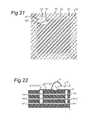
- figure 22 shows how the four layer are located relative to one another when they are located on top of one another.
- Figure 22 is a cross section along line XXII-XXII indicated in figure 20 .
- the through-hole vias 1a1', 1b1', 1c1' penetrate across the upper three layers where the first layer is the top layer and the fourth layer is the bottom layer.
- the last through-hole via 1c1' connects to pad 1d1' on the fourth layer.
- the through-hole vias 1a1', 1c1', 1d1', respectively, are attached to transmission line 2a1', stub 2b1' and transmission line 2c1', respectively.
- the through-hole vias 1a2', 1b2', 1c2' also penetrate across the upper three layers.
- the last through-hole via 1c2' connects to pad 1d2' on the fourth layer.
- the through-hole vias 1a2', 1c2', 1d2', respectively, are attached to transmission line 2a2', stub 2b2', and transmission line 2c2', respectively.
- stubs 2b1', transmission lines 2a1' and 2c1' act as one unified structure.
- stubs 2b2', transmission lines 2a2' and 2c2' act as another unified structure. Both structures together provide the output of the die with the same impedance value as the pre-match circuit 72 that is depicted in figure 5 .
- the through-hole via 6' penetrates the PCB from the first layer to the fourth layer and is arranged to electrically connect the ground structure 14a' on the second layer to the ground structure 14c' on the fourth layer.
- the distances between the ground structures 14', 14a', 14b' and 14c', respectively, and the fan shaped stubs 2b12', 2b22' are well defined. So, the two unified structures together have a capacity against these ground structures 14', 14a', 14b' and 14c' which is well defined and can be estimated very well in advance.
- two such ground structures are provided on opposing sides of the fan-shaped stubs 2b12', 2b22' they provide a cage of Faraday to the stubs, thus protecting from external electromagnetic radiation.
- the fan shaped structure can be combined with any one of the embodiments of the figures 8-17 .
Priority Applications (1)
| Application Number | Priority Date | Filing Date | Title |
|---|---|---|---|
| EP20100162427 EP2387295A1 (de) | 2010-05-10 | 2010-05-10 | IC-Packung mit integrierter Impedanzanpassung und harmonischer Unterdrückung |
Applications Claiming Priority (1)
| Application Number | Priority Date | Filing Date | Title |
|---|---|---|---|
| EP20100162427 EP2387295A1 (de) | 2010-05-10 | 2010-05-10 | IC-Packung mit integrierter Impedanzanpassung und harmonischer Unterdrückung |
Publications (1)
| Publication Number | Publication Date |
|---|---|
| EP2387295A1 true EP2387295A1 (de) | 2011-11-16 |
Family
ID=42732015
Family Applications (1)
| Application Number | Title | Priority Date | Filing Date |
|---|---|---|---|
| EP20100162427 Withdrawn EP2387295A1 (de) | 2010-05-10 | 2010-05-10 | IC-Packung mit integrierter Impedanzanpassung und harmonischer Unterdrückung |
Country Status (1)
| Country | Link |
|---|---|
| EP (1) | EP2387295A1 (de) |
Cited By (2)
| Publication number | Priority date | Publication date | Assignee | Title |
|---|---|---|---|---|
| WO2014013339A1 (en) * | 2012-07-16 | 2014-01-23 | Marvell World Trade Ltd. | Overcoming multiple reflections in packages and connectors at high speed broadband signal routing |
| EP4080677A1 (de) * | 2021-04-22 | 2022-10-26 | Nxp B.V. | Integriertes millimeterwellen-dual-modenanpassungsnetzwerk |
Citations (9)
| Publication number | Priority date | Publication date | Assignee | Title |
|---|---|---|---|---|
| US3662294A (en) * | 1970-05-05 | 1972-05-09 | Motorola Inc | Microstrip impedance matching circuit with harmonic terminations |
| US6215377B1 (en) | 1998-05-26 | 2001-04-10 | Microsubstrates Corporation | Low cost wideband RF port structure for microwave circuit packages using coplanar waveguide and BGA I/O format |
| US20040178854A1 (en) | 2003-03-14 | 2004-09-16 | Mitsubishi Denki Kabushiki Kaisha | Semiconductor device having balanced circuit for use in high frequency band |
| US20050151599A1 (en) * | 2004-01-08 | 2005-07-14 | Hitachi, Ltd. | Module for radio-frequency applications |
| US20060006938A1 (en) * | 2004-07-08 | 2006-01-12 | Lawrence Burns | Method and apparatus for an improved power amplifier |
| US20080191362A1 (en) | 2007-02-14 | 2008-08-14 | Advanced Semiconductor Engineering, Inc. | Semiconductor package having impedance matching device |
| US20080315392A1 (en) * | 2007-06-22 | 2008-12-25 | Cree, Inc. | Rf power transistor packages with internal harmonic frequency reduction and methods of forming rf power transistor packages with internal harmonic frequency reduction |
| US20090153261A1 (en) * | 2007-12-13 | 2009-06-18 | Ahmadreza Rofougaran | Method and system for matching networks embedded in an integrated circuit package |
| US20090212879A1 (en) * | 2008-02-25 | 2009-08-27 | Ahmadreza Rofougaran | Method and system for a balun embedded in an integrated circuit package |
-
2010
- 2010-05-10 EP EP20100162427 patent/EP2387295A1/de not_active Withdrawn
Patent Citations (9)
| Publication number | Priority date | Publication date | Assignee | Title |
|---|---|---|---|---|
| US3662294A (en) * | 1970-05-05 | 1972-05-09 | Motorola Inc | Microstrip impedance matching circuit with harmonic terminations |
| US6215377B1 (en) | 1998-05-26 | 2001-04-10 | Microsubstrates Corporation | Low cost wideband RF port structure for microwave circuit packages using coplanar waveguide and BGA I/O format |
| US20040178854A1 (en) | 2003-03-14 | 2004-09-16 | Mitsubishi Denki Kabushiki Kaisha | Semiconductor device having balanced circuit for use in high frequency band |
| US20050151599A1 (en) * | 2004-01-08 | 2005-07-14 | Hitachi, Ltd. | Module for radio-frequency applications |
| US20060006938A1 (en) * | 2004-07-08 | 2006-01-12 | Lawrence Burns | Method and apparatus for an improved power amplifier |
| US20080191362A1 (en) | 2007-02-14 | 2008-08-14 | Advanced Semiconductor Engineering, Inc. | Semiconductor package having impedance matching device |
| US20080315392A1 (en) * | 2007-06-22 | 2008-12-25 | Cree, Inc. | Rf power transistor packages with internal harmonic frequency reduction and methods of forming rf power transistor packages with internal harmonic frequency reduction |
| US20090153261A1 (en) * | 2007-12-13 | 2009-06-18 | Ahmadreza Rofougaran | Method and system for matching networks embedded in an integrated circuit package |
| US20090212879A1 (en) * | 2008-02-25 | 2009-08-27 | Ahmadreza Rofougaran | Method and system for a balun embedded in an integrated circuit package |
Cited By (4)
| Publication number | Priority date | Publication date | Assignee | Title |
|---|---|---|---|---|
| WO2014013339A1 (en) * | 2012-07-16 | 2014-01-23 | Marvell World Trade Ltd. | Overcoming multiple reflections in packages and connectors at high speed broadband signal routing |
| CN104603941A (zh) * | 2012-07-16 | 2015-05-06 | 马维尔国际贸易有限公司 | 克服高速宽带信号路由的封装和连接器中的多重反射 |
| CN104603941B (zh) * | 2012-07-16 | 2018-04-24 | 马维尔国际贸易有限公司 | 克服高速宽带信号路由的封装和连接器中的多重反射 |
| EP4080677A1 (de) * | 2021-04-22 | 2022-10-26 | Nxp B.V. | Integriertes millimeterwellen-dual-modenanpassungsnetzwerk |
Similar Documents
| Publication | Publication Date | Title |
|---|---|---|
| US9048232B2 (en) | Package with integrated pre-match circuit and harmonic suppression | |
| KR100703642B1 (ko) | 높은 양호도의 반응성 소자를 구비하는 집적 회로를 위한장치 및 방법 | |
| US7355491B2 (en) | Interconnecting a port of a microwave circuit package and a microwave component mounted in the microwave circuit package | |
| US6838953B2 (en) | High-frequency interconnection for circuits | |
| US6803252B2 (en) | Single and multiple layer packaging of high-speed/high-density ICs | |
| JPS61205001A (ja) | 伝送線路 | |
| US7613009B2 (en) | Electrical transition for an RF component | |
| US11937368B2 (en) | Structure for circuit interconnects | |
| JP2017163385A (ja) | 電子装置及び電子機器 | |
| US7154047B2 (en) | Via structure of packages for high frequency semiconductor devices | |
| US7291916B2 (en) | Signal transmission structure and circuit substrate thereof | |
| EP2387295A1 (de) | IC-Packung mit integrierter Impedanzanpassung und harmonischer Unterdrückung | |
| US11178765B2 (en) | Electronic device | |
| US7332799B2 (en) | Packaged chip having features for improved signal transmission on the package | |
| CN102544666B (zh) | 宽带非共面馈通 | |
| US20110084406A1 (en) | Device and interconnect in flip chip architecture | |
| CN210723306U (zh) | 慢波匹配电路和金丝键合慢波匹配结构 | |
| CN113678574B (zh) | 一种共模抑制的封装装置和印制电路板 | |
| JP2002185201A (ja) | 高周波用配線基板 | |
| CN218959175U (zh) | 多层基板模块 | |
| Rossi et al. | BGA Package for DDR3 Interface–4 vs 6 Layers Design Strategy and Electrical Performance Comparison | |
| US8975737B2 (en) | Transmission line for electronic circuits | |
| JP3833426B2 (ja) | 高周波用配線基板 | |
| Dittrich et al. | Characteristics and process stability of complete electrical interconnection structures for a low cost interposer technology | |
| WO2006019336A2 (en) | Impedance controlled interconnect substrate and package for high-frequency electronic device |
Legal Events
| Date | Code | Title | Description |
|---|---|---|---|
| AK | Designated contracting states |
Kind code of ref document: A1 Designated state(s): AL AT BE BG CH CY CZ DE DK EE ES FI FR GB GR HR HU IE IS IT LI LT LU LV MC MK MT NL NO PL PT RO SE SI SK SM TR |
|
| AX | Request for extension of the european patent |
Extension state: BA ME RS |
|
| PUAI | Public reference made under article 153(3) epc to a published international application that has entered the european phase |
Free format text: ORIGINAL CODE: 0009012 |
|
| 17P | Request for examination filed |
Effective date: 20120509 |
|
| 17Q | First examination report despatched |
Effective date: 20130419 |
|
| STAA | Information on the status of an ep patent application or granted ep patent |
Free format text: STATUS: THE APPLICATION IS DEEMED TO BE WITHDRAWN |
|
| 18D | Application deemed to be withdrawn |
Effective date: 20161201 |