EP2387294A2 - Verfahren und Vorrichtung zum Erhalt eines Stromflusswinkels, Verfahren und Vorrichtung zur Ansteuerung einer LED - Google Patents
Verfahren und Vorrichtung zum Erhalt eines Stromflusswinkels, Verfahren und Vorrichtung zur Ansteuerung einer LED Download PDFInfo
- Publication number
- EP2387294A2 EP2387294A2 EP11157848A EP11157848A EP2387294A2 EP 2387294 A2 EP2387294 A2 EP 2387294A2 EP 11157848 A EP11157848 A EP 11157848A EP 11157848 A EP11157848 A EP 11157848A EP 2387294 A2 EP2387294 A2 EP 2387294A2
- Authority
- EP
- European Patent Office
- Prior art keywords
- dimmer
- conduction angle
- trailing edge
- edge dimmer
- time point
- Prior art date
- Legal status (The legal status is an assumption and is not a legal conclusion. Google has not performed a legal analysis and makes no representation as to the accuracy of the status listed.)
- Granted
Links
- 238000000034 method Methods 0.000 title claims abstract description 59
- 230000008859 change Effects 0.000 claims description 11
- 238000005070 sampling Methods 0.000 claims description 10
- 238000012935 Averaging Methods 0.000 claims description 2
- 238000010586 diagram Methods 0.000 description 9
- 238000002955 isolation Methods 0.000 description 9
- 230000008569 process Effects 0.000 description 6
- 238000001514 detection method Methods 0.000 description 4
- 239000003990 capacitor Substances 0.000 description 3
- 230000003247 decreasing effect Effects 0.000 description 3
- 208000032365 Electromagnetic interference Diseases 0.000 description 2
- 230000008901 benefit Effects 0.000 description 2
- 230000007423 decrease Effects 0.000 description 2
- 238000004519 manufacturing process Methods 0.000 description 2
- 230000033228 biological regulation Effects 0.000 description 1
- 230000008878 coupling Effects 0.000 description 1
- 238000010168 coupling process Methods 0.000 description 1
- 238000005859 coupling reaction Methods 0.000 description 1
- 238000012986 modification Methods 0.000 description 1
- 230000004048 modification Effects 0.000 description 1
- 230000003287 optical effect Effects 0.000 description 1
Images



Classifications
-
- H—ELECTRICITY
- H05—ELECTRIC TECHNIQUES NOT OTHERWISE PROVIDED FOR
- H05B—ELECTRIC HEATING; ELECTRIC LIGHT SOURCES NOT OTHERWISE PROVIDED FOR; CIRCUIT ARRANGEMENTS FOR ELECTRIC LIGHT SOURCES, IN GENERAL
- H05B45/00—Circuit arrangements for operating light-emitting diodes [LED]
- H05B45/30—Driver circuits
- H05B45/37—Converter circuits
- H05B45/3725—Switched mode power supply [SMPS]
- H05B45/382—Switched mode power supply [SMPS] with galvanic isolation between input and output
-
- Y—GENERAL TAGGING OF NEW TECHNOLOGICAL DEVELOPMENTS; GENERAL TAGGING OF CROSS-SECTIONAL TECHNOLOGIES SPANNING OVER SEVERAL SECTIONS OF THE IPC; TECHNICAL SUBJECTS COVERED BY FORMER USPC CROSS-REFERENCE ART COLLECTIONS [XRACs] AND DIGESTS
- Y02—TECHNOLOGIES OR APPLICATIONS FOR MITIGATION OR ADAPTATION AGAINST CLIMATE CHANGE
- Y02B—CLIMATE CHANGE MITIGATION TECHNOLOGIES RELATED TO BUILDINGS, e.g. HOUSING, HOUSE APPLIANCES OR RELATED END-USER APPLICATIONS
- Y02B20/00—Energy efficient lighting technologies, e.g. halogen lamps or gas discharge lamps
- Y02B20/30—Semiconductor lamps, e.g. solid state lamps [SSL] light emitting diodes [LED] or organic LED [OLED]
Definitions
- the present invention relates to method and device for obtaining a conduction angle of a trailing edge dimmer. Further, the present invention relates to a method and device for driving an LED.
- the phase control dimmer mainly includes a leading edge dimmer and a trailing edge dimmer.
- Figure 1 shows respectively a common connection method of the dimmer in the prior art and an ideal output waveform of the dimmer.
- LED driving device With respect to an LED device, it cannot be connected to a mains supply network directly as an incandescent lamp, and thus the traditional dimmer cannot be directly used for dimming. Instead, a switching power supply needs to be used as a DC driving device for the LED device. Thus, it is desired that such LED driving device can be compatible with the traditional dimmer.
- a method for obtaining a conduction angle of a trailing edge dimmer comprising: determining a time point t0 when the trailing edge dimmer starts to be conductive; determining an earliest time point t1 when a deviation from an ideal waveform appears; and determining the conduction angle t1-t0 of the trailing edge dimmer based on the earliest time point t1 when the deviation from the ideal waveform appears and the time point t0 when the trailing edge dimmer starts to be conductive.
- the conduction angle of the trailing edge dimmer can be effectively determined, so that LED can be dimmed according to the conduction angle of the trailing edge dimmer, and an influence of the random interference can be reduced.
- an LED driving method comprising: determining a type of a dimmer; obtaining a conduction angle of a leading edge dimmer, when it is determined that the dimmer connected is the leading edge dimmer; obtaining a conduction angle of a trailing edge dimmer with above method, when it is determined that the dimmer connected is the trailing edge dimmer; and generating a dimming signal according to the obtained conduction angle of the dimmer.
- a conduction angle obtaining device for a trailing edge dimmer comprising: a conducting time point determining unit, which is configured to determine a time point t0 when the trailing edge dimmer starts to be conductive; a phase cutting point determining unit, which is configured to determine an earliest time point t1 when a deviation from an ideal waveform appears; and a conduction angle determining unit, which is configured to determine the conduction angle t1-t0 of the trailing edge dimmer based on the earliest time point t1 when the deviation from the ideal waveform appears and the time point t0 when the trailing edge dimmer starts to be conductive.
- the conduction angle of the trailing edge dimmer can be effectively determined, so as to perform dimming on the LED according to the conduction angle of the trailing edge dimmer. Further, the influence of the random interference can be reduced.
- an LED driving device comprising: a dimmer type determining unit, which is configured to determine a type of a dimmer; a conduction angle obtaining device for a leading edge dimmer, which is configured to obtain a conduction angle of a leading edge dimmer, when it is determined that the dimmer connected is the leading edge dimmer; a conduction angle obtaining device for a trailing edge dimmer as described above, which is configured to obtain a conduction angle of a trailing edge dimmer, when it is determined that the dimmer connected is the trailing edge dimmer; and a dimming unit, which is configured to generate a dimming signal according to the obtained conduction angle of the dimmer.
- the LED driving device compatibility with the leading edge dimmer and the trailing edge dimmer can be effectively achieved, and the LED can be dimmed according to the conduction angle of the phase dimmer. Moreover, the influence of the random interference can be reduced, and the flickering of the LED caused by the jittering of the dimmer can be eliminated.
- an LED driving method comprising: generating a PWM control signal with a PWM dimming signal; and controlling a PWM DC/DC converter with the PWM control signal, so as to generate a driving voltage of the LED.
- the PWM dimming can be utilized, and meanwhile an effective isolation between the LED device and the high voltage power supply can be ensured.
- an LED driving system comprising: a PWM DC/DC converter, a PWM controller and a PWM dimming signal generating unit; wherein: the PWM dimming signal generating unit is configured to generate a PWM dimming signal; the PWM controller is configured to generate a PWM control signal by utilizing the PWM dimming signal; and the PWM DC/DC converter is configured to generate a driving voltage of LED according to the PWM control signal.
- the PWM dimming can be utilized, and meanwhile an effective isolation between the LED device and the high voltage power supply can be ensured, so that it is guaranteed that the system can easily be designed in conformity with the security standard.
- the system has a simple structure, so that the production cost is greatly reduced, and a precise constant current character can be ensured.
- the high precision requirements regarding the current of LED can be met.
- Figure 1 shows a common connection method of the dimmer in the prior art and an ideal output waveform of the dimmer
- Figure 2 shows an example waveform of a rectified output voltage of the trailing edge dimmer
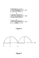
- Figure 3 shows a flow chart of the method for obtaining the conduction angle of the trailing edge dimmer according to an embodiment of the invention
- Figure 4 shows an example waveform of a rectified output voltage of the leading edge dimmer
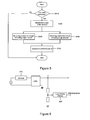
- Figure 5 shows a flow chart of the method for driving LED that can be compatible with the leading edge dimmer and the trailing edge dimmer;
- Figure 6 shows a principle diagram for dimmer detection
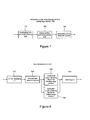
- Figure 7 shows a schematic block diagram of a conduction angle obtaining device for the trailing edge dimmer according to an embodiment of the invention
- Figure 8 shows a block diagram of an LED driving device that can be compatible with the leading edge dimmer and the trailing edge dimmer according to an embodiment of the invention
- Figure 9 schematically shows the principle of the linear dimming
- FIG. 10 schematically shows the principle of the PWM dimming
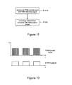
- Figure 11 shows a flow chart of the method for driving LED according to an embodiment of the invention
- Figure 12 schematically shows the waveform of the generated PWM control signal
- Figure 13 shows a schematic structural diagram of an LED driving system according to an embodiment of the invention.
- a capacitor whose typical value is 100nF-150nF is generally connected with the output terminal of the trailing edge dimmer in parallel.
- the Electro-Magnetic Interference (EMI) filter on the input terminal of the LED driver generally also comprises a capacitor. These capacitors may cause that the output voltage of the dimmer cannot decrease rapidly as in the ideal waveform.
- Figure 2 shows an example waveform of a rectified output voltage of the trailing edge dimmer. As shown in Figure 2 , before starting of another cycle, the voltage is decreased to zero after a relatively long time period.
- the time point t2 when the output voltage of the dimmer is decreased to zero cannot reflect the conduction angle of the dimmer correctly, which may cause that the LED lamp cannot be dimmed correctly or that the dimmable range is fairly narrow. This is the reason why there is no dimmable LED lamp available on the market that can practically be compatible with the trailing edge dimmer.
- the inventor notices that, as shown in Figure 2 , after the phase cutting of the trailing edge dimmer, although the voltage cannot be decreased to zero quickly, a certain difference exists between the waveform thereof and the ideal waveform. Therefore, if the earliest time point t1 when a deviation from the ideal waveform appears can be determined, it can be deemed that the trailing edge dimmer performs the phase cutting at this time point. Thus, it can be determined that the conduction angle of the trailing edge dimmer is t1-t0, wherein t0 is the time point when the trailing edge dimmer starts to be conductive.
- Figure 3 shows the flow chart of this method. As shown in Figure 3 , the method comprises following steps:
- S310 determining a time point t0 when the trailing edge dimmer starts to be conductive. After the time point t0, the trailing edge dimmer starts to be conductive, thus the output voltage thereof should be substantially the same as the ideal waveform.
- the ideal waveform is assumed to be a sinus wave in Figure 2 . Thus, in the conductive phase of the trailing edge dimmer starting from the time point t0, the output voltage is substantially the same as the sinus wave.
- step S320 determining an earliest time point t1 when a deviation from an ideal waveform appears. Specifically, in step S320, a sampling can be performed on the output voltage of the trailing edge dimmer, the sampled values are compared with the ideal waveform, and the earliest time point t1 when the deviation from the ideal waveform appears is determined based on the difference between the output voltage and the ideal waveform. When the time point t1 is determined, the time point t1 is considered to be the phase cutting point of the trailing edge dimmer.
- S330 determining the conduction angle t1-t0 of the trailing edge dimmer based on the earliest time point t1 when the deviation from the ideal waveform appears and the time point t0 when the trailing edge dimmer starts to be conductive.
- the LED can be dimmed according to the determined conduction angle.
- a PWM (Pulse Width Modulation) signal can be generated according to the conduction angle of the dimmer, wherein the duty cycle of the PWM signal is relevant to the conduction angle of the dimmer, and the PWM signal is used for the regulation of the LED brightness.
- a linear dimming is performed according to the conduction angle of the dimmer, which can be easily conceived by those skilled in the art.
- the LED driving device is not a resistance load, there may exist a situation that the matching between the LED driving device and the dimmer is not particularly ideal. In this situation the output of the LED driving device may has a random interference, so that a flickering of the LED lamp may be easily caused. For this situation, it is preferred to calculate an average value of the conduction angles obtained in a plurality of cycles during the detecting process of the conduction angle of the dimmer and perform dimming on the LED according to the average value, so as to reduce the influence of the random interference.
- the conduction angle of the trailing edge dimmer can be effectively determined, so as to perform dimming on the LED according to the conduction angle of the trailing edge dimmer. Further, the influence of the random interference can be reduced.
- the traditional dimmer includes the leading edge dimmer and the trailing edge dimmer. Therefore, according to an embodiment of the invention, there is provided a method for driving an LED that can be compatible with the leading edge dimmer and the trailing edge dimmer.
- Figure 4 shows an example waveform of a rectified output voltage of the leading edge dimmer.
- the output voltage of the leading edge dimmer is substantially zero.
- the leading edge dimmer becomes conductive, so that a jump appears in the output voltage.
- the output voltage decreases to zero according to the standard voltage.
- This method for obtaining the conduction angle of the leading edge dimmer is familiar to those skilled in the art and will not be illustrated in detail here.
- Figure 5 shows a flow chart of the method for driving LED that can be compatible with the leading edge dimmer and the trailing edge dimmer. As shown in Figure 5 , the method comprises following steps:
- FIG. 6 can be referred to, where a principle diagram for dimmer detection is schematically illustrated.
- an LED driving device 620 performs sampling and analysis for the voltage on point A at a certain sampling rate through a resistance voltage divider.
- the LED driving device 620 compares the sampled voltage with a reference voltage.
- the reference voltage may be already stored in the LED driving device 620, or may be input from external.
- the LED driving device 620 can analyze the time when the sampled voltage is larger than and smaller than the reference voltage, and take such time information as a criterion to determine whether a dimmer is connected. It can be readily conceived by those skilled in the art that the LED driving device can be implemented with a micro-controller such as MCU or DSP.
- step S510 is optional.
- a dimmer is connected, so that the subsequent steps are implemented directly.
- S520 determining a type of the dimmer when it is determined that the dimmer is connected. It can be seen from Figure 1 that the output waveform of the leading edge dimmer is obviously different from that of the trailing edge dimmer. Thus, the type of the dimmer can be determined according to the sampled signals.
- the conduction angle of the leading edge dimmer is obtained with the method for obtaining the conduction angle of the leading edge dimmer as described above.
- the conduction angle of the trailing edge dimmer is obtained with the method for obtaining the conduction angle of the trailing edge dimmer as described in the first embodiment of the invention.
- step S550 a dimming signal is generated according to the obtained conduction angle.
- an anti-jittering control step is comprised after the conduction angle of the dimmer is obtained.
- the change in the conduction angle of the dimmer is detected, and only when the change in the conduction angle of the dimmer is larger than a certain threshold value, the dimming signal is generated in the dimming step according to the changed conduction angle of the dimmer.
- compatibility with the leading edge dimmer and the trailing edge dimmer can be effectively achieved, and the LED can be dimmed according to the conduction angle of the phase dimmer. Moreover, the influence of the random interference can be reduced, and the flickering of the LED caused by the jittering of the dimmer can be eliminated.
- the third embodiment of the invention corresponds to the above first embodiment, where a conduction angle obtaining device for the trailing edge dimmer 700 is described.
- Figure 7 shows a schematic block diagram of the conduction angle obtaining device for the trailing edge dimmer 700 according to the third embodiment of the invention.
- the conduction angle obtaining device for the trailing edge dimmer 700 comprises:
- a conducting time point determining unit 710 which is configured to determine a time point t0 when the trailing edge dimmer starts to be conductive. After the time point t0, the trailing edge dimmer starts to be conductive, thus the output voltage thereof should be substantially the same as the ideal waveform.
- the ideal waveform is assumed to be a sinus wave in Figure 2 . Thus, in the conductive phase of the trailing edge dimmer starting from the time point t0, the output voltage is substantially the same as the sinus wave.
- a phase cutting point determining unit 720 which is configured to determine an earliest time point t1 when a deviation from an ideal waveform appears.
- the phase cutting point determining unit 720 can further comprise a sampling device and a comparing device, wherein the sampling device is configured to perform a sampling on the output voltage of the trailing edge dimmer to obtain sampled values, and the comparing device is configured to compare the sampled values with the ideal waveform, and determine the earliest time point t1 when the deviation from the ideal waveform appears based on the difference between the output voltage and the ideal waveform.
- the time point t1 is considered to be the phase cutting point of the trailing edge dimmer.
- a conduction angle determining unit 730 which is configured to determine the conduction angle t1-t0 of the trailing edge dimmer based on the earliest time point t1 when the deviation from the ideal waveform appears and the time point t0 when the trailing edge dimmer starts to be conductive.
- the conduction angle determining unit 730 may further comprises a averaging device, which is configured to calculate an average value of the conduction angles obtained in a plurality of cycles during the detecting process of the conduction angle of the dimmer, and take the average value as the finally obtained conduction angle, so as to reduce the influence of the random interference.
- the conduction angle of the trailing edge dimmer can be effectively determined, so as to perform dimming on the LED according to the conduction angle of the trailing edge dimmer. Further, the influence of the random interference can be reduced.
- the fourth embodiment of the invention corresponds to the above second embodiment, where an LED driving device 800 that is compatible with the leading edge dimmer and the trailing edge dimmer is described.
- FIG. 8 shows a block diagram of an LED driving device that can be compatible with the leading edge dimmer and the trailing edge dimmer according to the embodiment of the invention.
- the LED driving device 800 comprises following modules:
- a dimmer detecting unit 810 which is configured to detect whether a dimmer is connected.
- Figure 6 can be referred to, where a principle diagram for dimmer detection is schematically illustrated. Please refer to the description in the second embodiment for the detailed procedure for dimmer detection, which will not be described again here.
- the dimmer detecting unit 810 is optional in the LED driving device 800.
- a dimmer type determining unit 820 which is configured to determine a type of the dimmer when it is determined that the dimmer is connected. It can be seen from Figure 1 that the output waveform of the leading edge dimmer is obviously different from that of the trailing edge dimmer. Thus, the dimmer type determining unit 820 can determine the type of the dimmer according to the sampled signals.
- a conduction angle obtaining device for the leading edge dimmer 830 which is configured to obtain the conduction angle of the leading edge dimmer with the method for detecting the conduction angle of the leading edge dimmer, when it is determined that the connected dimmer is a leading edge dimmer.
- a conduction angle obtaining device for the trailing edge dimmer 700 as described in the third embodiment of the invention which is configured to obtain the conduction angle of the trailing edge dimmer when it is determined that the connected dimmer is a trailing edge dimmer.
- a dimming unit 850 which is configured to generate a dimming signal according to the obtained conduction angle.
- the conduction angle obtaining device for the leading edge dimmer 830 and the conduction angle obtaining device for the trailing edge dimmer 700 are configured to calculate an average value of the conduction angles obtained in a plurality of cycles, so that the dimming unit 850 can perform dimming on the LED according to the average value, so as to reduce the influence of the random interference.
- the LED driving device 800 comprises an anti-jittering control unit (not shown), which is configured to detect the change in the conduction angle of the dimmer, and only when the change in the conduction angle of the dimmer is larger than a certain threshold value, the dimming signal is generated according to the changed conduction angle of the dimmer.
- an anti-jittering control unit (not shown), which is configured to detect the change in the conduction angle of the dimmer, and only when the change in the conduction angle of the dimmer is larger than a certain threshold value, the dimming signal is generated according to the changed conduction angle of the dimmer.
- the LED driving device 800 compatibility with the leading edge dimmer and the trailing edge dimmer can be effectively achieved, and the LED can be dimmed according to the conduction angle of the phase dimmer. Moreover, the influence of the random interference can be reduced, and the flickering of the LED caused by the jittering of the dimmer can be eliminated.
- FIG. 10 schematically shows the principle of the PWM dimming. As can be seen from Figure 10 , during the conduction of LED, the magnitude of the current flowing through LED maintains unchanged, and thus a relatively high light-emitting efficiency and a good light-emitting quality can be achieved.
- a DC voltage is required to drive the LED, it is known to those skilled in the art the isolate the LED device from the high voltage power supply with a DC/DC converter.
- a PWM control signal is output by the PWM controller to control the switching of the DC/DC converter, so that the voltage from the power supply becomes a high frequency pulse, and thus can be converted by the converter into a low voltage for driving the LED.
- the frequency of the PWM control signal is in the order of ten kilohertz (kHz) to hundred kilohertz.
- the frequency of the PWM dimming signal that is used to perform PWM dimming for the LED is generally in the range from 100Hz to 1000Hz, which is much lower than that of the PWM control signal.
- the PWM dimming signal is modulated to the present PWM control signal directly, i.e., when an amplitude modulation is performed on the present PWM control signal by utilizing the PWM dimming signal to generate a new PWM control signal, the dimming signal can be directly carried by the new PWM control signal, so that the structure of the system can be greatly simplified.
- the PWM control signal here can be generated by performing an amplitude modulation on the present PWM control signal, or can be generated by performing a frequency modulation on the PWM dimming signal. Further, it can be deemed that the PWM signal in the invention is generated directly according to the PWM dimming signal, i.e., the envelope curve of the high frequency PWM control signal generated is in conformity to the waveform of the PWM dimming signal.
- Figure 11 shows a flow chart of the method for driving LED. As can be seen from the drawing, the method comprises following steps:
- S1110 generating a PWM control signal with the PWM dimming signal.
- the frequency of the PWM dimming signal is generally in the range from 100Hz to 1000Hz.
- Figure 12 schematically shows the generated PWM control signal.
- the envelope curve of the new PWM control signal changes according to the PWM dimming signal.
- the original PWM control signal is still included. In other words, an amplitude/frequency modulation is performed on the original PWM control signal with the PWM dimming signal, and the frequency of the PWM control signal is not changed.
- S1120 controlling the PWM DC/DC converter with the PWM control signal, so as to generate a driving voltage of the LED.
- the PWM dimming can be utilized, and meanwhile an effective isolation between the LED device and the high voltage power supply can be ensured.
- an LED driving system is provided, which can realize the utilization of the PWM dimming and the effective isolation.
- FIG. 13 shows a schematic structural diagram of the LED driving system according to an embodiment of the invention.
- the LED driving system comprises: a PWM DC/DC converter 1310, a PWM controller 1320 and a PWM dimming signal generating unit 1330.
- the PWM dimming signal generating unit 1330 is configured to generate the PWM dimming signal.
- the PWM controller 1320 is configured to generate the PWM control signal by utilizing the PWM dimming signal.
- the frequency of the PWM dimming signal is generally in the range from 100Hz to 1000Hz.
- the PWM DC/DC converter 1310 is configured to generate the driving voltage of LED according to the PWM control signal.
- the LED driving system further comprises a constant current control unit 1340, which is adapted to ensure that the magnitude of the current flowing through the LED maintains constant.
- the operation principle of the constant current control unit 1340 is that the current flowing through the LED is detected and compared with a predefined value. When the current of the LED is different from the predefined value, a feedback signal is generated to the PWM controller 1320 for adjusting the PWM control signal.
- the operation mode is familiar to those skilled in the art, and will not be further illustrated here.
- the LED driving system according to the embodiment further comprises an isolation and feedback unit 1350, which is configured to input the feedback signal from the constant current control unit 1340 to the PWM controller in an electrical isolation manner.
- an optical coupling can be employed to achieve the isolation.
- the PWM dimming can be utilized, and meanwhile an effective isolation between the LED device and the high voltage power supply can be ensured, so that it is guaranteed that the system can easily be designed in conformity with the security standard.
- the system has a simple structure, so that the production cost is greatly reduced, and a precise constant current character can be ensured.
- the high precision requirements regarding the current of LED can be met.
- the term “include”, “comprise” or any other variations means a non-exclusive inclusion, so that the process, method, article or device that includes a series of elements includes not only these elements but also other elements that are not explicitly listed, or further includes inherent elements of the process, method, article or device. Moreover, when there is no further limitation, the element defined by the wording "comprise(s) a " does not exclude the case that in the process, method, article or device that includes the element there are other same elements.
Landscapes
- Circuit Arrangement For Electric Light Sources In General (AREA)
- Led Devices (AREA)
Applications Claiming Priority (1)
| Application Number | Priority Date | Filing Date | Title |
|---|---|---|---|
| CN201010168705.6A CN102238774B (zh) | 2010-04-30 | 2010-04-30 | 导通角获取方法和装置,以及led驱动方法和装置 |
Publications (3)
| Publication Number | Publication Date |
|---|---|
| EP2387294A2 true EP2387294A2 (de) | 2011-11-16 |
| EP2387294A3 EP2387294A3 (de) | 2012-04-25 |
| EP2387294B1 EP2387294B1 (de) | 2014-06-11 |
Family
ID=44475163
Family Applications (1)
| Application Number | Title | Priority Date | Filing Date |
|---|---|---|---|
| EP11157848.0A Active EP2387294B1 (de) | 2010-04-30 | 2011-03-11 | Verfahren und Vorrichtung zum Erhalt eines Stromflusswinkels, Verfahren und Vorrichtung zur Ansteuerung einer LED |
Country Status (3)
| Country | Link |
|---|---|
| US (1) | US8558477B2 (de) |
| EP (1) | EP2387294B1 (de) |
| CN (1) | CN102238774B (de) |
Cited By (3)
| Publication number | Priority date | Publication date | Assignee | Title |
|---|---|---|---|---|
| CN103575956A (zh) * | 2012-07-27 | 2014-02-12 | 东芝照明技术株式会社 | 检测电路及检测方法 |
| EP2938163A1 (de) * | 2014-04-22 | 2015-10-28 | Power Integrations, Inc. | Dimmungsgrenzendetektion für leistungswandler |
| WO2016077181A1 (en) * | 2014-11-10 | 2016-05-19 | Power Integrations, Inc. | Phase angle detection module for power converter |
Families Citing this family (61)
| Publication number | Priority date | Publication date | Assignee | Title |
|---|---|---|---|---|
| US7667408B2 (en) | 2007-03-12 | 2010-02-23 | Cirrus Logic, Inc. | Lighting system with lighting dimmer output mapping |
| US7288902B1 (en) | 2007-03-12 | 2007-10-30 | Cirrus Logic, Inc. | Color variations in a dimmable lighting device with stable color temperature light sources |
| US8212491B2 (en) | 2008-07-25 | 2012-07-03 | Cirrus Logic, Inc. | Switching power converter control with triac-based leading edge dimmer compatibility |
| US9155174B2 (en) | 2009-09-30 | 2015-10-06 | Cirrus Logic, Inc. | Phase control dimming compatible lighting systems |
| US8729811B2 (en) | 2010-07-30 | 2014-05-20 | Cirrus Logic, Inc. | Dimming multiple lighting devices by alternating energy transfer from a magnetic storage element |
| US8947016B2 (en) | 2010-07-30 | 2015-02-03 | Cirrus Logic, Inc. | Transformer-isolated LED lighting circuit with secondary-side dimming control |
| US8716957B2 (en) | 2010-07-30 | 2014-05-06 | Cirrus Logic, Inc. | Powering high-efficiency lighting devices from a triac-based dimmer |
| US8536799B1 (en) * | 2010-07-30 | 2013-09-17 | Cirrus Logic, Inc. | Dimmer detection |
| US8569972B2 (en) | 2010-08-17 | 2013-10-29 | Cirrus Logic, Inc. | Dimmer output emulation |
| US9307601B2 (en) | 2010-08-17 | 2016-04-05 | Koninklijke Philips N.V. | Input voltage sensing for a switching power converter and a triac-based dimmer |
| WO2012027507A2 (en) | 2010-08-24 | 2012-03-01 | Cirrus Logic, Inc. | Multi-mode dimmer interfacing including attach state control |
| WO2012061454A2 (en) | 2010-11-04 | 2012-05-10 | Cirrus Logic, Inc. | Duty factor probing of a triac-based dimmer |
| CN103270678B (zh) | 2010-11-04 | 2016-10-12 | 皇家飞利浦有限公司 | 切换功率转换器输入电压近似过零点确定 |
| US9497851B2 (en) | 2010-11-04 | 2016-11-15 | Koninklijke Philips N.V. | Thermal management in a lighting system using multiple, controlled power dissipation circuits |
| WO2012061769A2 (en) | 2010-11-04 | 2012-05-10 | Cirrus Logic, Inc. | Controlled power dissipation in a switch path in a lighting system |
| ES2718100T3 (es) | 2010-11-16 | 2019-06-27 | Signify Holding Bv | Compatibilidad de atenuador de luz de fase final con predicción de alta resistencia de atenuador de luz |
| EP2653014B1 (de) | 2010-12-16 | 2016-10-19 | Philips Lighting Holding B.V. | Übergänge zwischen dem discontinuous mode und dem critical conduction mode in abhängigkeit eines schaltparameters |
| CN103108435B (zh) * | 2011-11-14 | 2017-05-24 | 欧司朗股份有限公司 | 阻尼电路、led驱动器以及led照明系统 |
| EP2792059B1 (de) | 2011-12-14 | 2020-07-15 | Signify Holding B.V. | Isolierung eines sekundären transformatorwicklungsstroms während der erzeugung von hilfsstrom |
| EP2810532B1 (de) | 2012-02-01 | 2019-05-22 | Signify Holding B.V. | Treibervorrichtung und treiberverfahren zum antreiben einer last, insbesondere in einer led-einheit mit einer oder mehreren leds |
| EP2810533B1 (de) | 2012-02-02 | 2015-08-05 | Koninklijke Philips N.V. | Led-lichtquelle |
| US9167662B2 (en) | 2012-02-29 | 2015-10-20 | Cirrus Logic, Inc. | Mixed load current compensation for LED lighting |
| CN102612227B (zh) * | 2012-03-09 | 2014-02-12 | 矽力杰半导体技术(杭州)有限公司 | 一种混合调光电路及其混合调光方法 |
| US9072125B2 (en) | 2012-07-03 | 2015-06-30 | Cirrus Logic, Inc. | Systems and methods for determining a type of transformer to which a load is coupled |
| US9215770B2 (en) | 2012-07-03 | 2015-12-15 | Philips International, B.V. | Systems and methods for low-power lamp compatibility with a trailing-edge dimmer and an electronic transformer |
| US9184661B2 (en) | 2012-08-27 | 2015-11-10 | Cirrus Logic, Inc. | Power conversion with controlled capacitance charging including attach state control |
| US9277624B1 (en) | 2012-10-26 | 2016-03-01 | Philips International, B.V. | Systems and methods for low-power lamp compatibility with an electronic transformer |
| CN103024994B (zh) | 2012-11-12 | 2016-06-01 | 昂宝电子(上海)有限公司 | 使用triac调光器的调光控制系统和方法 |
| US9273858B2 (en) | 2012-12-13 | 2016-03-01 | Phillips International, B.V. | Systems and methods for low-power lamp compatibility with a leading-edge dimmer and an electronic transformer |
| US9496844B1 (en) | 2013-01-25 | 2016-11-15 | Koninklijke Philips N.V. | Variable bandwidth filter for dimmer phase angle measurements |
| US9263964B1 (en) | 2013-03-14 | 2016-02-16 | Philips International, B.V. | Systems and methods for low-power lamp compatibility with an electronic transformer |
| US10187934B2 (en) | 2013-03-14 | 2019-01-22 | Philips Lighting Holding B.V. | Controlled electronic system power dissipation via an auxiliary-power dissipation circuit |
| US9282598B2 (en) | 2013-03-15 | 2016-03-08 | Koninklijke Philips N.V. | System and method for learning dimmer characteristics |
| CN105359624B (zh) * | 2013-05-13 | 2017-09-29 | 飞利浦照明控股有限公司 | 电路稳定装置和方法 |
| US9635723B2 (en) | 2013-08-30 | 2017-04-25 | Philips Lighting Holding B.V. | Systems and methods for low-power lamp compatibility with a trailing-edge dimmer and an electronic transformer |
| CN103747569B (zh) | 2013-12-25 | 2015-11-25 | 矽力杰半导体技术(杭州)有限公司 | 一种pwm调光控制方法、控制电路及应用其的led驱动电路 |
| US9621062B2 (en) | 2014-03-07 | 2017-04-11 | Philips Lighting Holding B.V. | Dimmer output emulation with non-zero glue voltage |
| US9277611B2 (en) * | 2014-03-17 | 2016-03-01 | Terralux, Inc. | LED driver with high dimming compatibility without the use of bleeders |
| US9215772B2 (en) | 2014-04-17 | 2015-12-15 | Philips International B.V. | Systems and methods for minimizing power dissipation in a low-power lamp coupled to a trailing-edge dimmer |
| CN103957634B (zh) * | 2014-04-25 | 2017-07-07 | 广州昂宝电子有限公司 | 照明系统及其控制方法 |
| US9385598B2 (en) | 2014-06-12 | 2016-07-05 | Koninklijke Philips N.V. | Boost converter stage switch controller |
| CN104020377A (zh) * | 2014-06-13 | 2014-09-03 | 成都芯源系统有限公司 | Led驱动装置及其控制器和调光模式检测方法 |
| CN104066254B (zh) | 2014-07-08 | 2017-01-04 | 昂宝电子(上海)有限公司 | 使用triac调光器进行智能调光控制的系统和方法 |
| US9629207B2 (en) | 2014-09-15 | 2017-04-18 | Dialog Semiconductor Inc. | Solid state lamp control |
| US9554440B2 (en) * | 2014-10-13 | 2017-01-24 | Seoul Semiconductor Co., Ltd. | Dimmable LED lighting apparatus |
| KR20160055696A (ko) * | 2014-11-10 | 2016-05-18 | 페어차일드코리아반도체 주식회사 | 위상-컷 디밍을 위한 제어 시스템 |
| WO2016084052A1 (en) * | 2014-11-29 | 2016-06-02 | Xsi Semiconductors Pvt Ltd | Dynamic bleed system and method for dynamic loading of a dimmer using event driven architecture |
| CN107710101B (zh) * | 2015-06-09 | 2020-04-14 | 奥祖诺控股有限公司 | 调光器系统 |
| CN105764182B (zh) * | 2016-03-09 | 2017-11-28 | 广州市番禺目标压铸灯饰有限公司 | 一种使调光器与led模组匹配的装置和方法 |
| CN107645804A (zh) | 2017-07-10 | 2018-01-30 | 昂宝电子(上海)有限公司 | 用于led开关控制的系统 |
| CN107682953A (zh) | 2017-09-14 | 2018-02-09 | 昂宝电子(上海)有限公司 | Led照明系统及其控制方法 |
| CN107995730B (zh) | 2017-11-30 | 2020-01-07 | 昂宝电子(上海)有限公司 | 用于与triac调光器有关的基于阶段的控制的系统和方法 |
| CN108200685B (zh) | 2017-12-28 | 2020-01-07 | 昂宝电子(上海)有限公司 | 用于可控硅开关控制的led照明系统 |
| CN109246891B (zh) * | 2018-09-30 | 2024-02-23 | 杰华特微电子股份有限公司 | 一种调光器检测方法、检测电路及照明电路 |
| CN109673079B (zh) * | 2018-12-19 | 2024-06-04 | 宁波格立光电科技有限公司 | 一种可控硅调光主动泄放控制电路 |
| CN109922564B (zh) | 2019-02-19 | 2023-08-29 | 昂宝电子(上海)有限公司 | 用于triac驱动的电压转换系统和方法 |
| CN110493913B (zh) | 2019-08-06 | 2022-02-01 | 昂宝电子(上海)有限公司 | 用于可控硅调光的led照明系统的控制系统和方法 |
| CN110831295B (zh) | 2019-11-20 | 2022-02-25 | 昂宝电子(上海)有限公司 | 用于可调光led照明系统的调光控制方法和系统 |
| CN110831289B (zh) | 2019-12-19 | 2022-02-15 | 昂宝电子(上海)有限公司 | Led驱动电路及其操作方法和供电控制模块 |
| CN111031635B (zh) | 2019-12-27 | 2021-11-30 | 昂宝电子(上海)有限公司 | 用于led照明系统的调光系统及方法 |
| CN111432526B (zh) | 2020-04-13 | 2023-02-21 | 昂宝电子(上海)有限公司 | 用于led照明系统的功率因子优化的控制系统和方法 |
Family Cites Families (6)
| Publication number | Priority date | Publication date | Assignee | Title |
|---|---|---|---|---|
| IL147578A (en) * | 2002-01-10 | 2006-06-11 | Lightech Electronics Ind Ltd | Lamp transformer for use with an electronic dimmer and method for use thereof for reducing acoustic noise |
| IL163558A0 (en) * | 2004-08-16 | 2005-12-18 | Lightech Electronics Ind Ltd | Controllable power supply circuit for an illumination system and methods of operation thereof |
| US7242150B2 (en) * | 2005-05-12 | 2007-07-10 | Lutron Electronics Co., Inc. | Dimmer having a power supply monitoring circuit |
| US7667408B2 (en) * | 2007-03-12 | 2010-02-23 | Cirrus Logic, Inc. | Lighting system with lighting dimmer output mapping |
| WO2009085244A1 (en) * | 2007-12-21 | 2009-07-09 | Cypress Semiconductor Corporation | Controlling a light emitting diode fixture |
| US8222832B2 (en) * | 2009-07-14 | 2012-07-17 | Iwatt Inc. | Adaptive dimmer detection and control for LED lamp |
-
2010
- 2010-04-30 CN CN201010168705.6A patent/CN102238774B/zh not_active Expired - Fee Related
-
2011
- 2011-03-11 EP EP11157848.0A patent/EP2387294B1/de active Active
- 2011-04-29 US US13/097,143 patent/US8558477B2/en active Active
Non-Patent Citations (1)
| Title |
|---|
| None |
Cited By (8)
| Publication number | Priority date | Publication date | Assignee | Title |
|---|---|---|---|---|
| CN103575956A (zh) * | 2012-07-27 | 2014-02-12 | 东芝照明技术株式会社 | 检测电路及检测方法 |
| EP2690929A3 (de) * | 2012-07-27 | 2014-08-27 | Toshiba Lighting & Technology Corporation | Erkennungsschaltkreis und Erkennungsverfahren |
| EP2938163A1 (de) * | 2014-04-22 | 2015-10-28 | Power Integrations, Inc. | Dimmungsgrenzendetektion für leistungswandler |
| CN105050235A (zh) * | 2014-04-22 | 2015-11-11 | 电力集成公司 | 用于功率转换器的调光边沿探测 |
| US9369048B2 (en) | 2014-04-22 | 2016-06-14 | Power Integrations, Inc. | Dimming edge detection for power converter |
| CN105050235B (zh) * | 2014-04-22 | 2019-04-02 | 电力集成公司 | 用于功率转换器的调光边沿探测 |
| WO2016077181A1 (en) * | 2014-11-10 | 2016-05-19 | Power Integrations, Inc. | Phase angle detection module for power converter |
| US9438122B2 (en) | 2014-11-10 | 2016-09-06 | Power Integrations, Inc. | Phase angle detection module for power converter |
Also Published As
| Publication number | Publication date |
|---|---|
| CN102238774A (zh) | 2011-11-09 |
| EP2387294A3 (de) | 2012-04-25 |
| EP2387294B1 (de) | 2014-06-11 |
| US8558477B2 (en) | 2013-10-15 |
| CN102238774B (zh) | 2016-06-01 |
| US20110266968A1 (en) | 2011-11-03 |
Similar Documents
| Publication | Publication Date | Title |
|---|---|---|
| EP2387294B1 (de) | Verfahren und Vorrichtung zum Erhalt eines Stromflusswinkels, Verfahren und Vorrichtung zur Ansteuerung einer LED | |
| EP2384090A2 (de) | Verfahren und System zum Betrieb einer LED | |
| CN108337764B (zh) | 恒压输出ac相可调光led驱动器 | |
| TWI532410B (zh) | Dimmable LED driver circuit and its dimming method | |
| US9544962B2 (en) | Driver device and driving method for driving an LED unit | |
| US8598802B2 (en) | Triac dimmer compatible WLED driving circuit and method thereof | |
| CN104115556B (zh) | 次级侧切相调光角检测 | |
| CN102186283B (zh) | 一种可控硅调光电路、调光方法以及应用其的一种led驱动电路 | |
| US8736185B2 (en) | SCR dimming circuit and method | |
| JP6407724B2 (ja) | 負荷、特には1以上のledを有するledユニットを駆動するドライバ装置及び駆動方法 | |
| JP6640190B2 (ja) | 安定回路 | |
| CN102740571A (zh) | 一种可调光的led驱动电路及驱动方法 | |
| EP2903396A1 (de) | Sekundärseitige Phasenschnitt-Dimmwinkelerkennung | |
| CN101690414A (zh) | 通用的调光方法和系统 | |
| CN104066253A (zh) | 使用triac调光器的调光控制系统和方法 | |
| US10701779B2 (en) | Drive device for illuminating device, illumination device, lighting system and method for controlling the lighting system | |
| KR20110121581A (ko) | Led 구동을 위한 방법 및 시스템 | |
| KR20110121592A (ko) | 도통각을 얻기 위한 방법 및 디바이스, led를 구동하기 위한 방법 및 디바이스 | |
| KR20070108637A (ko) | 에너지 절약형 형광램프의 조도 조절장치 |
Legal Events
| Date | Code | Title | Description |
|---|---|---|---|
| AK | Designated contracting states |
Kind code of ref document: A2 Designated state(s): AL AT BE BG CH CY CZ DE DK EE ES FI FR GB GR HR HU IE IS IT LI LT LU LV MC MK MT NL NO PL PT RO RS SE SI SK SM TR |
|
| AX | Request for extension of the european patent |
Extension state: BA ME |
|
| PUAI | Public reference made under article 153(3) epc to a published international application that has entered the european phase |
Free format text: ORIGINAL CODE: 0009012 |
|
| PUAL | Search report despatched |
Free format text: ORIGINAL CODE: 0009013 |
|
| AK | Designated contracting states |
Kind code of ref document: A3 Designated state(s): AL AT BE BG CH CY CZ DE DK EE ES FI FR GB GR HR HU IE IS IT LI LT LU LV MC MK MT NL NO PL PT RO RS SE SI SK SM TR |
|
| AX | Request for extension of the european patent |
Extension state: BA ME |
|
| RIC1 | Information provided on ipc code assigned before grant |
Ipc: H05B 39/08 20060101ALI20120322BHEP Ipc: H05B 33/08 20060101AFI20120322BHEP |
|
| RAP1 | Party data changed (applicant data changed or rights of an application transferred) |
Owner name: OSRAM AG |
|
| 17P | Request for examination filed |
Effective date: 20120906 |
|
| RAP1 | Party data changed (applicant data changed or rights of an application transferred) |
Owner name: OSRAM GMBH |
|
| RAP1 | Party data changed (applicant data changed or rights of an application transferred) |
Owner name: OSRAM GMBH |
|
| REG | Reference to a national code |
Ref country code: DE Ref legal event code: R079 Ref document number: 602011007529 Country of ref document: DE Free format text: PREVIOUS MAIN CLASS: H05B0039080000 Ipc: H05B0033080000 |
|
| RIC1 | Information provided on ipc code assigned before grant |
Ipc: H05B 33/08 20060101AFI20131018BHEP Ipc: H05B 39/08 20060101ALI20131018BHEP |
|
| GRAP | Despatch of communication of intention to grant a patent |
Free format text: ORIGINAL CODE: EPIDOSNIGR1 |
|
| INTG | Intention to grant announced |
Effective date: 20140122 |
|
| GRAS | Grant fee paid |
Free format text: ORIGINAL CODE: EPIDOSNIGR3 |
|
| GRAA | (expected) grant |
Free format text: ORIGINAL CODE: 0009210 |
|
| AK | Designated contracting states |
Kind code of ref document: B1 Designated state(s): AL AT BE BG CH CY CZ DE DK EE ES FI FR GB GR HR HU IE IS IT LI LT LU LV MC MK MT NL NO PL PT RO RS SE SI SK SM TR |
|
| REG | Reference to a national code |
Ref country code: GB Ref legal event code: FG4D |
|
| REG | Reference to a national code |
Ref country code: CH Ref legal event code: EP |
|
| REG | Reference to a national code |
Ref country code: IE Ref legal event code: FG4D |
|
| REG | Reference to a national code |
Ref country code: AT Ref legal event code: REF Ref document number: 672764 Country of ref document: AT Kind code of ref document: T Effective date: 20140715 |
|
| REG | Reference to a national code |
Ref country code: DE Ref legal event code: R096 Ref document number: 602011007529 Country of ref document: DE Effective date: 20140724 |
|
| PG25 | Lapsed in a contracting state [announced via postgrant information from national office to epo] |
Ref country code: LT Free format text: LAPSE BECAUSE OF FAILURE TO SUBMIT A TRANSLATION OF THE DESCRIPTION OR TO PAY THE FEE WITHIN THE PRESCRIBED TIME-LIMIT Effective date: 20140611 Ref country code: NO Free format text: LAPSE BECAUSE OF FAILURE TO SUBMIT A TRANSLATION OF THE DESCRIPTION OR TO PAY THE FEE WITHIN THE PRESCRIBED TIME-LIMIT Effective date: 20140911 Ref country code: FI Free format text: LAPSE BECAUSE OF FAILURE TO SUBMIT A TRANSLATION OF THE DESCRIPTION OR TO PAY THE FEE WITHIN THE PRESCRIBED TIME-LIMIT Effective date: 20140611 Ref country code: GR Free format text: LAPSE BECAUSE OF FAILURE TO SUBMIT A TRANSLATION OF THE DESCRIPTION OR TO PAY THE FEE WITHIN THE PRESCRIBED TIME-LIMIT Effective date: 20140912 |
|
| REG | Reference to a national code |
Ref country code: NL Ref legal event code: VDEP Effective date: 20140611 |
|
| REG | Reference to a national code |
Ref country code: AT Ref legal event code: MK05 Ref document number: 672764 Country of ref document: AT Kind code of ref document: T Effective date: 20140611 |
|
| REG | Reference to a national code |
Ref country code: LT Ref legal event code: MG4D |
|
| PG25 | Lapsed in a contracting state [announced via postgrant information from national office to epo] |
Ref country code: HR Free format text: LAPSE BECAUSE OF FAILURE TO SUBMIT A TRANSLATION OF THE DESCRIPTION OR TO PAY THE FEE WITHIN THE PRESCRIBED TIME-LIMIT Effective date: 20140611 Ref country code: SE Free format text: LAPSE BECAUSE OF FAILURE TO SUBMIT A TRANSLATION OF THE DESCRIPTION OR TO PAY THE FEE WITHIN THE PRESCRIBED TIME-LIMIT Effective date: 20140611 Ref country code: LV Free format text: LAPSE BECAUSE OF FAILURE TO SUBMIT A TRANSLATION OF THE DESCRIPTION OR TO PAY THE FEE WITHIN THE PRESCRIBED TIME-LIMIT Effective date: 20140611 Ref country code: RS Free format text: LAPSE BECAUSE OF FAILURE TO SUBMIT A TRANSLATION OF THE DESCRIPTION OR TO PAY THE FEE WITHIN THE PRESCRIBED TIME-LIMIT Effective date: 20140611 |
|
| PG25 | Lapsed in a contracting state [announced via postgrant information from national office to epo] |
Ref country code: ES Free format text: LAPSE BECAUSE OF FAILURE TO SUBMIT A TRANSLATION OF THE DESCRIPTION OR TO PAY THE FEE WITHIN THE PRESCRIBED TIME-LIMIT Effective date: 20140611 Ref country code: PT Free format text: LAPSE BECAUSE OF FAILURE TO SUBMIT A TRANSLATION OF THE DESCRIPTION OR TO PAY THE FEE WITHIN THE PRESCRIBED TIME-LIMIT Effective date: 20141013 Ref country code: CZ Free format text: LAPSE BECAUSE OF FAILURE TO SUBMIT A TRANSLATION OF THE DESCRIPTION OR TO PAY THE FEE WITHIN THE PRESCRIBED TIME-LIMIT Effective date: 20140611 Ref country code: EE Free format text: LAPSE BECAUSE OF FAILURE TO SUBMIT A TRANSLATION OF THE DESCRIPTION OR TO PAY THE FEE WITHIN THE PRESCRIBED TIME-LIMIT Effective date: 20140611 Ref country code: RO Free format text: LAPSE BECAUSE OF FAILURE TO SUBMIT A TRANSLATION OF THE DESCRIPTION OR TO PAY THE FEE WITHIN THE PRESCRIBED TIME-LIMIT Effective date: 20140611 Ref country code: SK Free format text: LAPSE BECAUSE OF FAILURE TO SUBMIT A TRANSLATION OF THE DESCRIPTION OR TO PAY THE FEE WITHIN THE PRESCRIBED TIME-LIMIT Effective date: 20140611 |
|
| PG25 | Lapsed in a contracting state [announced via postgrant information from national office to epo] |
Ref country code: IS Free format text: LAPSE BECAUSE OF FAILURE TO SUBMIT A TRANSLATION OF THE DESCRIPTION OR TO PAY THE FEE WITHIN THE PRESCRIBED TIME-LIMIT Effective date: 20141011 Ref country code: AT Free format text: LAPSE BECAUSE OF FAILURE TO SUBMIT A TRANSLATION OF THE DESCRIPTION OR TO PAY THE FEE WITHIN THE PRESCRIBED TIME-LIMIT Effective date: 20140611 Ref country code: NL Free format text: LAPSE BECAUSE OF FAILURE TO SUBMIT A TRANSLATION OF THE DESCRIPTION OR TO PAY THE FEE WITHIN THE PRESCRIBED TIME-LIMIT Effective date: 20140611 Ref country code: PL Free format text: LAPSE BECAUSE OF FAILURE TO SUBMIT A TRANSLATION OF THE DESCRIPTION OR TO PAY THE FEE WITHIN THE PRESCRIBED TIME-LIMIT Effective date: 20140611 |
|
| REG | Reference to a national code |
Ref country code: DE Ref legal event code: R097 Ref document number: 602011007529 Country of ref document: DE |
|
| PLBE | No opposition filed within time limit |
Free format text: ORIGINAL CODE: 0009261 |
|
| STAA | Information on the status of an ep patent application or granted ep patent |
Free format text: STATUS: NO OPPOSITION FILED WITHIN TIME LIMIT |
|
| PG25 | Lapsed in a contracting state [announced via postgrant information from national office to epo] |
Ref country code: IT Free format text: LAPSE BECAUSE OF FAILURE TO SUBMIT A TRANSLATION OF THE DESCRIPTION OR TO PAY THE FEE WITHIN THE PRESCRIBED TIME-LIMIT Effective date: 20140611 Ref country code: DK Free format text: LAPSE BECAUSE OF FAILURE TO SUBMIT A TRANSLATION OF THE DESCRIPTION OR TO PAY THE FEE WITHIN THE PRESCRIBED TIME-LIMIT Effective date: 20140611 |
|
| 26N | No opposition filed |
Effective date: 20150312 |
|
| REG | Reference to a national code |
Ref country code: DE Ref legal event code: R097 Ref document number: 602011007529 Country of ref document: DE Effective date: 20150312 |
|
| PG25 | Lapsed in a contracting state [announced via postgrant information from national office to epo] |
Ref country code: BE Free format text: LAPSE BECAUSE OF FAILURE TO SUBMIT A TRANSLATION OF THE DESCRIPTION OR TO PAY THE FEE WITHIN THE PRESCRIBED TIME-LIMIT Effective date: 20140611 |
|
| PG25 | Lapsed in a contracting state [announced via postgrant information from national office to epo] |
Ref country code: SI Free format text: LAPSE BECAUSE OF FAILURE TO SUBMIT A TRANSLATION OF THE DESCRIPTION OR TO PAY THE FEE WITHIN THE PRESCRIBED TIME-LIMIT Effective date: 20140611 |
|
| PG25 | Lapsed in a contracting state [announced via postgrant information from national office to epo] |
Ref country code: MC Free format text: LAPSE BECAUSE OF FAILURE TO SUBMIT A TRANSLATION OF THE DESCRIPTION OR TO PAY THE FEE WITHIN THE PRESCRIBED TIME-LIMIT Effective date: 20140611 Ref country code: LU Free format text: LAPSE BECAUSE OF FAILURE TO SUBMIT A TRANSLATION OF THE DESCRIPTION OR TO PAY THE FEE WITHIN THE PRESCRIBED TIME-LIMIT Effective date: 20150311 |
|
| REG | Reference to a national code |
Ref country code: CH Ref legal event code: PL |
|
| GBPC | Gb: european patent ceased through non-payment of renewal fee |
Effective date: 20150311 |
|
| REG | Reference to a national code |
Ref country code: IE Ref legal event code: MM4A |
|
| PG25 | Lapsed in a contracting state [announced via postgrant information from national office to epo] |
Ref country code: CH Free format text: LAPSE BECAUSE OF NON-PAYMENT OF DUE FEES Effective date: 20150331 Ref country code: LI Free format text: LAPSE BECAUSE OF NON-PAYMENT OF DUE FEES Effective date: 20150331 Ref country code: IE Free format text: LAPSE BECAUSE OF NON-PAYMENT OF DUE FEES Effective date: 20150311 Ref country code: GB Free format text: LAPSE BECAUSE OF NON-PAYMENT OF DUE FEES Effective date: 20150311 |
|
| REG | Reference to a national code |
Ref country code: FR Ref legal event code: PLFP Year of fee payment: 6 |
|
| PG25 | Lapsed in a contracting state [announced via postgrant information from national office to epo] |
Ref country code: MT Free format text: LAPSE BECAUSE OF FAILURE TO SUBMIT A TRANSLATION OF THE DESCRIPTION OR TO PAY THE FEE WITHIN THE PRESCRIBED TIME-LIMIT Effective date: 20140611 |
|
| REG | Reference to a national code |
Ref country code: FR Ref legal event code: PLFP Year of fee payment: 7 |
|
| PG25 | Lapsed in a contracting state [announced via postgrant information from national office to epo] |
Ref country code: SM Free format text: LAPSE BECAUSE OF FAILURE TO SUBMIT A TRANSLATION OF THE DESCRIPTION OR TO PAY THE FEE WITHIN THE PRESCRIBED TIME-LIMIT Effective date: 20140611 Ref country code: BG Free format text: LAPSE BECAUSE OF FAILURE TO SUBMIT A TRANSLATION OF THE DESCRIPTION OR TO PAY THE FEE WITHIN THE PRESCRIBED TIME-LIMIT Effective date: 20140611 Ref country code: HU Free format text: LAPSE BECAUSE OF FAILURE TO SUBMIT A TRANSLATION OF THE DESCRIPTION OR TO PAY THE FEE WITHIN THE PRESCRIBED TIME-LIMIT; INVALID AB INITIO Effective date: 20110311 |
|
| PG25 | Lapsed in a contracting state [announced via postgrant information from national office to epo] |
Ref country code: CY Free format text: LAPSE BECAUSE OF FAILURE TO SUBMIT A TRANSLATION OF THE DESCRIPTION OR TO PAY THE FEE WITHIN THE PRESCRIBED TIME-LIMIT Effective date: 20140611 |
|
| PG25 | Lapsed in a contracting state [announced via postgrant information from national office to epo] |
Ref country code: TR Free format text: LAPSE BECAUSE OF FAILURE TO SUBMIT A TRANSLATION OF THE DESCRIPTION OR TO PAY THE FEE WITHIN THE PRESCRIBED TIME-LIMIT Effective date: 20140611 |
|
| REG | Reference to a national code |
Ref country code: FR Ref legal event code: PLFP Year of fee payment: 8 |
|
| PG25 | Lapsed in a contracting state [announced via postgrant information from national office to epo] |
Ref country code: MK Free format text: LAPSE BECAUSE OF FAILURE TO SUBMIT A TRANSLATION OF THE DESCRIPTION OR TO PAY THE FEE WITHIN THE PRESCRIBED TIME-LIMIT Effective date: 20140611 |
|
| PG25 | Lapsed in a contracting state [announced via postgrant information from national office to epo] |
Ref country code: AL Free format text: LAPSE BECAUSE OF FAILURE TO SUBMIT A TRANSLATION OF THE DESCRIPTION OR TO PAY THE FEE WITHIN THE PRESCRIBED TIME-LIMIT Effective date: 20140611 |
|
| REG | Reference to a national code |
Ref country code: DE Ref legal event code: R079 Ref document number: 602011007529 Country of ref document: DE Free format text: PREVIOUS MAIN CLASS: H05B0033080000 Ipc: H05B0045000000 |
|
| PGFP | Annual fee paid to national office [announced via postgrant information from national office to epo] |
Ref country code: FR Payment date: 20241231 Year of fee payment: 15 |
|
| PGFP | Annual fee paid to national office [announced via postgrant information from national office to epo] |
Ref country code: DE Payment date: 20241231 Year of fee payment: 15 |