EP2386521A2 - Acoustic sensor having protective film and method of manufacturing the same - Google Patents
Acoustic sensor having protective film and method of manufacturing the same Download PDFInfo
- Publication number
- EP2386521A2 EP2386521A2 EP11161590A EP11161590A EP2386521A2 EP 2386521 A2 EP2386521 A2 EP 2386521A2 EP 11161590 A EP11161590 A EP 11161590A EP 11161590 A EP11161590 A EP 11161590A EP 2386521 A2 EP2386521 A2 EP 2386521A2
- Authority
- EP
- European Patent Office
- Prior art keywords
- film
- fixed
- diaphragm
- semiconductor substrate
- acoustic sensor
- Prior art date
- Legal status (The legal status is an assumption and is not a legal conclusion. Google has not performed a legal analysis and makes no representation as to the accuracy of the status listed.)
- Granted
Links
Images


Classifications
-
- B—PERFORMING OPERATIONS; TRANSPORTING
- B81—MICROSTRUCTURAL TECHNOLOGY
- B81B—MICROSTRUCTURAL DEVICES OR SYSTEMS, e.g. MICROMECHANICAL DEVICES
- B81B7/00—Microstructural systems ; Auxiliary parts of microstructural devices or systems
- B81B7/0009—Structural features, others than packages, for protecting a device against environmental influences
- B81B7/0016—Protection against shocks or vibrations, e.g. vibration damping
-
- H—ELECTRICITY
- H04—ELECTRIC COMMUNICATION TECHNIQUE
- H04R—LOUDSPEAKERS, MICROPHONES, GRAMOPHONE PICK-UPS OR LIKE ACOUSTIC ELECTROMECHANICAL TRANSDUCERS; ELECTRIC HEARING AIDS; PUBLIC ADDRESS SYSTEMS
- H04R19/00—Electrostatic transducers
- H04R19/04—Microphones
-
- H—ELECTRICITY
- H04—ELECTRIC COMMUNICATION TECHNIQUE
- H04R—LOUDSPEAKERS, MICROPHONES, GRAMOPHONE PICK-UPS OR LIKE ACOUSTIC ELECTROMECHANICAL TRANSDUCERS; ELECTRIC HEARING AIDS; PUBLIC ADDRESS SYSTEMS
- H04R19/00—Electrostatic transducers
- H04R19/005—Electrostatic transducers using semiconductor materials
-
- B—PERFORMING OPERATIONS; TRANSPORTING
- B81—MICROSTRUCTURAL TECHNOLOGY
- B81B—MICROSTRUCTURAL DEVICES OR SYSTEMS, e.g. MICROMECHANICAL DEVICES
- B81B2201/00—Specific applications of microelectromechanical systems
- B81B2201/02—Sensors
- B81B2201/0257—Microphones or microspeakers
-
- B—PERFORMING OPERATIONS; TRANSPORTING
- B81—MICROSTRUCTURAL TECHNOLOGY
- B81B—MICROSTRUCTURAL DEVICES OR SYSTEMS, e.g. MICROMECHANICAL DEVICES
- B81B2207/00—Microstructural systems or auxiliary parts thereof
- B81B2207/01—Microstructural systems or auxiliary parts thereof comprising a micromechanical device connected to control or processing electronics, i.e. Smart-MEMS
- B81B2207/012—Microstructural systems or auxiliary parts thereof comprising a micromechanical device connected to control or processing electronics, i.e. Smart-MEMS the micromechanical device and the control or processing electronics being separate parts in the same package
-
- B—PERFORMING OPERATIONS; TRANSPORTING
- B81—MICROSTRUCTURAL TECHNOLOGY
- B81C—PROCESSES OR APPARATUS SPECIALLY ADAPTED FOR THE MANUFACTURE OR TREATMENT OF MICROSTRUCTURAL DEVICES OR SYSTEMS
- B81C2201/00—Manufacture or treatment of microstructural devices or systems
- B81C2201/05—Temporary protection of devices or parts of the devices during manufacturing
- B81C2201/053—Depositing a protective layers
-
- H—ELECTRICITY
- H04—ELECTRIC COMMUNICATION TECHNIQUE
- H04R—LOUDSPEAKERS, MICROPHONES, GRAMOPHONE PICK-UPS OR LIKE ACOUSTIC ELECTROMECHANICAL TRANSDUCERS; ELECTRIC HEARING AIDS; PUBLIC ADDRESS SYSTEMS
- H04R31/00—Apparatus or processes specially adapted for the manufacture of transducers or diaphragms therefor
-
- H—ELECTRICITY
- H10—SEMICONDUCTOR DEVICES; ELECTRIC SOLID-STATE DEVICES NOT OTHERWISE PROVIDED FOR
- H10W—GENERIC PACKAGES, INTERCONNECTIONS, CONNECTORS OR OTHER CONSTRUCTIONAL DETAILS OF DEVICES COVERED BY CLASS H10
- H10W72/00—Interconnections or connectors in packages
- H10W72/01—Manufacture or treatment
- H10W72/015—Manufacture or treatment of bond wires
- H10W72/01515—Forming coatings
-
- H—ELECTRICITY
- H10—SEMICONDUCTOR DEVICES; ELECTRIC SOLID-STATE DEVICES NOT OTHERWISE PROVIDED FOR
- H10W—GENERIC PACKAGES, INTERCONNECTIONS, CONNECTORS OR OTHER CONSTRUCTIONAL DETAILS OF DEVICES COVERED BY CLASS H10
- H10W72/00—Interconnections or connectors in packages
- H10W72/071—Connecting or disconnecting
- H10W72/075—Connecting or disconnecting of bond wires
-
- H—ELECTRICITY
- H10—SEMICONDUCTOR DEVICES; ELECTRIC SOLID-STATE DEVICES NOT OTHERWISE PROVIDED FOR
- H10W—GENERIC PACKAGES, INTERCONNECTIONS, CONNECTORS OR OTHER CONSTRUCTIONAL DETAILS OF DEVICES COVERED BY CLASS H10
- H10W90/00—Package configurations
- H10W90/701—Package configurations characterised by the relative positions of pads or connectors relative to package parts
- H10W90/751—Package configurations characterised by the relative positions of pads or connectors relative to package parts of bond wires
- H10W90/753—Package configurations characterised by the relative positions of pads or connectors relative to package parts of bond wires between laterally-adjacent chips
Definitions
- the present invention relates to acoustic sensors and methods for manufacturing the same, and specifically to a MEMS (Micro Electro Mechanical Systems) type acoustic sensor manufactured using a MEMS technique, and a method for manufacturing the same.
- MEMS Micro Electro Mechanical Systems
- the MEMS acoustic sensor is disclosed in Japanese Unexamined Patent Publication Nos. 2008-301434 and 2009-89097 , for example.
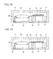
- Figs. 1A and 1B are schematic cross-sectional views showing a state in which an acoustic sensor disclosed in Fig. 7 and Fig. 8 of Japanese Unexamined Patent Publication No. 2008-301434 is mounted in a package.
- the acoustic sensor 11 has a diaphragm 14 (vibration thin film) laminated on a silicon substrate 12 with a back chamber 13 opened, and a back plate 15 arranged on the silicon substrate 12 to cover the diaphragm 14.
- Such an acoustic sensor 11 is normally mounted in a package 17 along with an IC circuit 16, as shown in Figs. 1A and 1B , where an electrode pad 18 of the acoustic sensor 11 and the IC circuit 16 are wire connected with a bonding wire 19, and the IC circuit 16 is wire connected to an electrode section 21 of the package 17 with a bonding wire 20.
- the bonding wire 19 is fixed by the resin 23 so that the bonding wire 19 does not bend and the foreign substance does not enter, but the acoustic sensor 11 which is the sound receiving unit cannot be sealed with resin as acoustic vibration will be shielded if sealed with resin.
- the surface of the silicon substrate is covered with an insulation coating (SiO 2 film), but the reliability is low for preventing short circuit since the insulation coating is thin.
- the back plate is extended up to the edge of the silicon substrate.
- this is a view in which the outer peripheral part of the silicon substrate where upper surface is exposed is omitted, as apparent from the cross-sectional view of Fig. 4 of Japanese Unexamined Patent Publication No. 2008-301434 , and the back plate is not actually extended up to the edge of the silicon substrate.
- Fig. 2 of Japanese Unexamined Patent Publication No. 2009-89097 discloses an acoustic sensor in which a structural object is arranged up to the outer peripheral edge of the upper surface of the silicon substrate to cover the upper surface of the silicon substrate.
- the outer peripheral part of the upper surface of the silicon substrate is covered with a member (surface layer protective film etc.) different from the back plate (plate including upper layer conductive film). The man hour in time of manufacturing thus increases, and the productivity is not satisfactory.
- the present invention has been devised to solve the problems described above, and an object thereof is to protect an outer peripheral part of an upper surface of a silicon substrate with a protective film using a back plate.
- an acoustic sensor including a semiconductor substrate including a back chamber, a conductive diaphragm arranged on an upper side of the semiconductor substrate, an insulating fixed film fixed to an upper surface of the semiconductor substrate so as to cover the diaphragm with a gap, a conductive fixed electrode film arranged on the fixed film at a position facing the diaphragm, and an electrode terminal for outputting change in electrostatic capacitance between the fixed electrode film and the diaphragm to outside as an electric signal, wherein an outer peripheral part of the upper surface of the semiconductor substrate is covered by a protective film made from a material identical to the fixed film, and an outer periphery of the protective film coinciding with an outer periphery of the upper surface of the semiconductor substrate.
- the thickness of the protective film can be increased and the insulation properties at the outer peripheral part of the upper surface of the semiconductor substrate can be enhanced since the outer peripheral part of the upper surface of the semiconductor substrate to the outer periphery (end edge) is covered with a protective film having insulation properties made from the same material as the fixed film. Therefore, the bonding wire connected to the electrode terminal is prevented from being bent and brought into contact with the upper surface of the semiconductor substrate and the foreign substance is prevented from being caught between the bonding wire and the upper surface of the semiconductor substrate and causing short circuit. Furthermore, since the protective film is made from the same material as the fixed film and the protective film can be formed in the same process as the fixed film, the man hour for manufacturing the acoustic sensor does not increase and the productivity does not lower from arranging the protective film.
- the protective film is fixed to the surface of the semiconductor substrate with an adhesive layer that is made from a material different from the fixed film and that is thinner than the protective film interposed.
- the adhesive layer of thin film thinner than the protective film is formed between the protective film and the semiconductor substrate to reduce the film stress generated at the protective film and alleviate the stripping of the protective film by the film stress.
- the protective film is a thin film, the throughput is less likely to lower even when forming a plurality of acoustic sensors on the wafer in the manufacturing process and then separating it into individual acoustic sensors by laser dicing at the area where the adhesive layer is formed.
- the outer peripheral part of the protective film is fixed to the surface of the semiconductor substrate with the adhesive layer interposed in between, and the inner peripheral part of the protective film is fixed to the surface of the semiconductor substrate with a thick film layer made from a material different from the fixed film interposed in between.
- the stripping of the protective film can be alleviated, and the throughput is less likely to lower even when individually separating the acoustic sensor formed on the wafer by laser dicing.
- the thick film portion is formed at the inner peripheral part and the height of the surface of the protective film is high, an electrode terminal can be arranged at the relevant portion.
- the thick film layer is preferably formed from a material same as the adhesive layer.
- the electrode terminal is arranged on the protective film in the region formed with the thick film layer. According to such an aspect, the distance between the electrode terminal and the upper surface of the semiconductor substrate can be increased, so that the parasitic capacitance between the electrode terminal and the semiconductor substrate can be reduced, the lowering in sensitivity of the acoustic sensor by the parasitic capacitance can be reduced and the acoustic characteristics can be enhanced.
- the adhesive layer and the thick film layer are formed from an insulating material. According to such an aspect, the insulation properties between the protective film and the semiconductor substrate can be enhanced.
- the protective film and the fixed film are continued, and a boundary region of the protective film and the fixed film is adhered to the upper surface of the semiconductor substrate.
- the adhesive layer and the thick film layer can be separated from the void portion even if the protective film and the fixed film are continued, thereby facilitating the manufacturing of the acoustic sensor.
- a manufacturing method of an acoustic sensor including a semiconductor substrate including a back chamber, a conductive diaphragm arranged on the upper side of the semiconductor substrate, an insulating fixed film fixed on an upper surface of the semiconductor substrate to cover the diaphragm with a gap, a conductive fixed electrode film arranged on the fixed film at a position facing the diaphragm, and an electrode terminal for outputting change in electrostatic capacitance between the fixed electrode film and the diaphragm to outside as an electric signal
- the manufacturing method including the steps of forming the diaphragm inside a sacrifice layer deposited on the upper surface of the semiconductor substrate, forming a space shaping portion in which a surface has an inner surface shape of the fixed film by etching the sacrifice layer, forming the fixed film on the shaped sacrifice layer and covering an outer peripheral part of the upper surface of the semiconductor substrate with a protective film made from a material same as the fixed film so that an outer periphery coincides with an
- the thickness of the protective film can be increased and the insulation properties at the outer peripheral part of the upper surface of the semiconductor substrate can be enhanced since the outer peripheral part of the upper surface of the semiconductor substrate to the outer periphery thereof (end edge) is covered with the protective film having insulation properties made from the same material as the fixed film. Therefore, the bonding wire connected to the electrode terminal is prevented from being bent and brought into contact with the upper surface of the semiconductor substrate and the foreign substance is prevented from being caught between the bonding wire and the upper surface of the semiconductor substrate, and causing short circuit. Furthermore, since the protective film is made from the same material as the fixed film and the protective film can be formed in the same process as the fixed film, the manufacturing man hour of the acoustic sensor does not increase and the productivity does not lower from arranging the protective film.
- an adhesive layer that is made from a material different from the fixed film and that is thinner than the protective film is formed in at least one part of the outer peripheral part of the upper surface of the semiconductor substrate after forming the space shaping portion.
- the thickness of the adhesive layer is preferably smaller than an interval between the inner surface of the back plate including the fixed film and the fixed electrode film, and the diaphragm.
- the adhesive layer of thin film thinner than the protective film is formed between the protective film and the semiconductor substrate to reduce the film stress generated at the protective film and alleviate the stripping of the protective film by the film stress.
- the adhesive layer is a thin film
- the throughput is less likely to lower when forming a plurality of acoustic sensors on a wafer in the manufacturing process and then separating into individual acoustic sensors by laser dicing at the area where the adhesive layer is formed.
- the adhesive film is arranged separate from the space shaping portion after forming the space shaping portion, and hence the adhesive film can be easily formed to a thin film.
- a thick film layer is formed on the outer side of the space shaping portion separate from the space shaping portion by the sacrifice layer and then the adhesive layer is formed on the outer side of the thick film layer when forming the space shaping portion.
- the thin film layer can be formed from the sacrifice layer at the same time as the space shaping portion, and hence the manufacturing process of the acoustic sensor can be simplified.
- the adhesive layer and the thick film layer are preferably formed with the same material.
- the adhesive layer and the thick film layer are formed from an insulating material. According to such an aspect, the insulation properties between the protective film and the semiconductor substrate can be enhanced.
- the thickness of the thick film layer is greater than an interval between the inner surface of the back plate including the fixed film and the fixed electrode film and the diaphragm.
- the thickness of the thick film layer is desirably equal to the distance of the sum of the interval between the inner surface of the back plate including the fixed film and the fixed electrode film and the diaphragm, and the interval between the upper surface of the semiconductor substrate and the diaphragm.
- the thick film layer can be formed using the sacrifice layer for forming the void portion in the fixed film, so that the manufacturing of the acoustic sensor can be facilitated.
- the protective film and the fixed film are continuously formed at the same time, and the boundary region of the protective film and the fixed film is adhered to the upper surface of the semiconductor substrate.
- the adhesive layer and the thick film layer can be separated from the void portion even if the protective film and the fixed film are continued, the adhesive layer and the thick film layer are prevented from being etched when etching the sacrifice layer to form the void portion, and the manufacturing of the acoustic sensor can be facilitated.
- the means for solving the problems of the invention has a characteristic of appropriately combining the configuring elements described above, and the present invention enables a great number of variations by the combination of the configuring elements.
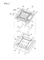
- Fig. 2 is a perspective view showing the acoustic sensor 31 in a partially exploded manner.
- Fig. 3 is a cross-sectional view in a diagonal direction showing the structure of the acoustic sensor 31.
- the acoustic sensor 31 is a microscopic capacitance type element manufactured using the MEMS technique, where a diaphragm 33 is arranged on an upper surface of a silicon substrate 32 (semiconductor substrate) through an anchor 37, and a back plate 34 is fixed thereon through a microscopic gap (void), as shown in Fig. 3 .
- the silicon substrate 32 is made of a monocrystal silicon. As shown in Fig. 2 , the silicon substrate 32 is formed to a rectangular shape, and includes a back chamber 35 having a square hole shape that passes from the front surface to the back surface. The inner peripheral surface of the back chamber 35 may be a perpendicular surface or may be inclined to a tapered form. The opening at the lower surface of the back chamber 35 is blocked by a package when the acoustic sensor 31 is mounted in the package (see Figs. 1A and 1B ).
- each of the anchors 37 is positioned within a recessed area formed to cut the inner peripheral edge of the base part 41 in the diagonal direction of the back chamber 35.
- the region on the outer side than the base part 41 of the upper surface of the silicon substrate 32 is covered by an adhesive layer 47 thinner than the base part 41, where the outer periphery (end edge) of the adhesive layer matches the end edge of the silicon substrate 32.
- the anchor 37 and the base part 41 are made from SiO 2 .
- the adhesive layer 47 is made from SiO 2 or polysilicon.
- the diaphragm 33 is formed by a polysilicon thin film having a small film thickness, and has conductivity.
- the diaphragm 33 has the beam portions 36a extended outward in the diagonal direction from four corners of a rectangular vibration thin film 36b.
- An extraction wiring 43 is extended from one of the beam portions 36a.
- the diaphragm 33 is arranged on the upper surface of the silicon substrate 32 so that the vibration thin film 36b covers the upper surface of the back chamber 35.
- Each of the beam portions 36a of the diaphragm 33 is positioned in the recessed area of the base part 41, and the lower surface of the distal end of each beam portion 36a is fixed to the anchor 37. Therefore, the vibration thin film 36b of the diaphragm 33 floats in the air at the upper side of the back chamber 35, and film vibrates in response to the acoustic vibration (air vibration).
- the back plate 34 is formed by arranging a fixed electrode film 40 made of polysilicon on the lower surface of a plate portion 39 (fixed film) made of nitride film (SiN).
- the back plate 34 has a canopy shape and includes a hollow portion underneath, and covers the diaphragm 33.
- the height a (height from the upper surface of the silicon substrate 32 to the lower surface of the fixed electrode film 40) of the hollow portion under the back plate 34 is equal to the thickness c of the base part 41 formed at the upper surface of the silicon substrate 32.
- a microscopic void is formed between the lower surface of the back plate 34 (i.e., lower surface of fixed electrode film 40) and the upper surface of the diaphragm 33.
- a beam portion cover region 49 arranged at the corner of the back plate 34 covers the beam portion 36a through the microscopic void.
- the fixed electrode film 40 faces the vibration thin film 36b which is the movable electrode film and configures a capacitor.
- the back plate 34 has a great number of acoustic holes 38 for passing the acoustic vibration perforated so as to pass from the upper surface to the lower surface.
- a small gap (passage of acoustic vibration) is also formed between the lower surface at the outer peripheral part of the vibration thin film 36b and the upper surface of the silicon substrate 32. Therefore, the acoustic vibration that entered the back plate 34 through the acoustic holes 38 vibrates the vibration thin film 36b, and also exits to the back chamber 35 through the gap between the outer peripheral part of the vibration thin film 36b and the silicon substrate 32.
- a great number of microscopic stoppers 42 are projected out at the inner surface of the back plate 34 to prevent the diaphragm 33 from being adsorbed or attached (stuck) to the lower surface of the back plate 34 and not returning,
- a protective film 53 is continuously extended over the entire periphery from the outer peripheral edge of the canopy shaped plate portion 39. Therefore, the protective film 53 is made from a nitride film (SiN) same as the plate potion 39, and has substantially the same film thickness as the plate portion 39.
- the inner peripheral part of the protective film 53 is a base covering part 51 having a reverse groove shaped cross-section, where the outer peripheral part of the protective film 53 is a flat part 52.
- a boundary region 50 between the outer periphery of the back plate 34 and the inner periphery of the protective film 53 has a V groove shaped cross-section.
- the back plate 34 is fixed to the upper surface of the silicon substrate 32, and the protective film 53 covers the outer peripheral part of the upper surface of the silicon substrate 32 with the base part 41 and the adhesive layer 47 interposed in between.
- the base covering part 51 of the protective film 53 covers the base part 41 and the flat part 52 covers the upper surface of the adhesive layer 47, where the outer periphery (end edge) of the flat part 52 coincides with the outer periphery of the adhesive layer 47 and the outer periphery of the upper surface of the silicon substrate 32.
- the lower surface of the boundary region 50 between the back plate 34 and the protective film 53 is adhered to the exposed surface 48 of the inner periphery of the base part 41, where the hollow portion under the back plate 34 and the base part 41 are separated by the boundary region 50.
- the thickness b of the void (air gap) between the upper surface of the diaphragm 33 and the lower surface of the back plate 34 is about 2 ⁇ m.
- the thickness c of the base part 41 is greater than the thickness b of the void between the anchor 37 and the back plate 34 and is greater than or equal to 2 ⁇ m.
- the thickness d of the adhesive layer 47 is smaller than the thickness b of the void between the anchor 37 and the back plate 34, and is smaller than or equal to 2 ⁇ m.
- the width e of the protective film 53 is preferably smaller than or equal to 400 ⁇ m, and the width f of the flat part 52 is preferably about 150 ⁇ m.
- An opening is formed in the base covering part 51, where a movable side electrode pad 46 (electrode terminal) is formed on the upper surface of the extraction wiring 43 through the relevant opening, and such a movable side electrode pad 46 is conducted to the extraction wiring 43 (therefore to the diaphragm 33).
- a fixed side electrode pad 45 (electrode terminal) arranged on the upper surface of the plate portion 39 is conducted to the extraction wiring 44 (therefore to the fixed electrode film 40) through a through-hole and the like.
- the diaphragm 33 which is a thin film, is excited by the acoustic vibration and film vibrates when the acoustic vibration passes through the acoustic hole 38 and enters the space between the back plate 34 and the diaphragm 33.
- the diaphragm 33 vibrates and the gap distance between the diaphragm 33 and the fixed electrode film 40 changes, the electrostatic capacitance between the diaphragm 33 and the fixed electrode film 40 changes.
- the acoustic vibration (change in sound pressure) sensed by the diaphragm 33 becomes the change in electrostatic capacitance between the diaphragm 33 and the fixed electrode film 40, and is outputted as an electrical signal.
- the outer peripheral part of the upper surface of the silicon substrate 32 (region to cut from the wafer and sometimes referred to as a dicing street part) is covered by the flat part 52 of the protective film 53.
- the protective film 53 is formed by an SiN film and is formed to a relatively thick film thickness, and thus excels in insulation properties. Therefore, the bonding wire merely touches the protective film 53 and does not directly touch the silicon substrate 32 even if the bonding wire connected to the fixed side electrode pad 45 and the movable side electrode pad 46 is bent and sagged downward. Furthermore, even if a foreign substance gets caught under the bonding wire, such a foreign substance is shielded by the protective film 53 and thus does not directly touch the silicon substrate 32. The short circuit of the acoustic sensor 31 thus can be effectively prevented.
- the adhesive layer 47 is made from a thin SiO 2 or a polysilicon thinner than the thickness b of the void, and the flat part 52 is formed on the upper surface of the silicon substrate 32 through the adhesive layer 47, and hence the film stress generated at the protective film 53 can be reduced and the stripping of the protective film 53 due to the film stress can be alleviated.
- the adhesiveness of the flat part 52 can be enhanced by interposing the adhesive layer 47 made of SiO 2 or SiN.
- the base part 41 is made of SiO 2 thicker than the thickness b of the void, and the fixed side electrode pad 45 is arranged on the protective film 53 (base covering part 51) at the upper side of the base part 41, so that the distance between the fixed side electrode pad 45 and the upper surface of the silicon substrate 32 can be increased.
- the parasitic capacitance between the electrode pads 45, 46 and the silicon substrate 32 can be reduced, whereby the lowering in sensitivity of the acoustic sensor 31 by the parasitic capacitance can be reduced, and the acoustic characteristics of the acoustic sensor 31 can be enhanced.
- the adhesiveness of the base covering part 51 can be enhanced since the base covering part 51 is formed on the base part 41 made of SiO 2 .
- the effect of reducing the parasitic capacitance cannot be obtained by thickening the base part 41 since the movable side electrode pad 46 is formed at the end of the beam portion 36a of the diaphragm 33.
- the effect of reducing the parasitic capacitance by thickening the base part 41 can be obtained by adopting a structure similar to the fixed side electrode pad 45 for the movable side electrode pad 46, that is, by arranging the extraction wiring on the upper surface of the plate portion 39 through the through-hole and the like to achieve conduction.
- the acoustic sensor 31 has the outermost surface covered with the SiN layer (i.e., plate portion 39 and protective film 53) having high moisture absorption resistance.
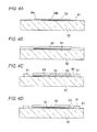
- Figs. 4A to 4D and Figs. 5A to 5C are schematic cross-sectional views showing the manufacturing process of the acoustic sensor 31.
- a sacrifice layer 61 made of silicon oxide film (SiO 2 ) is formed on the surface of the monocrystal silicon substrate 32 through thermal oxidation, CVD method, and the like.
- a polysilicon layer is then formed on the sacrifice layer 61, which polysilicon layer is patterned by etching to form a flat diaphragm 33 in which the beam portions 36a are extended from four corners of the vibration thin film 36b.
- a sacrifice layer 61 is further deposited on the sacrifice layer 61 from above the diaphragm 33 to cover the diaphragm 33 with the sacrifice layer 61, so that the diaphragm 33 is embedded in the sacrifice layer 61 as shown in Fig. 4B ,
- the sacrifice layer 61 is etched to form a void shaped portion 62 having the inner surface shape of the back plate 34 and the base part 41 from the sacrifice layer 6.1.
- the void shaped part 62 and the base part 41 are separated by a groove 63, and the upper surface of the silicon substrate 32 is exposed in the groove 63 (bottom surface of the groove 63 becomes the exposed surface 48) and the upper surface of the silicon substrate 32 is exposed even on the outer side of the base part 41.
- a hole 64 for forming the stopper 42 is dug at the upper surface of the void shaped part 62.
- the thin adhesive layer 47 is formed by SiO 2 or polysilicon so as to continue to the outer peripheral surface of the base part 41 at the upper surface of the silicon substrate 32 on the outer side of the base part 41,
- a polysilicon film is formed on the upper surface of the void shaped part 62, and the polysilicon film is patterned by etching to form the fixed electrode film 40.
- the acoustic hole 38 is opened in the fixed electrode film 40 and the through hole is opened in accordance with the hole 64.
- an SiN layer having a hydrofluoric acid resistance property is deposited from above the fixed electrode film 40 to form the plate portion 39.
- the stopper 42 for preventing fixed attachment is formed by the SiN layer deposited in the hole 64.
- the acoustic hole 38 is also formed in the plate portion 39 in alignment with the acoustic hole 38 of the fixed electrode film 40, and the acoustic hole 38 is also passed through the back plate 34. Furthermore, the electrode pads 45, 46 are arranged on the base covering part 51.
- the central part of the silicon substrate 32 is etched from the lower surface side, and the back chamber 35 is passed through the silicon substrate 32 as shown in Fig. 5B to expose the void shaped part 62 at the upper surface of the back chamber 35.
- the hydrofluoric acid is introduced from the acoustic hole 38 of the back plate 34, the back chamber 35 of the silicon substrate 32, and the like to selectively wet etch the void shaped part 62, and the void shaped part 62 is removed leaving only the sacrifice layer 61 under the beam portion 36a as the anchor 37 as shown in Fig. 5C .
- the diaphragm 33 floats from the upper surface of the silicon substrate 32 by the anchor 37, and supported so as to vibrate on the back chamber 35, whereby an air gap forms between the fixed electrode film 40 and the diaphragm 33, Since the base part 41 and the void shaped part 62 are partitioned by the boundary region 50, the base part 41 is not etched with the hydrofluoric acid and the base part 41 and the adhesive layer 47 remain as is.
- the acoustic sensor 31 is formed in such a manner.
- the thickness of the base part 41 is made larger than the thickness b of the void between the upper surface of the diaphragm 33 and the lower surface of the back plate 34 in the acoustic sensor 31 for the hollowing reasons in terms of method.
- the productivity becomes the most satisfactory if the base part 41 is formed from the same sacrifice layer 61 through the process same as the void shaped part 62 as in the manufacturing method described.
- the thickness c of the base part 41 needs to be thicker than the thickness b of the void (c ⁇ b).
- the void between the diaphragm 33 and the back plate 34 is narrowed, such a void is preferably as wide as possible to prevent the pull in phenomenon (phenomenon in which the diaphragm 33 and the fixed electrode film 40 attach due to electrostatic attractive force at the time of voltage application) the stick phenomenon (phenomenon in which the diaphragm 33 and the fixed electrode film 40 attach due to moisture etc. that entered the void) and the like.
- the void is also desirably as wide as possible to reduce the heat noise that becomes the noise source.
- the void between the diaphragm 33 and the back plate 34 thus cannot be made thinner than or equal to 2 ⁇ m, and the thickness b of the void is generally greater than or equal to 2 ⁇ m.
- the base part 41 is desirably as thick as possible to reduce the parasitic capacitance between the fixed side electrode pad 45 and the silicon substrate 32.
- the base part 41 can ensure a constant thickness or more (i.e., thickness of greater than or equal to 2 ⁇ m) by having the thickness C of the base part 41 greater than the thickness b of the void, and hence the parasitic capacitance can obviously be reduced,
- the thickness c of the base part 41 is the same as the total of the thickness b of the void and the thickness g of the anchor 37.
- the productivity is the most preferable if the process of forming the base part 41 and the process of forming the void or anchor thickness are synchronized, whereby the thickness c of the base part 41 becomes equal to the total of the thickness c of the void and the thickness g of the anchor 37.
- the thickness of the adhesive layer 47 is formed smaller than the thickness b of the void between the upper surface of the diaphragm 33 and the lower surface of the back plate 34 for the following reasons in terms of method.
- the adhesive layer 47 arranged on the dicing street part desirably has a thin thickness when using laser dicing. However, the thickness of the adhesive layer 47 becomes thick when simultaneously forming the adhesive layer 47 using the sacrifice layer 61 for forming the void shaped part 62 and the base part 41. Therefore, the adhesive layer 47 is desirably formed in a process different from the base part 41 and the void shaped part 62, as shown in Fig. 4D .
- the thickness d of the adhesive layer 47 formed in the process of Fig. 4D is preferably as thin as possible, and hence is desirably formed from an SiO 2 film having a thickness of about 0.1 ⁇ m.
- the adhesive layer 47 is formed in the process after the void shaped part 62 and the base part 41 are formed, so that the film same as the adhesive layer 47 is sometimes applied to the surface of the void shaped part 62 and the base part 41 depending on the method of forming the adhesive layer 47.
- the thickness of the void shaped part 62 and the base part 41 increases by the thickness of the adhesive layer 47.
- the thickness of the sacrifice layer 61 formed in the process of Fig. 4B is made thinner than the target thickness of the void shaped part 62 and the base part 41 by the thickness of the adhesive layer 47.
Landscapes
- Engineering & Computer Science (AREA)
- Physics & Mathematics (AREA)
- Acoustics & Sound (AREA)
- Signal Processing (AREA)
- Health & Medical Sciences (AREA)
- General Health & Medical Sciences (AREA)
- Toxicology (AREA)
- Computer Hardware Design (AREA)
- Microelectronics & Electronic Packaging (AREA)
- Manufacturing & Machinery (AREA)
- Pressure Sensors (AREA)
- Electrostatic, Electromagnetic, Magneto- Strictive, And Variable-Resistance Transducers (AREA)
Abstract
Description
- The present invention relates to acoustic sensors and methods for manufacturing the same, and specifically to a MEMS (Micro Electro Mechanical Systems) type acoustic sensor manufactured using a MEMS technique, and a method for manufacturing the same.
- The MEMS acoustic sensor is disclosed in Japanese Unexamined Patent Publication Nos.
2008-301434 2009-89097 -
Figs. 1A and 1B are schematic cross-sectional views showing a state in which an acoustic sensor disclosed in Fig. 7 and Fig. 8 of Japanese Unexamined Patent Publication No.2008-301434 acoustic sensor 11 has a diaphragm 14 (vibration thin film) laminated on asilicon substrate 12 with aback chamber 13 opened, and aback plate 15 arranged on thesilicon substrate 12 to cover thediaphragm 14. Such anacoustic sensor 11 is normally mounted in apackage 17 along with anIC circuit 16, as shown inFigs. 1A and 1B , where anelectrode pad 18 of theacoustic sensor 11 and theIC circuit 16 are wire connected with abonding wire 19, and theIC circuit 16 is wire connected to anelectrode section 21 of thepackage 17 with abonding wire 20. - In such an
acoustic sensor 11, however, the outer peripheral part at the upper surface of thesilicon substrate 12 is completely exposed. Therefore, as shown inFig. 1A , if thebonding wire 19 connecting theacoustic sensor 11 and theIC circuit 16 bends downward due to some kind of load, thebonding wire 19 may come into contact with thesilicon substrate 12, thereby causing short circuit in theacoustic sensor 11. Even if thebonding wire 19 is not bent, if a foreign substance 22 (e.g., microscopic dust etc.) gets caught between thebonding wire 19 and the upper surface of thesilicon substrate 12 as shown inFig. 1B , short circuit may occur between theelectrode pad 18 and thesilicon substrate 12 through theforeign substance 22. - Since the
IC circuit 16 is entirely sealed with aresin 23, thebonding wire 19 is fixed by theresin 23 so that thebonding wire 19 does not bend and the foreign substance does not enter, but theacoustic sensor 11 which is the sound receiving unit cannot be sealed with resin as acoustic vibration will be shielded if sealed with resin. - In the acoustic sensor disclosed in
Fig. 4 andFig. 5 of Japanese Unexamined Patent Publication No.2008-301434 2008-301434 Fig. 4 of Japanese Unexamined Patent Publication No.2008-301434 -
Fig. 2 of Japanese Unexamined Patent Publication No.2009-89097 - The present invention has been devised to solve the problems described above, and an object thereof is to protect an outer peripheral part of an upper surface of a silicon substrate with a protective film using a back plate.
- In accordance with one aspect of the present invention, there is provided an acoustic sensor including a semiconductor substrate including a back chamber, a conductive diaphragm arranged on an upper side of the semiconductor substrate, an insulating fixed film fixed to an upper surface of the semiconductor substrate so as to cover the diaphragm with a gap, a conductive fixed electrode film arranged on the fixed film at a position facing the diaphragm, and an electrode terminal for outputting change in electrostatic capacitance between the fixed electrode film and the diaphragm to outside as an electric signal, wherein an outer peripheral part of the upper surface of the semiconductor substrate is covered by a protective film made from a material identical to the fixed film, and an outer periphery of the protective film coinciding with an outer periphery of the upper surface of the semiconductor substrate.
- In the acoustic sensor of the present invention, the thickness of the protective film can be increased and the insulation properties at the outer peripheral part of the upper surface of the semiconductor substrate can be enhanced since the outer peripheral part of the upper surface of the semiconductor substrate to the outer periphery (end edge) is covered with a protective film having insulation properties made from the same material as the fixed film. Therefore, the bonding wire connected to the electrode terminal is prevented from being bent and brought into contact with the upper surface of the semiconductor substrate and the foreign substance is prevented from being caught between the bonding wire and the upper surface of the semiconductor substrate and causing short circuit. Furthermore, since the protective film is made from the same material as the fixed film and the protective film can be formed in the same process as the fixed film, the man hour for manufacturing the acoustic sensor does not increase and the productivity does not lower from arranging the protective film.
- In one aspect of the acoustic sensor according to the present invention, at least one part of the protective film is fixed to the surface of the semiconductor substrate with an adhesive layer that is made from a material different from the fixed film and that is thinner than the protective film interposed. According to such an aspect, the adhesive layer of thin film thinner than the protective film is formed between the protective film and the semiconductor substrate to reduce the film stress generated at the protective film and alleviate the stripping of the protective film by the film stress. Furthermore, since the protective film is a thin film, the throughput is less likely to lower even when forming a plurality of acoustic sensors on the wafer in the manufacturing process and then separating it into individual acoustic sensors by laser dicing at the area where the adhesive layer is formed.
- In another aspect of the acoustic sensor according to the present invention, the outer peripheral part of the protective film is fixed to the surface of the semiconductor substrate with the adhesive layer interposed in between, and the inner peripheral part of the protective film is fixed to the surface of the semiconductor substrate with a thick film layer made from a material different from the fixed film interposed in between. According to such an aspect, the stripping of the protective film can be alleviated, and the throughput is less likely to lower even when individually separating the acoustic sensor formed on the wafer by laser dicing. Furthermore, since the thick film portion is formed at the inner peripheral part and the height of the surface of the protective film is high, an electrode terminal can be arranged at the relevant portion. The thick film layer is preferably formed from a material same as the adhesive layer.
- In still another aspect of the acoustic sensor according to the present invention, the electrode terminal is arranged on the protective film in the region formed with the thick film layer. According to such an aspect, the distance between the electrode terminal and the upper surface of the semiconductor substrate can be increased, so that the parasitic capacitance between the electrode terminal and the semiconductor substrate can be reduced, the lowering in sensitivity of the acoustic sensor by the parasitic capacitance can be reduced and the acoustic characteristics can be enhanced.
- In yet another aspect of the acoustic sensor according to the present invention, the adhesive layer and the thick film layer are formed from an insulating material. According to such an aspect, the insulation properties between the protective film and the semiconductor substrate can be enhanced.
- In yet another aspect of the acoustic sensor according to the present invention, the protective film and the fixed film are continued, and a boundary region of the protective film and the fixed film is adhered to the upper surface of the semiconductor substrate. According to such an aspect, the adhesive layer and the thick film layer can be separated from the void portion even if the protective film and the fixed film are continued, thereby facilitating the manufacturing of the acoustic sensor.
- In accordance with another aspect of the present invention, there is provided a manufacturing method of an acoustic sensor including a semiconductor substrate including a back chamber, a conductive diaphragm arranged on the upper side of the semiconductor substrate, an insulating fixed film fixed on an upper surface of the semiconductor substrate to cover the diaphragm with a gap, a conductive fixed electrode film arranged on the fixed film at a position facing the diaphragm, and an electrode terminal for outputting change in electrostatic capacitance between the fixed electrode film and the diaphragm to outside as an electric signal, the manufacturing method including the steps of forming the diaphragm inside a sacrifice layer deposited on the upper surface of the semiconductor substrate, forming a space shaping portion in which a surface has an inner surface shape of the fixed film by etching the sacrifice layer, forming the fixed film on the shaped sacrifice layer and covering an outer peripheral part of the upper surface of the semiconductor substrate with a protective film made from a material same as the fixed film so that an outer periphery coincides with an outer periphery of the upper surface of the semiconductor substrate, forming the back chamber in the semiconductor substrate, and supporting the diaphragm in space by removing the sacrifice layer by etching and forming a gap between the diaphragm and the inner surface of the fixed film.
- In the manufacturing method of the acoustic sensor according to the present invention, the thickness of the protective film can be increased and the insulation properties at the outer peripheral part of the upper surface of the semiconductor substrate can be enhanced since the outer peripheral part of the upper surface of the semiconductor substrate to the outer periphery thereof (end edge) is covered with the protective film having insulation properties made from the same material as the fixed film. Therefore, the bonding wire connected to the electrode terminal is prevented from being bent and brought into contact with the upper surface of the semiconductor substrate and the foreign substance is prevented from being caught between the bonding wire and the upper surface of the semiconductor substrate, and causing short circuit. Furthermore, since the protective film is made from the same material as the fixed film and the protective film can be formed in the same process as the fixed film, the manufacturing man hour of the acoustic sensor does not increase and the productivity does not lower from arranging the protective film.
- In an aspect of the manufacturing method of the acoustic sensor according to the present invention, an adhesive layer that is made from a material different from the fixed film and that is thinner than the protective film is formed in at least one part of the outer peripheral part of the upper surface of the semiconductor substrate after forming the space shaping portion. In particular, the thickness of the adhesive layer is preferably smaller than an interval between the inner surface of the back plate including the fixed film and the fixed electrode film, and the diaphragm. According to such an aspect, the adhesive layer of thin film thinner than the protective film is formed between the protective film and the semiconductor substrate to reduce the film stress generated at the protective film and alleviate the stripping of the protective film by the film stress. Furthermore, since the adhesive layer is a thin film, the throughput is less likely to lower when forming a plurality of acoustic sensors on a wafer in the manufacturing process and then separating into individual acoustic sensors by laser dicing at the area where the adhesive layer is formed. The adhesive film is arranged separate from the space shaping portion after forming the space shaping portion, and hence the adhesive film can be easily formed to a thin film.
- In another aspect of the manufacturing method of the acoustic sensor according to the present invention, a thick film layer is formed on the outer side of the space shaping portion separate from the space shaping portion by the sacrifice layer and then the adhesive layer is formed on the outer side of the thick film layer when forming the space shaping portion. According to such an aspect, the thin film layer can be formed from the sacrifice layer at the same time as the space shaping portion, and hence the manufacturing process of the acoustic sensor can be simplified. The adhesive layer and the thick film layer are preferably formed with the same material.
- In another further aspect of the manufacturing method of the acoustic sensor according to the present invention, the adhesive layer and the thick film layer are formed from an insulating material. According to such an aspect, the insulation properties between the protective film and the semiconductor substrate can be enhanced.
- In another further aspect of the acoustic sensor according to the present invention, the thickness of the thick film layer is greater than an interval between the inner surface of the back plate including the fixed film and the fixed electrode film and the diaphragm. In particular, the thickness of the thick film layer is desirably equal to the distance of the sum of the interval between the inner surface of the back plate including the fixed film and the fixed electrode film and the diaphragm, and the interval between the upper surface of the semiconductor substrate and the diaphragm. According to such an aspect, the thick film layer can be formed using the sacrifice layer for forming the void portion in the fixed film, so that the manufacturing of the acoustic sensor can be facilitated.
- In still another aspect of the manufacturing method of the acoustic sensor according to the present invention, the protective film and the fixed film are continuously formed at the same time, and the boundary region of the protective film and the fixed film is adhered to the upper surface of the semiconductor substrate. According to such an aspect, the adhesive layer and the thick film layer can be separated from the void portion even if the protective film and the fixed film are continued, the adhesive layer and the thick film layer are prevented from being etched when etching the sacrifice layer to form the void portion, and the manufacturing of the acoustic sensor can be facilitated.
- The means for solving the problems of the invention has a characteristic of appropriately combining the configuring elements described above, and the present invention enables a great number of variations by the combination of the configuring elements.
-
-
Figs. 1A and 1B are cross-sectional views showing a state in which an acoustic sensor disclosed in Japanese Unexamined Patent Publication No.2008-301434 -
Fig. 2 is an exploded perspective view of an acoustic sensor according to a first embodiment of the present invention; -
Fig. 3 is a cross-sectional view of the acoustic sensor of the first embodiment; -
Figs. 4A to 4D are schematic cross-sectional views describing the manufacturing process of the acoustic sensor of the first embodiment; and -
Figs, 5A to 5C are schematic cross-sectional views describing the manufacturing process of the acoustic sensor of the first embodiment, showing the process followingFig. 4D . - Hereinafter, preferred embodiments of the present invention will be described with reference to the accompanying drawings. It should be recognized that the present invention is not limited to the following embodiments, and various design changes can be made within a scope not deviating from the gist of the present invention.
- First, a structure of an
acoustic sensor 31 according to a first embodiment of the present invention will be described with reference toFig. 2 andFig. 3 .Fig. 2 is a perspective view showing theacoustic sensor 31 in a partially exploded manner.Fig. 3 is a cross-sectional view in a diagonal direction showing the structure of theacoustic sensor 31. - The
acoustic sensor 31 is a microscopic capacitance type element manufactured using the MEMS technique, where adiaphragm 33 is arranged on an upper surface of a silicon substrate 32 (semiconductor substrate) through ananchor 37, and aback plate 34 is fixed thereon through a microscopic gap (void), as shown inFig. 3 . - The
silicon substrate 32 is made of a monocrystal silicon. As shown inFig. 2 , thesilicon substrate 32 is formed to a rectangular shape, and includes aback chamber 35 having a square hole shape that passes from the front surface to the back surface. The inner peripheral surface of theback chamber 35 may be a perpendicular surface or may be inclined to a tapered form. The opening at the lower surface of theback chamber 35 is blocked by a package when theacoustic sensor 31 is mounted in the package (seeFigs. 1A and 1B ). - Four anchors 37 for supporting the
beam portions 36a of thediaphragm 33 from the lower surface are arranged on the upper surface of thesilicon substrate 32, and a base part 41 (thick film layer) is formed to surround theback chamber 35 and theanchors 37. In particular, each of theanchors 37 is positioned within a recessed area formed to cut the inner peripheral edge of thebase part 41 in the diagonal direction of theback chamber 35. The region on the outer side than thebase part 41 of the upper surface of thesilicon substrate 32 is covered by anadhesive layer 47 thinner than thebase part 41, where the outer periphery (end edge) of the adhesive layer matches the end edge of thesilicon substrate 32. Theanchor 37 and thebase part 41 are made from SiO2. Theadhesive layer 47 is made from SiO2 or polysilicon. - The
diaphragm 33 is formed by a polysilicon thin film having a small film thickness, and has conductivity. Thediaphragm 33 has thebeam portions 36a extended outward in the diagonal direction from four corners of a rectangular vibrationthin film 36b. Anextraction wiring 43 is extended from one of thebeam portions 36a. - As shown in
Fig. 3 , thediaphragm 33 is arranged on the upper surface of thesilicon substrate 32 so that the vibrationthin film 36b covers the upper surface of theback chamber 35. Each of thebeam portions 36a of thediaphragm 33 is positioned in the recessed area of thebase part 41, and the lower surface of the distal end of eachbeam portion 36a is fixed to theanchor 37. Therefore, the vibrationthin film 36b of thediaphragm 33 floats in the air at the upper side of theback chamber 35, and film vibrates in response to the acoustic vibration (air vibration). - The
back plate 34 is formed by arranging a fixedelectrode film 40 made of polysilicon on the lower surface of a plate portion 39 (fixed film) made of nitride film (SiN). Theback plate 34 has a canopy shape and includes a hollow portion underneath, and covers thediaphragm 33. The height a (height from the upper surface of thesilicon substrate 32 to the lower surface of the fixed electrode film 40) of the hollow portion under theback plate 34 is equal to the thickness c of thebase part 41 formed at the upper surface of thesilicon substrate 32. A microscopic void is formed between the lower surface of the back plate 34 (i.e., lower surface of fixed electrode film 40) and the upper surface of thediaphragm 33. A beamportion cover region 49 arranged at the corner of theback plate 34 covers thebeam portion 36a through the microscopic void. The fixedelectrode film 40 faces the vibrationthin film 36b which is the movable electrode film and configures a capacitor. - The
back plate 34 has a great number ofacoustic holes 38 for passing the acoustic vibration perforated so as to pass from the upper surface to the lower surface. A small gap (passage of acoustic vibration) is also formed between the lower surface at the outer peripheral part of the vibrationthin film 36b and the upper surface of thesilicon substrate 32. Therefore, the acoustic vibration that entered theback plate 34 through theacoustic holes 38 vibrates the vibrationthin film 36b, and also exits to theback chamber 35 through the gap between the outer peripheral part of the vibrationthin film 36b and thesilicon substrate 32. - A great number of
microscopic stoppers 42 are projected out at the inner surface of theback plate 34 to prevent thediaphragm 33 from being adsorbed or attached (stuck) to the lower surface of theback plate 34 and not returning, - A
protective film 53 is continuously extended over the entire periphery from the outer peripheral edge of the canopy shapedplate portion 39. Therefore, theprotective film 53 is made from a nitride film (SiN) same as theplate potion 39, and has substantially the same film thickness as theplate portion 39. The inner peripheral part of theprotective film 53 is abase covering part 51 having a reverse groove shaped cross-section, where the outer peripheral part of theprotective film 53 is aflat part 52. Aboundary region 50 between the outer periphery of theback plate 34 and the inner periphery of theprotective film 53 has a V groove shaped cross-section. - The
back plate 34 is fixed to the upper surface of thesilicon substrate 32, and theprotective film 53 covers the outer peripheral part of the upper surface of thesilicon substrate 32 with thebase part 41 and theadhesive layer 47 interposed in between. Thebase covering part 51 of theprotective film 53 covers thebase part 41 and theflat part 52 covers the upper surface of theadhesive layer 47, where the outer periphery (end edge) of theflat part 52 coincides with the outer periphery of theadhesive layer 47 and the outer periphery of the upper surface of thesilicon substrate 32. The lower surface of theboundary region 50 between theback plate 34 and theprotective film 53 is adhered to the exposedsurface 48 of the inner periphery of thebase part 41, where the hollow portion under theback plate 34 and thebase part 41 are separated by theboundary region 50. - The thickness b of the void (air gap) between the upper surface of the
diaphragm 33 and the lower surface of theback plate 34 is about 2 µm. The thickness c of thebase part 41 is greater than the thickness b of the void between theanchor 37 and theback plate 34 and is greater than or equal to 2 µm. The thickness d of theadhesive layer 47 is smaller than the thickness b of the void between theanchor 37 and theback plate 34, and is smaller than or equal to 2 µm. The width e of theprotective film 53 is preferably smaller than or equal to 400 µm, and the width f of theflat part 52 is preferably about 150 µm. - An opening is formed in the
base covering part 51, where a movable side electrode pad 46 (electrode terminal) is formed on the upper surface of theextraction wiring 43 through the relevant opening, and such a movableside electrode pad 46 is conducted to the extraction wiring 43 (therefore to the diaphragm 33). A fixed side electrode pad 45 (electrode terminal) arranged on the upper surface of theplate portion 39 is conducted to the extraction wiring 44 (therefore to the fixed electrode film 40) through a through-hole and the like. - In such an
acoustic sensor 31, thediaphragm 33, which is a thin film, is excited by the acoustic vibration and film vibrates when the acoustic vibration passes through theacoustic hole 38 and enters the space between theback plate 34 and thediaphragm 33. When thediaphragm 33 vibrates and the gap distance between thediaphragm 33 and the fixedelectrode film 40 changes, the electrostatic capacitance between thediaphragm 33 and the fixedelectrode film 40 changes. As a result, in such anacoustic sensor 31, the acoustic vibration (change in sound pressure) sensed by thediaphragm 33 becomes the change in electrostatic capacitance between thediaphragm 33 and the fixedelectrode film 40, and is outputted as an electrical signal. - According to such an
acoustic sensor 31, the outer peripheral part of the upper surface of the silicon substrate 32 (region to cut from the wafer and sometimes referred to as a dicing street part) is covered by theflat part 52 of theprotective film 53. Similar to theplate portion 39, theprotective film 53 is formed by an SiN film and is formed to a relatively thick film thickness, and thus excels in insulation properties. Therefore, the bonding wire merely touches theprotective film 53 and does not directly touch thesilicon substrate 32 even if the bonding wire connected to the fixedside electrode pad 45 and the movableside electrode pad 46 is bent and sagged downward. Furthermore, even if a foreign substance gets caught under the bonding wire, such a foreign substance is shielded by theprotective film 53 and thus does not directly touch thesilicon substrate 32. The short circuit of theacoustic sensor 31 thus can be effectively prevented. - The
adhesive layer 47 is made from a thin SiO2 or a polysilicon thinner than the thickness b of the void, and theflat part 52 is formed on the upper surface of thesilicon substrate 32 through theadhesive layer 47, and hence the film stress generated at theprotective film 53 can be reduced and the stripping of theprotective film 53 due to the film stress can be alleviated. The adhesiveness of theflat part 52 can be enhanced by interposing theadhesive layer 47 made of SiO2 or SiN. - The
base part 41 is made of SiO2 thicker than the thickness b of the void, and the fixedside electrode pad 45 is arranged on the protective film 53 (base covering part 51) at the upper side of thebase part 41, so that the distance between the fixedside electrode pad 45 and the upper surface of thesilicon substrate 32 can be increased. As a result, the parasitic capacitance between theelectrode pads silicon substrate 32 can be reduced, whereby the lowering in sensitivity of theacoustic sensor 31 by the parasitic capacitance can be reduced, and the acoustic characteristics of theacoustic sensor 31 can be enhanced. Furthermore, the adhesiveness of thebase covering part 51 can be enhanced since thebase covering part 51 is formed on thebase part 41 made of SiO2. - In the example of
Fig. 2 , the effect of reducing the parasitic capacitance cannot be obtained by thickening thebase part 41 since the movableside electrode pad 46 is formed at the end of thebeam portion 36a of thediaphragm 33. However, the effect of reducing the parasitic capacitance by thickening thebase part 41 can be obtained by adopting a structure similar to the fixedside electrode pad 45 for the movableside electrode pad 46, that is, by arranging the extraction wiring on the upper surface of theplate portion 39 through the through-hole and the like to achieve conduction. - Furthermore, satisfactory moisture absorption resistance is obtained since the
acoustic sensor 31 has the outermost surface covered with the SiN layer (i.e.,plate portion 39 and protective film 53) having high moisture absorption resistance. - The manufacturing method by the MEMS technique of the
acoustic sensor 31 will now be described.Figs. 4A to 4D andFigs. 5A to 5C are schematic cross-sectional views showing the manufacturing process of theacoustic sensor 31. - First, as shown in
Fig. 4A , asacrifice layer 61 made of silicon oxide film (SiO2) is formed on the surface of themonocrystal silicon substrate 32 through thermal oxidation, CVD method, and the like. A polysilicon layer is then formed on thesacrifice layer 61, which polysilicon layer is patterned by etching to form aflat diaphragm 33 in which thebeam portions 36a are extended from four corners of the vibrationthin film 36b. - A
sacrifice layer 61 is further deposited on thesacrifice layer 61 from above thediaphragm 33 to cover thediaphragm 33 with thesacrifice layer 61, so that thediaphragm 33 is embedded in thesacrifice layer 61 as shown inFig. 4B , - Then, as shown in
Fig. 4C , thesacrifice layer 61 is etched to form a void shapedportion 62 having the inner surface shape of theback plate 34 and thebase part 41 from the sacrifice layer 6.1. In this case, the void shapedpart 62 and thebase part 41 are separated by agroove 63, and the upper surface of thesilicon substrate 32 is exposed in the groove 63 (bottom surface of thegroove 63 becomes the exposed surface 48) and the upper surface of thesilicon substrate 32 is exposed even on the outer side of thebase part 41. Ahole 64 for forming thestopper 42 is dug at the upper surface of the void shapedpart 62. - Subsequently, the thin
adhesive layer 47 is formed by SiO2 or polysilicon so as to continue to the outer peripheral surface of thebase part 41 at the upper surface of thesilicon substrate 32 on the outer side of thebase part 41, - As shown in
Fig. 5A , a polysilicon film is formed on the upper surface of the void shapedpart 62, and the polysilicon film is patterned by etching to form the fixedelectrode film 40. In this case, theacoustic hole 38 is opened in the fixedelectrode film 40 and the through hole is opened in accordance with thehole 64. Furthermore, an SiN layer having a hydrofluoric acid resistance property is deposited from above the fixedelectrode film 40 to form theplate portion 39. In this case, thestopper 42 for preventing fixed attachment is formed by the SiN layer deposited in thehole 64. Theacoustic hole 38 is also formed in theplate portion 39 in alignment with theacoustic hole 38 of the fixedelectrode film 40, and theacoustic hole 38 is also passed through theback plate 34. Furthermore, theelectrode pads base covering part 51. - After the
back plate 34 is completed in such a manner, the central part of thesilicon substrate 32 is etched from the lower surface side, and theback chamber 35 is passed through thesilicon substrate 32 as shown inFig. 5B to expose the void shapedpart 62 at the upper surface of theback chamber 35. - Thereafter, the hydrofluoric acid is introduced from the
acoustic hole 38 of theback plate 34, theback chamber 35 of thesilicon substrate 32, and the like to selectively wet etch the void shapedpart 62, and the void shapedpart 62 is removed leaving only thesacrifice layer 61 under thebeam portion 36a as theanchor 37 as shown inFig. 5C . As a result, thediaphragm 33 floats from the upper surface of thesilicon substrate 32 by theanchor 37, and supported so as to vibrate on theback chamber 35, whereby an air gap forms between the fixedelectrode film 40 and thediaphragm 33, Since thebase part 41 and the void shapedpart 62 are partitioned by theboundary region 50, thebase part 41 is not etched with the hydrofluoric acid and thebase part 41 and theadhesive layer 47 remain as is. Theacoustic sensor 31 is formed in such a manner. - The thickness of the
base part 41 is made larger than the thickness b of the void between the upper surface of thediaphragm 33 and the lower surface of theback plate 34 in theacoustic sensor 31 for the hollowing reasons in terms of method. The productivity becomes the most satisfactory if thebase part 41 is formed from thesame sacrifice layer 61 through the process same as the void shapedpart 62 as in the manufacturing method described. To obtain such a method, the thickness c of thebase part 41 needs to be thicker than the thickness b of the void (c ≥ b). - If the void between the
diaphragm 33 and theback plate 34 is narrowed, such a void is preferably as wide as possible to prevent the pull in phenomenon (phenomenon in which thediaphragm 33 and the fixedelectrode film 40 attach due to electrostatic attractive force at the time of voltage application) the stick phenomenon (phenomenon in which thediaphragm 33 and the fixedelectrode film 40 attach due to moisture etc. that entered the void) and the like. The void is also desirably as wide as possible to reduce the heat noise that becomes the noise source. The void between thediaphragm 33 and theback plate 34 thus cannot be made thinner than or equal to 2 µm, and the thickness b of the void is generally greater than or equal to 2 µm. - The
base part 41 is desirably as thick as possible to reduce the parasitic capacitance between the fixedside electrode pad 45 and thesilicon substrate 32. Thebase part 41 can ensure a constant thickness or more (i.e., thickness of greater than or equal to 2 µm) by having the thickness C of thebase part 41 greater than the thickness b of the void, and hence the parasitic capacitance can obviously be reduced, In a more preferred embodiment, the thickness c of thebase part 41 is the same as the total of the thickness b of the void and the thickness g of theanchor 37. This is because the productivity is the most preferable if the process of forming thebase part 41 and the process of forming the void or anchor thickness are synchronized, whereby the thickness c of thebase part 41 becomes equal to the total of the thickness c of the void and the thickness g of theanchor 37. - The thickness of the
adhesive layer 47 is formed smaller than the thickness b of the void between the upper surface of thediaphragm 33 and the lower surface of theback plate 34 for the following reasons in terms of method. Theadhesive layer 47 arranged on the dicing street part desirably has a thin thickness when using laser dicing. However, the thickness of theadhesive layer 47 becomes thick when simultaneously forming theadhesive layer 47 using thesacrifice layer 61 for forming the void shapedpart 62 and thebase part 41. Therefore, theadhesive layer 47 is desirably formed in a process different from thebase part 41 and the void shapedpart 62, as shown inFig. 4D . The thickness d of theadhesive layer 47 formed in the process ofFig. 4D is preferably as thin as possible, and hence is desirably formed from an SiO2 film having a thickness of about 0.1 µm. - The
adhesive layer 47 is formed in the process after the void shapedpart 62 and thebase part 41 are formed, so that the film same as theadhesive layer 47 is sometimes applied to the surface of the void shapedpart 62 and thebase part 41 depending on the method of forming theadhesive layer 47. As a result, the thickness of the void shapedpart 62 and thebase part 41 increases by the thickness of theadhesive layer 47. In such a case, the thickness of thesacrifice layer 61 formed in the process ofFig. 4B is made thinner than the target thickness of the void shapedpart 62 and thebase part 41 by the thickness of theadhesive layer 47.
Claims (16)
- An acoustic sensor (31), comprising:a semiconductor substrate (32) including a back chamber (35);a conductive diaphragm (33) arranged on an upper side of the semiconductor substrate (32);an insulating fixed film fixed to an upper surface of the semiconductor substrate (32) so as to cover the diaphragm (33) with a gap;a conductive fixed electrode film (40) arranged on the fixed film at a position facing the diaphragm (33); andan electrode terminal for outputting change in electrostatic capacitance between the fixed electrode film (40) and the diaphragm (33) to outside as an electric signal, characterized in thatan outer peripheral part of the upper surface of the semiconductor substrate (32) is covered by a protective film (53) made from a material identical to the fixed film, an outer periphery of the protective film (53) coinciding with an outer periphery of the upper surface of the semiconductor substrate (32).
- The acoustic sensor (31) according to claim 1, characterized in that at least one part of the protective film (53) is fixed to a surface of the semiconductor substrate (32) while interposing an adhesive layer that is made from a material different from the fixed film and that is thinner than the protective film (53).
- The acoustic sensor (31) according to claim 2, characterized in that an outer peripheral part of the protective film (53) is fixed to the surface of the semiconductor substrate (32) while interposing the adhesive layer, and an inner peripheral part of the protective film (53) is fixed to the surface of the semiconductor substrate (32) while interposing a thick film layer made from a material different from the fixed film.
- The acoustic sensor (31) according to claim 3, characterized in that the electrode terminal is arranged on the protective film (53) in the region formed with the thick film layer.
- The acoustic sensor (31) according to claim 3, characterized in that the adhesive layer and the thick film layer are formed from the same material,
- The acoustic sensor (31) according to claim 3, characterized in that the adhesive layer and the thick film layer are formed from an insulating material.
- The acoustic sensor (31) according to claim 3, characterized in that the protective film (53) and the fixed film are continued, and a boundary region of the protective film (53) and the fixed film is adhered to the upper surface of the semiconductor substrate (32).
- A manufacturing method of an acoustic sensor (31) including a semiconductor substrate (32) including a back chamber (35), a conductive diaphragm (33) arranged on the upper side of the semiconductor substrate (32), an insulating fixed film fixed on an upper surface of the semiconductor substrate (32) to cover the diaphragm (33) with a gap, a conductive fixed electrode film (40) arranged on the fixed film at a position facing the diaphragm (33), and an electrode terminal for outputting change in electrostatic capacitance between the fixed electrode film (40) and the diaphragm (33) to outside as an electric signal; the manufacturing method comprising the steps of:forming the diaphragm (33) inside a sacrifice layer deposited on the upper surface of the semiconductor substrate (32);forming a space shaping portion in which a surface has an inner surface shape of the fixed film by etching the sacrifice layer;forming the fixed film on the shaped sacrifice layer and covering an outer peripheral part of the upper surface of the semiconductor substrate (32) with a protective film (53) made from a material identical to the fixed film so that an outer periphery coincides with an outer periphery of the upper surface of the semiconductor substrate (32);forming the back chamber (35) in the semiconductor substrate (32); andsupporting the diaphragm (33) in space by removing the sacrifice layer by etching and forming a gap between the diaphragm (33) and the inner surface of the fixed film.
- The manufacturing method of the acoustic sensor (31) according to claim 8, characterized in that an adhesive layer that is made from a material different from the fixed film and that is thinner than the protective film (53) is formed in at least one part of the outer peripheral part of the upper surface of the semiconductor substrate (32) after forming the space shaping portion.
- The manufacturing method of the acoustic sensor (31) according to claim 9, characterized in that a thick film layer is formed on an outer side of the space shaping portion separate from the space shaping portion by the sacrifice layer and then the adhesive layer is formed on an outer side of the thick film layer when forming the space shaping portion.
- The manufacturing method of the acoustic sensor (31) according to claim 10, characterized in that the adhesive layer and the thick film layer are formed from the same material.
- The manufacturing method of the acoustic sensor (31) according to claim 10, characterized in that the adhesive layer and the thick film layer are formed from an insulating material.
- The manufacturing method of the acoustic sensor (31) according to claim 10, characterized in that a thickness of the adhesive layer is smaller than an interval between the inner surface of the back plate (34) including the fixed film and the fixed electrode film (40) and the diaphragm (33).
- The manufacturing method of the acoustic sensor (31) according to claim 10, characterized in that a thickness of the thick film layer is greater than an interval between the inner surface of the back plate (34) including the fixed film and the fixed electrode film (40) and the diaphragm (33).
- The manufacturing method of the acoustic sensor (31) according to claim 10, characterized in that the thickness of the thick film layer is equal to a distance of a sum of an interval between the inner surface of the back plate (34) including the fixed film and the fixed electrode film (40) and the diaphragm (33), and an interval between the upper surface of the semiconductor substrate (32) and the diaphragm (33).
- The manufacturing method of the acoustic sensor (31) according to claim 10, characterized in that the protective film (53) and the fixed film are continuously formed at the same time, and a boundary region of the protective film (53) and the fixed film is adhered to the upper surface of the semiconductor substrate (32).
Applications Claiming Priority (1)
| Application Number | Priority Date | Filing Date | Title |
|---|---|---|---|
| JP2010109164A JP5454345B2 (en) | 2010-05-11 | 2010-05-11 | Acoustic sensor and manufacturing method thereof |
Publications (3)
| Publication Number | Publication Date |
|---|---|
| EP2386521A2 true EP2386521A2 (en) | 2011-11-16 |
| EP2386521A3 EP2386521A3 (en) | 2014-01-15 |
| EP2386521B1 EP2386521B1 (en) | 2018-06-13 |
Family
ID=44357174
Family Applications (1)
| Application Number | Title | Priority Date | Filing Date |
|---|---|---|---|
| EP11161590.2A Not-in-force EP2386521B1 (en) | 2010-05-11 | 2011-04-08 | Acoustic sensor having protective film and method of manufacturing the same |
Country Status (5)
| Country | Link |
|---|---|
| US (1) | US9199837B2 (en) |
| EP (1) | EP2386521B1 (en) |
| JP (1) | JP5454345B2 (en) |
| KR (1) | KR101201642B1 (en) |
| CN (1) | CN102244829B (en) |
Families Citing this family (22)
| Publication number | Priority date | Publication date | Assignee | Title |
|---|---|---|---|---|
| JP5177309B1 (en) | 2012-01-31 | 2013-04-03 | オムロン株式会社 | Capacitive sensor |
| DE102013201795A1 (en) * | 2013-02-05 | 2014-08-07 | Robert Bosch Gmbh | Micromechanical component with a membrane structure |
| US9338559B2 (en) * | 2013-04-16 | 2016-05-10 | Invensense, Inc. | Microphone system with a stop member |
| DE102013213717A1 (en) * | 2013-07-12 | 2015-01-15 | Robert Bosch Gmbh | MEMS device with a microphone structure and method for its manufacture |
| KR20150049193A (en) * | 2013-10-29 | 2015-05-08 | 한국전자통신연구원 | Acoustic sensor |
| JP6252767B2 (en) * | 2014-03-14 | 2017-12-27 | オムロン株式会社 | Capacitive transducer |
| CN105203235B (en) * | 2014-06-19 | 2018-04-13 | 中芯国际集成电路制造(上海)有限公司 | The manufacture method and electronic device of a kind of MEMS pressure sensor |
| CN105502277A (en) * | 2014-09-24 | 2016-04-20 | 中芯国际集成电路制造(上海)有限公司 | Micro electro mechanical system (MEMS) microphone, manufacturing method thereof and electronic device |
| DE102015204793A1 (en) * | 2015-03-17 | 2016-09-22 | Robert Bosch Gmbh | Apparatus and method for processing a sample of biological material containing target cells |
| KR101688954B1 (en) * | 2016-01-15 | 2016-12-22 | (주)글로벌센싱테크놀로지 | Method of Manufacturing Microphone Having Advanced Membrane Support System and Method of Manufacturing the Same |
| JP6809008B2 (en) * | 2016-07-08 | 2021-01-06 | オムロン株式会社 | MEMS structure and capacitance type sensor, piezoelectric type sensor, acoustic sensor having MEMS structure |
| KR102371228B1 (en) * | 2016-11-24 | 2022-03-04 | 현대자동차 주식회사 | Microphone and manufacturing method therefor |
| CN108609573A (en) * | 2016-12-12 | 2018-10-02 | 中芯国际集成电路制造(上海)有限公司 | A kind of MEMS device and preparation method thereof, electronic device |
| CN108346566B (en) | 2017-01-22 | 2021-02-09 | 中芯国际集成电路制造(上海)有限公司 | Semiconductor device and method for manufacturing the same |
| KR102212575B1 (en) * | 2017-02-02 | 2021-02-04 | 현대자동차 주식회사 | Microphone and manufacturing method thereof |
| KR102322258B1 (en) * | 2017-05-19 | 2021-11-04 | 현대자동차 주식회사 | Microphone and manufacturing method thereof |
| IT201800004758A1 (en) * | 2018-04-20 | 2019-10-20 | PIEZOELECTRIC MEMS ACOUSTIC TRANSDUCER AND RELATED MANUFACTURING PROCEDURE | |
| KR102506301B1 (en) * | 2018-09-04 | 2023-03-07 | 카티르가마순다람 수리아쿠마르 | Acoustic transducer and related manufacturing and packaging technology |
| US12269734B2 (en) | 2020-05-05 | 2025-04-08 | Tdk Corporation | Microelectromechanical microphone with membrane trench reinforcements and method of fabrication |
| US11746001B2 (en) * | 2020-05-05 | 2023-09-05 | Tdk Electronics Ag | Microelectromechanical microphone with membrane trench reinforcements and method of fabrication |
| US11312616B1 (en) * | 2020-10-27 | 2022-04-26 | Solid State System Co., Ltd. | Structure of micro-electro-mechanical-system microphone and method for fabricating the same |
| US12170869B2 (en) | 2022-09-13 | 2024-12-17 | Invensense, Inc. | Fixed-fixed membrane for microelectromechanical system microphone |
Citations (2)
| Publication number | Priority date | Publication date | Assignee | Title |
|---|---|---|---|---|
| JP2008301434A (en) | 2007-06-04 | 2008-12-11 | Omron Corp | Acoustic sensor |
| JP2009089097A (en) | 2007-09-28 | 2009-04-23 | Yamaha Corp | Vibration transducer |
Family Cites Families (39)
| Publication number | Priority date | Publication date | Assignee | Title |
|---|---|---|---|---|
| JP3440037B2 (en) * | 1999-09-16 | 2003-08-25 | 三洋電機株式会社 | Semiconductor device, semiconductor electret condenser microphone, and method of manufacturing semiconductor electret condenser microphone. |
| US6535460B2 (en) * | 2000-08-11 | 2003-03-18 | Knowles Electronics, Llc | Miniature broadband acoustic transducer |
| US6936837B2 (en) * | 2001-05-11 | 2005-08-30 | Ube Industries, Ltd. | Film bulk acoustic resonator |
| US7146016B2 (en) * | 2001-11-27 | 2006-12-05 | Center For National Research Initiatives | Miniature condenser microphone and fabrication method therefor |
| US6677176B2 (en) * | 2002-01-18 | 2004-01-13 | The Hong Kong University Of Science And Technology | Method of manufacturing an integrated electronic microphone having a floating gate electrode |
| US6928178B2 (en) * | 2002-12-17 | 2005-08-09 | Taiwan Carol Electronics Co., Ltd. | Condenser microphone and method for making the same |
| US7134343B2 (en) * | 2003-07-25 | 2006-11-14 | Kabushiki Kaisha Toshiba | Opto-acoustoelectric device and methods for analyzing mechanical vibration and sound |
| US7620192B2 (en) * | 2003-11-20 | 2009-11-17 | Panasonic Corporation | Electret covered with an insulated film and an electret condenser having the electret |
| JP4497321B2 (en) * | 2003-12-26 | 2010-07-07 | 日本電気株式会社 | Piezoelectric actuator |
| JP4036866B2 (en) * | 2004-07-30 | 2008-01-23 | 三洋電機株式会社 | Acoustic sensor |
| JP2006121465A (en) | 2004-10-22 | 2006-05-11 | Sanyo Electric Co Ltd | Acoustic sensor and method for manufacturing acoustic sensor |
| JP4539450B2 (en) * | 2004-11-04 | 2010-09-08 | オムロン株式会社 | Capacitive vibration sensor and manufacturing method thereof |
| US7849648B2 (en) * | 2004-12-30 | 2010-12-14 | United States Gypsum Company | Non-combustible reinforced cementitious lightweight panels and metal frame system for flooring |
| US7373835B2 (en) * | 2005-01-31 | 2008-05-20 | Sanyo Electric Industries, Ltd. | Semiconductor sensor |
| US20060291674A1 (en) * | 2005-06-14 | 2006-12-28 | Merry Electronics Co. Ltd. | Method of making silicon-based miniaturized microphones |
| JP2007097116A (en) * | 2005-08-29 | 2007-04-12 | Sanyo Electric Co Ltd | Sensor |
| WO2007029878A1 (en) * | 2005-09-09 | 2007-03-15 | Yamaha Corporation | Capacitor microphone |
| US8126167B2 (en) * | 2006-03-29 | 2012-02-28 | Yamaha Corporation | Condenser microphone |
| JP4742972B2 (en) * | 2006-04-27 | 2011-08-10 | オムロン株式会社 | Microphone manufacturing method |
| KR101416512B1 (en) * | 2006-05-18 | 2014-07-08 | 가부시키가이샤 한도오따이 에네루기 켄큐쇼 | Microstructures, micromachines, microstructures and manufacturing methods of micromachines |
| US8081783B2 (en) * | 2006-06-20 | 2011-12-20 | Industrial Technology Research Institute | Miniature acoustic transducer |
| TW200826717A (en) * | 2006-10-16 | 2008-06-16 | Yamaha Corp | Electrostatic pressure transducer and manufacturing method therefor |
| US8121315B2 (en) * | 2007-03-21 | 2012-02-21 | Goer Tek Inc. | Condenser microphone chip |
| JP5029147B2 (en) * | 2007-06-04 | 2012-09-19 | オムロン株式会社 | Acoustic sensor |
| JP2009038732A (en) * | 2007-08-03 | 2009-02-19 | Panasonic Corp | Electronic component, method for manufacturing the same, and electronic device including the electronic component |
| US20090136064A1 (en) * | 2007-09-28 | 2009-05-28 | Yamaha Corporation | Vibration transducer and manufacturing method therefor |
| JP5070026B2 (en) * | 2007-12-17 | 2012-11-07 | 新日本無線株式会社 | Condenser microphone and manufacturing method thereof |
| US7888754B2 (en) * | 2007-12-28 | 2011-02-15 | Yamaha Corporation | MEMS transducer |
| WO2009104389A1 (en) * | 2008-02-20 | 2009-08-27 | オムロン株式会社 | Electrostatic capacitive vibrating sensor |
| WO2009157122A1 (en) * | 2008-06-24 | 2009-12-30 | パナソニック株式会社 | Mems device, mems device module and acoustic transducer |
| JP5332373B2 (en) * | 2008-07-25 | 2013-11-06 | オムロン株式会社 | Capacitance type vibration sensor |
| JP4419103B1 (en) * | 2008-08-27 | 2010-02-24 | オムロン株式会社 | Capacitance type vibration sensor |
| JP2010074523A (en) | 2008-09-18 | 2010-04-02 | Rohm Co Ltd | Method of etching sacrificial layer, method of manufacturing mems device, and mems device |
| US20100065930A1 (en) * | 2008-09-18 | 2010-03-18 | Rohm Co., Ltd. | Method of etching sacrificial layer, method of manufacturing MEMS device, MEMS device and MEMS sensor |
| JP2010098518A (en) * | 2008-10-16 | 2010-04-30 | Rohm Co Ltd | Method of manufacturing mems sensor, and mems sensor |
| JP2010103701A (en) * | 2008-10-22 | 2010-05-06 | Rohm Co Ltd | Mems sensor |
| JP4947168B2 (en) * | 2010-02-24 | 2012-06-06 | オムロン株式会社 | Acoustic sensor |
| JP4947220B2 (en) * | 2010-05-13 | 2012-06-06 | オムロン株式会社 | Acoustic sensor and microphone |
| JP5402823B2 (en) * | 2010-05-13 | 2014-01-29 | オムロン株式会社 | Acoustic sensor |
-
2010
- 2010-05-11 JP JP2010109164A patent/JP5454345B2/en not_active Expired - Fee Related
-
2011
- 2011-04-06 KR KR1020110031730A patent/KR101201642B1/en active Active
- 2011-04-08 EP EP11161590.2A patent/EP2386521B1/en not_active Not-in-force
- 2011-05-10 US US13/104,387 patent/US9199837B2/en active Active
- 2011-05-10 CN CN201110119075.8A patent/CN102244829B/en not_active Expired - Fee Related
Patent Citations (2)
| Publication number | Priority date | Publication date | Assignee | Title |
|---|---|---|---|---|
| JP2008301434A (en) | 2007-06-04 | 2008-12-11 | Omron Corp | Acoustic sensor |
| JP2009089097A (en) | 2007-09-28 | 2009-04-23 | Yamaha Corp | Vibration transducer |
Also Published As
| Publication number | Publication date |
|---|---|
| EP2386521A3 (en) | 2014-01-15 |
| US20110278683A1 (en) | 2011-11-17 |
| KR20110124702A (en) | 2011-11-17 |
| US9199837B2 (en) | 2015-12-01 |
| CN102244829A (en) | 2011-11-16 |
| CN102244829B (en) | 2014-10-22 |
| JP5454345B2 (en) | 2014-03-26 |
| JP2011239197A (en) | 2011-11-24 |
| KR101201642B1 (en) | 2012-11-14 |
| EP2386521B1 (en) | 2018-06-13 |
Similar Documents
| Publication | Publication Date | Title |
|---|---|---|
| EP2386521B1 (en) | Acoustic sensor having protective film and method of manufacturing the same | |
| US8374364B2 (en) | Acoustic sensor and method of manufacturing the same | |
| US8542851B2 (en) | Acoustic sensor and microphone | |
| US8803257B2 (en) | Capacitive vibration sensor | |
| EP2386840B1 (en) | Acoustic sensor | |
| JP6127600B2 (en) | Capacitive sensor, acoustic sensor and microphone | |
| JP5177311B1 (en) | Capacitance type sensor and manufacturing method thereof | |
| US9029204B2 (en) | Method for manufacturing semiconductor device and method for manufacturing microphone | |
| JP2008546240A (en) | Silicon microphone | |
| CN102164333A (en) | Acoustic sensor | |
| EP2579617B1 (en) | Acoustic transducer, and microphone using the acoustic transducer | |
| KR20190084876A (en) | Microelectromechanical system | |
| JP2017042871A (en) | MEMS element, manufacturing method thereof, and connection structure of MEMS element |
Legal Events
| Date | Code | Title | Description |
|---|---|---|---|
| AK | Designated contracting states |
Kind code of ref document: A2 Designated state(s): AL AT BE BG CH CY CZ DE DK EE ES FI FR GB GR HR HU IE IS IT LI LT LU LV MC MK MT NL NO PL PT RO RS SE SI SK SM TR |
|
| AX | Request for extension of the european patent |
Extension state: BA ME |
|
| PUAI | Public reference made under article 153(3) epc to a published international application that has entered the european phase |
Free format text: ORIGINAL CODE: 0009012 |
|
| PUAL | Search report despatched |
Free format text: ORIGINAL CODE: 0009013 |
|
| AK | Designated contracting states |
Kind code of ref document: A3 Designated state(s): AL AT BE BG CH CY CZ DE DK EE ES FI FR GB GR HR HU IE IS IT LI LT LU LV MC MK MT NL NO PL PT RO RS SE SI SK SM TR |
|
| AX | Request for extension of the european patent |
Extension state: BA ME |
|
| RIC1 | Information provided on ipc code assigned before grant |
Ipc: B81C 1/00 20060101AFI20131212BHEP Ipc: B81B 7/00 20060101ALI20131212BHEP |
|
| 17P | Request for examination filed |
Effective date: 20140715 |
|
| RBV | Designated contracting states (corrected) |
Designated state(s): AL AT BE BG CH CY CZ DE DK EE ES FI FR GB GR HR HU IE IS IT LI LT LU LV MC MK MT NL NO PL PT RO RS SE SI SK SM TR |
|
| STAA | Information on the status of an ep patent application or granted ep patent |
Free format text: STATUS: EXAMINATION IS IN PROGRESS |
|
| 17Q | First examination report despatched |
Effective date: 20170103 |
|
| GRAP | Despatch of communication of intention to grant a patent |
Free format text: ORIGINAL CODE: EPIDOSNIGR1 |
|
| STAA | Information on the status of an ep patent application or granted ep patent |
Free format text: STATUS: GRANT OF PATENT IS INTENDED |
|
| INTG | Intention to grant announced |
Effective date: 20171128 |
|
| GRAS | Grant fee paid |
Free format text: ORIGINAL CODE: EPIDOSNIGR3 |
|
| GRAA | (expected) grant |
Free format text: ORIGINAL CODE: 0009210 |
|
| STAA | Information on the status of an ep patent application or granted ep patent |
Free format text: STATUS: THE PATENT HAS BEEN GRANTED |
|
| AK | Designated contracting states |
Kind code of ref document: B1 Designated state(s): AL AT BE BG CH CY CZ DE DK EE ES FI FR GB GR HR HU IE IS IT LI LT LU LV MC MK MT NL NO PL PT RO RS SE SI SK SM TR |
|
| REG | Reference to a national code |
Ref country code: GB Ref legal event code: FG4D |
|
| REG | Reference to a national code |
Ref country code: CH Ref legal event code: EP Ref country code: AT Ref legal event code: REF Ref document number: 1008313 Country of ref document: AT Kind code of ref document: T Effective date: 20180615 |
|
| REG | Reference to a national code |
Ref country code: IE Ref legal event code: FG4D |
|
| REG | Reference to a national code |
Ref country code: DE Ref legal event code: R096 Ref document number: 602011049171 Country of ref document: DE |
|
| REG | Reference to a national code |
Ref country code: NL Ref legal event code: MP Effective date: 20180613 |
|
| REG | Reference to a national code |
Ref country code: LT Ref legal event code: MG4D |
|
| PG25 | Lapsed in a contracting state [announced via postgrant information from national office to epo] |
Ref country code: FI Free format text: LAPSE BECAUSE OF FAILURE TO SUBMIT A TRANSLATION OF THE DESCRIPTION OR TO PAY THE FEE WITHIN THE PRESCRIBED TIME-LIMIT Effective date: 20180613 Ref country code: BG Free format text: LAPSE BECAUSE OF FAILURE TO SUBMIT A TRANSLATION OF THE DESCRIPTION OR TO PAY THE FEE WITHIN THE PRESCRIBED TIME-LIMIT Effective date: 20180913 Ref country code: CY Free format text: LAPSE BECAUSE OF FAILURE TO SUBMIT A TRANSLATION OF THE DESCRIPTION OR TO PAY THE FEE WITHIN THE PRESCRIBED TIME-LIMIT Effective date: 20180613 Ref country code: SE Free format text: LAPSE BECAUSE OF FAILURE TO SUBMIT A TRANSLATION OF THE DESCRIPTION OR TO PAY THE FEE WITHIN THE PRESCRIBED TIME-LIMIT Effective date: 20180613 Ref country code: NO Free format text: LAPSE BECAUSE OF FAILURE TO SUBMIT A TRANSLATION OF THE DESCRIPTION OR TO PAY THE FEE WITHIN THE PRESCRIBED TIME-LIMIT Effective date: 20180913 Ref country code: ES Free format text: LAPSE BECAUSE OF FAILURE TO SUBMIT A TRANSLATION OF THE DESCRIPTION OR TO PAY THE FEE WITHIN THE PRESCRIBED TIME-LIMIT Effective date: 20180613 Ref country code: LT Free format text: LAPSE BECAUSE OF FAILURE TO SUBMIT A TRANSLATION OF THE DESCRIPTION OR TO PAY THE FEE WITHIN THE PRESCRIBED TIME-LIMIT Effective date: 20180613 |
|
| PG25 | Lapsed in a contracting state [announced via postgrant information from national office to epo] |
Ref country code: HR Free format text: LAPSE BECAUSE OF FAILURE TO SUBMIT A TRANSLATION OF THE DESCRIPTION OR TO PAY THE FEE WITHIN THE PRESCRIBED TIME-LIMIT Effective date: 20180613 Ref country code: RS Free format text: LAPSE BECAUSE OF FAILURE TO SUBMIT A TRANSLATION OF THE DESCRIPTION OR TO PAY THE FEE WITHIN THE PRESCRIBED TIME-LIMIT Effective date: 20180613 Ref country code: LV Free format text: LAPSE BECAUSE OF FAILURE TO SUBMIT A TRANSLATION OF THE DESCRIPTION OR TO PAY THE FEE WITHIN THE PRESCRIBED TIME-LIMIT Effective date: 20180613 Ref country code: GR Free format text: LAPSE BECAUSE OF FAILURE TO SUBMIT A TRANSLATION OF THE DESCRIPTION OR TO PAY THE FEE WITHIN THE PRESCRIBED TIME-LIMIT Effective date: 20180914 |
|
| REG | Reference to a national code |
Ref country code: AT Ref legal event code: MK05 Ref document number: 1008313 Country of ref document: AT Kind code of ref document: T Effective date: 20180613 |
|
| PG25 | Lapsed in a contracting state [announced via postgrant information from national office to epo] |
Ref country code: NL Free format text: LAPSE BECAUSE OF FAILURE TO SUBMIT A TRANSLATION OF THE DESCRIPTION OR TO PAY THE FEE WITHIN THE PRESCRIBED TIME-LIMIT Effective date: 20180613 |
|
| PG25 | Lapsed in a contracting state [announced via postgrant information from national office to epo] |
Ref country code: SK Free format text: LAPSE BECAUSE OF FAILURE TO SUBMIT A TRANSLATION OF THE DESCRIPTION OR TO PAY THE FEE WITHIN THE PRESCRIBED TIME-LIMIT Effective date: 20180613 Ref country code: PL Free format text: LAPSE BECAUSE OF FAILURE TO SUBMIT A TRANSLATION OF THE DESCRIPTION OR TO PAY THE FEE WITHIN THE PRESCRIBED TIME-LIMIT Effective date: 20180613 Ref country code: EE Free format text: LAPSE BECAUSE OF FAILURE TO SUBMIT A TRANSLATION OF THE DESCRIPTION OR TO PAY THE FEE WITHIN THE PRESCRIBED TIME-LIMIT Effective date: 20180613 Ref country code: RO Free format text: LAPSE BECAUSE OF FAILURE TO SUBMIT A TRANSLATION OF THE DESCRIPTION OR TO PAY THE FEE WITHIN THE PRESCRIBED TIME-LIMIT Effective date: 20180613 Ref country code: CZ Free format text: LAPSE BECAUSE OF FAILURE TO SUBMIT A TRANSLATION OF THE DESCRIPTION OR TO PAY THE FEE WITHIN THE PRESCRIBED TIME-LIMIT Effective date: 20180613 Ref country code: AT Free format text: LAPSE BECAUSE OF FAILURE TO SUBMIT A TRANSLATION OF THE DESCRIPTION OR TO PAY THE FEE WITHIN THE PRESCRIBED TIME-LIMIT Effective date: 20180613 Ref country code: IS Free format text: LAPSE BECAUSE OF FAILURE TO SUBMIT A TRANSLATION OF THE DESCRIPTION OR TO PAY THE FEE WITHIN THE PRESCRIBED TIME-LIMIT Effective date: 20181013 |
|
| PG25 | Lapsed in a contracting state [announced via postgrant information from national office to epo] |
Ref country code: IT Free format text: LAPSE BECAUSE OF FAILURE TO SUBMIT A TRANSLATION OF THE DESCRIPTION OR TO PAY THE FEE WITHIN THE PRESCRIBED TIME-LIMIT Effective date: 20180613 Ref country code: SM Free format text: LAPSE BECAUSE OF FAILURE TO SUBMIT A TRANSLATION OF THE DESCRIPTION OR TO PAY THE FEE WITHIN THE PRESCRIBED TIME-LIMIT Effective date: 20180613 |
|
| REG | Reference to a national code |
Ref country code: DE Ref legal event code: R097 Ref document number: 602011049171 Country of ref document: DE |
|
| PLBE | No opposition filed within time limit |
Free format text: ORIGINAL CODE: 0009261 |
|
| STAA | Information on the status of an ep patent application or granted ep patent |
Free format text: STATUS: NO OPPOSITION FILED WITHIN TIME LIMIT |
|
| 26N | No opposition filed |
Effective date: 20190314 |
|
| PG25 | Lapsed in a contracting state [announced via postgrant information from national office to epo] |
Ref country code: DK Free format text: LAPSE BECAUSE OF FAILURE TO SUBMIT A TRANSLATION OF THE DESCRIPTION OR TO PAY THE FEE WITHIN THE PRESCRIBED TIME-LIMIT Effective date: 20180613 Ref country code: SI Free format text: LAPSE BECAUSE OF FAILURE TO SUBMIT A TRANSLATION OF THE DESCRIPTION OR TO PAY THE FEE WITHIN THE PRESCRIBED TIME-LIMIT Effective date: 20180613 |
|
| PG25 | Lapsed in a contracting state [announced via postgrant information from national office to epo] |
Ref country code: AL Free format text: LAPSE BECAUSE OF FAILURE TO SUBMIT A TRANSLATION OF THE DESCRIPTION OR TO PAY THE FEE WITHIN THE PRESCRIBED TIME-LIMIT Effective date: 20180613 |
|
| REG | Reference to a national code |
Ref country code: CH Ref legal event code: PL |
|
| REG | Reference to a national code |
Ref country code: BE Ref legal event code: MM Effective date: 20190430 |
|
| GBPC | Gb: european patent ceased through non-payment of renewal fee |
Effective date: 20190408 |
|
| PG25 | Lapsed in a contracting state [announced via postgrant information from national office to epo] |
Ref country code: MC Free format text: LAPSE BECAUSE OF FAILURE TO SUBMIT A TRANSLATION OF THE DESCRIPTION OR TO PAY THE FEE WITHIN THE PRESCRIBED TIME-LIMIT Effective date: 20180613 Ref country code: LU Free format text: LAPSE BECAUSE OF NON-PAYMENT OF DUE FEES Effective date: 20190408 |
|
| PG25 | Lapsed in a contracting state [announced via postgrant information from national office to epo] |
Ref country code: CH Free format text: LAPSE BECAUSE OF NON-PAYMENT OF DUE FEES Effective date: 20190430 Ref country code: LI Free format text: LAPSE BECAUSE OF NON-PAYMENT OF DUE FEES Effective date: 20190430 Ref country code: GB Free format text: LAPSE BECAUSE OF NON-PAYMENT OF DUE FEES Effective date: 20190408 |
|
| PG25 | Lapsed in a contracting state [announced via postgrant information from national office to epo] |
Ref country code: BE Free format text: LAPSE BECAUSE OF NON-PAYMENT OF DUE FEES Effective date: 20190430 |
|
| PG25 | Lapsed in a contracting state [announced via postgrant information from national office to epo] |
Ref country code: TR Free format text: LAPSE BECAUSE OF FAILURE TO SUBMIT A TRANSLATION OF THE DESCRIPTION OR TO PAY THE FEE WITHIN THE PRESCRIBED TIME-LIMIT Effective date: 20180613 |
|
| PG25 | Lapsed in a contracting state [announced via postgrant information from national office to epo] |
Ref country code: IE Free format text: LAPSE BECAUSE OF NON-PAYMENT OF DUE FEES Effective date: 20190408 |
|
| PG25 | Lapsed in a contracting state [announced via postgrant information from national office to epo] |
Ref country code: PT Free format text: LAPSE BECAUSE OF FAILURE TO SUBMIT A TRANSLATION OF THE DESCRIPTION OR TO PAY THE FEE WITHIN THE PRESCRIBED TIME-LIMIT Effective date: 20181015 Ref country code: FR Free format text: LAPSE BECAUSE OF NON-PAYMENT OF DUE FEES Effective date: 20190430 |
|
| PG25 | Lapsed in a contracting state [announced via postgrant information from national office to epo] |
Ref country code: HU Free format text: LAPSE BECAUSE OF FAILURE TO SUBMIT A TRANSLATION OF THE DESCRIPTION OR TO PAY THE FEE WITHIN THE PRESCRIBED TIME-LIMIT; INVALID AB INITIO Effective date: 20110408 Ref country code: MT Free format text: LAPSE BECAUSE OF FAILURE TO SUBMIT A TRANSLATION OF THE DESCRIPTION OR TO PAY THE FEE WITHIN THE PRESCRIBED TIME-LIMIT Effective date: 20180613 |
|
| REG | Reference to a national code |
Ref country code: DE Ref legal event code: R081 Ref document number: 602011049171 Country of ref document: DE Owner name: MMI SEMICONDUCTOR CO., LTD., JP Free format text: FORMER OWNER: OMRON CORPORATION, KYOTO, JP |
|
| PG25 | Lapsed in a contracting state [announced via postgrant information from national office to epo] |
Ref country code: MK Free format text: LAPSE BECAUSE OF FAILURE TO SUBMIT A TRANSLATION OF THE DESCRIPTION OR TO PAY THE FEE WITHIN THE PRESCRIBED TIME-LIMIT Effective date: 20180613 |
|
| PGFP | Annual fee paid to national office [announced via postgrant information from national office to epo] |
Ref country code: DE Payment date: 20240227 Year of fee payment: 14 |
|
| REG | Reference to a national code |
Ref country code: DE Ref legal event code: R119 Ref document number: 602011049171 Country of ref document: DE |
|
| PG25 | Lapsed in a contracting state [announced via postgrant information from national office to epo] |
Ref country code: DE Free format text: LAPSE BECAUSE OF NON-PAYMENT OF DUE FEES Effective date: 20251104 |