EP2385447A1 - Touch-controlled electronic apparatus and related assembly method - Google Patents
Touch-controlled electronic apparatus and related assembly method Download PDFInfo
- Publication number
- EP2385447A1 EP2385447A1 EP10009652A EP10009652A EP2385447A1 EP 2385447 A1 EP2385447 A1 EP 2385447A1 EP 10009652 A EP10009652 A EP 10009652A EP 10009652 A EP10009652 A EP 10009652A EP 2385447 A1 EP2385447 A1 EP 2385447A1
- Authority
- EP
- European Patent Office
- Prior art keywords
- touch
- area
- plane
- flexible pcb
- loading plate
- Prior art date
- Legal status (The legal status is an assumption and is not a legal conclusion. Google has not performed a legal analysis and makes no representation as to the accuracy of the status listed.)
- Granted
Links
Images



Classifications
-
- G—PHYSICS
- G06—COMPUTING OR CALCULATING; COUNTING
- G06F—ELECTRIC DIGITAL DATA PROCESSING
- G06F3/00—Input arrangements for transferring data to be processed into a form capable of being handled by the computer; Output arrangements for transferring data from processing unit to output unit, e.g. interface arrangements
- G06F3/01—Input arrangements or combined input and output arrangements for interaction between user and computer
- G06F3/03—Arrangements for converting the position or the displacement of a member into a coded form
- G06F3/041—Digitisers, e.g. for touch screens or touch pads, characterised by the transducing means
- G06F3/044—Digitisers, e.g. for touch screens or touch pads, characterised by the transducing means by capacitive means
-
- G—PHYSICS
- G06—COMPUTING OR CALCULATING; COUNTING
- G06F—ELECTRIC DIGITAL DATA PROCESSING
- G06F3/00—Input arrangements for transferring data to be processed into a form capable of being handled by the computer; Output arrangements for transferring data from processing unit to output unit, e.g. interface arrangements
- G06F3/01—Input arrangements or combined input and output arrangements for interaction between user and computer
- G06F3/03—Arrangements for converting the position or the displacement of a member into a coded form
- G06F3/041—Digitisers, e.g. for touch screens or touch pads, characterised by the transducing means
-
- G—PHYSICS
- G06—COMPUTING OR CALCULATING; COUNTING
- G06F—ELECTRIC DIGITAL DATA PROCESSING
- G06F3/00—Input arrangements for transferring data to be processed into a form capable of being handled by the computer; Output arrangements for transferring data from processing unit to output unit, e.g. interface arrangements
- G06F3/01—Input arrangements or combined input and output arrangements for interaction between user and computer
- G06F3/03—Arrangements for converting the position or the displacement of a member into a coded form
- G06F3/041—Digitisers, e.g. for touch screens or touch pads, characterised by the transducing means
- G06F3/0416—Control or interface arrangements specially adapted for digitisers
- G06F3/04164—Connections between sensors and controllers, e.g. routing lines between electrodes and connection pads
Definitions
- the present invention relates to a touch-controlled electronic apparatus and a related fabricating method according to the pre-characterizing clauses of claims 1 and 8.
- buttons such as metal dome keypads, hardwire switches, or resistive buttons
- these mechanical buttons will not only increase the thickness of the electronic products but also cause problems of surface discontinuity. For this reason, designs with flat buttons can be adopted to replace the conventional mechanical buttons.
- a capacitive touch panel is commonly used for implementing the flat buttons, which can provide touch functions of both a touch display area and a touch button area at the same time.
- conductive patterns e.g., conductive patterns composed of indium tin oxide (ITO) or indium zinc oxide (IZO)
- ITO indium tin oxide
- IZO indium zinc oxide
- the width of the wire area will be increased if the display touch area gets larger. For this reason, the touch button area will be constricted. The smaller touch button area will cause the sensor area is too small, which leads to a poor sensor sensitivity.
- the present invention aims at providing a touch-controlled electronic apparatus and a related fabricating method that solves erroneous sensing problems of touch buttons under considerations of a fixed-scaled touch panel and industrial designs.
- the claimed a touch-controlled electronic apparatus includes a loading plate, a touch panel, a flexible PCB, a sensor pad, and a control circuit.
- the loading plate has a display touch area, a wire area, and a first hot bonding area.
- the touch panel is disposed on the display touch area of the loading plate, for displaying images and receiving a first touch to generate a first touch signal.
- the flexible PCB has at least a touch button area and a control circuit area.
- the sensor pad is disposed on the touch button area of the flexible PCB, and is used as a touch button for detecting a second touch to generate a second touch signal.
- the control circuit is disposed on the control circuit area of the flexible PCB and electronically connected to the touch panel and the sensor pad, for reading the first touch signal as well as the second touch signal to respectively generate a first control signal as well as a second control signal, and for determining a first position of the first touch and a second position of the second touch according to the first control signal and the second control signal, respectively.
- the flexible PCB is disposed and bonded to the loading plate, and the touch button area is disposed on at least one of the wire area and the first hot bonding area.
- the claimed method includes the steps of: providing a loading plate having a display touch area, a wire area, and a first hot bonding area; disposing a touch panel on the display touch area of the loading plate; providing a flexible PCB having at least a touch button area and a control circuit area; disposing a sensor pad on the touch button area of the flexible PCB, wherein the sensor pad is used as a touch button; disposing a control circuit on the control circuit area of the flexible PCB, and electronically connecting the control circuit to the touch panel and the sensor pad; and disposing and bonding the flexible PCB to the loading plate, such that the touch button area is disposed on at least one of the wire area and the first hot bonding area.
- FIG.1 is a diagram illustrating a touch-controlled electronic apparatus 100 according to the prior art.
- the touch-controlled electronic apparatus 100 includes a loading plate 1100 and a touch panel (in order to clearly present the figure, the touch panel is not marked in FIG.1 ).
- the loading plate 1100 has a display touch area 1110, a touch button area 1120, a wire area 1130, and a hot bonding area 1140.
- the touch panel is disposed on both the display touch area 1110 and the touch button area 1120 of the loading board 1100.
- a part of the touch panel is used for displaying images (i.e., the part of touch panel disposed upon the display touch area 1110), while another part of the touch panel is used as touch buttons (i.e., the part of the touch panel disposed upon the touch button 1120).
- conductive patterns e.g., conductive patterns composed of ITO or IZO
- the capacitive sensor differences of the conductive patterns can be calculated by the controller in order to obtain the position of touches.
- the size of touch button area will cause the obstruction in designing the appearance and the length of the electronic products, as is shown in FIG.1 .
- the width of the wire area 1130 will be increased if the display touch area 1110 gets larger. For this reason, the touch button area 1120 will be constricted. The smaller touch button area 1120 will cause the sensor area is too small, which leads to a poor sensor sensitivity.
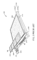
- FIG.2 is diagram illustrating the architecture and the fabrication of a touch-controlled electronic apparatus 200 according to an embodiment of the present invention.
- the touch-controlled electronic apparatus 200 includes, but is not limited to, a loading plate 2100, a touch panel 2300, a flexible printed circuit board (PCB) 2200, a sensor pad 240, and a control circuit 250.
- the loading plate 2100 has a third plane 2100A and a fourth plane 2100B opposite to the third plane 2100A, wherein the third plane 2100A is divided into a display touch area 2110, a wire area 2130, and a first hot bonding area 2140.
- the touch panel 2300 is disposed on the display touch area 2110 of the loading plate 2100, for displaying images and receiving a first touch to generate a first touch signal.
- the flexible PCB 2200 has a first plane 2200A and a second plane 2200B opposite to the first plane 2200A. Please also refer to FIG.3.
- FIG.3 (including 3A and 3B) illustrates a top view and a bottom view of the flexible PCB 2200 shown in FIG.2 .
- the first plane 2200A of the flexible PCB 2200 is divided into at least a touch button area 2210 and a control circuit area 2220.
- the sensor pad 240 is disposed on the touch button area 2210 of the flexible PCB 2200, and is used as a touch button for detecting a second touch to generate a second touch signal.
- the control circuit 250 is disposed on the control circuit area 2220 of the first plane 2200A of the flexible PCB 2200 and electronically connected to the touch panel 2300 and the sensor pad 240, for reading the first touch signal as well as the second touch signal to respectively generate a first control signal as well as a second control signal, and for determining a first position of the first touch and a second position of the second touch according to the first control signal and the second control signal, respectively.
- the second plane 2200B of the flexible PCB 2200 has a second hot bonding area 2230.
- the second plane 2200B of the flexible PCB 2200 contacts and bonds to the third plane 2100A of the loading plate 2100 (as is shown in FIG.2 ), such that the second hot bonding area 2230 overlays the first hot bonding area 2140.
- a first contact pad 260 is disposed on the first hot bonding area 2140 of the loading plate 2100 (as is shown in FIG.2 ), and a second contact pad 270 is disposed on the second hot bonding area 2230 of the flexible PCB 2200 (as is shown in 3B).
- the first contact pad 260 is hot bonded to the second contact pad 270, such that the control circuit 250 is able to electrically connected to the touch panel 230 via the first contact pad 260 and the second contact pad 270.
- the flexible PCB 2200 is disposed and bonded to the loading plate 2100
- the touch button area 2210 of the flexible PCB 2200 is disposed on at least one of the wire area 2130 and the first hot bonding area 2140 of the loading plate 2100.
- the touch button area 2210 overlays both the wire area 2130 and the first hot bonding area 2140, such that the sensing area of the touch button can be maximized in order to get a better sensor sensitivity.
- this is not meant to be a limitation of the present invention.
- the touch button area 2210 may overlay the wire area 2130, the first hot bonding area 2140, and a part of the display touch area 2110, which also belongs to the scope of the present invention.
- the abovementioned touch-controlled electronic apparatus 200 can be a mobile phone, a personal digital assistant (PDA), a PDA phone or a smart phone. But this should not be considered as limitations of the present invention, and the touch-controlled electronic apparatus 200 can be a touch-controlled electronic apparatus of other types.
- the sensor pad 240 can be composed of a copper material, and the copper material may include a particular conductive pattern, but the present invention is not limited to this only.
- the touch-controlled electronic apparatus disclosed in the present invention utilizes the flexible PCB 2200 to design touch buttons on it (i.e., the touch button area 2210). Since the touch button area 2210 overlays at least the wire area 2130 and the first hot bonding area 2140, the display touch area 2110 can be maximized and the sensing area of the touch button area 2210 can be significantly improved under a fixed-scaled touch panel. Besides, the touch buttons disclosed in the present invention adopt a design of flat buttons, which can confirm to considerations of industrial designs and product appearance.
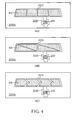
- FIG.4 is a diagram illustrating exemplary embodiments of the particular conductive patterns of the sensor pad 240 shown in FIG.2 .
- the particular conductive patterns of the sensor pad 240 can be a square (such as the particular conductive pattern 410 shown in 4A), a triangle (such as the particular conductive pattern 420 shown in 4B), or an irregular shape (such as the particular conductive pattern 430 shown in 4C). That is to say, the particular conductive patterns of the sensor pad 240 are not limited.
- Those skilled in the art should appreciate that various modifications of the particular conductive patterns of the sensor pad 240 may be made, which can be designed depending upon actual demands.
- FIG.5 is a flowchart illustrating a method for fabrication a touch-controlled electronic apparatus according to an exemplary embodiment of the present invention. Please note that the following steps are not limited to be performed according to the exact sequence shown in FIG.5 if a roughly identical result can be obtained.
- the method includes, but is not limited to, the following steps:
- Step 500 Start.
- Step 502 Provide a loading plate having a display touch area, a wire area, and a first hot bonding area.
- Step 504 Dispose a touch panel on the display touch area of the loading plate.
- Step 506 Provide a flexible PCB having at least a touch button area and a control circuit area.
- Step 508 Dispose a sensor pad on the touch button area of the flexible PCB, wherein the sensor pad is used as a touch button.
- Step 510 Dispose a control circuit on the control circuit area of the flexible PCB.
- Step 512 Dispose and bond the flexible PCB to the loading plate, such that the touch button area is disposed on at least one of the wire area and the first hot bonding area.
- Step 514 Electronically connect the control circuit to the touch panel and the sensor pad.
- the loading plate 2100 is provided, and the third plane 2100A of the loading plate 2100 has the display touch area 2110, the wire area 2130, and the first hot bonding area 2140 (the step 502).
- the touch panel 2300 is disposed on the display touch area 2110 of the loading plate 2100 (the step 504).
- the flexible PCB 2200 is provided, and the first plane 2200A of the flexible PCB 2200 has at least the touch button area 2210 and the control circuit area 2220 (the step 506).
- the sensor pad 240 is disposed on the touch button area 2210 of the flexible PCB 2200, and is used as touch buttons (the step 508).
- the control circuit 250 is disposed on the control circuit area 2220 of the flexible PCB 2200(the step 510).
- the flexible PCB 2200 is disposed and bonded to the loading plate 2100, such that the touch button area 2210 can be disposed on at least one of the wire area 2130 and the first hot bonding area 2140 (the step 512).
- the touch button area 2210 overlays both the wire area 2130 and the first hot bonding area 2140.
- the control circuit 250 is electronically connected to touch panel 2300 (for example, the first contact pad 260 and the second contact pad 270 can be utilized for electronically connecting the control circuit 250 to the touch panel 2300) and the sensor pad 240 (the step 514).
- the present invention provides a touch-controlled electronic apparatus and a related fabricating method.
- a flexible PCB is utilized in the touch-controlled electronic apparatus disclosed in the present invention so as to design the touch buttons on it (i.e., the touch button area 2210). Since the touch button area 2210 overlays at least the wire area 2130 and the first hot bonding area 2140 of the loading plate 2100, the display touch area 2110 can be maximized and the sensing area of the touch button area 2210 can be significantly improved to obtain a better sensor sensitivity under a fixed-scaled touch panel. Besides, by collocating the touch-controlled electronic apparatus together with its fabrication disclosed in the present invention, traditional mechanical buttons can be replaced and a design of flat touch buttons can be achieved, which can confirm to considerations of industrial designs and product appearance.
Landscapes
- Engineering & Computer Science (AREA)
- General Engineering & Computer Science (AREA)
- Theoretical Computer Science (AREA)
- Human Computer Interaction (AREA)
- Physics & Mathematics (AREA)
- General Physics & Mathematics (AREA)
- Computer Networks & Wireless Communication (AREA)
- Position Input By Displaying (AREA)
- Push-Button Switches (AREA)
Abstract
Description
- The present invention relates to a touch-controlled electronic apparatus and a related fabricating method according to the pre-characterizing clauses of claims 1 and 8.
- In today's consumer electronics markets, portable electronic products such as personal digital assistants (PDAs), mobile phones, and PDA phones have already adopted a touch panel as their interface tool for data communication. Currently, the electronic products are usually designed with the trend of light weight and small size, hence there is no enough space to accommodate traditional input devices such as keyboards or mice. Furthermore, most of the physical mechanical buttons, such as metal dome keypads, hardwire switches, or resistive buttons, usually have demands for a fixed height, and moving elements are required to be disposed on the surface of the electronic products in order to provide actuations to the mechanical buttons. However, these mechanical buttons will not only increase the thickness of the electronic products but also cause problems of surface discontinuity. For this reason, designs with flat buttons can be adopted to replace the conventional mechanical buttons.
- Nowadays, a capacitive touch panel is commonly used for implementing the flat buttons, which can provide touch functions of both a touch display area and a touch button area at the same time. However, conductive patterns (e.g., conductive patterns composed of indium tin oxide (ITO) or indium zinc oxide (IZO)) of the current capacitive touch panel are electronically connected with its controller by utilizing silver wires surrounded the touch panel, so that the capacitive sensor differences of the conductive patterns can be calculated by the controller in order to obtain the position of touches. Because the touch buttons cannot overlay the abovementioned "sliver wires", that is, a touch button area cannot overlay a wire area, the size of touch button area will cause the obstruction in designing the appearance and the length of the electronic products. For a fixed-scaled touch panel, the width of the wire area will be increased if the display touch area gets larger. For this reason, the touch button area will be constricted. The smaller touch button area will cause the sensor area is too small, which leads to a poor sensor sensitivity.
- Hence, how to provide the display touch area and the touch button area with a larger area, and how to solve erroneous sensing problems of touch buttons under considerations of a fixed-scaled touch panel and industrial designs, have become an important topic of designing the touch-controlled electronic apparatus.
- This in mind, the present invention aims at providing a touch-controlled electronic apparatus and a related fabricating method that solves erroneous sensing problems of touch buttons under considerations of a fixed-scaled touch panel and industrial designs.
- This is achieved by a touch-controlled electronic apparatus and a related fabricating method according to claims 1 and 8. The dependent claims pertain to corresponding further developments and improvements.
- As will be seen more clearly from the detailed description following below, the claimed a touch-controlled electronic apparatus includes a loading plate, a touch panel, a flexible PCB, a sensor pad, and a control circuit. The loading plate has a display touch area, a wire area, and a first hot bonding area. The touch panel is disposed on the display touch area of the loading plate, for displaying images and receiving a first touch to generate a first touch signal. The flexible PCB has at least a touch button area and a control circuit area. The sensor pad is disposed on the touch button area of the flexible PCB, and is used as a touch button for detecting a second touch to generate a second touch signal. The control circuit is disposed on the control circuit area of the flexible PCB and electronically connected to the touch panel and the sensor pad, for reading the first touch signal as well as the second touch signal to respectively generate a first control signal as well as a second control signal, and for determining a first position of the first touch and a second position of the second touch according to the first control signal and the second control signal, respectively. The flexible PCB is disposed and bonded to the loading plate, and the touch button area is disposed on at least one of the wire area and the first hot bonding area.
- In addition, as will be seen more clearly from the detailed description following below, the claimed method includes the steps of: providing a loading plate having a display touch area, a wire area, and a first hot bonding area; disposing a touch panel on the display touch area of the loading plate; providing a flexible PCB having at least a touch button area and a control circuit area; disposing a sensor pad on the touch button area of the flexible PCB, wherein the sensor pad is used as a touch button; disposing a control circuit on the control circuit area of the flexible PCB, and electronically connecting the control circuit to the touch panel and the sensor pad; and disposing and bonding the flexible PCB to the loading plate, such that the touch button area is disposed on at least one of the wire area and the first hot bonding area.
- In the following, the invention is further illustrated by way of example, tacking reference to the accompanying drawings. Thereof
-
FIG.1 is a diagram illustrating a touch-controlled electronic apparatus according to the prior art; -
FIG.2 is diagram illustrating the architecture and the fabrication of a touch-controlled electronic apparatus according to an embodiment of the present invention; -
FIG.3 (including 3A and 3B) illustrates a top view and a bottom view of the flexible PCB shown inFIG.2 ; -
FIG.4 (including 4A, 4B, and 4C) is a diagram illustrating exemplary embodiments of the particular conductive patterns of the sensor pad shown inFIG.2 ; and -
FIG.5 is a flowchart illustrating a method for fabrication a touch-controlled electronic apparatus according to an exemplary embodiment of the present invention. - Please refer to
FIG.1. FIG.1 is a diagram illustrating a touch-controlledelectronic apparatus 100 according to the prior art. InFIG.1 , the touch-controlledelectronic apparatus 100 includes aloading plate 1100 and a touch panel (in order to clearly present the figure, the touch panel is not marked inFIG.1 ). Theloading plate 1100 has adisplay touch area 1110, atouch button area 1120, awire area 1130, and ahot bonding area 1140. In the traditional method of work, the touch panel is disposed on both thedisplay touch area 1110 and thetouch button area 1120 of theloading board 1100. That is to say, a part of the touch panel is used for displaying images (i.e., the part of touch panel disposed upon the display touch area 1110), while another part of the touch panel is used as touch buttons (i.e., the part of the touch panel disposed upon the touch button 1120). As mentioned above, conductive patterns (e.g., conductive patterns composed of ITO or IZO) of the current capacitive touch panel are electronically connected with its controller by utilizing silver wires surrounded the touch panel, so that the capacitive sensor differences of the conductive patterns can be calculated by the controller in order to obtain the position of touches. Because the touch buttons cannot overlay the abovementioned "sliver wires", that is, thetouch button area 1120 cannot overlay thewire area 1130, the size of touch button area will cause the obstruction in designing the appearance and the length of the electronic products, as is shown inFIG.1 . For a fixed-scaled touch panel, the width of thewire area 1130 will be increased if thedisplay touch area 1110 gets larger. For this reason, thetouch button area 1120 will be constricted. The smallertouch button area 1120 will cause the sensor area is too small, which leads to a poor sensor sensitivity. - Please refer to
FIG.2. FIG.2 is diagram illustrating the architecture and the fabrication of a touch-controlledelectronic apparatus 200 according to an embodiment of the present invention. As shown inFIG.2 , the touch-controlledelectronic apparatus 200 includes, but is not limited to, aloading plate 2100, atouch panel 2300, a flexible printed circuit board (PCB) 2200, asensor pad 240, and acontrol circuit 250. Theloading plate 2100 has athird plane 2100A and afourth plane 2100B opposite to thethird plane 2100A, wherein thethird plane 2100A is divided into adisplay touch area 2110, awire area 2130, and a firsthot bonding area 2140. Thetouch panel 2300 is disposed on thedisplay touch area 2110 of theloading plate 2100, for displaying images and receiving a first touch to generate a first touch signal. - In addition, the flexible PCB 2200 has a
first plane 2200A and asecond plane 2200B opposite to thefirst plane 2200A. Please also refer toFIG.3. FIG.3 (including 3A and 3B) illustrates a top view and a bottom view of theflexible PCB 2200 shown inFIG.2 . As shown in 3A, thefirst plane 2200A of the flexible PCB 2200 is divided into at least atouch button area 2210 and acontrol circuit area 2220. Moreover, thesensor pad 240 is disposed on thetouch button area 2210 of theflexible PCB 2200, and is used as a touch button for detecting a second touch to generate a second touch signal. Thecontrol circuit 250 is disposed on thecontrol circuit area 2220 of thefirst plane 2200A of theflexible PCB 2200 and electronically connected to thetouch panel 2300 and thesensor pad 240, for reading the first touch signal as well as the second touch signal to respectively generate a first control signal as well as a second control signal, and for determining a first position of the first touch and a second position of the second touch according to the first control signal and the second control signal, respectively. As shown in 3B, thesecond plane 2200B of the flexible PCB 2200 has a secondhot bonding area 2230. Be noted that thesecond plane 2200B of theflexible PCB 2200 contacts and bonds to thethird plane 2100A of the loading plate 2100 (as is shown inFIG.2 ), such that the secondhot bonding area 2230 overlays the firsthot bonding area 2140. - Moreover, a
first contact pad 260 is disposed on the firsthot bonding area 2140 of the loading plate 2100 (as is shown inFIG.2 ), and asecond contact pad 270 is disposed on the secondhot bonding area 2230 of the flexible PCB 2200 (as is shown in 3B). Thefirst contact pad 260 is hot bonded to thesecond contact pad 270, such that thecontrol circuit 250 is able to electrically connected to the touch panel 230 via thefirst contact pad 260 and thesecond contact pad 270. - What calls for special attention is that: the flexible PCB 2200 is disposed and bonded to the
loading plate 2100, and thetouch button area 2210 of the flexible PCB 2200 is disposed on at least one of thewire area 2130 and the firsthot bonding area 2140 of theloading plate 2100. In this embodiment, thetouch button area 2210 overlays both thewire area 2130 and the firsthot bonding area 2140, such that the sensing area of the touch button can be maximized in order to get a better sensor sensitivity. But this is not meant to be a limitation of the present invention. Those skilled in the art should appreciate that various modifications to the covering range of thetouch button area 2210 may be made without departing from the spirit of the present invention, which can be designed depending upon actual demands. For example, in other embodiment, thetouch button area 2210 may overlay thewire area 2130, the firsthot bonding area 2140, and a part of thedisplay touch area 2110, which also belongs to the scope of the present invention. - Please note that the abovementioned touch-controlled
electronic apparatus 200 can be a mobile phone, a personal digital assistant (PDA), a PDA phone or a smart phone. But this should not be considered as limitations of the present invention, and the touch-controlledelectronic apparatus 200 can be a touch-controlled electronic apparatus of other types. Moreover, thesensor pad 240 can be composed of a copper material, and the copper material may include a particular conductive pattern, but the present invention is not limited to this only. - In one wore, the touch-controlled electronic apparatus disclosed in the present invention utilizes the
flexible PCB 2200 to design touch buttons on it (i.e., the touch button area 2210). Since thetouch button area 2210 overlays at least thewire area 2130 and the firsthot bonding area 2140, thedisplay touch area 2110 can be maximized and the sensing area of thetouch button area 2210 can be significantly improved under a fixed-scaled touch panel. Besides, the touch buttons disclosed in the present invention adopt a design of flat buttons, which can confirm to considerations of industrial designs and product appearance. - Please refer to
FIG.4. FIG.4 (including 4A, 4B, and 4C) is a diagram illustrating exemplary embodiments of the particular conductive patterns of thesensor pad 240 shown inFIG.2 . As can be known fromFIG.4 , the particular conductive patterns of thesensor pad 240 can be a square (such as the particularconductive pattern 410 shown in 4A), a triangle (such as the particularconductive pattern 420 shown in 4B), or an irregular shape (such as the particularconductive pattern 430 shown in 4C). That is to say, the particular conductive patterns of thesensor pad 240 are not limited. Those skilled in the art should appreciate that various modifications of the particular conductive patterns of thesensor pad 240 may be made, which can be designed depending upon actual demands. - Please refer to
FIG.5. FIG.5 is a flowchart illustrating a method for fabrication a touch-controlled electronic apparatus according to an exemplary embodiment of the present invention. Please note that the following steps are not limited to be performed according to the exact sequence shown inFIG.5 if a roughly identical result can be obtained. The method includes, but is not limited to, the following steps: - Step 502: Provide a loading plate having a display touch area, a wire area, and a first hot bonding area.
- Step 504: Dispose a touch panel on the display touch area of the loading plate. Step 506: Provide a flexible PCB having at least a touch button area and a control circuit area.
- Step 508: Dispose a sensor pad on the touch button area of the flexible PCB, wherein the sensor pad is used as a touch button.
- Step 510: Dispose a control circuit on the control circuit area of the flexible PCB. Step 512: Dispose and bond the flexible PCB to the loading plate, such that the touch button area is disposed on at least one of the wire area and the first hot bonding area.
- Step 514: Electronically connect the control circuit to the touch panel and the sensor pad.
- In the following descriptions, how to fabricate the touch-controlled
electronic apparatus 200 can be known by collocating the steps shown inFIG.5 and the elements shown inFIG.2 andFIG.3 . First, theloading plate 2100 is provided, and thethird plane 2100A of theloading plate 2100 has thedisplay touch area 2110, thewire area 2130, and the first hot bonding area 2140 (the step 502). After that, thetouch panel 2300 is disposed on thedisplay touch area 2110 of the loading plate 2100 (the step 504). Theflexible PCB 2200 is provided, and thefirst plane 2200A of theflexible PCB 2200 has at least thetouch button area 2210 and the control circuit area 2220 (the step 506). After that, thesensor pad 240 is disposed on thetouch button area 2210 of theflexible PCB 2200, and is used as touch buttons (the step 508). Furthermore, thecontrol circuit 250 is disposed on thecontrol circuit area 2220 of the flexible PCB 2200(thestep 510).Theflexible PCB 2200 is disposed and bonded to theloading plate 2100, such that thetouch button area 2210 can be disposed on at least one of thewire area 2130 and the first hot bonding area 2140 (the step 512). Preferably, thetouch button area 2210 overlays both thewire area 2130 and the firsthot bonding area 2140. Finally, thecontrol circuit 250 is electronically connected to touch panel 2300 (for example, thefirst contact pad 260 and thesecond contact pad 270 can be utilized for electronically connecting thecontrol circuit 250 to the touch panel 2300) and the sensor pad 240 (the step 514). - Please note that, the steps of the abovementioned flowchart are merely practicable embodiments of the present invention, and in no way should be considered to be limitations of the scope of the present invention. The method can include other intermediate steps or several steps can be merged into a single step without departing from the spirit of the present invention.
- The abovementioned embodiments are presented merely for describing features of the present invention, and in no way should be considered to be limitations of the scope of the present invention. In summary, the present invention provides a touch-controlled electronic apparatus and a related fabricating method. A flexible PCB is utilized in the touch-controlled electronic apparatus disclosed in the present invention so as to design the touch buttons on it (i.e., the touch button area 2210). Since the
touch button area 2210 overlays at least thewire area 2130 and the firsthot bonding area 2140 of theloading plate 2100, thedisplay touch area 2110 can be maximized and the sensing area of thetouch button area 2210 can be significantly improved to obtain a better sensor sensitivity under a fixed-scaled touch panel. Besides, by collocating the touch-controlled electronic apparatus together with its fabrication disclosed in the present invention, traditional mechanical buttons can be replaced and a design of flat touch buttons can be achieved, which can confirm to considerations of industrial designs and product appearance. - All combinations and sub-combinations of above-described features also belong to the invention.
Claims (11)
- A touch-controlled electronic apparatus ( 200 ), comprising:a loading plate ( 2100 ), having a display touch area(2110), a wire area ( 2130 ), and a first hot bonding area ( 2140 ) ;a touch panel ( 2300 ), disposed on the display touch area ( 2110 ) of the loading plate ( 2100 ), for displaying images and receiving a first touch to generate a first touch signal;characterized by:a flexible printed circuit board (PCB)( 2200 ), having at least a touch button area ( 2210 ) and a control circuit area ( 2220 ) ;a sensor pad ( 240 ), disposed on the touch button area ( 2210 ) of the flexible PCB ( 2200 ), and used as a touch button for detecting a second touch to generate a second touch signal; anda control circuit ( 250 ), disposed on the control circuit area ( 2220 ) of the flexible PCB ( 2200 ) and electronically connected to the touch panel ( 2300 ) and the sensor pad ( 240 ), for reading the first touch signal as well as the second touch signal to respectively generate a first control signal as well as a second control signal, and for determining a first position of the first touch and a second position of the second touch according to the first control signal and the second control signal, respectively;wherein the flexible PCB ( 2200 ) is disposed and bonded to the loading plate ( 2100 ), and the touch button area ( 2210 ) is disposed on at least one of the wire area ( 2130 ) and the first hot bonding area ( 2140 ).
- The touch-controlled electronic apparatus ( 200 ) of claim 1, characterized in that the flexible PCB ( 2200 ) comprises a first plane ( 2200A ) and a second plane ( 2200B ) opposite to the first plane ( 2200A ), and the first plane ( 2200A ) is divided into the touch button area ( 2210 ) and the control circuit area ( 2220 ).
- The touch-controlled electronic apparatus ( 200 ) of claim 2, characterized in that the loading plate ( 2100 ) comprises a third plane ( 2100A ) and a fourth plane ( 2100B ) opposite to the third plane ( 2100A ); the third plane (2100A) is divided into the display touch area ( 2110 ), the wire area ( 2130 ), and the first hot bonding area ( 2140 ); and the second plane (2200B) of the flexible PCB ( 2200 ) contacts and bonds to the third plane ( 2100A ) of the loading plate ( 2100 ).
- The touch-controlled electronic apparatus (200) of claim 2, characterized in that the flexible PCB ( 2200 ) further comprises a second hot bonding area ( 2230 ), and the second hot bonding area ( 2230 ) is located on the second plane ( 2200B ) and overlays the first hot bonding area ( 2140 ).
- The touch-controlled electronic apparatus (200) of claim 4, characterized in that the touch-controlled electronic apparatus ( 200 ) further comprises:a first contact pad ( 260 ), disposed on the first hot bonding area ( 2140 ) ; anda second contact pad ( 270 ), disposed on the second hot bonding area ( 2230 ) ;wherein the first contact pad ( 260 ) bonds to the second contact pad ( 270 ), and the control circuit ( 250 ) is electrically connected to the touch panel ( 2300 ) via the first contact pad ( 260 ) and the second contact pad ( 270 ).
- The touch-controlled electronic apparatus (200) of claim 1, characterized in that the sensor pad ( 240 ) is composed of a copper material, and the copper material comprises a particular conductive pattern.
- The touch-controlled electronic apparatus ( 200 ) of claim 1, characterized in that the touch-controlled electronic apparatus ( 200 ) is a mobile phone, a personal digital assistant (PDA), a PDA phone, or a smart phone.
- A method for fabricating a touch-controlled electronic apparatus ( 200 ), comprising the steps of:providing a loading plate (2100) having a display touch area ( 2110 ), a wire area ( 2130 ) , and a first hot bonding area ( 2140 ) ;disposing a touch panel ( 2300 ) on the display touch area ( 2110 ) of the loading plate ( 2100 ) ;characterized by:providing a flexible PCB ( 2200 ) having at least a touch button area( 2210 ) and a control circuit area (2220) ;disposing a sensor pad (240) on the touch button area (2210) of the flexible PCB ( 2200 ) , wherein the sensor pad ( 240 ) is used as a touch button;disposing a control circuit ( 250 ) on the control circuit area ( 2220 ) of the flexible PCB ( 2200 ), and electronically connecting the control circuit ( 250 ) to the touch panel ( 2300 ) and the sensor pad ( 240 ) ; anddisposing and bonding the flexible PCB ( 2200 ) to the loading plate ( 2100 ), such that the touch button area ( 2210 ) is disposed on at least one of the wire area ( 2130 ) and the first hot bonding area ( 2140 ).
- The method of claim 8, characterized in that the flexible PCB( 2200 ) comprises a first plane ( 2200A ) and a second plane (2200B) opposite to the first plane ( 2200A ), and the first plane ( 2200A ) is divided into the touch button area (2210) and the control circuit area ( 2220 ) ; the loading plate (2100) comprises a third plane ( 2100A ) and a fourth plane ( 2100B ) opposite to the third plane ( 2100A ), and the third plane (2100A) is divided into the display touch area ( 2110 ), the wire area ( 2130 ), and the first hot bonding area ( 2140 ) ; and the method further comprises the step of:making the second plane ( 2200B ) of the flexible PCB ( 2200 ) contact and bond to the third plane ( 2100A ) of the loading plate ( 2100 ).
- The method of claim 9, characterized in that the flexible PCB ( 2200 ) further comprises a second hot bonding area ( 2230 )located on the second plane( 2200B ); and the method further comprises the step of:disposing and bonding the flexible PCB ( 2200 ) to the loading plate ( 2100 ), such that the second hot bonding area ( 2230 ) overlays the first hot bonding area ( 2140 ).
- The method of claim 10, characterized in that the touch-controlled electronic apparatus ( 200 ) further comprises a first contact pad ( 260 ) and a second contract pad ( 270 ), being respectively disposed on the first hot bonding area (2140) and the second hot bonding area ( 2230 ) ; and the method further comprises the step of:disposing and bonding the flexible PCB ( 2200 ) on the loading plate ( 2100 ), and bonding the first contact pad ( 260 ) and the second contact pad ( 270 ) ; andelectrically connecting the control circuit ( 250 ) to the touch panel ( 2300 ) by utilizing the first contact pad ( 260 ) and the second contact pad ( 270 ).
Applications Claiming Priority (1)
| Application Number | Priority Date | Filing Date | Title |
|---|---|---|---|
| TW099114071A TWI420364B (en) | 2010-05-03 | 2010-05-03 | Touch-controlled electronic apparatus and related assembly method |
Publications (2)
| Publication Number | Publication Date |
|---|---|
| EP2385447A1 true EP2385447A1 (en) | 2011-11-09 |
| EP2385447B1 EP2385447B1 (en) | 2013-04-24 |
Family
ID=44292184
Family Applications (1)
| Application Number | Title | Priority Date | Filing Date |
|---|---|---|---|
| EP10009652.8A Not-in-force EP2385447B1 (en) | 2010-05-03 | 2010-09-15 | Touch-controlled electronic apparatus and related assembly method |
Country Status (3)
| Country | Link |
|---|---|
| US (1) | US8866755B2 (en) |
| EP (1) | EP2385447B1 (en) |
| TW (1) | TWI420364B (en) |
Cited By (1)
| Publication number | Priority date | Publication date | Assignee | Title |
|---|---|---|---|---|
| EP2610938A3 (en) * | 2011-12-30 | 2016-07-27 | Samsung Electronics Co., Ltd. | Organic light-emitting display panel and display apparatus having the same |
Families Citing this family (17)
| Publication number | Priority date | Publication date | Assignee | Title |
|---|---|---|---|---|
| TWI420364B (en) * | 2010-05-03 | 2013-12-21 | Htc Corp | Touch-controlled electronic apparatus and related assembly method |
| KR101945442B1 (en) | 2011-12-19 | 2019-02-08 | 엘지디스플레이 주식회사 | Bonding Apparatus for Manufacturing Touch Panel |
| TWI462069B (en) | 2011-12-30 | 2014-11-21 | Au Optronics Corp | Touch display panel |
| KR101400298B1 (en) * | 2012-06-14 | 2014-06-27 | 삼성디스플레이 주식회사 | Display device |
| KR101796812B1 (en) * | 2013-02-15 | 2017-11-10 | 엘지디스플레이 주식회사 | Flexible organic light emitting display device and method of manufacturing the same |
| US9740035B2 (en) | 2013-02-15 | 2017-08-22 | Lg Display Co., Ltd. | Flexible organic light emitting display device and method for manufacturing the same |
| TWI509479B (en) * | 2013-05-02 | 2015-11-21 | Pegatron Corp | Touch electronic device and touch module thereof |
| KR101452302B1 (en) | 2013-07-29 | 2014-10-22 | 주식회사 하이딥 | Touch sensor panel |
| KR101681305B1 (en) * | 2014-08-01 | 2016-12-02 | 주식회사 하이딥 | Touch input device |
| US9224790B2 (en) * | 2013-11-13 | 2015-12-29 | Industrial Technology Research Institute | Illumination device |
| KR101712346B1 (en) | 2014-09-19 | 2017-03-22 | 주식회사 하이딥 | Touch input device |
| CN104898873A (en) * | 2014-03-06 | 2015-09-09 | 宝宸(厦门)光学科技有限公司 | Touch control panel |
| JP6527343B2 (en) | 2014-08-01 | 2019-06-05 | 株式会社 ハイディープHiDeep Inc. | Touch input device |
| CN204808294U (en) * | 2015-07-10 | 2015-11-25 | 成都京东方光电科技有限公司 | Display panel and display device |
| TWI594169B (en) * | 2016-02-05 | 2017-08-01 | 宏達國際電子股份有限公司 | Touch panel assembly and portable electronic device |
| CN110989231A (en) * | 2019-11-25 | 2020-04-10 | Tcl华星光电技术有限公司 | Polarizers and Display Panels |
| CN116149093B (en) * | 2023-04-23 | 2023-07-07 | 深圳赛仕电子科技有限公司 | Breakage-proof TFT display panel bearing device |
Citations (3)
| Publication number | Priority date | Publication date | Assignee | Title |
|---|---|---|---|---|
| US20090244029A1 (en) * | 2008-03-25 | 2009-10-01 | Chun-Chung Huang | Equalized capacitive touchpad and touch positioning mehtod |
| US20090255737A1 (en) * | 2008-03-19 | 2009-10-15 | Egalax_Empia Technology Inc. | Device and Method for Preventing the Influence of Conducting Material from Point Detection of Projected Capacitive Touch Panel |
| US20100033443A1 (en) * | 2008-08-06 | 2010-02-11 | Hitachi Displays, Ltd. | Display device |
Family Cites Families (20)
| Publication number | Priority date | Publication date | Assignee | Title |
|---|---|---|---|---|
| CN100416472C (en) * | 2002-07-16 | 2008-09-03 | 阿尔卑斯电气株式会社 | Capacitive coordinate input device |
| KR100480154B1 (en) * | 2002-08-30 | 2005-04-06 | 엘지.필립스 엘시디 주식회사 | Touch Panel |
| US20070022548A1 (en) * | 2005-08-01 | 2007-02-01 | High Voltage Graphics, Inc. | Process for heat setting polyester fibers for sublimation printing |
| US7932898B2 (en) * | 2005-09-20 | 2011-04-26 | Atmel Corporation | Touch sensitive screen |
| US8004497B2 (en) * | 2006-05-18 | 2011-08-23 | Cypress Semiconductor Corporation | Two-pin buttons |
| US8169421B2 (en) * | 2006-06-19 | 2012-05-01 | Cypress Semiconductor Corporation | Apparatus and method for detecting a touch-sensor pad gesture |
| US8026903B2 (en) * | 2007-01-03 | 2011-09-27 | Apple Inc. | Double-sided touch sensitive panel and flex circuit bonding |
| CN101470578A (en) | 2007-12-27 | 2009-07-01 | 英业达股份有限公司 | Touch control electronic device and operation method thereof |
| TWM337793U (en) * | 2008-02-26 | 2008-08-01 | Mildex Optical Inc | Fully planar touch panel |
| TWI365013B (en) * | 2008-05-23 | 2012-05-21 | Au Optronics Corp | Flat panel display |
| US8159777B2 (en) * | 2008-06-19 | 2012-04-17 | Apple Inc. | Portable electronic device with multipurpose hard drive circuit board |
| US20110134075A1 (en) * | 2008-08-07 | 2011-06-09 | Sharp Kabushiki Kaisha | Touch panel, display, and electronic device |
| CN101441516B (en) | 2008-12-25 | 2011-11-09 | 联想移动通信科技有限公司 | Handhold equipment and substrate for the same |
| US8576161B2 (en) * | 2009-06-18 | 2013-11-05 | Apple Inc. | Driving an OLED display structure integrated with a touch sensor configuration |
| TWM375245U (en) * | 2009-07-30 | 2010-03-01 | Minlad Invest Ltd | Resistance touch panel |
| TWM374607U (en) * | 2009-08-27 | 2010-02-21 | Minlad Invest Ltd | Resistive touch panel structure |
| US8421890B2 (en) * | 2010-01-15 | 2013-04-16 | Picofield Technologies, Inc. | Electronic imager using an impedance sensor grid array and method of making |
| US8574964B2 (en) * | 2010-04-14 | 2013-11-05 | Stats Chippac, Ltd. | Semiconductor device and method of forming electrical interconnection between semiconductor die and substrate with continuous body of solder tape |
| US20110254758A1 (en) * | 2010-04-19 | 2011-10-20 | Qualcomm Mems Technologies, Inc. | Flex Design and Attach Method for Reducing Display Panel Periphery |
| TWI420364B (en) * | 2010-05-03 | 2013-12-21 | Htc Corp | Touch-controlled electronic apparatus and related assembly method |
-
2010
- 2010-05-03 TW TW099114071A patent/TWI420364B/en not_active IP Right Cessation
- 2010-08-25 US US12/862,796 patent/US8866755B2/en not_active Expired - Fee Related
- 2010-09-15 EP EP10009652.8A patent/EP2385447B1/en not_active Not-in-force
Patent Citations (3)
| Publication number | Priority date | Publication date | Assignee | Title |
|---|---|---|---|---|
| US20090255737A1 (en) * | 2008-03-19 | 2009-10-15 | Egalax_Empia Technology Inc. | Device and Method for Preventing the Influence of Conducting Material from Point Detection of Projected Capacitive Touch Panel |
| US20090244029A1 (en) * | 2008-03-25 | 2009-10-01 | Chun-Chung Huang | Equalized capacitive touchpad and touch positioning mehtod |
| US20100033443A1 (en) * | 2008-08-06 | 2010-02-11 | Hitachi Displays, Ltd. | Display device |
Cited By (1)
| Publication number | Priority date | Publication date | Assignee | Title |
|---|---|---|---|---|
| EP2610938A3 (en) * | 2011-12-30 | 2016-07-27 | Samsung Electronics Co., Ltd. | Organic light-emitting display panel and display apparatus having the same |
Also Published As
| Publication number | Publication date |
|---|---|
| US20110267284A1 (en) | 2011-11-03 |
| US8866755B2 (en) | 2014-10-21 |
| TWI420364B (en) | 2013-12-21 |
| EP2385447B1 (en) | 2013-04-24 |
| TW201140388A (en) | 2011-11-16 |
Similar Documents
| Publication | Publication Date | Title |
|---|---|---|
| US8866755B2 (en) | Touch-controlled electronic apparatus and related assembly method | |
| US8730199B2 (en) | Capacitive control panel | |
| CN101427468B (en) | Reconfigurable Tactile Sensor Input Device | |
| US7151528B2 (en) | System for disposing a proximity sensitive touchpad behind a mobile phone keypad | |
| CA2449447C (en) | System for disposing a proximity sensitive touchpad behind a mobile phone keymat | |
| JP2019521462A (en) | Electronic device equipped with complex human interface | |
| US20130285979A1 (en) | Touch device | |
| CN102236458A (en) | Touch control electronic device and related assembling method thereof | |
| CN107659699A (en) | A kind of button assembly and the intelligent terminal with the button assembly | |
| EP3195476B1 (en) | Capacitive touch sensor | |
| CN102571056A (en) | Key with touch detection function and electronic device comprising same | |
| KR20110032649A (en) | User interface unit | |
| CN105162448A (en) | Metal inductive touch device | |
| KR101583827B1 (en) | Input device | |
| CN205563362U (en) | Intelligent terminal | |
| US9195277B2 (en) | Touch panel with proximity sensor | |
| KR100718988B1 (en) | Input device of electronic device | |
| US20140138232A1 (en) | Extended keyboard, electronic device, and keyboard extending system | |
| KR102914072B1 (en) | Operation module of integrated type | |
| KR102838818B1 (en) | Terminal Device With Buttonless Side Key | |
| CN1969252A (en) | An inductive switch type user interface device and its portable terminal | |
| KR100718987B1 (en) | Input device of electronic device | |
| KR20240146468A (en) | Operation module of integrated type | |
| KR20150134656A (en) | A mesh type electrode is formed on the transparent touch sensor, and a manufacturing method | |
| CN116540897A (en) | Copper wire etching flexible circuit board structure, thin film type pressure sensor and touch device |
Legal Events
| Date | Code | Title | Description |
|---|---|---|---|
| 17P | Request for examination filed |
Effective date: 20100915 |
|
| AK | Designated contracting states |
Kind code of ref document: A1 Designated state(s): AL AT BE BG CH CY CZ DE DK EE ES FI FR GB GR HR HU IE IS IT LI LT LU LV MC MK MT NL NO PL PT RO SE SI SK SM TR |
|
| AX | Request for extension of the european patent |
Extension state: BA ME RS |
|
| 17Q | First examination report despatched |
Effective date: 20111018 |
|
| PUAI | Public reference made under article 153(3) epc to a published international application that has entered the european phase |
Free format text: ORIGINAL CODE: 0009012 |
|
| GRAP | Despatch of communication of intention to grant a patent |
Free format text: ORIGINAL CODE: EPIDOSNIGR1 |
|
| GRAS | Grant fee paid |
Free format text: ORIGINAL CODE: EPIDOSNIGR3 |
|
| GRAA | (expected) grant |
Free format text: ORIGINAL CODE: 0009210 |
|
| AK | Designated contracting states |
Kind code of ref document: B1 Designated state(s): AL AT BE BG CH CY CZ DE DK EE ES FI FR GB GR HR HU IE IS IT LI LT LU LV MC MK MT NL NO PL PT RO SE SI SK SM TR |
|
| REG | Reference to a national code |
Ref country code: GB Ref legal event code: FG4D |
|
| REG | Reference to a national code |
Ref country code: CH Ref legal event code: EP |
|
| REG | Reference to a national code |
Ref country code: AT Ref legal event code: REF Ref document number: 608965 Country of ref document: AT Kind code of ref document: T Effective date: 20130515 |
|
| REG | Reference to a national code |
Ref country code: IE Ref legal event code: FG4D |
|
| REG | Reference to a national code |
Ref country code: DE Ref legal event code: R096 Ref document number: 602010006474 Country of ref document: DE Effective date: 20130627 |
|
| REG | Reference to a national code |
Ref country code: NL Ref legal event code: T3 |
|
| REG | Reference to a national code |
Ref country code: AT Ref legal event code: MK05 Ref document number: 608965 Country of ref document: AT Kind code of ref document: T Effective date: 20130424 |
|
| REG | Reference to a national code |
Ref country code: LT Ref legal event code: MG4D |
|
| PG25 | Lapsed in a contracting state [announced via postgrant information from national office to epo] |
Ref country code: IS Free format text: LAPSE BECAUSE OF FAILURE TO SUBMIT A TRANSLATION OF THE DESCRIPTION OR TO PAY THE FEE WITHIN THE PRESCRIBED TIME-LIMIT Effective date: 20130824 Ref country code: PT Free format text: LAPSE BECAUSE OF FAILURE TO SUBMIT A TRANSLATION OF THE DESCRIPTION OR TO PAY THE FEE WITHIN THE PRESCRIBED TIME-LIMIT Effective date: 20130826 Ref country code: FI Free format text: LAPSE BECAUSE OF FAILURE TO SUBMIT A TRANSLATION OF THE DESCRIPTION OR TO PAY THE FEE WITHIN THE PRESCRIBED TIME-LIMIT Effective date: 20130424 Ref country code: ES Free format text: LAPSE BECAUSE OF FAILURE TO SUBMIT A TRANSLATION OF THE DESCRIPTION OR TO PAY THE FEE WITHIN THE PRESCRIBED TIME-LIMIT Effective date: 20130804 Ref country code: BE Free format text: LAPSE BECAUSE OF FAILURE TO SUBMIT A TRANSLATION OF THE DESCRIPTION OR TO PAY THE FEE WITHIN THE PRESCRIBED TIME-LIMIT Effective date: 20130424 Ref country code: SE Free format text: LAPSE BECAUSE OF FAILURE TO SUBMIT A TRANSLATION OF THE DESCRIPTION OR TO PAY THE FEE WITHIN THE PRESCRIBED TIME-LIMIT Effective date: 20130424 Ref country code: LT Free format text: LAPSE BECAUSE OF FAILURE TO SUBMIT A TRANSLATION OF THE DESCRIPTION OR TO PAY THE FEE WITHIN THE PRESCRIBED TIME-LIMIT Effective date: 20130424 Ref country code: AT Free format text: LAPSE BECAUSE OF FAILURE TO SUBMIT A TRANSLATION OF THE DESCRIPTION OR TO PAY THE FEE WITHIN THE PRESCRIBED TIME-LIMIT Effective date: 20130424 Ref country code: GR Free format text: LAPSE BECAUSE OF FAILURE TO SUBMIT A TRANSLATION OF THE DESCRIPTION OR TO PAY THE FEE WITHIN THE PRESCRIBED TIME-LIMIT Effective date: 20130725 Ref country code: SI Free format text: LAPSE BECAUSE OF FAILURE TO SUBMIT A TRANSLATION OF THE DESCRIPTION OR TO PAY THE FEE WITHIN THE PRESCRIBED TIME-LIMIT Effective date: 20130424 Ref country code: NO Free format text: LAPSE BECAUSE OF FAILURE TO SUBMIT A TRANSLATION OF THE DESCRIPTION OR TO PAY THE FEE WITHIN THE PRESCRIBED TIME-LIMIT Effective date: 20130724 |
|
| PG25 | Lapsed in a contracting state [announced via postgrant information from national office to epo] |
Ref country code: LV Free format text: LAPSE BECAUSE OF FAILURE TO SUBMIT A TRANSLATION OF THE DESCRIPTION OR TO PAY THE FEE WITHIN THE PRESCRIBED TIME-LIMIT Effective date: 20130424 Ref country code: CY Free format text: LAPSE BECAUSE OF FAILURE TO SUBMIT A TRANSLATION OF THE DESCRIPTION OR TO PAY THE FEE WITHIN THE PRESCRIBED TIME-LIMIT Effective date: 20130424 Ref country code: BG Free format text: LAPSE BECAUSE OF FAILURE TO SUBMIT A TRANSLATION OF THE DESCRIPTION OR TO PAY THE FEE WITHIN THE PRESCRIBED TIME-LIMIT Effective date: 20130724 Ref country code: HR Free format text: LAPSE BECAUSE OF FAILURE TO SUBMIT A TRANSLATION OF THE DESCRIPTION OR TO PAY THE FEE WITHIN THE PRESCRIBED TIME-LIMIT Effective date: 20130424 Ref country code: PL Free format text: LAPSE BECAUSE OF FAILURE TO SUBMIT A TRANSLATION OF THE DESCRIPTION OR TO PAY THE FEE WITHIN THE PRESCRIBED TIME-LIMIT Effective date: 20130424 |
|
| PG25 | Lapsed in a contracting state [announced via postgrant information from national office to epo] |
Ref country code: SK Free format text: LAPSE BECAUSE OF FAILURE TO SUBMIT A TRANSLATION OF THE DESCRIPTION OR TO PAY THE FEE WITHIN THE PRESCRIBED TIME-LIMIT Effective date: 20130424 Ref country code: DK Free format text: LAPSE BECAUSE OF FAILURE TO SUBMIT A TRANSLATION OF THE DESCRIPTION OR TO PAY THE FEE WITHIN THE PRESCRIBED TIME-LIMIT Effective date: 20130424 Ref country code: EE Free format text: LAPSE BECAUSE OF FAILURE TO SUBMIT A TRANSLATION OF THE DESCRIPTION OR TO PAY THE FEE WITHIN THE PRESCRIBED TIME-LIMIT Effective date: 20130424 Ref country code: CZ Free format text: LAPSE BECAUSE OF FAILURE TO SUBMIT A TRANSLATION OF THE DESCRIPTION OR TO PAY THE FEE WITHIN THE PRESCRIBED TIME-LIMIT Effective date: 20130424 |
|
| PG25 | Lapsed in a contracting state [announced via postgrant information from national office to epo] |
Ref country code: IT Free format text: LAPSE BECAUSE OF FAILURE TO SUBMIT A TRANSLATION OF THE DESCRIPTION OR TO PAY THE FEE WITHIN THE PRESCRIBED TIME-LIMIT Effective date: 20130424 Ref country code: RO Free format text: LAPSE BECAUSE OF FAILURE TO SUBMIT A TRANSLATION OF THE DESCRIPTION OR TO PAY THE FEE WITHIN THE PRESCRIBED TIME-LIMIT Effective date: 20130424 |
|
| PLBE | No opposition filed within time limit |
Free format text: ORIGINAL CODE: 0009261 |
|
| STAA | Information on the status of an ep patent application or granted ep patent |
Free format text: STATUS: NO OPPOSITION FILED WITHIN TIME LIMIT |
|
| 26N | No opposition filed |
Effective date: 20140127 |
|
| PG25 | Lapsed in a contracting state [announced via postgrant information from national office to epo] |
Ref country code: MC Free format text: LAPSE BECAUSE OF FAILURE TO SUBMIT A TRANSLATION OF THE DESCRIPTION OR TO PAY THE FEE WITHIN THE PRESCRIBED TIME-LIMIT Effective date: 20130424 |
|
| REG | Reference to a national code |
Ref country code: DE Ref legal event code: R097 Ref document number: 602010006474 Country of ref document: DE Effective date: 20140127 |
|
| REG | Reference to a national code |
Ref country code: IE Ref legal event code: MM4A |
|
| PG25 | Lapsed in a contracting state [announced via postgrant information from national office to epo] |
Ref country code: IE Free format text: LAPSE BECAUSE OF NON-PAYMENT OF DUE FEES Effective date: 20130915 |
|
| REG | Reference to a national code |
Ref country code: CH Ref legal event code: PCOW Free format text: NEW ADDRESS: NO. 23, XINGHUA ROAD TAOYUAN DISTRICT, TAOYUAN CITY 330 (TW) |
|
| REG | Reference to a national code |
Ref country code: CH Ref legal event code: PL |
|
| PG25 | Lapsed in a contracting state [announced via postgrant information from national office to epo] |
Ref country code: SM Free format text: LAPSE BECAUSE OF FAILURE TO SUBMIT A TRANSLATION OF THE DESCRIPTION OR TO PAY THE FEE WITHIN THE PRESCRIBED TIME-LIMIT Effective date: 20130424 |
|
| PG25 | Lapsed in a contracting state [announced via postgrant information from national office to epo] |
Ref country code: MT Free format text: LAPSE BECAUSE OF FAILURE TO SUBMIT A TRANSLATION OF THE DESCRIPTION OR TO PAY THE FEE WITHIN THE PRESCRIBED TIME-LIMIT Effective date: 20130424 Ref country code: TR Free format text: LAPSE BECAUSE OF FAILURE TO SUBMIT A TRANSLATION OF THE DESCRIPTION OR TO PAY THE FEE WITHIN THE PRESCRIBED TIME-LIMIT Effective date: 20130424 |
|
| PG25 | Lapsed in a contracting state [announced via postgrant information from national office to epo] |
Ref country code: MK Free format text: LAPSE BECAUSE OF FAILURE TO SUBMIT A TRANSLATION OF THE DESCRIPTION OR TO PAY THE FEE WITHIN THE PRESCRIBED TIME-LIMIT Effective date: 20130424 Ref country code: HU Free format text: LAPSE BECAUSE OF FAILURE TO SUBMIT A TRANSLATION OF THE DESCRIPTION OR TO PAY THE FEE WITHIN THE PRESCRIBED TIME-LIMIT; INVALID AB INITIO Effective date: 20100915 Ref country code: LU Free format text: LAPSE BECAUSE OF NON-PAYMENT OF DUE FEES Effective date: 20130915 Ref country code: LI Free format text: LAPSE BECAUSE OF NON-PAYMENT OF DUE FEES Effective date: 20140930 Ref country code: CH Free format text: LAPSE BECAUSE OF NON-PAYMENT OF DUE FEES Effective date: 20140930 |
|
| REG | Reference to a national code |
Ref country code: FR Ref legal event code: PLFP Year of fee payment: 7 |
|
| REG | Reference to a national code |
Ref country code: FR Ref legal event code: PLFP Year of fee payment: 8 |
|
| REG | Reference to a national code |
Ref country code: FR Ref legal event code: PLFP Year of fee payment: 9 |
|
| PG25 | Lapsed in a contracting state [announced via postgrant information from national office to epo] |
Ref country code: AL Free format text: LAPSE BECAUSE OF FAILURE TO SUBMIT A TRANSLATION OF THE DESCRIPTION OR TO PAY THE FEE WITHIN THE PRESCRIBED TIME-LIMIT Effective date: 20130424 |
|
| PGFP | Annual fee paid to national office [announced via postgrant information from national office to epo] |
Ref country code: DE Payment date: 20180904 Year of fee payment: 9 Ref country code: FR Payment date: 20180813 Year of fee payment: 9 |
|
| PGFP | Annual fee paid to national office [announced via postgrant information from national office to epo] |
Ref country code: GB Payment date: 20180912 Year of fee payment: 9 Ref country code: NL Payment date: 20180912 Year of fee payment: 9 |
|
| REG | Reference to a national code |
Ref country code: DE Ref legal event code: R119 Ref document number: 602010006474 Country of ref document: DE |
|
| REG | Reference to a national code |
Ref country code: NL Ref legal event code: MM Effective date: 20191001 |
|
| PG25 | Lapsed in a contracting state [announced via postgrant information from national office to epo] |
Ref country code: NL Free format text: LAPSE BECAUSE OF NON-PAYMENT OF DUE FEES Effective date: 20191001 Ref country code: DE Free format text: LAPSE BECAUSE OF NON-PAYMENT OF DUE FEES Effective date: 20200401 |
|
| GBPC | Gb: european patent ceased through non-payment of renewal fee |
Effective date: 20190915 |
|
| PG25 | Lapsed in a contracting state [announced via postgrant information from national office to epo] |
Ref country code: GB Free format text: LAPSE BECAUSE OF NON-PAYMENT OF DUE FEES Effective date: 20190915 Ref country code: FR Free format text: LAPSE BECAUSE OF NON-PAYMENT OF DUE FEES Effective date: 20190930 |