EP2381750A1 - Adhesive reinforced open hole interconnect - Google Patents
Adhesive reinforced open hole interconnect Download PDFInfo
- Publication number
- EP2381750A1 EP2381750A1 EP11152541A EP11152541A EP2381750A1 EP 2381750 A1 EP2381750 A1 EP 2381750A1 EP 11152541 A EP11152541 A EP 11152541A EP 11152541 A EP11152541 A EP 11152541A EP 2381750 A1 EP2381750 A1 EP 2381750A1
- Authority
- EP
- European Patent Office
- Prior art keywords
- pcb
- holes
- flex
- conductive material
- pads
- Prior art date
- Legal status (The legal status is an assumption and is not a legal conclusion. Google has not performed a legal analysis and makes no representation as to the accuracy of the status listed.)
- Granted
Links
Images




Classifications
-
- H—ELECTRICITY
- H05—ELECTRIC TECHNIQUES NOT OTHERWISE PROVIDED FOR
- H05K—PRINTED CIRCUITS; CASINGS OR CONSTRUCTIONAL DETAILS OF ELECTRIC APPARATUS; MANUFACTURE OF ASSEMBLAGES OF ELECTRICAL COMPONENTS
- H05K3/00—Apparatus or processes for manufacturing printed circuits
- H05K3/36—Assembling printed circuits with other printed circuits
- H05K3/361—Assembling flexible printed circuits with other printed circuits
-
- H—ELECTRICITY
- H05—ELECTRIC TECHNIQUES NOT OTHERWISE PROVIDED FOR
- H05K—PRINTED CIRCUITS; CASINGS OR CONSTRUCTIONAL DETAILS OF ELECTRIC APPARATUS; MANUFACTURE OF ASSEMBLAGES OF ELECTRICAL COMPONENTS
- H05K1/00—Printed circuits
- H05K1/02—Details
- H05K1/11—Printed elements for providing electric connections to or between printed circuits
- H05K1/118—Printed elements for providing electric connections to or between printed circuits specially for flexible printed circuits, e.g. using folded portions
-
- H—ELECTRICITY
- H05—ELECTRIC TECHNIQUES NOT OTHERWISE PROVIDED FOR
- H05K—PRINTED CIRCUITS; CASINGS OR CONSTRUCTIONAL DETAILS OF ELECTRIC APPARATUS; MANUFACTURE OF ASSEMBLAGES OF ELECTRICAL COMPONENTS
- H05K2201/00—Indexing scheme relating to printed circuits covered by H05K1/00
- H05K2201/10—Details of components or other objects attached to or integrated in a printed circuit board
- H05K2201/10613—Details of electrical connections of non-printed components, e.g. special leads
- H05K2201/10621—Components characterised by their electrical contacts
- H05K2201/10666—Plated through-hole for surface mounting on PCB
-
- H—ELECTRICITY
- H05—ELECTRIC TECHNIQUES NOT OTHERWISE PROVIDED FOR
- H05K—PRINTED CIRCUITS; CASINGS OR CONSTRUCTIONAL DETAILS OF ELECTRIC APPARATUS; MANUFACTURE OF ASSEMBLAGES OF ELECTRICAL COMPONENTS
- H05K2203/00—Indexing scheme relating to apparatus or processes for manufacturing printed circuits covered by H05K3/00
- H05K2203/04—Soldering or other types of metallurgic bonding
- H05K2203/0455—PTH for surface mount device [SMD], e.g. wherein solder flows through the PTH during mounting
-
- H—ELECTRICITY
- H05—ELECTRIC TECHNIQUES NOT OTHERWISE PROVIDED FOR
- H05K—PRINTED CIRCUITS; CASINGS OR CONSTRUCTIONAL DETAILS OF ELECTRIC APPARATUS; MANUFACTURE OF ASSEMBLAGES OF ELECTRICAL COMPONENTS
- H05K3/00—Apparatus or processes for manufacturing printed circuits
- H05K3/30—Assembling printed circuits with electric components, e.g. with resistors
- H05K3/32—Assembling printed circuits with electric components, e.g. with resistors electrically connecting electric components or wires to printed circuits
- H05K3/321—Assembling printed circuits with electric components, e.g. with resistors electrically connecting electric components or wires to printed circuits by conductive adhesives
-
- H—ELECTRICITY
- H05—ELECTRIC TECHNIQUES NOT OTHERWISE PROVIDED FOR
- H05K—PRINTED CIRCUITS; CASINGS OR CONSTRUCTIONAL DETAILS OF ELECTRIC APPARATUS; MANUFACTURE OF ASSEMBLAGES OF ELECTRICAL COMPONENTS
- H05K3/00—Apparatus or processes for manufacturing printed circuits
- H05K3/46—Manufacturing multilayer circuits
- H05K3/4611—Manufacturing multilayer circuits by laminating two or more circuit boards
- H05K3/4626—Manufacturing multilayer circuits by laminating two or more circuit boards characterised by the insulating layers or materials
- H05K3/4635—Manufacturing multilayer circuits by laminating two or more circuit boards characterised by the insulating layers or materials laminating flexible circuit boards using additional insulating adhesive materials between the boards
Definitions
- the present invention relates generally to flexible printed circuit board (PCB) assemblies and more specifically to an adhesive reinforced open hole interconnect of flexible PCBs.
- PCB printed circuit board
- the present invention is a method for interconnecting a first flex PCB with a second flex PCB.
- the method includes: providing the first flex PCB with holes at contact locations to be electrically coupled to the second flex PCB; providing the second flex PCB with electrical pads corresponding to the holes at the contact locations; applying a non-conductive material between the first PCB and the and second PCB with clearances for each of the electrical pads; aligning the first PCB with the second PCB so that the holes in the first PCB are in line with the corresponding electrical pads on the second PCB; bonding a portion of flat areas on the first and second PCBs together; dispensing a conductive adhesive into the holes to fill the space created by the holes, corresponding clearances of the non-conductive material, and the corresponding electrical pads; and curing the conductive adhesive.
- the non-conductive material may be a non-conductive adhesive film and the clearances of the non-conductive material may be cut holes in the adhesive film at the contact locations.
- the non-conductive material may be a non-conductive paste and the clearances of the non-conductive material may exclude the non-conductive paste at the contact locations.
- the present invention is a method for interconnecting a first flex PCB with a second flex PCB.
- the method includes: providing the first flex PCB with holes at contact locations to be electrically coupled to the second flex PCB; providing the second flex PCB with electrical pads corresponding to the holes at the contact locations; aligning the first PCB with the second PCB so that the holes in the first PCB are in line with the corresponding electrical pads on the second PCB; mechanically attaching the first PCB to the second PCB by fusion bonding a portion of areas of bare dielectric material on each of the first and second PCB; dispensing a conductive adhesive into the holes to fill the area created by the holes and the corresponding electrical pads; and curing the conductive adhesive.
- the present invention is a flex PCB assembly which includes: a first flex PCB including holes at electrical contact locations; a second flex PCB including electrical pads corresponding to the holes at the electrical contact locations; a non-conductive material between the first PCB and the and second PCB with clearances for each of the electrical pads; and a conductive adhesive dispensed in the holes to fill the space created by the holes, corresponding clearances of the non-conductive material, and the corresponding electrical pads to provide electrical contacts between the hole of the first PCB and the pads of the second PCB, wherein the first PCB is aligned with the second PCB so that the holes in the first PCB are in line with the corresponding electrical pads on the second PCB.
- the first flex PCB may also include conductive material at the holes with an annular ring shape. Also, the size of the pads may be larger than the size of the holes.
- the present invention is a method for interconnect of flexible PCBs using adhesive reinforced open holes and/or a PCB assembly using the same method.
- the method of the present invention facilitates bonding of two or more separate flex PCBs that only need to attach in discrete areas to make electrical connection. If these were conventional flat circuits, standard drill and plate techniques could be used. However, since these PCBs (circuits) are only bonded in discrete areas, new processes are incorporated to allow for alignment inspection and post bonding electrical connection.
- FIGs. 1A to 1C show a stack up of two open hole PCBs, according to some embodiments of the present invention.
- two PCBs are used for simplicity in the examples through out this disclosure, the present invention is not limited to two PCBs and is also applicable to more than two flexible PCBs to be interconnected.
- a top flex PCB 12 includes at least one open hole (through hole) 14 with an annular ring 11 on both sides of the PCB anywhere an electrical contact is required.
- a bottom 3-D flex PCB 16 includes at least one electrical pad 17 that corresponds to the at least one through hole 14, at each location.
- the electrical pad(s) 17 has the same or slightly larger diameter as the through holes 14 including the annular ring 11.
- the through hole 14 in the top PCB 12 is used for visual alignment of the top PCB with the bottom PCB 16, and for electrical connection of the two PCBs 12 and 16.
- the two PCBs 12 and 16 are bonded together using, for example, a non-conductive adhesive 13, which includes a cutout pad 15, to create mechanical support with clearances around the electrical connection pads 17.
- the non-conductive adhesive may be cured to strengthen the boding.
- the top PCB 12 is aligned with the bottom PCB 16 with appropriate tooling. Once in the alignment tooling, alignment is assured by inspecting to see if the holes 14 in the top PCB 12 align with the pads 17 on the bottom PCB 16.
- the non-conductive bond may be cured, for example, by heat, pressure and time. The bond provides a seal around the pads preventing conductive adhesive from squeezing in between layers, which could cause electrical shorts.
- FIG. 1B shows the two PCBs 12 and 16 assembled together.
- a conductive bond for example, a conductive paste
- the conductive paste is dispensed to fill the cavity created by the hole 14, non-conductive adhesive 13 and pad 17 ( FIG. 1 B) by syringe or dispense jetting techniques that can get in between the 3-dimensional cavities between the two PCBs.
- the top PCB 12 and the bottom PCB 16 are mechanically bonded together by any of the following methods.
- a non-conductive film may be placed onto the bottom PCB 16 with clearances around the electrical bonding pads 17 ( FIG. 2 );
- a non-conductive paste adhesive may be dispensed onto the bottom PCB 16 with clearances around the electrical bonding pads 17 ( FIG. 3 ); or base dielectric layers (e.g., flex circuit plastic) are fusion bonded together around the pads 17 ( FIG. 4 ).
- conductive adhesive is dispensed into the holes of the top circuit to fill the cavity created by the hole, non-conductive adhesive and pad on bottom ( Figure 1c ) by syringe or dispense jetting techniques that can get in between the 3-dimensional features of the circuit. Enough conductive adhesive is dispensed to fill the cavity and squeeze up onto the annular ring. The conductive adhesive is then cured to complete the electrical connections.
- circuit etching, drilling and plating are used to fabricate the circuits (PCBs) separately, however, the open hole of the top PCB may be larger than a standard via, which allows for visual inspection of the alignment with the bottom PCB and subsequent dispensing of conductive adhesive to make the electrical connections.
- the non-conductive bond used for the mechanical attachment of the two PCBs also provides a seal around the pads for electrical connection that prevents the conductive material from squeezing between circuits, which could cause electrical short circuits.
- the design of the individual PCBs is made such that the top PCB 12 contains large diameter plated through holes 14 with an annular ring of at least 0.002" on top (e.g., in FIG. 1 A) .
- the hole 14 is large enough to dispense conductive adhesive through.
- the catch electrical pad 17 on the bottom PCB 16 is made to the same or larger diameter of the outer diameter of the annular ring 11. In RF applications, the 2 diameters will most likely be substantially the same, depending on what is required for impedance matching of the system. For non-RF pads, the bottom pad could be larger to improve registration.
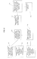
- FIG. 2 shows an exemplary process flow for interconnection of two or more PCBs with non-conductive film, according to some embodiments of the present invention.
- a top PCB is provided (e.g., designed and fabricated) with holes and (annular) rings at the attachment locations.
- a bottom PCB is provided (e.g., designed and fabricated) with pads matching the location of the pads on the top PCB at the attachment locations. Clearance for the pads in the non-conductive adhesive film is provided by pre-cutting matching holes in the non-conductive adhesive film where the electrical connections (of the two PCBs) will occur, as shown in block 206.
- the top PCB is aligned with the bottom PCB so that the hole is the top PCB are in line (aligned) with the corresponding pads on the bottom PCB.
- the non-conductive adhesive film is the aligned on the bottom PCB and tacked in place, as shown in block 210. A portion of the flat areas of the two PCBs are then bond together with, for example, heat and pressure using the non-conductive film for mechanical interconnect, as shown in block 212.
- a conductive adhesive is dispensed into the holes to fill the area created by the holes, the pads and the non-conductive film, and on top of the pads.
- the conductive adhesive is then cured by, for example, heat in block 216.
- FIG. 3 shows an exemplary process flow for interconnection of two or more PCBs with non-conductive paste, according to some embodiments of the present invention.
- a top PCB is provided (e.g., designed and fabricated) with holes and (annular) rings at the attachment locations.
- a bottom PCB is provided (e.g., designed and fabricated) with electrical pads matching the location of the pads on the top PCB at the attachment locations.
- the non-conductive paste is dispensed on the bottom PCB with clearance for the pads on the bottom PCB, as shown in block 306.
- the top PCB is aligned over the bottom PCB so that the hole in the top PCB are in line with the pads on the bottom PCB.
- a portion of the flat areas of the two PCBs are then bond together with, for example, heat and pressure to cure the non-conductive paste for mechanical interconnect, as shown in block 310.
- a conductive adhesive is dispensed into the holes to fill the area created by the holes, the pads and the non-conductive paste, on top of the pads. The conductive adhesive is then cured by, for example, heat in block 314.
- FIG. 4 shows an exemplary process flow for interconnection of two or more PCBs with fusion bond, according to some embodiments of the present invention.
- a top PCB is provided (e.g., designed and fabricated) with holes and (annular) rings at the attachment locations.
- a bottom PCB is provided (e.g., designed and fabricated) with electrical pads matching the location of the pads on the top PCB at the attachment locations.
- the top PCB is aligned over the bottom PCB so that the hole in top PCB are in line with the pads on the bottom PCB.
- the two PCBs are then mechanically attached together by fusion bonding a portion of the areas of bare dielectric material on the two PCBs in block 408.
- a conductive adhesive is dispensed into the holes to fill the area created by the holes, the pads and the non-conductive paste, on top of the pads.
- the conductive adhesive is then cured by, for example, heat in block 412.
Landscapes
- Engineering & Computer Science (AREA)
- Microelectronics & Electronic Packaging (AREA)
- Manufacturing & Machinery (AREA)
- Combinations Of Printed Boards (AREA)
Abstract

Description
- The present invention relates generally to flexible printed circuit board (PCB) assemblies and more specifically to an adhesive reinforced open hole interconnect of flexible PCBs.
- Next generation large area multifunction mixed signal printed circuit board (PCB) assembly for space and airship applications, such as, radar and communication systems need to be lighter weight and more conformal than what can be achieved with current multilayer rigid and flexible (flex) PCB assembly technology. Methods have been created and demonstrated that create antenna structures out of individual layers of flex PCBs that require electrical interconnect between one another. However, many interconnects need to align and bond to form the working circuits. Furthermore, traditional methods of electrically bonding individual layers of flex PCBs have problems with alignment of the electrical pads that require connection.
- In more recent attempts, these connections were created with a blind bond attached between pads on the two flex PCBs with dispensed conductive and non-conductive pastes. Nevertheless, in many instances, pads do not align or conductive adhesive short between adjacent pads. Moreover, issues with the quality of the bonds are not known until after the parts are cured and tested. Accordingly, extensive and expensive rework is required if the alignment is off.
- Therefore, there is a need for a more accurate and higher quality interconnect of flexible PCBs, specially in Radio Frequency (RF) range.
- In some embodiments, the present invention is a method for interconnecting a first flex PCB with a second flex PCB. The method includes: providing the first flex PCB with holes at contact locations to be electrically coupled to the second flex PCB; providing the second flex PCB with electrical pads corresponding to the holes at the contact locations; applying a non-conductive material between the first PCB and the and second PCB with clearances for each of the electrical pads; aligning the first PCB with the second PCB so that the holes in the first PCB are in line with the corresponding electrical pads on the second PCB; bonding a portion of flat areas on the first and second PCBs together; dispensing a conductive adhesive into the holes to fill the space created by the holes, corresponding clearances of the non-conductive material, and the corresponding electrical pads; and curing the conductive adhesive.
- The non-conductive material may be a non-conductive adhesive film and the clearances of the non-conductive material may be cut holes in the adhesive film at the contact locations. The non-conductive material may be a non-conductive paste and the clearances of the non-conductive material may exclude the non-conductive paste at the contact locations.
- In some embodiments, the present invention is a method for interconnecting a first flex PCB with a second flex PCB. The method includes: providing the first flex PCB with holes at contact locations to be electrically coupled to the second flex PCB; providing the second flex PCB with electrical pads corresponding to the holes at the contact locations; aligning the first PCB with the second PCB so that the holes in the first PCB are in line with the corresponding electrical pads on the second PCB; mechanically attaching the first PCB to the second PCB by fusion bonding a portion of areas of bare dielectric material on each of the first and second PCB; dispensing a conductive adhesive into the holes to fill the area created by the holes and the corresponding electrical pads; and curing the conductive adhesive.
- In some embodiments, the present invention is a flex PCB assembly which includes: a first flex PCB including holes at electrical contact locations; a second flex PCB including electrical pads corresponding to the holes at the electrical contact locations; a non-conductive material between the first PCB and the and second PCB with clearances for each of the electrical pads; and a conductive adhesive dispensed in the holes to fill the space created by the holes, corresponding clearances of the non-conductive material, and the corresponding electrical pads to provide electrical contacts between the hole of the first PCB and the pads of the second PCB, wherein the first PCB is aligned with the second PCB so that the holes in the first PCB are in line with the corresponding electrical pads on the second PCB.
- The first flex PCB may also include conductive material at the holes with an annular ring shape. Also, the size of the pads may be larger than the size of the holes.
-
-
FIGs. 1A to 1C show a stack up of two open hole PCBs, according to some embodiments of the present invention. -
FIG. 2 shows an exemplary process flow for interconnection of two or more PCBs with non-conductive film, according to some embodiments of the present invention. -
FIG. 3 shows an exemplary process flow for interconnection of two or more PCBs with non-conductive paste, according to some embodiments of the present invention. -
FIG. 4 shows an exemplary process flow for interconnection of two or more PCBs with fusion bond, according to some embodiments of the present invention. - In some embodiments, the present invention is a method for interconnect of flexible PCBs using adhesive reinforced open holes and/or a PCB assembly using the same method. The method of the present invention facilitates bonding of two or more separate flex PCBs that only need to attach in discrete areas to make electrical connection. If these were conventional flat circuits, standard drill and plate techniques could be used. However, since these PCBs (circuits) are only bonded in discrete areas, new processes are incorporated to allow for alignment inspection and post bonding electrical connection.
-
FIGs. 1A to 1C show a stack up of two open hole PCBs, according to some embodiments of the present invention. Although, two PCBs are used for simplicity in the examples through out this disclosure, the present invention is not limited to two PCBs and is also applicable to more than two flexible PCBs to be interconnected. As shown inFIG. 1A , atop flex PCB 12 includes at least one open hole (through hole) 14 with anannular ring 11 on both sides of the PCB anywhere an electrical contact is required. A bottom 3-D flex PCB 16 includes at least oneelectrical pad 17 that corresponds to the at least one throughhole 14, at each location. The electrical pad(s) 17 has the same or slightly larger diameter as the throughholes 14 including theannular ring 11. The throughhole 14 in thetop PCB 12 is used for visual alignment of the top PCB with thebottom PCB 16, and for electrical connection of the twoPCBs - The two
PCBs non-conductive adhesive 13, which includes acutout pad 15, to create mechanical support with clearances around theelectrical connection pads 17. In some embodiments, the non-conductive adhesive may be cured to strengthen the boding. After thenon-conductive adhesive 13 is applied (or prior to a fusion bond), thetop PCB 12 is aligned with thebottom PCB 16 with appropriate tooling. Once in the alignment tooling, alignment is assured by inspecting to see if theholes 14 in thetop PCB 12 align with thepads 17 on thebottom PCB 16. Once verified, the non-conductive bond may be cured, for example, by heat, pressure and time. The bond provides a seal around the pads preventing conductive adhesive from squeezing in between layers, which could cause electrical shorts. -
FIG. 1B shows the twoPCBs non-conductive adhesive 13 is cured (or a fusion bond is completed), a conductive bond, for example, a conductive paste, is dispensed into thehole 14 of thetop PCB 12 to theelectrical pad 17 below on thebottom PCB 16, and onto theannular ring 11 on thetop PCB 12 to make the electrical connection, as shown inFIG. 1C . In some embodiments, the conductive paste is dispensed to fill the cavity created by thehole 14, non-conductive adhesive 13 and pad 17 (FIG. 1 B) by syringe or dispense jetting techniques that can get in between the 3-dimensional cavities between the two PCBs. - In some embodiments, the
top PCB 12 and thebottom PCB 16 are mechanically bonded together by any of the following methods. A non-conductive film may be placed onto thebottom PCB 16 with clearances around the electrical bonding pads 17 (FIG. 2 ); a non-conductive paste adhesive may be dispensed onto thebottom PCB 16 with clearances around the electrical bonding pads 17 (FIG. 3 ); or base dielectric layers (e.g., flex circuit plastic) are fusion bonded together around the pads 17 (FIG. 4 ). At this point, conductive adhesive is dispensed into the holes of the top circuit to fill the cavity created by the hole, non-conductive adhesive and pad on bottom (Figure 1c ) by syringe or dispense jetting techniques that can get in between the 3-dimensional features of the circuit. Enough conductive adhesive is dispensed to fill the cavity and squeeze up onto the annular ring. The conductive adhesive is then cured to complete the electrical connections. - In some embodiments, standard techniques (circuit etching, drilling and plating) are used to fabricate the circuits (PCBs) separately, however, the open hole of the top PCB may be larger than a standard via, which allows for visual inspection of the alignment with the bottom PCB and subsequent dispensing of conductive adhesive to make the electrical connections. Here, the non-conductive bond used for the mechanical attachment of the two PCBs also provides a seal around the pads for electrical connection that prevents the conductive material from squeezing between circuits, which could cause electrical short circuits.
- In some embodiments, the design of the individual PCBs is made such that the
top PCB 12 contains large diameter plated throughholes 14 with an annular ring of at least 0.002" on top (e.g., inFIG. 1 A) . Thehole 14 is large enough to dispense conductive adhesive through. The catchelectrical pad 17 on thebottom PCB 16 is made to the same or larger diameter of the outer diameter of theannular ring 11. In RF applications, the 2 diameters will most likely be substantially the same, depending on what is required for impedance matching of the system. For non-RF pads, the bottom pad could be larger to improve registration. -
FIG. 2 shows an exemplary process flow for interconnection of two or more PCBs with non-conductive film, according to some embodiments of the present invention. As shown inblock 202, a top PCB is provided (e.g., designed and fabricated) with holes and (annular) rings at the attachment locations. Similarly, inblock 204, a bottom PCB is provided (e.g., designed and fabricated) with pads matching the location of the pads on the top PCB at the attachment locations. Clearance for the pads in the non-conductive adhesive film is provided by pre-cutting matching holes in the non-conductive adhesive film where the electrical connections (of the two PCBs) will occur, as shown inblock 206. Inblock 208, the top PCB is aligned with the bottom PCB so that the hole is the top PCB are in line (aligned) with the corresponding pads on the bottom PCB. The non-conductive adhesive film is the aligned on the bottom PCB and tacked in place, as shown inblock 210. A portion of the flat areas of the two PCBs are then bond together with, for example, heat and pressure using the non-conductive film for mechanical interconnect, as shown inblock 212. - In
block 214, a conductive adhesive is dispensed into the holes to fill the area created by the holes, the pads and the non-conductive film, and on top of the pads. The conductive adhesive is then cured by, for example, heat inblock 216. -
FIG. 3 shows an exemplary process flow for interconnection of two or more PCBs with non-conductive paste, according to some embodiments of the present invention. As depicted inblock 302, a top PCB is provided (e.g., designed and fabricated) with holes and (annular) rings at the attachment locations. Similarly, inblock 304, a bottom PCB is provided (e.g., designed and fabricated) with electrical pads matching the location of the pads on the top PCB at the attachment locations. Here, the non-conductive paste is dispensed on the bottom PCB with clearance for the pads on the bottom PCB, as shown inblock 306. Inblock 308, the top PCB is aligned over the bottom PCB so that the hole in the top PCB are in line with the pads on the bottom PCB. A portion of the flat areas of the two PCBs are then bond together with, for example, heat and pressure to cure the non-conductive paste for mechanical interconnect, as shown inblock 310. Inblock 312, a conductive adhesive is dispensed into the holes to fill the area created by the holes, the pads and the non-conductive paste, on top of the pads. The conductive adhesive is then cured by, for example, heat inblock 314. -
FIG. 4 shows an exemplary process flow for interconnection of two or more PCBs with fusion bond, according to some embodiments of the present invention. As shown inblock 402, a top PCB is provided (e.g., designed and fabricated) with holes and (annular) rings at the attachment locations. Likewise, inblock 404, a bottom PCB is provided (e.g., designed and fabricated) with electrical pads matching the location of the pads on the top PCB at the attachment locations. Inblock 406, the top PCB is aligned over the bottom PCB so that the hole in top PCB are in line with the pads on the bottom PCB. The two PCBs are then mechanically attached together by fusion bonding a portion of the areas of bare dielectric material on the two PCBs inblock 408. Inblock 410, a conductive adhesive is dispensed into the holes to fill the area created by the holes, the pads and the non-conductive paste, on top of the pads. The conductive adhesive is then cured by, for example, heat inblock 412. - It will be recognized by those skilled in the art that various modifications may be made to the illustrated and other embodiments of the invention described above, without departing from the broad inventive scope thereof. It will be understood therefore that the invention is not limited to the particular embodiments or arrangements disclosed, but is rather intended to cover any changes, adaptations or modifications which are within the scope and spirit of the invention as defined by the appended claims.
Claims (15)
Applications Claiming Priority (1)
| Application Number | Priority Date | Filing Date | Title |
|---|---|---|---|
| US12/764,854 US8354595B2 (en) | 2010-04-21 | 2010-04-21 | Adhesive reinforced open hole interconnect |
Publications (2)
| Publication Number | Publication Date |
|---|---|
| EP2381750A1 true EP2381750A1 (en) | 2011-10-26 |
| EP2381750B1 EP2381750B1 (en) | 2017-07-05 |
Family
ID=44131713
Family Applications (1)
| Application Number | Title | Priority Date | Filing Date |
|---|---|---|---|
| EP11152541.6A Active EP2381750B1 (en) | 2010-04-21 | 2011-01-28 | Adhesive reinforced open hole interconnect |
Country Status (5)
| Country | Link |
|---|---|
| US (1) | US8354595B2 (en) |
| EP (1) | EP2381750B1 (en) |
| DK (1) | DK2381750T5 (en) |
| ES (1) | ES2640778T3 (en) |
| IL (1) | IL210536A (en) |
Families Citing this family (4)
| Publication number | Priority date | Publication date | Assignee | Title |
|---|---|---|---|---|
| JP6027372B2 (en) * | 2012-08-29 | 2016-11-16 | 住友電工プリントサーキット株式会社 | Double-sided printed wiring board and manufacturing method thereof |
| JP2015207330A (en) * | 2014-04-21 | 2015-11-19 | 日東電工株式会社 | Suspension board with circuit |
| US9679593B2 (en) * | 2014-09-22 | 2017-06-13 | Seagate Technology Llc | Circuit connection pad design for improved electrical robustness using conductive epoxy |
| CN105764299B (en) * | 2014-12-19 | 2018-09-25 | 鹏鼎控股(深圳)股份有限公司 | Radiator structure and preparation method thereof |
Citations (2)
| Publication number | Priority date | Publication date | Assignee | Title |
|---|---|---|---|---|
| US5274912A (en) * | 1992-09-01 | 1994-01-04 | Rogers Corporation | Method of manufacturing a multilayer circuit board |
| US20020009578A1 (en) * | 2000-07-21 | 2002-01-24 | Alps Electric Co., Ltd. | Flexible multilayer wiring board |
Family Cites Families (8)
| Publication number | Priority date | Publication date | Assignee | Title |
|---|---|---|---|---|
| US5920123A (en) * | 1997-01-24 | 1999-07-06 | Micron Technology, Inc. | Multichip module assembly having via contacts and method of making the same |
| US6026564A (en) * | 1998-04-10 | 2000-02-22 | Ang Technologies Inc. | Method of making a high density multilayer wiring board |
| US6187652B1 (en) * | 1998-09-14 | 2001-02-13 | Fujitsu Limited | Method of fabrication of multiple-layer high density substrate |
| US6831236B2 (en) * | 2001-03-23 | 2004-12-14 | Fujikura Ltd. | Multilayer wiring board assembly, multilayer wiring board assembly component and method of manufacture thereof |
| DE10126655A1 (en) * | 2001-06-01 | 2002-12-05 | Endress & Hauser Gmbh & Co Kg | Circuit board for electronic equipment, has electronic component on first surface with first and second contact surfaces connected by solder or adhesive to first and second contact points with access to track |
| US20060272850A1 (en) * | 2005-06-06 | 2006-12-07 | Matsushita Electric Industrial Co., Ltd. | Interlayer connection conductor and manufacturing method thereof |
| US7525498B2 (en) | 2006-10-11 | 2009-04-28 | Raytheon Company | Antenna array |
| JP4468464B2 (en) * | 2008-03-28 | 2010-05-26 | 株式会社東芝 | Flexible printed wiring board and electronic device |
-
2010
- 2010-04-21 US US12/764,854 patent/US8354595B2/en active Active
-
2011
- 2011-01-10 IL IL210536A patent/IL210536A/en active IP Right Grant
- 2011-01-28 ES ES11152541.6T patent/ES2640778T3/en active Active
- 2011-01-28 DK DK11152541.6T patent/DK2381750T5/en active
- 2011-01-28 EP EP11152541.6A patent/EP2381750B1/en active Active
Patent Citations (2)
| Publication number | Priority date | Publication date | Assignee | Title |
|---|---|---|---|---|
| US5274912A (en) * | 1992-09-01 | 1994-01-04 | Rogers Corporation | Method of manufacturing a multilayer circuit board |
| US20020009578A1 (en) * | 2000-07-21 | 2002-01-24 | Alps Electric Co., Ltd. | Flexible multilayer wiring board |
Also Published As
| Publication number | Publication date |
|---|---|
| US8354595B2 (en) | 2013-01-15 |
| IL210536A (en) | 2013-10-31 |
| DK2381750T3 (en) | 2017-09-25 |
| EP2381750B1 (en) | 2017-07-05 |
| DK2381750T5 (en) | 2017-10-16 |
| ES2640778T3 (en) | 2017-11-06 |
| IL210536A0 (en) | 2011-06-30 |
| US20110261539A1 (en) | 2011-10-27 |
Similar Documents
| Publication | Publication Date | Title |
|---|---|---|
| TWI785211B (en) | Snap-rf interconnections | |
| JP4463102B2 (en) | Multi-layer stripline assembly interconnection and interconnection method | |
| FI122128B (en) | Process for manufacturing circuit board design | |
| EP2577724B1 (en) | Method of manufacturing printed circuit board | |
| US9538649B2 (en) | Method of manufacturing module | |
| US10506722B2 (en) | Fusion bonded liquid crystal polymer electrical circuit structure | |
| US10159154B2 (en) | Fusion bonded liquid crystal polymer circuit structure | |
| JP6139653B2 (en) | Component built-in resin multilayer board | |
| EP2381750B1 (en) | Adhesive reinforced open hole interconnect | |
| US9480172B2 (en) | Method for producing a printed circuit board consisting of at least two printed circuit board regions, and printed circuit board | |
| TWI733829B (en) | Manufacturing method of multilayer circuit board | |
| CN107516764A (en) | Antenna structure and its manufacturing method | |
| US9793218B2 (en) | Method for manufacturing device embedded substrate, and device embedded substrate | |
| KR101602318B1 (en) | Method for manufacturing the Embedded FPCB | |
| JP6433604B2 (en) | Non-reciprocal circuit device, non-reciprocal circuit device and manufacturing method thereof | |
| US9532465B2 (en) | Method of fabricating a printed circuit board interconnect assembly | |
| KR102088033B1 (en) | Method for manufacturing flexible printed circuit board and flexible printed circuit board manufactured by the method | |
| US10750617B2 (en) | Bond-free interconnect between a microcircuit housing and a printed circuit assembly | |
| CN107026666A (en) | Wireless communication components | |
| CN107787128A (en) | A kind of PCB processing methods | |
| CN116963394A (en) | Circuit board with embedded connector and manufacturing method thereof | |
| JPH08252995A (en) | Manufacture of ic card | |
| JP2008066685A (en) | Semiconductor device and manufacturing method thereof | |
| HK1230400A1 (en) | Systems and methods of manufacturing printed circuit boards using blind and internal micro vias to couple subassemblies | |
| HK1183973A (en) | Method of manufacturing printed circuit board |
Legal Events
| Date | Code | Title | Description |
|---|---|---|---|
| 17P | Request for examination filed |
Effective date: 20110223 |
|
| AK | Designated contracting states |
Kind code of ref document: A1 Designated state(s): AL AT BE BG CH CY CZ DE DK EE ES FI FR GB GR HR HU IE IS IT LI LT LU LV MC MK MT NL NO PL PT RO RS SE SI SK SM TR |
|
| AX | Request for extension of the european patent |
Extension state: BA ME |
|
| PUAI | Public reference made under article 153(3) epc to a published international application that has entered the european phase |
Free format text: ORIGINAL CODE: 0009012 |
|
| 17Q | First examination report despatched |
Effective date: 20160128 |
|
| GRAP | Despatch of communication of intention to grant a patent |
Free format text: ORIGINAL CODE: EPIDOSNIGR1 |
|
| RIC1 | Information provided on ipc code assigned before grant |
Ipc: H05K 3/32 20060101AFI20170125BHEP Ipc: H05K 3/36 20060101ALI20170125BHEP Ipc: H05K 1/11 20060101ALI20170125BHEP |
|
| INTG | Intention to grant announced |
Effective date: 20170213 |
|
| GRAS | Grant fee paid |
Free format text: ORIGINAL CODE: EPIDOSNIGR3 |
|
| GRAA | (expected) grant |
Free format text: ORIGINAL CODE: 0009210 |
|
| AK | Designated contracting states |
Kind code of ref document: B1 Designated state(s): AL AT BE BG CH CY CZ DE DK EE ES FI FR GB GR HR HU IE IS IT LI LT LU LV MC MK MT NL NO PL PT RO RS SE SI SK SM TR |
|
| REG | Reference to a national code |
Ref country code: GB Ref legal event code: FG4D |
|
| REG | Reference to a national code |
Ref country code: CH Ref legal event code: EP |
|
| REG | Reference to a national code |
Ref country code: AT Ref legal event code: REF Ref document number: 907444 Country of ref document: AT Kind code of ref document: T Effective date: 20170715 |
|
| REG | Reference to a national code |
Ref country code: IE Ref legal event code: FG4D |
|
| REG | Reference to a national code |
Ref country code: CH Ref legal event code: NV Representative=s name: E. BLUM AND CO. AG PATENT- UND MARKENANWAELTE , CH |
|
| REG | Reference to a national code |
Ref country code: DE Ref legal event code: R096 Ref document number: 602011039251 Country of ref document: DE |
|
| REG | Reference to a national code |
Ref country code: DK Ref legal event code: T3 Effective date: 20170918 |
|
| REG | Reference to a national code |
Ref country code: DK Ref legal event code: T5 Effective date: 20171011 |
|
| REG | Reference to a national code |
Ref country code: ES Ref legal event code: FG2A Ref document number: 2640778 Country of ref document: ES Kind code of ref document: T3 Effective date: 20171106 |
|
| REG | Reference to a national code |
Ref country code: NL Ref legal event code: MP Effective date: 20170705 |
|
| REG | Reference to a national code |
Ref country code: AT Ref legal event code: MK05 Ref document number: 907444 Country of ref document: AT Kind code of ref document: T Effective date: 20170705 |
|
| REG | Reference to a national code |
Ref country code: LT Ref legal event code: MG4D |
|
| REG | Reference to a national code |
Ref country code: FR Ref legal event code: PLFP Year of fee payment: 8 |
|
| PG25 | Lapsed in a contracting state [announced via postgrant information from national office to epo] |
Ref country code: LT Free format text: LAPSE BECAUSE OF FAILURE TO SUBMIT A TRANSLATION OF THE DESCRIPTION OR TO PAY THE FEE WITHIN THE PRESCRIBED TIME-LIMIT Effective date: 20170705 Ref country code: AT Free format text: LAPSE BECAUSE OF FAILURE TO SUBMIT A TRANSLATION OF THE DESCRIPTION OR TO PAY THE FEE WITHIN THE PRESCRIBED TIME-LIMIT Effective date: 20170705 Ref country code: FI Free format text: LAPSE BECAUSE OF FAILURE TO SUBMIT A TRANSLATION OF THE DESCRIPTION OR TO PAY THE FEE WITHIN THE PRESCRIBED TIME-LIMIT Effective date: 20170705 Ref country code: SE Free format text: LAPSE BECAUSE OF FAILURE TO SUBMIT A TRANSLATION OF THE DESCRIPTION OR TO PAY THE FEE WITHIN THE PRESCRIBED TIME-LIMIT Effective date: 20170705 Ref country code: NO Free format text: LAPSE BECAUSE OF FAILURE TO SUBMIT A TRANSLATION OF THE DESCRIPTION OR TO PAY THE FEE WITHIN THE PRESCRIBED TIME-LIMIT Effective date: 20171005 Ref country code: NL Free format text: LAPSE BECAUSE OF FAILURE TO SUBMIT A TRANSLATION OF THE DESCRIPTION OR TO PAY THE FEE WITHIN THE PRESCRIBED TIME-LIMIT Effective date: 20170705 Ref country code: HR Free format text: LAPSE BECAUSE OF FAILURE TO SUBMIT A TRANSLATION OF THE DESCRIPTION OR TO PAY THE FEE WITHIN THE PRESCRIBED TIME-LIMIT Effective date: 20170705 |
|
| PG25 | Lapsed in a contracting state [announced via postgrant information from national office to epo] |
Ref country code: LV Free format text: LAPSE BECAUSE OF FAILURE TO SUBMIT A TRANSLATION OF THE DESCRIPTION OR TO PAY THE FEE WITHIN THE PRESCRIBED TIME-LIMIT Effective date: 20170705 Ref country code: PL Free format text: LAPSE BECAUSE OF FAILURE TO SUBMIT A TRANSLATION OF THE DESCRIPTION OR TO PAY THE FEE WITHIN THE PRESCRIBED TIME-LIMIT Effective date: 20170705 Ref country code: RS Free format text: LAPSE BECAUSE OF FAILURE TO SUBMIT A TRANSLATION OF THE DESCRIPTION OR TO PAY THE FEE WITHIN THE PRESCRIBED TIME-LIMIT Effective date: 20170705 Ref country code: IS Free format text: LAPSE BECAUSE OF FAILURE TO SUBMIT A TRANSLATION OF THE DESCRIPTION OR TO PAY THE FEE WITHIN THE PRESCRIBED TIME-LIMIT Effective date: 20171105 Ref country code: GR Free format text: LAPSE BECAUSE OF FAILURE TO SUBMIT A TRANSLATION OF THE DESCRIPTION OR TO PAY THE FEE WITHIN THE PRESCRIBED TIME-LIMIT Effective date: 20171006 Ref country code: BG Free format text: LAPSE BECAUSE OF FAILURE TO SUBMIT A TRANSLATION OF THE DESCRIPTION OR TO PAY THE FEE WITHIN THE PRESCRIBED TIME-LIMIT Effective date: 20171005 |
|
| REG | Reference to a national code |
Ref country code: DE Ref legal event code: R097 Ref document number: 602011039251 Country of ref document: DE |
|
| PG25 | Lapsed in a contracting state [announced via postgrant information from national office to epo] |
Ref country code: CZ Free format text: LAPSE BECAUSE OF FAILURE TO SUBMIT A TRANSLATION OF THE DESCRIPTION OR TO PAY THE FEE WITHIN THE PRESCRIBED TIME-LIMIT Effective date: 20170705 Ref country code: RO Free format text: LAPSE BECAUSE OF FAILURE TO SUBMIT A TRANSLATION OF THE DESCRIPTION OR TO PAY THE FEE WITHIN THE PRESCRIBED TIME-LIMIT Effective date: 20170705 |
|
| PLBE | No opposition filed within time limit |
Free format text: ORIGINAL CODE: 0009261 |
|
| STAA | Information on the status of an ep patent application or granted ep patent |
Free format text: STATUS: NO OPPOSITION FILED WITHIN TIME LIMIT |
|
| PG25 | Lapsed in a contracting state [announced via postgrant information from national office to epo] |
Ref country code: SM Free format text: LAPSE BECAUSE OF FAILURE TO SUBMIT A TRANSLATION OF THE DESCRIPTION OR TO PAY THE FEE WITHIN THE PRESCRIBED TIME-LIMIT Effective date: 20170705 Ref country code: IT Free format text: LAPSE BECAUSE OF FAILURE TO SUBMIT A TRANSLATION OF THE DESCRIPTION OR TO PAY THE FEE WITHIN THE PRESCRIBED TIME-LIMIT Effective date: 20170705 Ref country code: SK Free format text: LAPSE BECAUSE OF FAILURE TO SUBMIT A TRANSLATION OF THE DESCRIPTION OR TO PAY THE FEE WITHIN THE PRESCRIBED TIME-LIMIT Effective date: 20170705 Ref country code: EE Free format text: LAPSE BECAUSE OF FAILURE TO SUBMIT A TRANSLATION OF THE DESCRIPTION OR TO PAY THE FEE WITHIN THE PRESCRIBED TIME-LIMIT Effective date: 20170705 |
|
| 26N | No opposition filed |
Effective date: 20180406 |
|
| PG25 | Lapsed in a contracting state [announced via postgrant information from national office to epo] |
Ref country code: SI Free format text: LAPSE BECAUSE OF FAILURE TO SUBMIT A TRANSLATION OF THE DESCRIPTION OR TO PAY THE FEE WITHIN THE PRESCRIBED TIME-LIMIT Effective date: 20170705 |
|
| PG25 | Lapsed in a contracting state [announced via postgrant information from national office to epo] |
Ref country code: LU Free format text: LAPSE BECAUSE OF NON-PAYMENT OF DUE FEES Effective date: 20180128 |
|
| REG | Reference to a national code |
Ref country code: IE Ref legal event code: MM4A |
|
| REG | Reference to a national code |
Ref country code: BE Ref legal event code: MM Effective date: 20180131 |
|
| PG25 | Lapsed in a contracting state [announced via postgrant information from national office to epo] |
Ref country code: BE Free format text: LAPSE BECAUSE OF NON-PAYMENT OF DUE FEES Effective date: 20180131 |
|
| PG25 | Lapsed in a contracting state [announced via postgrant information from national office to epo] |
Ref country code: IE Free format text: LAPSE BECAUSE OF NON-PAYMENT OF DUE FEES Effective date: 20180128 |
|
| PG25 | Lapsed in a contracting state [announced via postgrant information from national office to epo] |
Ref country code: MC Free format text: LAPSE BECAUSE OF FAILURE TO SUBMIT A TRANSLATION OF THE DESCRIPTION OR TO PAY THE FEE WITHIN THE PRESCRIBED TIME-LIMIT Effective date: 20170705 |
|
| PG25 | Lapsed in a contracting state [announced via postgrant information from national office to epo] |
Ref country code: MT Free format text: LAPSE BECAUSE OF NON-PAYMENT OF DUE FEES Effective date: 20180128 |
|
| PG25 | Lapsed in a contracting state [announced via postgrant information from national office to epo] |
Ref country code: TR Free format text: LAPSE BECAUSE OF FAILURE TO SUBMIT A TRANSLATION OF THE DESCRIPTION OR TO PAY THE FEE WITHIN THE PRESCRIBED TIME-LIMIT Effective date: 20170705 |
|
| PG25 | Lapsed in a contracting state [announced via postgrant information from national office to epo] |
Ref country code: HU Free format text: LAPSE BECAUSE OF FAILURE TO SUBMIT A TRANSLATION OF THE DESCRIPTION OR TO PAY THE FEE WITHIN THE PRESCRIBED TIME-LIMIT; INVALID AB INITIO Effective date: 20110128 Ref country code: PT Free format text: LAPSE BECAUSE OF FAILURE TO SUBMIT A TRANSLATION OF THE DESCRIPTION OR TO PAY THE FEE WITHIN THE PRESCRIBED TIME-LIMIT Effective date: 20170705 |
|
| PG25 | Lapsed in a contracting state [announced via postgrant information from national office to epo] |
Ref country code: MK Free format text: LAPSE BECAUSE OF NON-PAYMENT OF DUE FEES Effective date: 20170705 Ref country code: CY Free format text: LAPSE BECAUSE OF FAILURE TO SUBMIT A TRANSLATION OF THE DESCRIPTION OR TO PAY THE FEE WITHIN THE PRESCRIBED TIME-LIMIT Effective date: 20170705 |
|
| PG25 | Lapsed in a contracting state [announced via postgrant information from national office to epo] |
Ref country code: AL Free format text: LAPSE BECAUSE OF FAILURE TO SUBMIT A TRANSLATION OF THE DESCRIPTION OR TO PAY THE FEE WITHIN THE PRESCRIBED TIME-LIMIT Effective date: 20170705 |
|
| P01 | Opt-out of the competence of the unified patent court (upc) registered |
Effective date: 20230530 |
|
| PGFP | Annual fee paid to national office [announced via postgrant information from national office to epo] |
Ref country code: GB Payment date: 20251219 Year of fee payment: 16 |
|
| PGFP | Annual fee paid to national office [announced via postgrant information from national office to epo] |
Ref country code: DK Payment date: 20251217 Year of fee payment: 16 |
|
| PGFP | Annual fee paid to national office [announced via postgrant information from national office to epo] |
Ref country code: FR Payment date: 20251218 Year of fee payment: 16 |
|
| REG | Reference to a national code |
Ref country code: CH Ref legal event code: U11 Free format text: ST27 STATUS EVENT CODE: U-0-0-U10-U11 (AS PROVIDED BY THE NATIONAL OFFICE) Effective date: 20260201 |
|
| PGFP | Annual fee paid to national office [announced via postgrant information from national office to epo] |
Ref country code: ES Payment date: 20260202 Year of fee payment: 16 |
|
| PGFP | Annual fee paid to national office [announced via postgrant information from national office to epo] |
Ref country code: DE Payment date: 20251217 Year of fee payment: 16 |
|
| PGFP | Annual fee paid to national office [announced via postgrant information from national office to epo] |
Ref country code: CH Payment date: 20260201 Year of fee payment: 16 |