EP2381596A1 - Parallel digital filter - Google Patents
Parallel digital filter Download PDFInfo
- Publication number
- EP2381596A1 EP2381596A1 EP10305420A EP10305420A EP2381596A1 EP 2381596 A1 EP2381596 A1 EP 2381596A1 EP 10305420 A EP10305420 A EP 10305420A EP 10305420 A EP10305420 A EP 10305420A EP 2381596 A1 EP2381596 A1 EP 2381596A1
- Authority
- EP
- European Patent Office
- Prior art keywords
- int
- integrals
- samples
- cumulative sum
- module
- Prior art date
- Legal status (The legal status is an assumption and is not a legal conclusion. Google has not performed a legal analysis and makes no representation as to the accuracy of the status listed.)
- Granted
Links
- 230000001186 cumulative effect Effects 0.000 claims abstract description 168
- 230000003111 delayed effect Effects 0.000 claims abstract description 16
- 230000003287 optical effect Effects 0.000 claims description 71
- 230000001427 coherent effect Effects 0.000 claims description 30
- 238000000034 method Methods 0.000 claims description 9
- 238000004891 communication Methods 0.000 claims description 7
- 102100023882 Endoribonuclease ZC3H12A Human genes 0.000 description 24
- 101710112715 Endoribonuclease ZC3H12A Proteins 0.000 description 24
- QGVYYLZOAMMKAH-UHFFFAOYSA-N pegnivacogin Chemical compound COCCOC(=O)NCCCCC(NC(=O)OCCOC)C(=O)NCCCCCCOP(=O)(O)O QGVYYLZOAMMKAH-UHFFFAOYSA-N 0.000 description 24
- 108700012361 REG2 Proteins 0.000 description 15
- 101150108637 REG2 gene Proteins 0.000 description 15
- 101100120298 Rattus norvegicus Flot1 gene Proteins 0.000 description 15
- 101100412403 Rattus norvegicus Reg3b gene Proteins 0.000 description 15
- 238000012546 transfer Methods 0.000 description 9
- 238000010586 diagram Methods 0.000 description 6
- 238000012545 processing Methods 0.000 description 5
- 238000004364 calculation method Methods 0.000 description 4
- 239000000969 carrier Substances 0.000 description 2
- 238000006243 chemical reaction Methods 0.000 description 2
- 238000013461 design Methods 0.000 description 2
- 238000005070 sampling Methods 0.000 description 2
- 230000002776 aggregation Effects 0.000 description 1
- 238000004220 aggregation Methods 0.000 description 1
- 238000003491 array Methods 0.000 description 1
- 230000005540 biological transmission Effects 0.000 description 1
- 230000007423 decrease Effects 0.000 description 1
- 230000014509 gene expression Effects 0.000 description 1
- 238000012360 testing method Methods 0.000 description 1
Images


Classifications
-
- H—ELECTRICITY
- H04—ELECTRIC COMMUNICATION TECHNIQUE
- H04B—TRANSMISSION
- H04B10/00—Transmission systems employing electromagnetic waves other than radio-waves, e.g. infrared, visible or ultraviolet light, or employing corpuscular radiation, e.g. quantum communication
- H04B10/60—Receivers
- H04B10/61—Coherent receivers
- H04B10/613—Coherent receivers including phase diversity, e.g., having in-phase and quadrature branches, as in QPSK coherent receivers
-
- H—ELECTRICITY
- H03—ELECTRONIC CIRCUITRY
- H03H—IMPEDANCE NETWORKS, e.g. RESONANT CIRCUITS; RESONATORS
- H03H17/00—Networks using digital techniques
- H03H17/02—Frequency selective networks
- H03H17/0248—Filters characterised by a particular frequency response or filtering method
- H03H17/026—Averaging filters
-
- H—ELECTRICITY
- H04—ELECTRIC COMMUNICATION TECHNIQUE
- H04B—TRANSMISSION
- H04B10/00—Transmission systems employing electromagnetic waves other than radio-waves, e.g. infrared, visible or ultraviolet light, or employing corpuscular radiation, e.g. quantum communication
- H04B10/60—Receivers
- H04B10/61—Coherent receivers
-
- H—ELECTRICITY
- H04—ELECTRIC COMMUNICATION TECHNIQUE
- H04B—TRANSMISSION
- H04B10/00—Transmission systems employing electromagnetic waves other than radio-waves, e.g. infrared, visible or ultraviolet light, or employing corpuscular radiation, e.g. quantum communication
- H04B10/60—Receivers
- H04B10/61—Coherent receivers
- H04B10/65—Intradyne, i.e. coherent receivers with a free running local oscillator having a frequency close but not phase-locked to the carrier signal
-
- H—ELECTRICITY
- H04—ELECTRIC COMMUNICATION TECHNIQUE
- H04L—TRANSMISSION OF DIGITAL INFORMATION, e.g. TELEGRAPHIC COMMUNICATION
- H04L27/00—Modulated-carrier systems
- H04L27/18—Phase-modulated carrier systems, i.e. using phase-shift keying
- H04L27/22—Demodulator circuits; Receiver circuits
- H04L27/223—Demodulation in the optical domain
-
- H—ELECTRICITY
- H04—ELECTRIC COMMUNICATION TECHNIQUE
- H04L—TRANSMISSION OF DIGITAL INFORMATION, e.g. TELEGRAPHIC COMMUNICATION
- H04L27/00—Modulated-carrier systems
- H04L27/18—Phase-modulated carrier systems, i.e. using phase-shift keying
- H04L27/22—Demodulator circuits; Receiver circuits
- H04L27/227—Demodulator circuits; Receiver circuits using coherent demodulation
-
- H—ELECTRICITY
- H04—ELECTRIC COMMUNICATION TECHNIQUE
- H04L—TRANSMISSION OF DIGITAL INFORMATION, e.g. TELEGRAPHIC COMMUNICATION
- H04L27/00—Modulated-carrier systems
- H04L27/32—Carrier systems characterised by combinations of two or more of the types covered by groups H04L27/02, H04L27/10, H04L27/18 or H04L27/26
- H04L27/34—Amplitude- and phase-modulated carrier systems, e.g. quadrature-amplitude modulated carrier systems
- H04L27/38—Demodulator circuits; Receiver circuits
- H04L27/3818—Demodulator circuits; Receiver circuits using coherent demodulation, i.e. using one or more nominally phase synchronous carriers
-
- H—ELECTRICITY
- H04—ELECTRIC COMMUNICATION TECHNIQUE
- H04L—TRANSMISSION OF DIGITAL INFORMATION, e.g. TELEGRAPHIC COMMUNICATION
- H04L27/00—Modulated-carrier systems
- H04L27/0014—Carrier regulation
- H04L2027/0024—Carrier regulation at the receiver end
- H04L2027/0026—Correction of carrier offset
- H04L2027/0036—Correction of carrier offset using a recovered symbol clock
-
- H—ELECTRICITY
- H04—ELECTRIC COMMUNICATION TECHNIQUE
- H04L—TRANSMISSION OF DIGITAL INFORMATION, e.g. TELEGRAPHIC COMMUNICATION
- H04L27/00—Modulated-carrier systems
- H04L27/0014—Carrier regulation
- H04L2027/0044—Control loops for carrier regulation
- H04L2027/0063—Elements of loops
- H04L2027/0069—Loop filters
Definitions
- the present invention relates to the field of digital data processing.
- the present invention relates to a parallel digital filter, in particular (but not exclusively) for a coherent optical receiver for an optical communication network.
- digital data are typically transmitted in the form of modulated optical signals.
- the digital data to be transmitted are used for digitally modulating an optical carrier, i.e. one or more parameters (amplitude and/or phase and/or frequency) of the optical carrier are varied according to the digital data thereby generating a modulated optical signal.
- A is the amplitude of the modulated optical signal
- f is the frequency of the modulated optical signal
- ⁇ is the phase of the modulated optical signal.
- phase modulations PSK, DPSK, QPSK, etc.
- QAM amplitude-phase modulations
- digital data to be transmitted comprise a sequence of symbols, each symbol comprising a predefined number M of bits.
- the possible symbols S 1 , S 2 , S 3 and S 4 can be represented in the I-Q plane as the points ( 2 / 2 , 2 / 2 , - 2 / 2 , 2 / 2 , - 2 / 2 , - 2 / 2 and 2 / 2 , - 2 / 2 , ), forming the reference constellation for QPSK.
- the modulated optical signal s(t) is typically demodulated for retrieving the original digital data.
- a known receiver suitable for demodulating the modulated optical signal is the so-called "coherent optical receiver”.
- a coherent optical receiver typically comprises a local oscillator which generates a first demodulation optical carrier cos(2 ⁇ ft) and a second demodulation optical carrier sin(2 ⁇ ft) having frequency substantially equal to the frequency f of the modulated optical signal s(t).
- the coherent optical receiver typically combines the received modulated optical signal s(t) with the first demodulation optical carrier cos(2 ⁇ ft) and with the second demodulation optical carrier sin(2 ⁇ ft), and usually performs a photoelectric conversion of the resulting optical signals, thereby deriving an in-phase component I' and an quadrature component Q' in the form of electrical signals.
- the components I' and Q' correspond to the components I and Q, except for noise and/or distortion introduced by propagation of the modulated optical signal and/or by the above operations performed by the optical coherent receiver.
- the coherent optical receiver typically performs an analog-to-digital conversion of the in-phase component I' and the quadrature component Q' by sampling them at a symbol rate, thereby providing in-phase samples I' k and corresponding quadrature samples Q' k (k being the sample index).
- Each couple of samples (I' k , Q' k ) may be represented in the I-Q plane as a point (I' k , Q' k ) whose Cartesian coordinates are I' k and Q' k .
- the ensemble of the points (I' k , Q' k ) will be termed "received constellation".
- the points (I' k , Q' k ) of the received constellation typically form "clouds" whose barycentres may be displaced relative to the corresponding points (I i, , Q i ) of the reference constellation.
- each point (I' k , Q' k ) is typically compared with all the points (I i, , Q i ) of the reference constellation, for determining the closest one (i.e. the one having the minimum distance in the I-Q plane).
- the possible symbol Si corresponding to the closest among the points (I i, , Q i ) of the reference constellation is then assumed to be the symbol actually transmitted.
- the frequency of the first and second demodulation optical carriers cos(2 ⁇ ft) and sin(2 ⁇ ft) generated at the optical coherent receiver is slightly different from the frequency of the modulated optical signal s(t) received at the optical coherent receiver (the difference is typically of the order of magnitude of few ppm).
- the received constellation typically rotates in time relative to the reference constellation, i.e. the "clouds" rotate relative to the points (I i, , Q i ) of the reference constellation.
- the rotation frequency of the received constellation is substantially equal to the difference between the frequency of the first and second demodulation carriers cos(2 ⁇ ft) and sin(2 ⁇ ft) and the frequency of the received modulated optical signal s(t).
- Rotation of the received constellation is typically compensated by determining the rotation frequency and applying a counter-rotation to the received constellation, thereby substantially stopping rotation of the received constellation.
- the received constellation After the received constellation is stopped, it may be disadvantageously still rotated by an arbitrary rotation angle ⁇ relative to the reference constellation.
- the "clouds" of the received constellation may still be not centred on the corresponding points (I i, , Q i ) of the reference constellation.
- the rotation angle ⁇ may slowly vary in time. This may disadvantageously worsen the performance of the optical coherent receiver, since it can induce errors when each point (I' k , Q' k ) of the received constellation is compared with all the points (I i, , Q i ) of the reference constellation for determining the closest one.
- Estimation of the rotation angle ⁇ may be performed according to the known Viterbi and Viterbi algorithm.
- each couple of samples (I' k , Q' k ) is converted into a corresponding angular sample ⁇ ' k .
- the angular sample ⁇ ' k is multiplied by 2 M . This allows bringing all the angular samples ⁇ ' k into a same quadrant of the I-Q plane.
- a real average XAV is calculated on a number of consecutive real samples X k
- an imaginary average YAV is calculated on the corresponding imaginary samples Y k
- the averages XAV and YAV are then converted into a corresponding average multiplied angle, which is then divided by 2 M , thereby deriving an average angle ⁇ ' AV .
- the average angle ⁇ ' AV is then compared with the possible values ⁇ i of the phase ⁇ for determining the closest one.
- the rotation angle ⁇ is estimated as the difference between the average angle ⁇ ' AV and the closest one among the possible values ⁇ i of the phase ⁇ .
- the rotation angle ⁇ may be periodically estimated, for instance with a period T larger than the symbol period.
- the resulting estimate of the rotation angle ⁇ may then be applied to all the couples of samples (I' k , Q' k ) received during the period T, by subtracting it from all the corresponding angular samples ⁇ ' k .
- this solution disadvantageously does not allow compensating the rotation of the received constellation with a sufficient accuracy.
- the estimate rotation angle is kept constant over a whole period T.
- the rotation angle ⁇ is typically not constant over a period T because, as mentioned above, it typically slowly varies in time in a continuous manner.
- the above solution provides an accurate compensation only on the couple of samples (I' k , Q' k ) received at half of the period T.
- the accuracy of the compensation disadvantageously decreases.
- a more accurate compensation may be achieved by estimating the rotation angle ⁇ at each symbol period.
- a more accurate compensation may be achieved by calculating the averages XAV and YAV at each symbol period as moving averages on L couples of samples (I' k , Q' k ) (L being an odd integer equal to or higher than 3), one of the L couples of samples (I' k , Q' k ) being the currently received one.
- the resulting estimation of the rotation angle ⁇ is then applied only to the currently received couple of samples (I' k , Q' k ).
- reference will be made only to the real average XAV.
- the same considerations also apply to the imaginary average YAV.
- a particular accurate estimate of the rotation angle ⁇ may be achieved if the real average XAV k is calculated on the currently received couple (I' k , Q' k ), (L-1)/2 couples preceding the currently received one (I' k , Q' k ), and (L-1)/2 couples following the currently received one (I' k , Q' k ).
- the analog-to-digital converters of the optical coherent receiver which sample the components I' and Q' thereby providing at their outputs the couples (I' k ,Q' k ), are connected to the digital portion of the coherent optical receiver by means of parallel buses supporting simultaneous transmission of a number N of couples (I' k , Q' k ) at each clock period of a clock signal synchronizing operation of the receiver.
- Such clock period is much larger than a symbol period.
- N may be equal for instance to 64, 128, 256, etc.
- Successive digital processing of the couples (I' k , Q' k ) within the digital portion of the receiver is then typically performed according to a parallel scheme, i.e. at each clock cycle the digital portion simultaneously performs a same operation on N data.
- the digital filter having the transfer function [3] should be capable of receiving in parallel N real samples X k at each clock cycle, and output in parallel N real moving averages XAV k at each clock cycle.
- the inventors have tackled the problem of providing a digital filter (in particular, but not exclusively, for a coherent optical receiver) which is capable of performing the operation described by the above equation [2] according to a parallel scheme, i.e. that is capable, at each clock cycle, of simultaneously receiving a number N of samples X k and simultaneously outputting a same number N of moving averages XAV k , each of the N moving averages XAV k being calculated on L consecutive samples according to the above equation [2].
- a digital filter in particular, but not exclusively, for a coherent optical receiver
- the present invention provides a digital filter configured to receive a sequence of digital samples, the digital filter being configured to receive in parallel N digital samples of the sequence at each clock cycle of a clock signal suitable for synchronizing operation of the digital filter, N being an integer higher than 1, and to calculate a sum of L consecutive digital samples of the sequence, L being an odd integer equal to or higher than 3 and lower than N, the digital filter comprising:
- the cumulative sum module is configured to receive in parallel N digital samples of the sequence of digital samples in the same clock cycle, and to provide N cumulative sums in parallel, the N cumulative sums including the last cumulative sum.
- the addition module is configured to receive in parallel the N cumulative sums and to add the delayed integral to each of the N cumulative sums, thereby providing in parallel N currently calculated integrals, the N currently calculated integrals including the last integral.
- the first register is configured to:
- the differentiating circuit comprises a second register cooperating with the first register, and the first register is configured to, upon reception of the N currently calculated integrals, forward the N previously calculated integrals to the second register, before overwriting them.
- the differentiating circuit further comprises a first selector and a second selector connected to the first register and the second register, and:
- the differentiating circuit further comprises a second addition module connected to the first selector and the second selector, the second addition module being configured to calculate N differences between the N minuend integrals and the N subtrahend integrals, the N differences including the difference between the last integral and the first integral.
- the cumulative sum module comprises log 2 (N)-1 further cumulative sum modules nested one in the other.
- the further cumulative sum modules include an innermost further cumulative sum module in turn comprising a single adder.
- the cumulative sum module comprises N cascaded adders.
- the present invention provides a rotation compensator for an optical coherent receiver configured to receive a modulated optical signal, process the modulated optical signal for generating an in-phase component and a quadrature component, and sample the in-phase component and the quadrature component for generating couples of samples of the in-phase component and the quadrature component, the couples of samples forming a received constellation that is rotated relative to a reference constellation by a rotation angle, the rotation compensator comprising:
- the present invention provides a coherent optical receiver for an optical communication network configured to receive a modulated optical signal and to process the modulated optical signal for generating an in-phase component and a quadrature component, the coherent optical receiver comprising a rotation compensator as set forth above.
- the present invention provides an optical communication network comprising an optical coherent receiver as set forth above.
- Figure 1 schematically shows a coherent optical receiver RX according to a preferred embodiment of the present invention.
- the coherent optical receiver RX preferably comprises an analog portion AP, an in-phase analog-to-digital converter A/D I , a quadrature analog-to-digital converter A/D Q , a rotation compensator RC and a decision unit DU.
- the coherent optical receiver RX may comprise further modules, that are not shown in Figure 1 and will not be described since they are not relevant to the present description.
- the analog portion AP preferably has an input substantially corresponding to the input of the coherent optical receiver RX, and two outputs.
- the analog portion AP is preferably implemented as an arrangement of optical, electrical and electro-optical components. The physical implementation of the analog portion AP will not be described in detail, since it is not relevant to the present description.
- the in-phase analog-to-digital converter A/D I and the quadrature analog-to-digital converter A/D Q are connected to the outputs of the analog portion AP.
- the outputs of the in-phase analog-to-digital converter A/D I and the quadrature analog-to-digital converter A/D Q are preferably connected to the inputs of the rotation compensator RC.
- the decision unit DU has two inputs, which are preferably connected to the outputs of the rotation compensator RC.
- the connections between outputs of the analog-to-digital converters A/D I , A/D Q and inputs of the rotation compensator RC are preferably implemented as parallel buses.
- the connections between outputs of the rotation compensator RC and inputs of the decision unit DU are preferably implemented as parallel buses.
- the in-phase analog-to-digital converter A/D I preferably samples the in-phase component I', thereby generating a sequence of in-phase component samples I' k .
- the quadrature analog-to-digital converter A/D Q preferably samples the quadrature component Q', thereby generating a sequence of quadrature component samples Q' k .
- the sampling is performed at the symbol rate, so that each couple of samples (I' k , Q' k ) correspond to a respective received symbol.
- the couples of samples (I' k , Q' k ) may be represented in the I-Q plane as points (I' k , Q' k ) forming the received constellation, that is typically rotated relative to the reference constellation by a slowly varying rotation angle ⁇ .
- the rotation compensator RC compensates such rotation according to the above mentioned known Viterbi and Viterbi algorithm, as it will be described in detail herein after, thereby providing at its output couples of compensated samples (I" k , Q" k ).
- the couples of compensated samples (I" k , Q" k ) may be represented in the I-Q plane as points (I" k , Q" k ) forming a compensated received constellation, that advantageously overlap with the reference constellation (i.e. the "clouds" of the compensated received constellation are substantially centered around respective points of the reference constellation).
- the rotation compensator RC preferably forwards the couples of compensated samples (I" k , Q" k ) to the decision unit DU, that processes them for retrieving the digital data originally transmitted.
- the operation of the decision unit DU depends on the type of digital modulation applied to the modulated optical signal s(t), and will not be described in further detail, since it is not relevant to the present description.
- the rotation compensator RC preferably comprises a first angle module ANGL1, a first multiplier M1, a first sine-cosine module SC1, a first digital filter Fx, a second digital filter Fy, a second angle module ANGL2, a second multiplier M2, an unwrapper UW, an adder S, a delay line D and a second sine-cosine module SC2.
- the first angle module ANGL1 preferably has two inputs corresponding to the inputs of the rotation compensator RC, and an output connected to the input of the first multiplier M1.
- the output of the first multiplier M1 is preferably connected to the input of the first sine-cosine module SC1.
- the first sine-cosine module SC1 preferably has two outputs, one connected to the input of the first digital filter Fx and the other connected to the input of the second digital filter Fy.
- the outputs of both the first digital filter Fx and second digital filter Fy are preferably connected to the input of the second angle module ANGL2.
- the output of the second angle module ANGL2 is preferably connected to the input of the second multiplier M2.
- the output of the second multiplier M2 is preferably connected to the input of the unwrapper UW.
- the input of the delay line D is preferably connected to the output of the first angle module ANGL1.
- the outputs of the delay line D and of the unwrapper UW are preferably connected to the inputs of the adder S.
- the output of the adder S is preferably connected to the input of the second sine-cosine module SC2.
- the second sine-cosine module SC2 has two outputs, that basically correspond to the outputs of the rotation compensator RC.
- the rotation compensator RC preferably comprises also a clock input suitable for receiving a clock signal from a clock unit (not shown in Figure 1 ) comprised within the optical coherent receiver RX.
- the rotation compensator RC preferably receives in parallel (i.e. substantially simultaneously) N couples of samples (I' k , Q' k ), N being an integer equal to or higher than 2.
- N may be equal to 8, 16, 32, 64, 128, etc.
- the first sine-cosine module SC1 preferably converts the N couples of samples (I' k , Q' k ) in N corresponding angular samples ⁇ ' k .
- the first multiplier M1 multiplies each of the N angular samples ⁇ ' k by 2 M , thereby bringing all the N angular samples ⁇ ' k into a same quadrant of the I-Q plane.
- the N real averages XAV k and the N imaginary averages YAV k are then forwarded to the second angle module ANGL2, that preferably converts them in N corresponding angles.
- the second multiplier M2 preferably divides such N corresponding angles by 2 M , thereby providing N average angles ⁇ ' AVk .
- the unwrapper UW compares each of the N average angles ⁇ ' AVk with the possible values ⁇ i of the phase ⁇ for determining the closest one, and estimates N rotation angles ⁇ k as the difference between the average angle ⁇ ' AVk and the closest one among the possible values ⁇ i of the phase ⁇ .
- the adder S preferably receives the N angular samples ⁇ ' k (suitably delayed by the delay line D) and the N rotation angles ⁇ k , and calculates N compensated angular samples ⁇ " k by subtracting from each angular samples ⁇ ' k the corresponding rotation angle ⁇ k .
- the second digital filter Fy substantially has the same structure and operation as the first digital filter Fx. Hence, a detailed description will be provided herein after only for the first digital filter Fx. For simplicity, the first digital filter Fx will be briefly termed in the following description "digital filter”.
- equation [7] is: lnt k + L - 1 / 2 - ln ⁇ t k - L - 1 / 2
- Figure 3 schematically shows the structure of the digital filter Fx implemented substantially as a cascade of the above integrating circuit, the above differentiating circuit and a multiplier by 1/L.
- the digital filter Fx preferably comprises a cumulative sum module CS, a first addition module S1, a delay element D1, a first register REG1, a second register REG2, a first selector MUX1, a second selector MUX2, a second addition module S2 and a multiplication module Mx.
- the input of the cumulative sum module CS basically corresponds to the input of the digital filter Fx.
- the output of the cumulative sum module CS is preferably connected to one of the inputs of the first addition module S1.
- the output of the first addition module S1 is preferably connected to the input of the first register REG1.
- the first register REG1 has an output connected to the other input of the first addition module S1 via the delay element D1, according to a feedback configuration. Further, preferably, the first register REG1 is connected to the second register REG2.
- the outputs of the first and second registers REG1, REG2 are preferably connected to the inputs of the first and second selectors MUX1, MUX2, respectively.
- the outputs of the first and second selectors MUX1, MUX2 are preferably connected to the inputs of the second addition module S2.
- the input of the multiplication module Mx is preferably connected to the output of the second addition module S2.
- the output of the multiplication module Mx preferably corresponds to the output of the digital filter Fx.
- the bold lines in Figure 3 preferably indicate parallel connections, i.e. connections capable of transporting N data in parallel.
- the cumulative sum module CS then preferably forwards the N cumulative sums S k , S k+1 , ... S k+N-1 to the first addition module S1. Substantially at the same time, the first addition module S1 receives from the delay element D1 a delayed integral Int k-1 that was calculated by the first addition module S1 on the N samples received at the previous clock cycle and that was stored in the first register REG1.
- the N integrals are then forwarded to the first register REG1, that preferably stores them, thereby overwriting N integrals Int k-N , Int k-N+1 , ... Int k-1 calculated by the first addition module S1 on the N samples received at the previous clock cycle.
- the cumulative sum module CS, the first addition module S1, the first register REG1 and the delay element D1 basically form an integrating circuit performing the integrating operation defined by the above equation [6].
- the integrating operation is performed in two steps. Instead of calculating, for each sample X k , X k+1 , ... X k+N-1 , the integral on all the previous samples (including the ones received during preceding clock cycles) as provided by equation [6], for each sample X k , X k+1 , ... X k+N-1 the cumulative sum block CS firstly calculates a "partial integral" (i.e. the cumulative sums S k , S k+1 , ...
- the first addition module S1 shifts all the partial integrals by a same amount (i.e. the delayed integral Int k-1 ) that basically is the integral calculated on all the samples received during the preceding clock cycles, i.e. received before the N currently received ones.
- the adder A0 provides Int 0 equal to X 0
- the other adders A1, ... A7 operate in cascade for calculating the other integrals Int 1 , ... Int 7 according to equation [6].
- the last integral Int 7 is then sent to the delay block D.
- the first adder A0 sums X 8 with Int 7 for calculating I 8
- the other adders A1, ... A7 operate in cascade for calculating the other integrals Int 9 , ... Int 15 according to equation [6].
- the integral Int k-1 must be available at the beginning of the current clock cycle.
- the integral Int k+7 must be available at the beginning of the next clock cycle.
- all the integrals Int k , Int k+1 , ... Int k+7 must be calculated in a single clock cycle.
- the current implementation of adders allows no more than 2-3 adders to operate in cascade in such a short time. The circuit of Figure 4 is therefore not capable of calculating all the integrals Int k , Int k+1 , ... Int k+7 in a single clock cycle.
- the two-step implementation of the integrating operation defined by equation [6] advantageously removes the constraint of calculating the N integrals Int k , Int k+1 , ... Int k+N-1 corresponding to the N currently received samples X k , X k+1 , ... X k+N-1 within the current clock cycle.
- the cumulative sum module CS receives N samples X k , X k+1 , ... X k+N-1 and may start calculating the corresponding cumulative sums S k , S k+1 , ... S k+N 1 without receiving any information derived from the N samples received during the previous clock cycle, because the cumulative sums S k , S k+1 , ...
- S k+N-1 are calculated only on the N currently received samples.
- the processing of the N samples received at the previous clock cycle may therefore still be running (i.e. the calculation of the N integrals corresponding to the N samples received at the previous clock cycle may be not completed yet), since none of these integrals is needed for starting calculation of the cumulative sums S k , S k+1 , ... S k+N-1 .
- the only requirement is that the integral Int k-1 is available when the calculation of the cumulative sums S k , S k+1 , ... S k+N-1 by the cumulative sums block CS is finished, so that the first addition module S1 may add it to the cumulative sums S k , S k+1 , ...
- the cumulative sum module CS does not comprise any feedback loop between the first adder A0 and the last adder A7.
- the other adders A1, ... A7 preferably then operate in cascade, thereby providing the other cumulative sums S k+1 , ... S k+7 .
- the cumulative sum module CS preferably comprises a number of delay blocks d suitably distributed at the inputs of the adders A0, A1, ..., A7, at the output of the adders A0, A1, ... A7 and between each couple of consecutive adders A0, A1, ... A7, as schematically shown in Figure 5 .
- the overall number of delay blocks d preferably is N 2 -1.
- the overall number of delay blocks d preferably is about equal to N 2 /R.
- the complexity of the cumulative sum module CS shown in Figure 5 increases substantially proportionally to N 2 .
- a cumulative sum module CS(N) suitable for receiving N samples in parallel preferably comprises N/2 input adders, (N/2)-1 output adders and a nested cumulative sum module CS(N/2) interposed between the N/2 input adders and the (N/2)-1 output adders.
- the nested cumulative sum module CS(N/2) preferably comprises N/4 input adders, (N/4)-1 output adders and a nested cumulative sum module CS(N/4) interposed between the N/4 input adders and the (N/4)-1 output adders.
- the cumulative sum module CS(N) preferably comprises log 2 (N)-1 cumulative sum modules nested one in the other.
- the innermost cumulative sum module CS(2) preferably comprises a single adder.
- the cumulative sum module CS(8) comprises 4 input adders Ai80, Ai81, Ai82, Ai83, 3 output adders Ao80, Ao81, Ao82 and a nested cumulative sum module CS(4).
- the cumulative sum module CS(4) preferably comprises 2 input adders Ai40 and Ai41, 1 output adder Ao40 and a nested cumulative sum module CS(2), that is also the innermost one.
- the cumulative sum module CS(2) preferably comprises a single adder A20.
- the cumulative sum module CS(N) has N inputs and N outputs
- the cumulative sum module CS(N/2) has N/2 inputs and N/2 outputs
- the innermost cumulative sum module CS(2) preferably has 2 inputs and 2 outputs.
- the N inputs of the N/2 input adders of the cumulative sum module CS(N) basically correspond to the N inputs of the cumulative sum module CS(N), while the N/2 outputs of the N/2 input adders of the cumulative sum module CS(N) are connected to the N/2 inputs of the cumulative sum module CS(N/2).
- the N/2 inputs of the N/4 input adders of the cumulative sum module CS(N/2) basically correspond to the N/2 inputs of the cumulative sum module CS(N/2), while the N/4 outputs of the N/4 input adders of the cumulative sum module CS(N/2) are connected to the N/4 inputs of the cumulative sum module CS(N/4). And so on.
- the cumulative sum module CS(8) has 8 inputs and 8 outputs
- the cumulative sum module CS(4) has 4 inputs and 4 outputs
- the innermost cumulative sum module CS(2) has 2 inputs and 2 outputs. All the inputs and outputs are represented in Figure 6 as squares.
- the 8 inputs of the 4 input adders Ai80, Ai81, Ai82, Ai83 basically correspond to the 4 inputs of the cumulative sum module CS(8), while the 4 outputs of the 4 input adders Ai80, Ai81, Ai82, Ai83 are connected to the 4 inputs of the cumulative sum module CS(4).
- the 4 inputs of the 2 input adders Ai40, Ai41 basically correspond to the 4 inputs of the cumulative sum module CS(4), while the 2 outputs of the 2 input adders Ai40, Ai41 are connected to the 2 inputs of the cumulative sum module CS(2).
- the even inputs of the cumulative sum module CS(N) preferably bypass all the nested cumulative sum modules.
- the first input of the cumulative sum module CS(N) is preferably connected to the first output of the cumulative sum module CS(N), while each of the other (N/2)-1 even inputs of the cumulative sum module CS(N) is connected to an input of a respective one of the (N/2)-1 output adders of the cumulative sum module CS(N).
- the other input of the (N/2)-1 output adders of the cumulative sum module CS(N) is preferably connected to (N/2)-1 of the N/2 outputs of the cumulative sum module CS(N/2) (except the last one).
- the even inputs of the cumulative sum module CS(N/2) preferably bypass all the nested cumulative sum modules.
- the first input of the cumulative sum module CS(N/2) is preferably connected to the first output of the cumulative sum module CS(N/2), while each of the other (N/4)-1 even inputs of the cumulative sum module CS(N/2) is connected to an input of a respective one of the (N/4)-1 output adders of the cumulative sum module CS(N/2).
- the other input of the (N/4)-1 output adders of the cumulative sum module CS(N/2) is preferably connected to (N/4)-1 of the N/4 outputs of the cumulative sum module CS(N/4) (except the last one). And so on.
- the even inputs of the cumulative sum module CS(8) preferably bypass the inner cumulative sum modules CS(4) and CS(2).
- the first input of the cumulative sum module CS(8) is preferably connected to the first output of the cumulative sum module CS(8), while each of the other 3 even inputs of the cumulative sum module CS(8) is connected to an input of a respective one of the output adders Ao80, Ao81, Ao82.
- the other input of the output adders Ao80, Ao81, Ao82 is preferably connected to 3 of the 4 outputs of the cumulative sum module CS(4) (except the last one).
- the even inputs of the cumulative sum module CS(4) preferably bypass the inner cumulative sum module CS(2).
- the first input of the cumulative sum module CS(4) is preferably connected to the first output of the cumulative sum module CS(4), while the other even input of the cumulative sum module CS(4) is connected to an input of the output adder Ao40.
- the other input of the output adder Ao40 is preferably connected to one of the 2 outputs of the cumulative sum module CS(2) (not the last one).
- the even samples X k , X k+2 , X k+4 and X k+6 preferably bypass the cumulative sum modules C(4) and C(2).
- the first even sample X k is directly forwarded at the first output of the cumulative sum module CS(8), while the other even samples X k+2 , X k+4 and X k+6 are preferably provided at one of the inputs of the output adders Ao80, Ao81, Ao82, respectively.
- the input adders Ai40, Ai41 preferably add the sums Si80, Si81, Si82, Si83 two-by-two, thereby providing the 2 following sums:
- the even sums Si80 and Si82 preferably bypass the cumulative sum module C(2).
- the first even sum Si80 is directly forwarded at the first output of the cumulative sum module CS(4), while the other even sum Si82 is preferably provided at one of the inputs of the output adder Ao40.
- the sum Si40 is forwarded at the first output of the cumulative sum module CS(2).
- the first sample X k , the sum Si80, the sum Si40 and the sum S20 are directly forwarded at the output of the cumulative sum module C(8), since they correspond to the cumulative sums S k , S k+1 , S k+3 and S k+7 , respectively.
- the sum So40 corresponds to the cumulative sum S k+5 , and is therefore directly forwarded at the output of the cumulative sum module C(8).
- the output adders Ao80, Ao81 and Ao82 preferably add Si80, Si40 and So40 to the even samples X k+2 , X k+4 and X k+6 , respectively, thereby providing the followings sums:
- the sums So80, So81 and So82 corresponds to the cumulative sums S k+2 , S k+4 and S k+6 , respectively, and are therefore directly forwarded at the output of the cumulative sum module C(8).
- the cumulative sum module of Figure 5 comprises N adders
- the cumulative sum module of Figure 6 comprises 2N-log 2 (N)-2 adders.
- the maximum number of adders operating in cascade is advantageously reduced.
- the cascade comprising the maximum number of adders is the one providing the cumulative sum S k+6 or, more generally, the cumulative sum S k+N-2 ).
- the configuration of Figure 6 has a higher parallelism degree than the configuration of Figure 5 .
- a reduced number of delay blocks d is advantageously required for synchronizing inputs and outputs of the various adders.
- the delay blocks d are not shown in Figure 6 for not overloading the Figure.
- the overall number of delay blocks d preferably is N x (2log 2 (N)-2). If 3-4 adders may operate in cascade within a single clock cycle, only two "vertical strips" each comprising N delay blocks d are needed.
- the first register REG1 receives the N integrals Int k , Int k+1 , ... Int k+N-1 from the first addition module S1 and stores them, it preferably forwards the N integrals Int k-N , Int k-N+1 , ...., Int k-1 previously stored therein to the second register REG2.
- the ensemble of the two registers REG1 and REG2 therefore advantageously provides a "window" of 2N integrals.
- the first selector MUX1 preferably selects from the first register REG1 and the second register REG2 N integrals, and provides them in parallel at its outputs.
- the first selector MUX1 preferably selects from the first register REG1 the last (N/2)-((L-1)/2) integrals and from the first register REG1 the first (N/2)+((L-1)/2) integrals.
- the N integrals selected by the first selector MUX1 are therefore: ln ⁇ t k - N / 2 + L - 1 / 2 . . . ln ⁇ t k + N / 2 - 1 + L - 1 / 2 .
- the second selector MUX2 preferably selects from the first register REG1 and the second register REG2 N integrals, and provides them in parallel at its outputs.
- the second selector MUX2 preferably selects from the first register REG1 the last (N/2)+((L-1)/2) integrals and from the first register REG1 the first (N/2)-((L-1)/2) integrals.
- the N integrals selected by the second selector MUX2 are therefore: ln ⁇ t k - N / 2 + L - 1 / 2 . . . ln ⁇ t k + N / 2 - 1 - L - 1 / 2 .
- L should be lower than N.
- the integrals output by the first selector MUX1 and the integrals output by the second selector MUX2 are then preferably forwarded to the second addition module S2, that preferably calculates N differences according to the above equation [7'], i.e.: ln ⁇ t k - N / 2 + L - 1 / 2 - ln ⁇ t k - N / 2 - L - 1 / 2 . . . ln ⁇ t k + N / 2 - 1 + L - 1 / 2 - ln ⁇ t k + N / 2 - 1 - L - 1 / 2 .
- each of the above differences basically is a difference between the integral output by the first selector MUX1 corresponding to the sample which follows the current sample by (L-1)/2 and the integral output by the second selector MUX2 which corresponds to the sample that precedes the current sample by (L-1)/2, in accordance with equation [7'].
- the N differences are then forwarded to the multiplication module Mx, that preferably multiples each of the N differences by 1/L, thereby providing at its output the following N real averages XAV k-(N/2) , ..., XAV k+(N/2)-1 according to the above equation [8']:
- XA ⁇ V k - N / 2 1 L ⁇ ln ⁇ t k - N / 2 + L - 1 / 2 - ln ⁇ t k - N / 2 - L - 1 / 2 . . .
- the N real averages XAV k-(N/2) , ..., XAV k+(N/2)-1 are then provided at the output of the digital filter Fx. Since, as mentioned above, the operation of the digital filter Fy is basically the same as the operation of the digital filter Fx, in the meanwhile also the second digital filter Fy outputs N imaginary averages YAV k- ( N/2 ), ..., YAV k+(N/2)-1 . The N real and imaginary averages are then received by the second angle module ANGL2, that processes them as described above.
- the N real averages XAV k-(N/2) , ..., XAV k+(N/2)-1 output by the filters Fx are delayed by N/2 relative to the N real samples X k , X k+1 , ... X k+N-1 entering the filter Fx (and therefore the corresponding imaginary samples entering the filter Fy).
- the N rotation angles ⁇ k calculated by the unwrap module UW based on the N real averages XAV k-(N/2), ..., XAV k+(N/2)-1 (and the corresponding imaginary averages) are delayed by N/2 relative to the N angular samples ⁇ ' k output by the first angle module ANGL1. This delay is advantageously compensated by the delay line D.
- the ensemble of the two registers REG1, REG2, the two selectors MUX1, MUX2 and the second addition module S2 basically forms a differentiating circuit performing the differentiating operation defined by the above equation [7'].
- the length of the filter Fx may be changed by changing L.
- This operation advantageously does not affect the operation of the integrating circuit, and may be simply implemented by suitably shifting the inputs of the selectors MUX1, MUX2.
- varying the length of the digital filter Fx from a first value L1 to a second value L2 requires shifting forward the inputs of the first selector MUX1 by (L2-L1)/2 positions, and shifting backward the inputs of the second selector MUX2 by (L2-L1)/2 positions.
- this shifting is always symmetric relative to the center of the concatenation of the first and second registers REG1, REG2. Therefore, advantageously, changing the length of the digital filter Fx is hitless (i.e. it does not induce any loss of data), since it does not affect the delay between the N input real samples X k , X k+1 , ... X k+N-1 and the N output real averages XAV k-(N/2) , ..., XAV k+(N/2)-1 .
- This delay is advantageously constantly equal to N/2, and is therefore compensated by the delay line D independently of the value of L.
- the digital filter Fx is part of a rotation compensator for an optical coherent receiver. This is however non limiting, since the digital filter Fx may be used in other digital devices suitable for processing digital samples. In particular, the digital filter Fx may be advantageously used each time a moving sum of L consecutive digital samples has to be performed on a sequence of digital samples received at a digital device having a parallelism degree equal to N.
- the use of the digital filter Fx for calculating a moving average in a rotation compensator for an optical coherent receiver is therefore merely exemplary.
- the functions of the various elements shown in Figure 3 may be provided through the use of dedicated hardware, programmable hardware or a hardware capable of executing software in association with appropriate software.
- the functions of the various elements shown in Figure 3 are preferably provided through the use of one or more application specific integrated circuits (ASIC) and/or one or more field programmable gate arrays (FPGA).
- ASIC application specific integrated circuit
- FPGA field programmable gate arrays
- the functions of the various elements shown in Figure 3 are provided through the use of a single ASIC or a single FPGA. Therefore, the expressions "integrating circuit” and “differentiating circuit” mentioned in the claims are to be understood merely as functional aggregations of the elements of the digital filter, and they should not be understood necessarily as physically separated circuits implemented on separated hardware devices.
Landscapes
- Engineering & Computer Science (AREA)
- Computer Networks & Wireless Communication (AREA)
- Signal Processing (AREA)
- Physics & Mathematics (AREA)
- Electromagnetism (AREA)
- Computer Hardware Design (AREA)
- Mathematical Physics (AREA)
- Optical Communication System (AREA)
- Digital Transmission Methods That Use Modulated Carrier Waves (AREA)
Abstract
Description
- The present invention relates to the field of digital data processing. In particular, the present invention relates to a parallel digital filter, in particular (but not exclusively) for a coherent optical receiver for an optical communication network.
- In a known optical communication network, digital data are typically transmitted in the form of modulated optical signals. In particular, the digital data to be transmitted are used for digitally modulating an optical carrier, i.e. one or more parameters (amplitude and/or phase and/or frequency) of the optical carrier are varied according to the digital data thereby generating a modulated optical signal. The modulated optical signal may be expressed by the following equation:

where I= A cosθ is typically termed in-phase component, while Q= A sinθ is typically termed quadrature component. A is the amplitude of the modulated optical signal, f is the frequency of the modulated optical signal, and θ is the phase of the modulated optical signal. - Different types of digital modulations are known, such as for instance phase modulations (PSK, DPSK, QPSK, etc.) wherein θ is varied according to the digital data to be transmitted, and amplitude-phase modulations (QAM, etc.) wherein both A and θ are varied according to the digital data to be transmitted.
- Typically, digital data to be transmitted comprise a sequence of symbols, each symbol comprising a predefined number M of bits. Hence, a discrete set of 2M possible symbols Si (i=1, ...2M) may be transmitted.
- According to a digital phase modulation, each possible symbol Si is biuniquely associated to a possible value θi of the phase θ, and therefore to a value Ii= A cosθi of the in-phase component I and to a value Qi= A sinθi of the quadrature component Q. Hence, each possible symbol Si may be represented in a Cartesian plane (hereinafter referred to as I-Q plane) as a point (Ii,, Qi) whose Cartesian coordinates are Ii= A cosθi and Qi= A sinθi. The ensemble of the points (Ii,, Qi) (i=1, ...2M) is typically termed "constellation", and in the present description and in the claims will be termed "reference constellation". Since the amplitude A is constant, all the points (Ii,, Qi) of the reference constellation lie on a circumference in the I-Q plane.
- For instance, assuming that the modulated optical signal s(t) is modulated according to the known QPSK digital phase modulation, M=2 and accordingly the possible symbols Si are 22=4, i.e. S1=00, S2=01, S3=10, S4=11. Such possible symbols S1, S2, S3, S4 are biuniquely associated to the values θ1=45°, θ2=135°, θ3=225° and θ4=315° of the phase θ, respectively. Hence, the possible symbols S1, S2, S3 and S4 can be represented in the I-Q plane as the points (


- At the reception side, the modulated optical signal s(t) is typically demodulated for retrieving the original digital data. A known receiver suitable for demodulating the modulated optical signal is the so-called "coherent optical receiver".
- A coherent optical receiver typically comprises a local oscillator which generates a first demodulation optical carrier cos(2πft) and a second demodulation optical carrier sin(2πft) having frequency substantially equal to the frequency f of the modulated optical signal s(t).
- The coherent optical receiver typically combines the received modulated optical signal s(t) with the first demodulation optical carrier cos(2πft) and with the second demodulation optical carrier sin(2πft), and usually performs a photoelectric conversion of the resulting optical signals, thereby deriving an in-phase component I' and an quadrature component Q' in the form of electrical signals. The components I' and Q' correspond to the components I and Q, except for noise and/or distortion introduced by propagation of the modulated optical signal and/or by the above operations performed by the optical coherent receiver.
- Then, the coherent optical receiver typically performs an analog-to-digital conversion of the in-phase component I' and the quadrature component Q' by sampling them at a symbol rate, thereby providing in-phase samples I'k and corresponding quadrature samples Q'k (k being the sample index). Each couple of samples (I'k, Q'k) may be represented in the I-Q plane as a point (I'k, Q'k) whose Cartesian coordinates are I'k and Q'k. In the present description and in the claims, the ensemble of the points (I'k, Q'k) will be termed "received constellation". Due to the above mentioned noise and/or distortion, the points (I'k, Q'k) of the received constellation typically form "clouds" whose barycentres may be displaced relative to the corresponding points (Ii,, Qi) of the reference constellation.
- Then, each point (I'k, Q'k) is typically compared with all the points (Ii,, Qi) of the reference constellation, for determining the closest one (i.e. the one having the minimum distance in the I-Q plane). The possible symbol Si corresponding to the closest among the points (Ii,, Qi) of the reference constellation is then assumed to be the symbol actually transmitted.
- Typically, the frequency of the first and second demodulation optical carriers cos(2πft) and sin(2πft) generated at the optical coherent receiver is slightly different from the frequency of the modulated optical signal s(t) received at the optical coherent receiver (the difference is typically of the order of magnitude of few ppm). As a consequence, the received constellation typically rotates in time relative to the reference constellation, i.e. the "clouds" rotate relative to the points (Ii,, Qi) of the reference constellation. The rotation frequency of the received constellation is substantially equal to the difference between the frequency of the first and second demodulation carriers cos(2πft) and sin(2πft) and the frequency of the received modulated optical signal s(t).
- Rotation of the received constellation is typically compensated by determining the rotation frequency and applying a counter-rotation to the received constellation, thereby substantially stopping rotation of the received constellation.
- After the received constellation is stopped, it may be disadvantageously still rotated by an arbitrary rotation angle α relative to the reference constellation. In other words, the "clouds" of the received constellation may still be not centred on the corresponding points (Ii,, Qi) of the reference constellation. Further, in spite of the counter-rotation, the rotation angle α may slowly vary in time. This may disadvantageously worsen the performance of the optical coherent receiver, since it can induce errors when each point (I'k, Q'k) of the received constellation is compared with all the points (Ii,, Qi) of the reference constellation for determining the closest one.
- Therefore, also the rotation of the received constellation relative to the reference constellation by the slowly-varying rotation angle α should be compensated. This may be implemented by estimating the rotation angle α and by rotating each point (I'k, Q'k) of the received constellation by -α.
- Estimation of the rotation angle α may be performed according to the known Viterbi and Viterbi algorithm.
- According to the Viterbi and Viterbi algorithm, each couple of samples (I'k, Q'k) is converted into a corresponding angular sample θ'k. Then, the angular sample θ'k is multiplied by 2M. This allows bringing all the angular samples θ'k into a same quadrant of the I-Q plane. Then, each multiplied angular sample is converted into its complex components, thereby providing a real sample Xk=cos(2M·θ'k) and an imaginary sample Yk=sin (2M·θ'k). Then, a real average XAV is calculated on a number of consecutive real samples Xk, while an imaginary average YAV is calculated on the corresponding imaginary samples Yk. The averages XAV and YAV are then converted into a corresponding average multiplied angle, which is then divided by 2M, thereby deriving an average angle θ'AV. The average angle θ'AV is then compared with the possible values θi of the phase θ for determining the closest one. Finally, the rotation angle α is estimated as the difference between the average angle θ'AV and the closest one among the possible values θi of the phase θ.
- In principle, the rotation angle α may be periodically estimated, for instance with a period T larger than the symbol period. The resulting estimate of the rotation angle α may then be applied to all the couples of samples (I'k, Q'k) received during the period T, by subtracting it from all the corresponding angular samples θ'k.
- However, this solution disadvantageously does not allow compensating the rotation of the received constellation with a sufficient accuracy. Indeed, according to this solution the estimate rotation angle is kept constant over a whole period T. However, the rotation angle α is typically not constant over a period T because, as mentioned above, it typically slowly varies in time in a continuous manner. Hence, the above solution provides an accurate compensation only on the couple of samples (I'k, Q'k) received at half of the period T. For couples of samples (I'k, Q'k) received at instants with increasing distances from the half, the accuracy of the compensation disadvantageously decreases.
- A more accurate compensation may be achieved by estimating the rotation angle α at each symbol period. In particular, a more accurate compensation may be achieved by calculating the averages XAV and YAV at each symbol period as moving averages on L couples of samples (I'k, Q'k) (L being an odd integer equal to or higher than 3), one of the L couples of samples (I'k, Q'k) being the currently received one. The resulting estimation of the rotation angle α is then applied only to the currently received couple of samples (I'k, Q'k). Herein after, for simplicity, reference will be made only to the real average XAV. However, the same considerations also apply to the imaginary average YAV.
- The operation of calculating the real average XAV at each symbol period as a moving average may be expressed by the following equation:

- A particular accurate estimate of the rotation angle α may be achieved if the real average XAVk is calculated on the currently received couple (I'k, Q'k), (L-1)/2 couples preceding the currently received one (I'k, Q'k), and (L-1)/2 couples following the currently received one (I'k, Q'k).
- The operation of equation [2] may be implemented by a digital filter having the following transfer function:

the multiplication by 1/L being omitted for simplicity. - The inventors have noticed that, typically, the analog-to-digital converters of the optical coherent receiver, which sample the components I' and Q' thereby providing at their outputs the couples (I'k,Q'k), are connected to the digital portion of the coherent optical receiver by means of parallel buses supporting simultaneous transmission of a number N of couples (I'k, Q'k) at each clock period of a clock signal synchronizing operation of the receiver. Such clock period is much larger than a symbol period. N may be equal for instance to 64, 128, 256, etc. Successive digital processing of the couples (I'k, Q'k) within the digital portion of the receiver is then typically performed according to a parallel scheme, i.e. at each clock cycle the digital portion simultaneously performs a same operation on N data.
- Hence, also the compensation of the rotation angle α should be performed according to a parallel scheme. Therefore, the digital filter having the transfer function [3] should be capable of receiving in parallel N real samples Xk at each clock cycle, and output in parallel N real moving averages XAVk at each clock cycle.
- The inventors have noticed that such a digital filter is very difficult to implement. Indeed, while implementing a digital filter having the transfer function [3] does not exhibit particular design issues when the digital filter operates serially (i.e. in a clock cycle it receives a single real sample and outputs a single real average), complex design issues may arise in case of parallel operation. Indeed, the complexity of the digital filter (namely, the number of components such as adders and delay elements comprised therein) may be disadvantageously very high, especially when N is equal to 64, 128, 256 or a higher value.
- In view of the above, the inventors have tackled the problem of providing a digital filter (in particular, but not exclusively, for a coherent optical receiver) which is capable of performing the operation described by the above equation [2] according to a parallel scheme, i.e. that is capable, at each clock cycle, of simultaneously receiving a number N of samples Xk and simultaneously outputting a same number N of moving averages XAVk, each of the N moving averages XAVk being calculated on L consecutive samples according to the above equation [2].
- According to a first aspect, the present invention provides a digital filter configured to receive a sequence of digital samples, the digital filter being configured to receive in parallel N digital samples of the sequence at each clock cycle of a clock signal suitable for synchronizing operation of the digital filter, N being an integer higher than 1, and to calculate a sum of L consecutive digital samples of the sequence, L being an odd integer equal to or higher than 3 and lower than N, the digital filter comprising:
- an integrating circuit configured to calculate a first integral of the sequence up to a first digital sample of the L consecutive digital samples and a last integral of the sequence up to a last digital sample of the L consecutive digital samples; and
- a differentiating circuit configured to calculate the sum as a difference between the last integral and the first integral,
- the cumulative sum module is configured to calculate a last cumulative sum of the last digital sample and preceding digital samples of the sequence received within a same clock cycle as the last digital sample;
- the first register is configured to store a delayed integral calculated on digital samples of the sequence received before the same clock cycle; and
- the addition module is configured to calculate the last integral by adding the last cumulative sum and the delayed integral.
- Preferably, the cumulative sum module is configured to receive in parallel N digital samples of the sequence of digital samples in the same clock cycle, and to provide N cumulative sums in parallel, the N cumulative sums including the last cumulative sum.
- Preferably, the addition module is configured to receive in parallel the N cumulative sums and to add the delayed integral to each of the N cumulative sums, thereby providing in parallel N currently calculated integrals, the N currently calculated integrals including the last integral.
- Preferably, the first register is configured to:
- before receiving the N currently calculated integrals, storing N previously calculated integrals, the N previously calculated integrals including the delayed integral and the first integral; and
- receive from the addition module the N currently calculated integrals and store them, thereby overwriting the N previously calculated integrals.
- Preferably, the differentiating circuit comprises a second register cooperating with the first register, and the first register is configured to, upon reception of the N currently calculated integrals, forward the N previously calculated integrals to the second register, before overwriting them.
- Preferably, the differentiating circuit further comprises a first selector and a second selector connected to the first register and the second register, and:
- the first selector is configured to read from the first register and the second register N minuend integrals selected among the N previously calculated integrals and the N currently calculated integrals, the N minuend integrals including the last integral; and
- the second selector is configured to read from the first register and the second register N subtrahend integrals selected among the N previously calculated integrals and the N currently calculated integrals, the N subtrahend integrals including the first integral, wherein the N minuend integrals are shifted by L-1 relative to the N subtrahend integrals.
- Preferably:
- the N minuend integrals are a concatenation of the last (N/2)-((L-1)/2) integrals of the N previously calculated integrals and the first (N/2)+((L-1)/2) integrals of the N currently calculated integrals; and
- the N subtrahend integrals are a concatenation of the last (N/2)+((L-1)/2) integrals of the N previously calculated integrals and the first (N/2)-((L-1)/2) integrals of the N currently calculated integrals.
- Preferably, the differentiating circuit further comprises a second addition module connected to the first selector and the second selector, the second addition module being configured to calculate N differences between the N minuend integrals and the N subtrahend integrals, the N differences including the difference between the last integral and the first integral.
- According to advantageous variants, the cumulative sum module comprises log2(N)-1 further cumulative sum modules nested one in the other.
- Preferably:
- the cumulative sum module comprises N/2 input adders, (N/2)-1 output adders and a first further cumulative sum module interposed between the N/2 input adders and the (N/2)-1 output adders; and
- the first further cumulative sum module comprises N/4 first further input adders, (N/4)-1 first further output adders and a second further cumulative sum module interposed between the N/4 first further input adders and the (N/4)-1 first further output adders.
- Preferably, the further cumulative sum modules include an innermost further cumulative sum module in turn comprising a single adder.
- Alternatively, the cumulative sum module comprises N cascaded adders.
- According to a second aspect, the present invention provides a rotation compensator for an optical coherent receiver configured to receive a modulated optical signal, process the modulated optical signal for generating an in-phase component and a quadrature component, and sample the in-phase component and the quadrature component for generating couples of samples of the in-phase component and the quadrature component, the couples of samples forming a received constellation that is rotated relative to a reference constellation by a rotation angle, the rotation compensator comprising:
- a first angle module configured to receive in parallel N couples of samples and to convert them in N corresponding angular samples;
- an estimating circuit configured to process the N corresponding angular samples for estimating N rotation angles;
- a compensating circuit configured to apply the N rotation angles to the N corresponding angular samples, thereby providing N compensated angular samples; and
- a first sine-cosine module configured to receive the N compensated angular samples in parallel and to convert them in N corresponding couples of compensated samples,
- According to a third aspect, the present invention provides a coherent optical receiver for an optical communication network configured to receive a modulated optical signal and to process the modulated optical signal for generating an in-phase component and a quadrature component, the coherent optical receiver comprising a rotation compensator as set forth above.
- According to a fourth aspect, the present invention provides an optical communication network comprising an optical coherent receiver as set forth above.
- Embodiments of the invention will be better understood by reading the following detailed description, given by way of example and not of limitation, to be read with reference to the accompanying drawings, wherein:
-
Figure 1 is a block diagram of a coherent optical receiver according to a preferred embodiment of the present invention; -
Figure 2 is a block diagram of the rotation compensator comprised in the coherent optical receiver ofFigure 1 , according to a preferred embodiment of the present invention; -
Figure 3 is a block diagram of one of the digital filters comprised in the rotation compensator ofFigure 2 ; -
Figure 4 is a block diagram of a possible implementation of an integrating circuit; -
Figure 5 is a block diagram of the cumulative sum module comprised in the digital filter ofFigure 3 according to a first variant, in an exemplary case where N=8; -
Figure 6 is a block diagram of the cumulative sum module comprised in the digital filter ofFigure 3 according to a second variant, in an exemplary case where N=8; and -
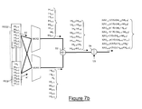
Figures 7a and7b schematically show the operation of the differentiating circuit comprised in the digital filter ofFigure 3 , when the length of the digital filter is L=3 and L=5, respectively. -
Figure 1 schematically shows a coherent optical receiver RX according to a preferred embodiment of the present invention. - The coherent optical receiver RX preferably comprises an analog portion AP, an in-phase analog-to-digital converter A/DI, a quadrature analog-to-digital converter A/DQ, a rotation compensator RC and a decision unit DU. The coherent optical receiver RX may comprise further modules, that are not shown in
Figure 1 and will not be described since they are not relevant to the present description. - The analog portion AP preferably has an input substantially corresponding to the input of the coherent optical receiver RX, and two outputs. The analog portion AP is preferably implemented as an arrangement of optical, electrical and electro-optical components. The physical implementation of the analog portion AP will not be described in detail, since it is not relevant to the present description.
- Preferably, the in-phase analog-to-digital converter A/DI and the quadrature analog-to-digital converter A/DQ are connected to the outputs of the analog portion AP. The outputs of the in-phase analog-to-digital converter A/DI and the quadrature analog-to-digital converter A/DQ are preferably connected to the inputs of the rotation compensator RC. The decision unit DU has two inputs, which are preferably connected to the outputs of the rotation compensator RC. The connections between outputs of the analog-to-digital converters A/DI, A/DQ and inputs of the rotation compensator RC are preferably implemented as parallel buses. Similarly, the connections between outputs of the rotation compensator RC and inputs of the decision unit DU are preferably implemented as parallel buses.
- When a modulated optical signal s(t)=A cos(2πft-θ) is received at the input of the optical coherent receiver RX, the analog portion AP preferably processes it for generating an in-phase component I' and a quadrature component Q' basically corresponding (except for noise and/or distortions introduced by propagation and/or by the analog portion AP itself) to the components I and Q of the modulated optical signal s(t). Both the in-phase component I' and the quadrature component Q' output by the analog portion AP are preferably in the form of analog electrical signals. The operation of the analog portion AP will not be described in further detail, since it is not relevant to the present description.
- Then, according to this first embodiment, the in-phase analog-to-digital converter A/DI preferably samples the in-phase component I', thereby generating a sequence of in-phase component samples I'k. Substantially at the same time, the quadrature analog-to-digital converter A/DQ preferably samples the quadrature component Q', thereby generating a sequence of quadrature component samples Q'k. Herein after, for simplicity, it is assumed that the sampling is performed at the symbol rate, so that each couple of samples (I'k, Q'k) correspond to a respective received symbol.
- As mentioned above, the couples of samples (I'k, Q'k) may be represented in the I-Q plane as points (I'k, Q'k) forming the received constellation, that is typically rotated relative to the reference constellation by a slowly varying rotation angle α.
- Preferably, the rotation compensator RC compensates such rotation according to the above mentioned known Viterbi and Viterbi algorithm, as it will be described in detail herein after, thereby providing at its output couples of compensated samples (I"k, Q"k). The couples of compensated samples (I"k, Q"k) may be represented in the I-Q plane as points (I"k, Q"k) forming a compensated received constellation, that advantageously overlap with the reference constellation (i.e. the "clouds" of the compensated received constellation are substantially centered around respective points of the reference constellation).
- Then, the rotation compensator RC preferably forwards the couples of compensated samples (I"k, Q"k) to the decision unit DU, that processes them for retrieving the digital data originally transmitted. The operation of the decision unit DU depends on the type of digital modulation applied to the modulated optical signal s(t), and will not be described in further detail, since it is not relevant to the present description.
- With reference to
Figure 2 , the rotation compensator RC according to a preferred embodiment of the present invention will be now described in detail. - The rotation compensator RC preferably comprises a first angle module ANGL1, a first multiplier M1, a first sine-cosine module SC1, a first digital filter Fx, a second digital filter Fy, a second angle module ANGL2, a second multiplier M2, an unwrapper UW, an adder S, a delay line D and a second sine-cosine module SC2.
- The first angle module ANGL1 preferably has two inputs corresponding to the inputs of the rotation compensator RC, and an output connected to the input of the first multiplier M1. The output of the first multiplier M1 is preferably connected to the input of the first sine-cosine module SC1. The first sine-cosine module SC1 preferably has two outputs, one connected to the input of the first digital filter Fx and the other connected to the input of the second digital filter Fy. The outputs of both the first digital filter Fx and second digital filter Fy are preferably connected to the input of the second angle module ANGL2. The output of the second angle module ANGL2 is preferably connected to the input of the second multiplier M2. The output of the second multiplier M2 is preferably connected to the input of the unwrapper UW. The input of the delay line D is preferably connected to the output of the first angle module ANGL1. The outputs of the delay line D and of the unwrapper UW are preferably connected to the inputs of the adder S. The output of the adder S is preferably connected to the input of the second sine-cosine module SC2. The second sine-cosine module SC2 has two outputs, that basically correspond to the outputs of the rotation compensator RC.
- The rotation compensator RC preferably comprises also a clock input suitable for receiving a clock signal from a clock unit (not shown in
Figure 1 ) comprised within the optical coherent receiver RX. - The operation of the rotation compensator RC according to a preferred embodiment of the present invention will be now described in detail.
- Preferably, at each clock cycle of the above mentioned clock signal, the rotation compensator RC preferably receives in parallel (i.e. substantially simultaneously) N couples of samples (I'k, Q'k), N being an integer equal to or higher than 2. For instance, N may be equal to 8, 16, 32, 64, 128, etc. The first sine-cosine module SC1 preferably converts the N couples of samples (I'k, Q'k) in N corresponding angular samples θ'k. Then, preferably, the first multiplier M1 multiplies each of the N angular samples θ'k by 2M, thereby bringing all the N angular samples θ'k into a same quadrant of the I-Q plane.
- Then, the first sine-cosine module SC1 preferably converts each of the N multiplied
angular samples 2M·θ'k into its respective real and imaginary components, thereby providing N real samples Xk=cos(2M·θ'k) and N imaginary samples Yk=sin (2M·θ'k). - The N real samples Xk=cos(2M·θ'k) are forwarded to the first digital filter Fx, that preferably calculates N real averages XAVk, each of the N real averages XAVk being calculated on a number L (L being equal to or higher than 3) of consecutive real samples, as it will be described in detail herein after. Substantially at the same time, the N imaginary samples Yk=sin(2M·θ'k) are forwarded to the second digital filter Fy, that preferably calculates N imaginary averages YAVk, each of the N imaginary averages YAVk being calculated on the same number L of consecutive imaginary samples, as it will be described in detail herein after.
- The N real averages XAVk and the N imaginary averages YAVk are then forwarded to the second angle module ANGL2, that preferably converts them in N corresponding angles. Then, the second multiplier M2 preferably divides such N corresponding angles by 2M, thereby providing N average angles θ'AVk. Then, preferably, the unwrapper UW compares each of the N average angles θ'AVk with the possible values θi of the phase θ for determining the closest one, and estimates N rotation angles αk as the difference between the average angle θ'AVk and the closest one among the possible values θi of the phase θ.
- Then, the adder S preferably receives the N angular samples θ'k (suitably delayed by the delay line D) and the N rotation angles αk, and calculates N compensated angular samples θ"k by subtracting from each angular samples θ'k the corresponding rotation angle αk. The N compensated angular samples θ"k are then forwarded to the second sine-cosine module SC2, that preferably converts each of the N compensated angular samples θ"k into its respective real and imaginary components, thereby providing N couples of compensated samples (I"k, Q"k), where I"k=cos(θ"k) are N compensated in-phase samples and Q"k=sin(θ"k) are N compensated quadrature samples.
- With reference to
Figure 3 , the first digital filter Fx will be now described in further detail. The second digital filter Fy substantially has the same structure and operation as the first digital filter Fx. Hence, a detailed description will be provided herein after only for the first digital filter Fx. For simplicity, the first digital filter Fx will be briefly termed in the following description "digital filter". - As mentioned above, at each clock cycle the digital filter Fx preferably receives N real samples Xk and provides at its output N real averages XAVk. according to the following operation (see above equation [2]):

- Accordingly, the digital filter Fx preferably has the following transfer function (see above equation [3]):

the multiplication by 1/L being omitted for simplicity. - The inventors have noticed that a known factorization may be applied to the transfer function of equation [3], thereby dividing it into a first transfer function:

and a second transfer function:
- Hence, the digital filter Fx may be implemented as a cascade of an integrating circuit having transfer function H1(z) and hence performing the following operation:


and a multiplier by 1/L performing the following operation:
- If the operation of equation [2] has to be performed not on the current sample and the L-1 preceding samples, but on the current sample, the (L-1)/2 preceding samples and the (L-1)/2 successive samples (i.e. the moving average should be centred on the current sample), equation [7] is:

and therefore equation [8] is:
-
Figure 3 schematically shows the structure of the digital filter Fx implemented substantially as a cascade of the above integrating circuit, the above differentiating circuit and a multiplier by 1/L. - More particularly, the digital filter Fx preferably comprises a cumulative sum module CS, a first addition module S1, a delay element D1, a first register REG1, a second register REG2, a first selector MUX1, a second selector MUX2, a second addition module S2 and a multiplication module Mx.
- The input of the cumulative sum module CS basically corresponds to the input of the digital filter Fx. The output of the cumulative sum module CS is preferably connected to one of the inputs of the first addition module S1. The output of the first addition module S1 is preferably connected to the input of the first register REG1. The first register REG1 has an output connected to the other input of the first addition module S1 via the delay element D1, according to a feedback configuration. Further, preferably, the first register REG1 is connected to the second register REG2. The outputs of the first and second registers REG1, REG2 are preferably connected to the inputs of the first and second selectors MUX1, MUX2, respectively. The outputs of the first and second selectors MUX1, MUX2 are preferably connected to the inputs of the second addition module S2. The input of the multiplication module Mx is preferably connected to the output of the second addition module S2. The output of the multiplication module Mx preferably corresponds to the output of the digital filter Fx. The bold lines in
Figure 3 preferably indicate parallel connections, i.e. connections capable of transporting N data in parallel. - When, at a given clock cycle, the digital filter Fx receives N samples Xk, Xk+1, ... Xk+N-1 from the first sine-cosine module SC1, the cumulative sum module CS preferably calculates N cumulative sums as follows:

- The cumulative sum module CS then preferably forwards the N cumulative sums Sk, Sk+1, ... Sk+N-1 to the first addition module S1. Substantially at the same time, the first addition module S1 receives from the delay element D1 a delayed integral Intk-1 that was calculated by the first addition module S1 on the N samples received at the previous clock cycle and that was stored in the first register REG1.
- The first addition module S1 then preferably adds the delayed integral Intk-1 to each of the N cumulative sums Sk, Sk+1, ... Sk+N-1, thereby providing at its output the following N integrals:

- The N integrals are then forwarded to the first register REG1, that preferably stores them, thereby overwriting N integrals Intk-N, Intk-N+1, ... Intk-1 calculated by the first addition module S1 on the N samples received at the previous clock cycle.
- It can be noticed that the cumulative sum module CS, the first addition module S1, the first register REG1 and the delay element D1 basically form an integrating circuit performing the integrating operation defined by the above equation [6]. In particular, the integrating operation is performed in two steps. Instead of calculating, for each sample Xk, Xk+1, ... Xk+N-1, the integral on all the previous samples (including the ones received during preceding clock cycles) as provided by equation [6], for each sample Xk, Xk+1, ... Xk+N-1 the cumulative sum block CS firstly calculates a "partial integral" (i.e. the cumulative sums Sk, Sk+1, ... Sk+N-1) only on the samples received during the current clock cycle. Afterwards, the first addition module S1 shifts all the partial integrals by a same amount (i.e. the delayed integral Intk-1) that basically is the integral calculated on all the samples received during the preceding clock cycles, i.e. received before the N currently received ones.
- This two-step implementation is advantageous, since the N integrals Intk, Intk+1, ... Intk+N-1 may be advantageously calculated in more than one clock cycle.
- Indeed, in principle the most straightforward solution for directly implementing the above operation [6] would be the circuit shown in
Figure 4 . For simplicity, it is assumed that N=8. The circuit comprises N=8 cascaded adders A0, A1, ... A7 and a delay block D forming a feedback loop between the first adder A0 and the last adder A7. At a first clock cycle, the circuit receives N=8 samples X0, X1, ... X7. The adder A0 provides Int0 equal to X0, and then the other adders A1, ... A7 operate in cascade for calculating the other integrals Int1, ... Int7 according to equation [6]. The last integral Int7 is then sent to the delay block D. At the next clock cycle, the circuit receives N=8 other samples X8, X9, ... X15 and the last integral Int7 from the delay block D. The first adder A0 sums X8 with Int7 for calculating I8, and then the other adders A1, ... A7 operate in cascade for calculating the other integrals Int9, ... Int15 according to equation [6]. In general, in the circuit ofFigure 4 , at each clock cycle N=8 new samples Xk, Xk+1, ... Xk+7 are received and, for calculating the corresponding N=8 integrals Intk, Intk+1, ... Intk+7, the integral Intk-1 must be available at the beginning of the current clock cycle. Similarly, for allowing proper operation of the circuit at the next clock cycle, the integral Intk+7 must be available at the beginning of the next clock cycle. In other words, all the integrals Intk, Intk+1, ... Intk+7 must be calculated in a single clock cycle. However, in an optical communication system a clock cycle is of few nanoseconds. Therefore, the cascaded operation of the N=8 adders should be completed within few nanoseconds. However, the current implementation of adders allows no more than 2-3 adders to operate in cascade in such a short time. The circuit ofFigure 4 is therefore not capable of calculating all the integrals Intk, Intk+1, ... Intk+7 in a single clock cycle. - The two-step implementation of the integrating operation defined by equation [6] advantageously removes the constraint of calculating the N integrals Intk, Intk+1, ... Intk+N-1 corresponding to the N currently received samples Xk, Xk+1, ... Xk+N-1 within the current clock cycle. Indeed, at each clock cycle, the cumulative sum module CS receives N samples Xk, Xk+1, ... Xk+N-1 and may start calculating the corresponding cumulative sums Sk, Sk+1, ...
S k+N1 without receiving any information derived from the N samples received during the previous clock cycle, because the cumulative sums Sk, Sk+1, ... Sk+N-1 are calculated only on the N currently received samples. The processing of the N samples received at the previous clock cycle may therefore still be running (i.e. the calculation of the N integrals corresponding to the N samples received at the previous clock cycle may be not completed yet), since none of these integrals is needed for starting calculation of the cumulative sums Sk, Sk+1, ... Sk+N-1. The only requirement is that the integral Intk-1 is available when the calculation of the cumulative sums Sk, Sk+1, ... Sk+N-1 by the cumulative sums block CS is finished, so that the first addition module S1 may add it to the cumulative sums Sk, Sk+1, ... Sk+N-1 for obtaining the integrals Intk, Intk+1, ... Intk+N-1. Therefore, advantageously, the calculation of the cumulative sums Sk, Sk+1, ... Sk+N-1 and therefore of the integrals Intk, Intk+1, ... Intk+N-1 may take more than one clock cycle. -
Figure 5 schematically shows the cumulative sum module CS according to a first variant of the present invention, in an exemplary case where N=8. - Similarly to the circuit of
Figure 4 , the cumulative sum module CS comprises N=8 cascaded adders A0, A1, ... A7. However, differently from the circuit ofFigure 4 , the cumulative sum module CS does not comprise any feedback loop between the first adder A0 and the last adder A7. At each clock cycle the cumulative sum module CS receives N=8 samples Xk, Xk+1, ... Xk+7. The first adder A0 preferably provides at the output of the cumulative sum module CS a first cumulative sum Sk=Xk. The other adders A1, ... A7 preferably then operate in cascade, thereby providing the other cumulative sums Sk+1, ... Sk+7. - The whole operation may advantageously take multiple clock cycles. For instance, assuming that each adder performs a sum in a clock cycle, during a first clock cycle N=8 samples Xk, Xk+1, ... Xk+7 are received, and the first adder A0 calculates the cumulative sum Sk=xk. During a second clock cycle, the second adder A1 calculates the cumulative sum Sk+1=xk+xk+1, while N=8 further samples Xk+8, Xk+9, ... Xk+15 are received and the first adder A0 calculates the cumulative sum Sk+8=xk+8. During a third clock cycle, the third adder A2 calculates the cumulative sum Sk+2=xk+xk+1+xk+2, the second adder A1 calculates the cumulative sum Sk+9=xk+8+xk+9, while N=8 further samples Xk+16, Xk+17, ... Xk+23 are received and the first adder A0 calculates the cumulative sum Sk+16=xk+16. And so on. At the eighth clock cycle, the last adder A7 calculates the cumulative sum Sk+7= Xk+ Xk+1+ ... Xk+N-1. The cumulative sums Sk, Sk+1, Sk+2, ..., Sk+7 calculated on the N=8 samples Xk, Xk+1, ... Xk+7 received at the first clock cycle are then finally output in parallel by the cumulative sum module CS, while the processing of the N=8 samples received at the second, third, .... eight clock cycle is still in progress.
- For implementing the above described cascaded operation (in particular, for synchronizing the inputs and outputs of the adders), the cumulative sum module CS preferably comprises a number of delay blocks d suitably distributed at the inputs of the adders A0, A1, ..., A7, at the output of the adders A0, A1, ... A7 and between each couple of consecutive adders A0, A1, ... A7, as schematically shown in
Figure 5 . - In particular, if N is the number of samples received at each clock cycle (and therefore N is the number of cascaded adders comprised in the cumulative sum module CS), assuming that each adder performs a sum in a clock cycle and that each delay block d introduces a delay of a single clock cycle, the overall number of delay blocks d preferably is N2-1. In the exemplary case shown in
Figure 5 , where N=8, the overall number of delay blocks d is (82-1 )=63. More generally, if a number R (R<N) of the N adders can operate in cascade within a single clock cycle, a single delay block d is needed at the output of the cascade of R adders. Then, the overall number of delay blocks d preferably is about equal to N2/R. In any case, the complexity of the cumulative sum module CS shown inFigure 5 increases substantially proportionally to N2. -
Figure 6 schematically shows the cumulative sum module according to a second variant of the present invention, in an exemplary case where N=8. - According to this second variant, a cumulative sum module CS(N) suitable for receiving N samples in parallel preferably comprises N/2 input adders, (N/2)-1 output adders and a nested cumulative sum module CS(N/2) interposed between the N/2 input adders and the (N/2)-1 output adders. Similarly, the nested cumulative sum module CS(N/2) preferably comprises N/4 input adders, (N/4)-1 output adders and a nested cumulative sum module CS(N/4) interposed between the N/4 input adders and the (N/4)-1 output adders. And so on. The cumulative sum module CS(N) preferably comprises log2(N)-1 cumulative sum modules nested one in the other. The innermost cumulative sum module CS(2) preferably comprises a single adder.
-
Figure 6 shows a cumulative sum module according to the second variant, where N=8 by way of example. Hence, the cumulative sum module CS(8) comprises 4 input adders Ai80, Ai81, Ai82, Ai83, 3 output adders Ao80, Ao81, Ao82 and a nested cumulative sum module CS(4). The cumulative sum module CS(4) preferably comprises 2 input adders Ai40 and Ai41, 1 output adder Ao40 and a nested cumulative sum module CS(2), that is also the innermost one. The cumulative sum module CS(2) preferably comprises a single adder A20. - According to this second variant, the cumulative sum module CS(N) has N inputs and N outputs, the cumulative sum module CS(N/2) has N/2 inputs and N/2 outputs, and so on. The innermost cumulative sum module CS(2) preferably has 2 inputs and 2 outputs.
- The N inputs of the N/2 input adders of the cumulative sum module CS(N) basically correspond to the N inputs of the cumulative sum module CS(N), while the N/2 outputs of the N/2 input adders of the cumulative sum module CS(N) are connected to the N/2 inputs of the cumulative sum module CS(N/2). Similarly, the N/2 inputs of the N/4 input adders of the cumulative sum module CS(N/2) basically correspond to the N/2 inputs of the cumulative sum module CS(N/2), while the N/4 outputs of the N/4 input adders of the cumulative sum module CS(N/2) are connected to the N/4 inputs of the cumulative sum module CS(N/4). And so on.
- Therefore, with reference to
Figure 6 (exemplary case with N=8), the cumulative sum module CS(8) has 8 inputs and 8 outputs, the cumulative sum module CS(4) has 4 inputs and 4 outputs, and the innermost cumulative sum module CS(2) has 2 inputs and 2 outputs. All the inputs and outputs are represented inFigure 6 as squares. Preferably, the 8 inputs of the 4 input adders Ai80, Ai81, Ai82, Ai83 basically correspond to the 4 inputs of the cumulative sum module CS(8), while the 4 outputs of the 4 input adders Ai80, Ai81, Ai82, Ai83 are connected to the 4 inputs of the cumulative sum module CS(4). Similarly, the 4 inputs of the 2 input adders Ai40, Ai41 basically correspond to the 4 inputs of the cumulative sum module CS(4), while the 2 outputs of the 2 input adders Ai40, Ai41 are connected to the 2 inputs of the cumulative sum module CS(2). - According to this second variant, the even inputs of the cumulative sum module CS(N) preferably bypass all the nested cumulative sum modules. In particular, the first input of the cumulative sum module CS(N) is preferably connected to the first output of the cumulative sum module CS(N), while each of the other (N/2)-1 even inputs of the cumulative sum module CS(N) is connected to an input of a respective one of the (N/2)-1 output adders of the cumulative sum module CS(N). The other input of the (N/2)-1 output adders of the cumulative sum module CS(N) is preferably connected to (N/2)-1 of the N/2 outputs of the cumulative sum module CS(N/2) (except the last one). Similarly, the even inputs of the cumulative sum module CS(N/2) preferably bypass all the nested cumulative sum modules. In particular, the first input of the cumulative sum module CS(N/2) is preferably connected to the first output of the cumulative sum module CS(N/2), while each of the other (N/4)-1 even inputs of the cumulative sum module CS(N/2) is connected to an input of a respective one of the (N/4)-1 output adders of the cumulative sum module CS(N/2). The other input of the (N/4)-1 output adders of the cumulative sum module CS(N/2) is preferably connected to (N/4)-1 of the N/4 outputs of the cumulative sum module CS(N/4) (except the last one). And so on.
- Therefore, with reference to
Figure 6 (exemplary case with N=8), the even inputs of the cumulative sum module CS(8) preferably bypass the inner cumulative sum modules CS(4) and CS(2). In particular, the first input of the cumulative sum module CS(8) is preferably connected to the first output of the cumulative sum module CS(8), while each of the other 3 even inputs of the cumulative sum module CS(8) is connected to an input of a respective one of the output adders Ao80, Ao81, Ao82. The other input of the output adders Ao80, Ao81, Ao82 is preferably connected to 3 of the 4 outputs of the cumulative sum module CS(4) (except the last one). Similarly, the even inputs of the cumulative sum module CS(4) preferably bypass the inner cumulative sum module CS(2). In particular, the first input of the cumulative sum module CS(4) is preferably connected to the first output of the cumulative sum module CS(4), while the other even input of the cumulative sum module CS(4) is connected to an input of the output adder Ao40. The other input of the output adder Ao40 is preferably connected to one of the 2 outputs of the cumulative sum module CS(2) (not the last one). - When at a clock cycle N=8 samples Xk, Xk+1, ... Xk+7 are received at the cumulative sum module CS(8), the input adders Ai80, Ai81, Ai82, Ai83 preferably add them two-by-two thereby providing the 4 following sums:


to the cumulative sum module CS(4). At the same time, the even samples Xk, Xk+2, Xk+4 and Xk+6 preferably bypass the cumulative sum modules C(4) and C(2). In particular, the first even sample Xk is directly forwarded at the first output of the cumulative sum module CS(8), while the other even samples Xk+2, Xk+4 and Xk+6 are preferably provided at one of the inputs of the output adders Ao80, Ao81, Ao82, respectively. - Then, in the cumulative sum module CS(4), the input adders Ai40, Ai41 preferably add the sums Si80, Si81, Si82, Si83 two-by-two, thereby providing the 2 following sums:


- to the cumulative sum module CS(2). At the same time, the even sums Si80 and Si82 preferably bypass the cumulative sum module C(2). In particular, the first even sum Si80 is directly forwarded at the first output of the cumulative sum module CS(4), while the other even sum Si82 is preferably provided at one of the inputs of the output adder Ao40.
- Then, in the cumulative sum module CS(2), the adder A20 preferably adds the sums Si40 and Si41, thereby providing the followings sum:

at its output. At the same time, also the sum Si40 is forwarded at the first output of the cumulative sum module CS(2). - Preferably, the first sample Xk, the sum Si80, the sum Si40 and the sum S20 are directly forwarded at the output of the cumulative sum module C(8), since they correspond to the cumulative sums Sk, Sk+1, Sk+3 and Sk+7, respectively.
- Then, in the cumulative sum module CS(4), the output adder Ao40 preferably adds Si40 with Si82, thereby providing the followings sum:

- The sum So40 corresponds to the cumulative sum Sk+5, and is therefore directly forwarded at the output of the cumulative sum module C(8).
- Then, in the cumulative sum module CS(8), the output adders Ao80, Ao81 and Ao82 preferably add Si80, Si40 and So40 to the even samples Xk+2, Xk+4 and Xk+6, respectively, thereby providing the followings sums:


- The sums So80, So81 and So82 corresponds to the cumulative sums Sk+2, Sk+4 and Sk+6, respectively, and are therefore directly forwarded at the output of the cumulative sum module C(8).
- By comparing the cumulative sum module of
Figure 5 with the cumulative sum module ofFigure 6 , it can be noticed that the latter comprises a higher number of adders. Indeed, while the cumulative sum module ofFigure 5 comprises N adders, the cumulative sum module ofFigure 6 comprises 2N-log2(N)-2 adders. However, the maximum number of adders operating in cascade is advantageously reduced. Indeed, while in the configuration ofFigure 5 all the N adders are cascaded, in the configuration ofFigure 6 no more than 2log2(N)-2 adders are cascaded (the cascade comprising the maximum number of adders is the one providing the cumulative sum Sk+6 or, more generally, the cumulative sum Sk+N-2). In other words, the configuration ofFigure 6 has a higher parallelism degree than the configuration ofFigure 5 . As a consequence, a reduced number of delay blocks d is advantageously required for synchronizing inputs and outputs of the various adders. The delay blocks d are not shown inFigure 6 for not overloading the Figure. In particular, if N is the number of samples received at each clock cycle, assuming that each adder performs a sum in a clock cycle and that each delay block d introduces a delay of a single clock cycle, the overall number of delay blocks d preferably is N x (2log2(N)-2). If 3-4 adders may operate in cascade within a single clock cycle, only two "vertical strips" each comprising N delay blocks d are needed. In this case, only 2N delay blocks d are needed. Therefore, the complexity of the cumulative sum module CS shown inFigure 6 increases substantially proportionally to N·log2(N). The configuration ofFigure 6 is therefore advantageously much simpler (and therefore much cheaper) than the configuration ofFigure 5 since, for a same value of N, it comprises a much lower number of components. - Referring again to
Figure 3 , while the first register REG1 receives the N integrals Intk, Intk+1, ... Intk+N-1 from the first addition module S1 and stores them, it preferably forwards the N integrals Intk-N, Intk-N+1, ...., Intk-1 previously stored therein to the second register REG2. The ensemble of the two registers REG1 and REG2 therefore advantageously provides a "window" of 2N integrals. - Then, the first selector MUX1 preferably selects from the first register REG1 and the second register REG2 N integrals, and provides them in parallel at its outputs. In particular, the first selector MUX1 preferably selects from the first register REG1 the last (N/2)-((L-1)/2) integrals and from the first register REG1 the first (N/2)+((L-1)/2) integrals. The N integrals selected by the first selector MUX1 are therefore:


- Substantially at the same time, also the second selector MUX2 preferably selects from the first register REG1 and the second register REG2 N integrals, and provides them in parallel at its outputs. In particular, the second selector MUX2 preferably selects from the first register REG1 the last (N/2)+((L-1)/2) integrals and from the first register REG1 the first (N/2)-((L-1)/2) integrals. The N integrals selected by the second selector MUX2 are therefore:


- Hence, for allowing proper operation of the first and second selectors MUX1, MUX2, L should be lower than N.
- It can be noticed the integrals output by the first selector MUX1 and the second selector MUX2 are offset by L-1. For instance,
Figure 7a and7b schematically show the operation of the registers REG1, REG2 and the selectors MUX1, MUX2 in case L=3 (Figure 7a ) and in case L=5 (Figure 7b ), in the exemplary situation where N=8. In both cases, the first register REG1 stores N=8 integrals Intk, Intk+1, ... Intk+7 calculated at a clock cycle, while the second register REG2 stores N=8 integrals Intk-8, Intk-7, ... Intk-1, calculated at the previous clock cycle. - With reference first to
Figure 7a (L=3), the first selector MUX1 preferably selects from the first register REG1 and the second register REG2 the N=8 integrals Intk-3, Intk-2, ..., Intk+4 (as indicated by the arrow A1), while the second selector MUX2 preferably selects from the first register REG1 and the second register REG2 the N=8 integrals Intk-5, Intk-4, ..., Intk+2 (as indicated by the arrow A2). The integrals output by the first selector MUX1 and the second selector MUX2 in this first case are offset by L-1 =2. - With reference now to
Figure 7b (L=5), the first selector MUX1 preferably selects from the first register REG1 and the second register REG2 the N=8 integrals Intk-2, Intk-1, ..., Intk+5 (as indicated by the arrow A1), while the second selector MUX2 preferably selects from the first register REG1 and the second register REG2 the N=8 integrals Intk-6, Intk-5, ..., Intk+1 (as indicated by the arrow A2). The integrals output by the first selector MUX1 and the second selector MUX2 in this first case are offset by L-1 =4. - The integrals output by the first selector MUX1 and the integrals output by the second selector MUX2 are then preferably forwarded to the second addition module S2, that preferably calculates N differences according to the above equation [7'], i.e.:


- It can be noticed that each of the above differences basically is a difference between the integral output by the first selector MUX1 corresponding to the sample which follows the current sample by (L-1)/2 and the integral output by the second selector MUX2 which corresponds to the sample that precedes the current sample by (L-1)/2, in accordance with equation [7'].
- Therefore, by referring again to
Figure 7a (N=8, L=3), the second addition module S2 preferably calculates N=8 differences as follows:


- Similarly, by referring again to
Figure 7b (N=8, L=5), the second addition module S2 preferably calculates the N=8 differences as follows:


- The N differences are then forwarded to the multiplication module Mx, that preferably multiples each of the N differences by 1/L, thereby providing at its output the following N real averages XAVk-(N/2), ..., XAVk+(N/2)-1 according to the above equation [8']:


- Therefore, by referring again to
Figure 7a (N=8, L=3), the multiplication module Mx preferably calculates N=8 real averages as follows:


- Similarly, by referring again to
Figure 7b (N=8, L=5), the multiplication module Mx preferably calculates the N=8 real averages as follows:


- The N real averages XAVk-(N/2), ..., XAVk+(N/2)-1 are then provided at the output of the digital filter Fx. Since, as mentioned above, the operation of the digital filter Fy is basically the same as the operation of the digital filter Fx, in the meanwhile also the second digital filter Fy outputs N imaginary averages YAVk-(N/2), ..., YAVk+(N/2)-1. The N real and imaginary averages are then received by the second angle module ANGL2, that processes them as described above.
- It can be noticed that the N real averages XAVk-(N/2), ..., XAVk+(N/2)-1 output by the filters Fx (and therefore the corresponding imaginary averages output by the filter Fy) are delayed by N/2 relative to the N real samples Xk, Xk+1, ... Xk+N-1 entering the filter Fx (and therefore the corresponding imaginary samples entering the filter Fy). Therefore, also the N rotation angles αk calculated by the unwrap module UW based on the N real averages XAVk-(N/2), ..., XAVk+(N/2)-1 (and the corresponding imaginary averages) are delayed by N/2 relative to the N angular samples θ'k output by the first angle module ANGL1. This delay is advantageously compensated by the delay line D.
- Therefore, the ensemble of the two registers REG1, REG2, the two selectors MUX1, MUX2 and the second addition module S2 basically forms a differentiating circuit performing the differentiating operation defined by the above equation [7'].
- Advantageously, the length of the filter Fx may be changed by changing L. This operation advantageously does not affect the operation of the integrating circuit, and may be simply implemented by suitably shifting the inputs of the selectors MUX1, MUX2. For instance, with reference to
Figures 7a and7b , increasing the length of the digital filter Fx from L=3 (Figure 7a ) to L=5 (Figure 7b ) simply requires shifting forward the inputs of the first selector MUX1 by a single position, and shifting backward the inputs of the second selector MUX2 by a single position. Generally speaking, varying the length of the digital filter Fx from a first value L1 to a second value L2 (for instance, when noise conditions change or when one wishes testing the performance of the receiver RX) requires shifting forward the inputs of the first selector MUX1 by (L2-L1)/2 positions, and shifting backward the inputs of the second selector MUX2 by (L2-L1)/2 positions. - Advantageously, this shifting is always symmetric relative to the center of the concatenation of the first and second registers REG1, REG2. Therefore, advantageously, changing the length of the digital filter Fx is hitless (i.e. it does not induce any loss of data), since it does not affect the delay between the N input real samples Xk, Xk+1, ... Xk+N-1 and the N output real averages XAVk-(N/2), ..., XAVk+(N/2)-1. This delay is advantageously constantly equal to N/2, and is therefore compensated by the delay line D independently of the value of L.
- In the above description, the digital filter Fx is part of a rotation compensator for an optical coherent receiver. This is however non limiting, since the digital filter Fx may be used in other digital devices suitable for processing digital samples. In particular, the digital filter Fx may be advantageously used each time a moving sum of L consecutive digital samples has to be performed on a sequence of digital samples received at a digital device having a parallelism degree equal to N. The use of the digital filter Fx for calculating a moving average in a rotation compensator for an optical coherent receiver is therefore merely exemplary.
- The functions of the various elements shown in
Figure 3 may be provided through the use of dedicated hardware, programmable hardware or a hardware capable of executing software in association with appropriate software. In particular, the functions of the various elements shown inFigure 3 are preferably provided through the use of one or more application specific integrated circuits (ASIC) and/or one or more field programmable gate arrays (FPGA). Preferably, the functions of the various elements shown inFigure 3 are provided through the use of a single ASIC or a single FPGA. Therefore, the expressions "integrating circuit" and "differentiating circuit" mentioned in the claims are to be understood merely as functional aggregations of the elements of the digital filter, and they should not be understood necessarily as physically separated circuits implemented on separated hardware devices.
Claims (15)
- A digital filter (Fx) configured to receive a sequence of digital samples, said digital filter (Fx) being configured to receive in parallel N digital samples (Xk) of said sequence at each clock cycle of a clock signal suitable for synchronizing operation of said digital filter (Fx), N being an integer higher than 1, and to calculate a sum (XAVk) of L consecutive digital samples of said sequence, L being an odd integer equal to or higher than 3 and lower than N, said digital filter (Fx) comprising:- an integrating circuit (CS, S1, REG1, D) configured to calculate a first integral (Intk-((L-1)/2)) of said sequence up to a first digital sample (Xk-((L-1)/2)) of said L consecutive digital samples and a last integral (Intk+((L-1)/2)) of said sequence up to a last digital sample (Xk+((L-1)/2)) of said L consecutive digital samples; and- a differentiating circuit (REG1, REG2, MUX1, MUX2, S2) configured to calculate said sum (XAVk) as a difference between said last integral (Intk+((L-1)/2)) and said first integral (Intk-((L-1)/2)),wherein said integrating circuit (CS, S1, REG1, D) comprises a cumulative sum module (CS), an addition module (S1) connected to said cumulative sum module (CS) and a first register (REG1) retroactively connected to said addition module (S1), wherein:- said cumulative sum module (CS) is configured to calculate a last cumulative sum (Sk+((L-1)/2)) of said last digital sample (Xk+((L-1)/2)) and preceding digital samples of said sequence received within a same clock cycle as said last digital sample (Xk+((L-1)/2));- said first register (REG1) is configured to store a delayed integral (Intk-1) calculated on digital samples of said sequence received before said same clock cycle; and- said addition module (S1) is configured to calculate said last integral (Intk+((L-1)/2)) by adding said last cumulative sum (Sk+((L-1)/2)) and said delayed integral (Intk-1).
- The digital filter (Fx) according to claim 1, wherein said cumulative sum module (CS) is configured to receive in parallel N digital samples (Xk, Xk+1, ... Xk+N-1) of said sequence of digital samples in said same clock cycle, and to provide N cumulative sums (Sk, Sk+1, ... Sk+N-1) in parallel, said N cumulative sums (Sk, Sk+1, ... Sk+N-1) including said last cumulative sum (Sk+((L-1)/2)).
- The digital filter (Fx) according to claim 2, wherein said addition module (S1) is configured to receive in parallel said N cumulative sums (Sk, Sk+1, ... Sk+N-1) and to add said delayed integral (Intk-1) to each of said N cumulative sums (Sk, Sk+1, ... Sk+N-1), thereby providing in parallel N currently calculated integrals (Intk, Intk+1, ... Intk+N-1), said N currently calculated integrals (Intk, Intk+1, ... Intk+N-1) including said last integral (Intk+((L-1)/2)).
- The digital filter (Fx) according to claim 3, wherein said first register (REG1) is configured to:- before receiving said N currently calculated integrals (Intk, Intk+1, ... Intk+N-1), storing N previously calculated integrals (Intk-N, Intk-N+1, ... Intk-1), said N previously calculated integrals (Intk-N, Intk-N+1, ... Intk-1) including said delayed integral (Intk-1) and said first integral (Intk-((L-1)/2)); and- receive from said addition module (S1) said N currently calculated integrals (Intk, Intk+1, ... Intk+N-1) and store them, thereby overwriting said N previously calculated integrals (Intk-N, Intk-N+1, ... Intk-1).
- The digital filter (Fx) according to claim 4, wherein said differentiating circuit (REG1, REG2, MUX1, MUX2, S2) comprises a second register (REG2) cooperating with said first register (REG1), and wherein said first register (REG1) is configured to, upon reception of said N currently calculated integrals (Intk, Intk+1, ... Intk+N-1), forward said N previously calculated integrals (Intk-N, Intk-N+1, ... Intk-1) to said second register (REG2), before overwriting them.
- The digital filter (Fx) according to claim 5, wherein said differentiating circuit (REG1, REG2, MUX1, MUX2, S2) further comprises a first selector (MUX1) and a second selector (MUX2) connected to said first register (REG1) and said second register (REG2), and wherein:- said first selector (MUX1) is configured to read from said first register (REG1) and said second register (REG2) N minuend integrals (Intk-(N/2)+((L-1)/2), ... Intk+(N/2)-1+((L-1)/2)) selected among said N previously calculated integrals (Intk-N, Intk-N+1, ... Intk-1) and said N currently calculated integrals (Intk, Intk+1, ... Intk+N-1), said N minuend integrals (Intk-(N/2)+((L-1)/2), ... Intk+(N/2)-1+((L-1)/2)) including said last integral (Intk+((L-1)/2)); and- said second selector (MUX2) is configured to read from said first register (REG1) and said second register (REG2) N subtrahend integrals (Intk-(N/2)-((L-1)/2), ... Intk+(N/2)-1-((L-1)/2)) selected among said N previously calculated integrals (Intk-N, Intk-N+1, ... Intk-1) and said N currently calculated integrals (Intk, Intk+1, ... Intk+N-1), said N subtrahend integrals (Intk-(N/2)-((L-1)/2), ... Intk+(N/2)-1-((L-1)/2)) including said first integral (Intk-((L-1)/2)), wherein said N minuend integrals (Intk-(N/2)+((L-1)/2), ... Intk+(N/2)-1+((L-1)/2)) are shifted by L-1 relative to said N subtrahend integrals (Intk-(N/2)-((L-1)/2), ... Intk+(N/2)-1-((L-1)/2)).
- The digital filter (Fx) according to claim 6, wherein:- said N minuend integrals (Intk-(N/2)+((L-i)/2), ... Intk+(N/2)-1+((L-1)/2)) are a concatenation of the last (N/2)-((L-1)/2) integrals of said N previously calculated integrals (Intk-N, Intk-N+1, ... Intk-1) and the first (N/2)+((L-1)/2) integrals of said N currently calculated integrals (Intk, Intk+1, ... Intk+N-1); and- said N subtrahend integrals (Intk-(N/2)-((L-1)/2), ... Intk+(N/2)-1-((L-1)/2)) are a concatenation of the last (N/2)+((L-1)/2) integrals of said N previously calculated integrals (Intk-N, Intk-N+1, ... Intk-1) and the first (N/2)-((L-1)/2) integrals of said N currently calculated integrals (Intk, Intk+1, ... Intk+N-1).
- The digital filter (Fx) according to claim 6 or 7, wherein said differentiating circuit (REG1, REG2, MUX1, MUX2, S2) further comprises a second addition module (S2) connected to said first selector (MUX1) and said second selector (MUX2), said second addition module (S2) being configured to calculate N differences between said N minuend integrals (Intk-(N/2)+((L-1)/2), ... Intk+(N/2)-1+((L-1)/2)) and said N subtrahend integrals (Intk-(N/2)-((L-1)/2), ... Intk+(N/2)-1-((L-1)/2)), said N differences including said difference between said last integral (Intk+((L-1)/2)) and said first integral (Intk-((L-1)/2)).
- The digital filter (Fx) according to any of the preceding claims, wherein said cumulative sum module (CS(8)) comprises log2(N)-1 further cumulative sum modules (SC(4), CS(2)) nested one in the other.
- The digital filter (Fx) according to claim 9, wherein:- said cumulative sum module (CS(8)) comprises N/2 input adders (Ai80, Ai81, Ai82, Ai83), (N/2)-1 output adders (Ao80, Ao81, Ao82) and a first further cumulative sum module (CS(4)) interposed between said N/2 input adders (Ai80, Ai81, Ai82, Ai83) and said (N/2)-1 output adders (Ao80, Ao81, Ao82); and- said first further cumulative sum module (CS(4)) comprises N/4 first further input adders (Ai40, Ai41), (N/4)-1 first further output adders (Ao40) and a second further cumulative sum module (CS(2)) interposed between said N/4 first further input adders (Ai40, Ai41) and said (N/4)-1 first further output adders (Ao40).
- The digital filter (Fx) according to claim 9 or 10, wherein said further cumulative sum modules (SC(4), CS(2)) include an innermost further cumulative sum module (CS(2)) in turn comprising a single adder.
- The digital filter (Fx) according to any of claims 1 to 8, wherein said cumulative sum module (CS) comprises N cascaded adders.
- A rotation compensator (RC) for an optical coherent receiver (RX) configured to receive a modulated optical signal (s(t)), process said modulated optical signal (s(t)) for generating an in-phase component (I') and a quadrature component (Q'), and sample said in-phase component (I') and said quadrature component (Q') for generating couples of samples (I'k, Q'k) of said in-phase component (I') and said quadrature component (Q'), said couples of samples (I'k, Q'k) forming a received constellation that is rotated relative to a reference constellation by a rotation angle, said rotation compensator (RC) comprising:- a first angle module (ANGL1) configured to receive in parallel N couples of samples (I'k, Q'k) and to convert them in N corresponding angular samples (θ'k);- an estimating circuit (M1, SC1, Fx, Fy, ANGL2, M2, UW) configured to process said N corresponding angular samples (θ'k) for estimating N rotation angles (αk);- a compensating circuit (D, S) configured to apply said N rotation angles (αk) to said N corresponding angular samples (θ'k), thereby providing N compensated angular samples (θ"k); and- a first sine-cosine module (SC2) configured to receive said N compensated angular samples (θ"k) in parallel and to convert them in N corresponding couples of compensated samples (I"k, Q"k),wherein said estimating circuit (M1, SC1, Fx, Fy, ANGL2, M2, UW) comprises a digital filter (Fx, Fy) according to any of the preceding claims.
- A coherent optical receiver (RX) for an optical communication network configured to receive a modulated optical signal (s(t)) and to process said modulated optical signal (s(t)) for generating an in-phase component (I') and a quadrature component (Q'), said coherent optical receiver (RX) comprising a rotation compensator (RC) according to claim 13.
- An optical communication network comprising an optical coherent receiver (RX) according to claim 14.
Priority Applications (2)
| Application Number | Priority Date | Filing Date | Title |
|---|---|---|---|
| ES10305420.1T ES2614611T3 (en) | 2010-04-21 | 2010-04-21 | Parallel digital filter |
| EP10305420.1A EP2381596B1 (en) | 2010-04-21 | 2010-04-21 | Parallel digital filter |
Applications Claiming Priority (1)
| Application Number | Priority Date | Filing Date | Title |
|---|---|---|---|
| EP10305420.1A EP2381596B1 (en) | 2010-04-21 | 2010-04-21 | Parallel digital filter |
Publications (2)
| Publication Number | Publication Date |
|---|---|
| EP2381596A1 true EP2381596A1 (en) | 2011-10-26 |
| EP2381596B1 EP2381596B1 (en) | 2016-11-09 |
Family
ID=42752073
Family Applications (1)
| Application Number | Title | Priority Date | Filing Date |
|---|---|---|---|
| EP10305420.1A Not-in-force EP2381596B1 (en) | 2010-04-21 | 2010-04-21 | Parallel digital filter |
Country Status (2)
| Country | Link |
|---|---|
| EP (1) | EP2381596B1 (en) |
| ES (1) | ES2614611T3 (en) |
Citations (3)
| Publication number | Priority date | Publication date | Assignee | Title |
|---|---|---|---|---|
| US4558454A (en) * | 1983-04-11 | 1985-12-10 | National Information Utilities Corporation | Digital partial response filter |
| FR2785747A1 (en) * | 1998-11-09 | 2000-05-12 | Commissariat Energie Atomique | DIGITAL FILTER WITH PARALLEL ARCHITECTURE AND SIGNAL RECEIVER WITH SPRAY OF SPECTRUM USING SUCH A FILTER |
| US6636570B1 (en) * | 1999-06-21 | 2003-10-21 | Hyundai Electronics Industries Co., Ltd. | Phase detection apparatus for compensating phase rotation error |
-
2010
- 2010-04-21 EP EP10305420.1A patent/EP2381596B1/en not_active Not-in-force
- 2010-04-21 ES ES10305420.1T patent/ES2614611T3/en active Active
Patent Citations (3)
| Publication number | Priority date | Publication date | Assignee | Title |
|---|---|---|---|---|
| US4558454A (en) * | 1983-04-11 | 1985-12-10 | National Information Utilities Corporation | Digital partial response filter |
| FR2785747A1 (en) * | 1998-11-09 | 2000-05-12 | Commissariat Energie Atomique | DIGITAL FILTER WITH PARALLEL ARCHITECTURE AND SIGNAL RECEIVER WITH SPRAY OF SPECTRUM USING SUCH A FILTER |
| US6636570B1 (en) * | 1999-06-21 | 2003-10-21 | Hyundai Electronics Industries Co., Ltd. | Phase detection apparatus for compensating phase rotation error |
Non-Patent Citations (1)
| Title |
|---|
| SEB J SAVORY: "Digital filters for coherent optical receivers", OPTICS EXPRESS, OSA (OPTICAL SOCIETY OF AMERICA), WASHINGTON DC, (US) LNKD- DOI:10.1364/OE.16.000804, vol. 16, no. 2, 21 January 2008 (2008-01-21), pages 804 - 817, XP007906766, ISSN: 1094-4087 * |
Also Published As
| Publication number | Publication date |
|---|---|
| ES2614611T3 (en) | 2017-06-01 |
| EP2381596B1 (en) | 2016-11-09 |
Similar Documents
| Publication | Publication Date | Title |
|---|---|---|
| US5757862A (en) | Demodulator, modulation and demodulation system, and demodulation method | |
| US5832043A (en) | System and method for maintaining continuous phase during up/down conversion of near-zero hertz intermediate frequencies | |
| EP0772330A2 (en) | Receiver and method for receiving OFDM signals | |
| US20020122505A1 (en) | Frequency and phase estimation for MPSK signals | |
| EP0771097B1 (en) | Differential detecting apparatus for PSK signals | |
| US3991377A (en) | Differential phase shift keying demodulator | |
| EP1388942B1 (en) | Conversion circuit, tuner and demodulator | |
| JP3399400B2 (en) | Frequency shift demodulation circuit | |
| EP2381596B1 (en) | Parallel digital filter | |
| CN115632923B (en) | OQPSK-based unmanned aerial vehicle and satellite ultra-wideband communication method and related equipment | |
| CN100546294C (en) | Time extraction device and method, and demodulation device including the time extraction device | |
| US6504879B1 (en) | Digital modulation apparatus | |
| EP2995052B1 (en) | Correction of quadrature phase and gain mismatch in receiver down-conversion using a dual cordic architecture | |
| KR100959229B1 (en) | Data receiver | |
| CN100514951C (en) | Apparatus and method for digital modulation | |
| JP4214635B2 (en) | Digital radio equipment | |
| JPH06237277A (en) | Psk carrier signal regenerating device | |
| EP2976852B1 (en) | Timing recovery apparatus | |
| JP3129947B2 (en) | Digital quadrature detector | |
| KR100192798B1 (en) | A matched filter of quadrature phase shift keying demodulator | |
| JP2943803B1 (en) | Receiver | |
| JPH0583314A (en) | Demodulation circuit | |
| JP4632929B2 (en) | Demodulator | |
| JP2014143656A (en) | Optical receiving device | |
| JP2002118495A (en) | Spread spectrum communication correlator |
Legal Events
| Date | Code | Title | Description |
|---|---|---|---|
| 17P | Request for examination filed |
Effective date: 20101115 |
|
| AK | Designated contracting states |
Kind code of ref document: A1 Designated state(s): AT BE BG CH CY CZ DE DK EE ES FI FR GB GR HR HU IE IS IT LI LT LU LV MC MK MT NL NO PL PT RO SE SI SK SM TR |
|
| AX | Request for extension of the european patent |
Extension state: AL BA ME RS |
|
| PUAI | Public reference made under article 153(3) epc to a published international application that has entered the european phase |
Free format text: ORIGINAL CODE: 0009012 |
|
| RAP1 | Party data changed (applicant data changed or rights of an application transferred) |
Owner name: ALCATEL LUCENT |
|
| 111Z | Information provided on other rights and legal means of execution |
Free format text: AT BE BG CH CY CZ DE DK EE ES FI FR GB GR HR HU IE IS IT LI LT LU LV MC MK MT NL NO PL PT RO SE SI SK SM TR Effective date: 20130410 |
|
| RAP1 | Party data changed (applicant data changed or rights of an application transferred) |
Owner name: ALCATEL LUCENT |
|
| D11X | Information provided on other rights and legal means of execution (deleted) | ||
| REG | Reference to a national code |
Ref country code: DE Ref legal event code: R079 Ref document number: 602010037802 Country of ref document: DE Free format text: PREVIOUS MAIN CLASS: H04B0010148000 Ipc: H04B0010610000 |
|
| GRAP | Despatch of communication of intention to grant a patent |
Free format text: ORIGINAL CODE: EPIDOSNIGR1 |
|
| INTG | Intention to grant announced |
Effective date: 20160707 |
|
| RIC1 | Information provided on ipc code assigned before grant |
Ipc: H04B 10/61 20130101AFI20160629BHEP Ipc: H03H 17/02 20060101ALI20160629BHEP Ipc: H04L 27/38 20060101ALI20160629BHEP Ipc: H04L 27/227 20060101ALI20160629BHEP Ipc: H04L 27/22 20060101ALI20160629BHEP Ipc: H04L 27/00 20060101ALI20160629BHEP |
|
| RIN1 | Information on inventor provided before grant (corrected) |
Inventor name: KANEDA, NORIAKI Inventor name: CONSTANTINI, CARLO Inventor name: CUCCHI, SILVIO Inventor name: LEVEN, ANDREAS Inventor name: WEISSER, STEFAN Inventor name: RINALDI, SONIA |
|
| GRAS | Grant fee paid |
Free format text: ORIGINAL CODE: EPIDOSNIGR3 |
|
| GRAA | (expected) grant |
Free format text: ORIGINAL CODE: 0009210 |
|
| AK | Designated contracting states |
Kind code of ref document: B1 Designated state(s): AT BE BG CH CY CZ DE DK EE ES FI FR GB GR HR HU IE IS IT LI LT LU LV MC MK MT NL NO PL PT RO SE SI SK SM TR |
|
| REG | Reference to a national code |
Ref country code: GB Ref legal event code: FG4D |
|
| REG | Reference to a national code |
Ref country code: AT Ref legal event code: REF Ref document number: 844778 Country of ref document: AT Kind code of ref document: T Effective date: 20161115 Ref country code: CH Ref legal event code: EP |
|
| REG | Reference to a national code |
Ref country code: IE Ref legal event code: FG4D |
|
| REG | Reference to a national code |
Ref country code: DE Ref legal event code: R096 Ref document number: 602010037802 Country of ref document: DE |
|
| PG25 | Lapsed in a contracting state [announced via postgrant information from national office to epo] |
Ref country code: LV Free format text: LAPSE BECAUSE OF FAILURE TO SUBMIT A TRANSLATION OF THE DESCRIPTION OR TO PAY THE FEE WITHIN THE PRESCRIBED TIME-LIMIT Effective date: 20161109 |
|
| REG | Reference to a national code |
Ref country code: LT Ref legal event code: MG4D |
|
| REG | Reference to a national code |
Ref country code: NL Ref legal event code: MP Effective date: 20161109 |
|
| REG | Reference to a national code |
Ref country code: AT Ref legal event code: MK05 Ref document number: 844778 Country of ref document: AT Kind code of ref document: T Effective date: 20161109 |
|
| PG25 | Lapsed in a contracting state [announced via postgrant information from national office to epo] |
Ref country code: NO Free format text: LAPSE BECAUSE OF FAILURE TO SUBMIT A TRANSLATION OF THE DESCRIPTION OR TO PAY THE FEE WITHIN THE PRESCRIBED TIME-LIMIT Effective date: 20170209 Ref country code: SE Free format text: LAPSE BECAUSE OF FAILURE TO SUBMIT A TRANSLATION OF THE DESCRIPTION OR TO PAY THE FEE WITHIN THE PRESCRIBED TIME-LIMIT Effective date: 20161109 Ref country code: LT Free format text: LAPSE BECAUSE OF FAILURE TO SUBMIT A TRANSLATION OF THE DESCRIPTION OR TO PAY THE FEE WITHIN THE PRESCRIBED TIME-LIMIT Effective date: 20161109 Ref country code: GR Free format text: LAPSE BECAUSE OF FAILURE TO SUBMIT A TRANSLATION OF THE DESCRIPTION OR TO PAY THE FEE WITHIN THE PRESCRIBED TIME-LIMIT Effective date: 20170210 Ref country code: NL Free format text: LAPSE BECAUSE OF FAILURE TO SUBMIT A TRANSLATION OF THE DESCRIPTION OR TO PAY THE FEE WITHIN THE PRESCRIBED TIME-LIMIT Effective date: 20161109 |
|
| PG25 | Lapsed in a contracting state [announced via postgrant information from national office to epo] |
Ref country code: FI Free format text: LAPSE BECAUSE OF FAILURE TO SUBMIT A TRANSLATION OF THE DESCRIPTION OR TO PAY THE FEE WITHIN THE PRESCRIBED TIME-LIMIT Effective date: 20161109 Ref country code: PL Free format text: LAPSE BECAUSE OF FAILURE TO SUBMIT A TRANSLATION OF THE DESCRIPTION OR TO PAY THE FEE WITHIN THE PRESCRIBED TIME-LIMIT Effective date: 20161109 Ref country code: IS Free format text: LAPSE BECAUSE OF FAILURE TO SUBMIT A TRANSLATION OF THE DESCRIPTION OR TO PAY THE FEE WITHIN THE PRESCRIBED TIME-LIMIT Effective date: 20170309 Ref country code: PT Free format text: LAPSE BECAUSE OF FAILURE TO SUBMIT A TRANSLATION OF THE DESCRIPTION OR TO PAY THE FEE WITHIN THE PRESCRIBED TIME-LIMIT Effective date: 20170309 Ref country code: HR Free format text: LAPSE BECAUSE OF FAILURE TO SUBMIT A TRANSLATION OF THE DESCRIPTION OR TO PAY THE FEE WITHIN THE PRESCRIBED TIME-LIMIT Effective date: 20161109 Ref country code: AT Free format text: LAPSE BECAUSE OF FAILURE TO SUBMIT A TRANSLATION OF THE DESCRIPTION OR TO PAY THE FEE WITHIN THE PRESCRIBED TIME-LIMIT Effective date: 20161109 |
|
| REG | Reference to a national code |
Ref country code: ES Ref legal event code: FG2A Ref document number: 2614611 Country of ref document: ES Kind code of ref document: T3 Effective date: 20170601 |
|
| PG25 | Lapsed in a contracting state [announced via postgrant information from national office to epo] |
Ref country code: CZ Free format text: LAPSE BECAUSE OF FAILURE TO SUBMIT A TRANSLATION OF THE DESCRIPTION OR TO PAY THE FEE WITHIN THE PRESCRIBED TIME-LIMIT Effective date: 20161109 Ref country code: EE Free format text: LAPSE BECAUSE OF FAILURE TO SUBMIT A TRANSLATION OF THE DESCRIPTION OR TO PAY THE FEE WITHIN THE PRESCRIBED TIME-LIMIT Effective date: 20161109 Ref country code: DK Free format text: LAPSE BECAUSE OF FAILURE TO SUBMIT A TRANSLATION OF THE DESCRIPTION OR TO PAY THE FEE WITHIN THE PRESCRIBED TIME-LIMIT Effective date: 20161109 Ref country code: SK Free format text: LAPSE BECAUSE OF FAILURE TO SUBMIT A TRANSLATION OF THE DESCRIPTION OR TO PAY THE FEE WITHIN THE PRESCRIBED TIME-LIMIT Effective date: 20161109 Ref country code: RO Free format text: LAPSE BECAUSE OF FAILURE TO SUBMIT A TRANSLATION OF THE DESCRIPTION OR TO PAY THE FEE WITHIN THE PRESCRIBED TIME-LIMIT Effective date: 20161109 |
|
| REG | Reference to a national code |
Ref country code: DE Ref legal event code: R097 Ref document number: 602010037802 Country of ref document: DE |
|
| PG25 | Lapsed in a contracting state [announced via postgrant information from national office to epo] |
Ref country code: BE Free format text: LAPSE BECAUSE OF FAILURE TO SUBMIT A TRANSLATION OF THE DESCRIPTION OR TO PAY THE FEE WITHIN THE PRESCRIBED TIME-LIMIT Effective date: 20161109 Ref country code: SM Free format text: LAPSE BECAUSE OF FAILURE TO SUBMIT A TRANSLATION OF THE DESCRIPTION OR TO PAY THE FEE WITHIN THE PRESCRIBED TIME-LIMIT Effective date: 20161109 Ref country code: BG Free format text: LAPSE BECAUSE OF FAILURE TO SUBMIT A TRANSLATION OF THE DESCRIPTION OR TO PAY THE FEE WITHIN THE PRESCRIBED TIME-LIMIT Effective date: 20170209 |
|
| PLBE | No opposition filed within time limit |
Free format text: ORIGINAL CODE: 0009261 |
|
| STAA | Information on the status of an ep patent application or granted ep patent |
Free format text: STATUS: NO OPPOSITION FILED WITHIN TIME LIMIT |
|
| 26N | No opposition filed |
Effective date: 20170810 |
|
| REG | Reference to a national code |
Ref country code: DE Ref legal event code: R119 Ref document number: 602010037802 Country of ref document: DE |
|
| PG25 | Lapsed in a contracting state [announced via postgrant information from national office to epo] |
Ref country code: SI Free format text: LAPSE BECAUSE OF FAILURE TO SUBMIT A TRANSLATION OF THE DESCRIPTION OR TO PAY THE FEE WITHIN THE PRESCRIBED TIME-LIMIT Effective date: 20161109 |
|
| REG | Reference to a national code |
Ref country code: CH Ref legal event code: PL |
|
| GBPC | Gb: european patent ceased through non-payment of renewal fee |
Effective date: 20170421 |
|
| REG | Reference to a national code |
Ref country code: IE Ref legal event code: MM4A |
|
| REG | Reference to a national code |
Ref country code: FR Ref legal event code: ST Effective date: 20171229 |
|
| PG25 | Lapsed in a contracting state [announced via postgrant information from national office to epo] |
Ref country code: DE Free format text: LAPSE BECAUSE OF NON-PAYMENT OF DUE FEES Effective date: 20171103 Ref country code: FR Free format text: LAPSE BECAUSE OF NON-PAYMENT OF DUE FEES Effective date: 20170502 Ref country code: MC Free format text: LAPSE BECAUSE OF FAILURE TO SUBMIT A TRANSLATION OF THE DESCRIPTION OR TO PAY THE FEE WITHIN THE PRESCRIBED TIME-LIMIT Effective date: 20161109 |
|
| PG25 | Lapsed in a contracting state [announced via postgrant information from national office to epo] |
Ref country code: GB Free format text: LAPSE BECAUSE OF NON-PAYMENT OF DUE FEES Effective date: 20170421 Ref country code: LU Free format text: LAPSE BECAUSE OF NON-PAYMENT OF DUE FEES Effective date: 20170421 Ref country code: LI Free format text: LAPSE BECAUSE OF NON-PAYMENT OF DUE FEES Effective date: 20170430 Ref country code: CH Free format text: LAPSE BECAUSE OF NON-PAYMENT OF DUE FEES Effective date: 20170430 |
|
| PG25 | Lapsed in a contracting state [announced via postgrant information from national office to epo] |
Ref country code: IE Free format text: LAPSE BECAUSE OF NON-PAYMENT OF DUE FEES Effective date: 20170421 |
|
| PG25 | Lapsed in a contracting state [announced via postgrant information from national office to epo] |
Ref country code: IT Free format text: LAPSE BECAUSE OF NON-PAYMENT OF DUE FEES Effective date: 20170421 |
|
| REG | Reference to a national code |
Ref country code: ES Ref legal event code: FD2A Effective date: 20180706 |
|
| PG25 | Lapsed in a contracting state [announced via postgrant information from national office to epo] |
Ref country code: MT Free format text: LAPSE BECAUSE OF NON-PAYMENT OF DUE FEES Effective date: 20170421 |
|
| PG25 | Lapsed in a contracting state [announced via postgrant information from national office to epo] |
Ref country code: ES Free format text: LAPSE BECAUSE OF NON-PAYMENT OF DUE FEES Effective date: 20170422 |
|
| PG25 | Lapsed in a contracting state [announced via postgrant information from national office to epo] |
Ref country code: HU Free format text: LAPSE BECAUSE OF FAILURE TO SUBMIT A TRANSLATION OF THE DESCRIPTION OR TO PAY THE FEE WITHIN THE PRESCRIBED TIME-LIMIT; INVALID AB INITIO Effective date: 20100421 |
|
| PG25 | Lapsed in a contracting state [announced via postgrant information from national office to epo] |
Ref country code: CY Free format text: LAPSE BECAUSE OF NON-PAYMENT OF DUE FEES Effective date: 20161109 |
|
| PG25 | Lapsed in a contracting state [announced via postgrant information from national office to epo] |
Ref country code: MK Free format text: LAPSE BECAUSE OF FAILURE TO SUBMIT A TRANSLATION OF THE DESCRIPTION OR TO PAY THE FEE WITHIN THE PRESCRIBED TIME-LIMIT Effective date: 20161109 |
|
| PG25 | Lapsed in a contracting state [announced via postgrant information from national office to epo] |
Ref country code: TR Free format text: LAPSE BECAUSE OF FAILURE TO SUBMIT A TRANSLATION OF THE DESCRIPTION OR TO PAY THE FEE WITHIN THE PRESCRIBED TIME-LIMIT Effective date: 20161109 |