EP2381486A2 - Methods for forming back contact electrodes for cadmium telluride photovoltaic cells - Google Patents
Methods for forming back contact electrodes for cadmium telluride photovoltaic cells Download PDFInfo
- Publication number
- EP2381486A2 EP2381486A2 EP11163286A EP11163286A EP2381486A2 EP 2381486 A2 EP2381486 A2 EP 2381486A2 EP 11163286 A EP11163286 A EP 11163286A EP 11163286 A EP11163286 A EP 11163286A EP 2381486 A2 EP2381486 A2 EP 2381486A2
- Authority
- EP
- European Patent Office
- Prior art keywords
- layer
- cdte
- continuous film
- photovoltaic cell
- metal
- Prior art date
- Legal status (The legal status is an assumption and is not a legal conclusion. Google has not performed a legal analysis and makes no representation as to the accuracy of the status listed.)
- Granted
Links
Images


Classifications
-
- H—ELECTRICITY
- H10—SEMICONDUCTOR DEVICES; ELECTRIC SOLID-STATE DEVICES NOT OTHERWISE PROVIDED FOR
- H10F—INORGANIC SEMICONDUCTOR DEVICES SENSITIVE TO INFRARED RADIATION, LIGHT, ELECTROMAGNETIC RADIATION OF SHORTER WAVELENGTH OR CORPUSCULAR RADIATION
- H10F77/00—Constructional details of devices covered by this subclass
- H10F77/20—Electrodes
- H10F77/206—Electrodes for devices having potential barriers
- H10F77/211—Electrodes for devices having potential barriers for photovoltaic cells
- H10F77/219—Arrangements for electrodes of back-contact photovoltaic cells
-
- H—ELECTRICITY
- H10—SEMICONDUCTOR DEVICES; ELECTRIC SOLID-STATE DEVICES NOT OTHERWISE PROVIDED FOR
- H10F—INORGANIC SEMICONDUCTOR DEVICES SENSITIVE TO INFRARED RADIATION, LIGHT, ELECTROMAGNETIC RADIATION OF SHORTER WAVELENGTH OR CORPUSCULAR RADIATION
- H10F10/00—Individual photovoltaic cells, e.g. solar cells
- H10F10/10—Individual photovoltaic cells, e.g. solar cells having potential barriers
- H10F10/16—Photovoltaic cells having only PN heterojunction potential barriers
- H10F10/162—Photovoltaic cells having only PN heterojunction potential barriers comprising only Group II-VI materials, e.g. CdS/CdTe photovoltaic cells
-
- H—ELECTRICITY
- H10—SEMICONDUCTOR DEVICES; ELECTRIC SOLID-STATE DEVICES NOT OTHERWISE PROVIDED FOR
- H10F—INORGANIC SEMICONDUCTOR DEVICES SENSITIVE TO INFRARED RADIATION, LIGHT, ELECTROMAGNETIC RADIATION OF SHORTER WAVELENGTH OR CORPUSCULAR RADIATION
- H10F77/00—Constructional details of devices covered by this subclass
- H10F77/10—Semiconductor bodies
- H10F77/12—Active materials
- H10F77/123—Active materials comprising only Group II-VI materials, e.g. CdS, ZnS or HgCdTe
-
- H—ELECTRICITY
- H10—SEMICONDUCTOR DEVICES; ELECTRIC SOLID-STATE DEVICES NOT OTHERWISE PROVIDED FOR
- H10F—INORGANIC SEMICONDUCTOR DEVICES SENSITIVE TO INFRARED RADIATION, LIGHT, ELECTROMAGNETIC RADIATION OF SHORTER WAVELENGTH OR CORPUSCULAR RADIATION
- H10F77/00—Constructional details of devices covered by this subclass
- H10F77/20—Electrodes
- H10F77/206—Electrodes for devices having potential barriers
- H10F77/211—Electrodes for devices having potential barriers for photovoltaic cells
-
- H—ELECTRICITY
- H10—SEMICONDUCTOR DEVICES; ELECTRIC SOLID-STATE DEVICES NOT OTHERWISE PROVIDED FOR
- H10H—INORGANIC LIGHT-EMITTING SEMICONDUCTOR DEVICES HAVING POTENTIAL BARRIERS
- H10H20/00—Individual inorganic light-emitting semiconductor devices having potential barriers, e.g. light-emitting diodes [LED]
- H10H20/01—Manufacture or treatment
- H10H20/011—Manufacture or treatment of bodies, e.g. forming semiconductor layers
- H10H20/012—Manufacture or treatment of bodies, e.g. forming semiconductor layers having light-emitting regions comprising only Group II-IV materials
-
- Y—GENERAL TAGGING OF NEW TECHNOLOGICAL DEVELOPMENTS; GENERAL TAGGING OF CROSS-SECTIONAL TECHNOLOGIES SPANNING OVER SEVERAL SECTIONS OF THE IPC; TECHNICAL SUBJECTS COVERED BY FORMER USPC CROSS-REFERENCE ART COLLECTIONS [XRACs] AND DIGESTS
- Y02—TECHNOLOGIES OR APPLICATIONS FOR MITIGATION OR ADAPTATION AGAINST CLIMATE CHANGE
- Y02E—REDUCTION OF GREENHOUSE GAS [GHG] EMISSIONS, RELATED TO ENERGY GENERATION, TRANSMISSION OR DISTRIBUTION
- Y02E10/00—Energy generation through renewable energy sources
- Y02E10/50—Photovoltaic [PV] energy
- Y02E10/543—Solar cells from Group II-VI materials
Definitions
- the invention relates generally to photovoltaic cells and, more particularly, to methods for forming back contact electrodes for photovoltaic cells.
- PV photovoltaic
- a PV (or solar) cell includes a semiconductor junction made of two or three layers that are disposed on a substrate layer, and two contacts (electrically conductive layers) for passing electrical energy in the form of electrical current to an external circuit.
- additional layers are often employed to enhance the conversion efficiency of the PV device.
- Cadmium telluride is a prominent polycrystalline thin-film material, with a nearly ideal bandgap of about 1.45-1.5 electron volts.
- CdTe also has a very high absorptivity, and films of CdTe can be manufactured using low-cost techniques.
- solar cell efficiencies in excess of twenty percent (20%) could be achieved for cadmium sulfide (CdS)/CdTe devices, provided various issues with the quality of the individual semiconductor layers and with the back contact electrode can be overcome.
- One aspect of the present invention resides in a method for forming a back contact for a photovoltaic cell that includes at least one semiconductor layer.
- the method includes applying a continuous film of a chemically active material on a surface of the semiconductor layer and activating the chemically active material, such that the activated material etches the surface of the semiconductor layer.
- the method further includes removing the continuous film of the activated material from the photovoltaic cell and depositing a metal contact layer on the etched surface of the semiconductor layer.
- Another aspect of the present invention resides in a method for forming a back contact for a photovoltaic cell that includes at least one cadmium telluride (CdTe) layer.
- the method includes applying a continuous film of a chemically active material on a surface of the CdTe layer and activating the chemically active material such that the surface of the CdTe layer is enriched with tellurium (Te).
- the method further includes removing the continuous film of the activated material from the photovoltaic cell and depositing a metal contact layer on the Te enriched surface of the CdTe layer.
- CdTe leaves a relatively small set of metals that can be employed to form an ohmic contact with the CdTe layer.
- Suitable metals include platinum and gold, which are not commercially viable candidates for low-cost CdTe PV cells.
- lower cost metals such as molybdenum, nickel, and chromium, typically form a tunneling barrier at the interface between the back contact and the CdTe layer.
- this tunneling barrier may be relatively large.
- the resistance with the back contact layer can be significant, thereby reducing the fill factor (and hence the efficiency) of the PV cell.
- the photovoltaic cell 10 includes at least one semiconductor layer 14.
- the semiconductor layer 14 comprises cadmium telluride (CdTe).
- CdTe cadmium telluride
- the invention can be used to form improved back contact electrodes for other semiconductors as well.
- Other example materials for semiconductor layer 14 include, without limitation, CdZnTe and ZnTe.
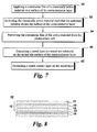
- the method for forming a back contact for a photovoltaic cell includes, at step 30, applying a continuous film 16 of a chemically active material on a surface 15 of the semiconductor layer 14.
- the continuous film 16 has a thickness, which is greater than or equal to 0.5 ⁇ m.
- the thickness of the continuous film is in a range of about 1-10 ⁇ m, and more particularly of about 2-5 ⁇ m.
- the continuous film 16 may be deposited using a variety of techniques, non-limiting examples of which include printing, screen-printing, dipping and spray coating.
- the method further includes, at step 32, activating the chemically active material, such that the activated material etches the surface 15 of the semiconductor layer 14.
- the chemically active material comprises a chemically active paste.
- the term "paste" should be understood to mean a plurality of particles suspended in a binder.
- Non-limiting examples of the chemically active paste include pastes containing high surface area solid particles, such as carbon, silica or alumina, dispersed therein and also optionally containing halogen atoms, such as in the form of hydrochloric acid, chloride salt or iodide salt or organic compounds typically used for ion exchange resins. Although chlorine and iodine are listed as non-limiting examples, the chemically active paste may contain other halogens.
- the chemically active paste comprises a plurality of particles selected from the group consisting of alumina, carbon, boron nitride, silica and combinations thereof and a binder, where the particles are suspended in the binder.
- the binder include water and organic solvents, such as dimethyl esters of dicarboxylic acids. It will be recognized that a variety of binders may be used, and the invention is not limited to a specific binder.
- the chemically active material comprises a graphite paste.
- the graphite paste may be undoped or may be doped with elements from groups IB or IIB of the periodic table of elements and/or elements from group VIA, such as, but not limited to copper (Cu), mercury (Hg), gold (Au), silver (Ag), zinc (Zn), tellurium (Te), selenium (Se), and compounds and combinations thereof, such as Cu/Au- or Cu/HgTe, Ag 2 Te, Ag 3 PO 4 , and Ag 2 MoO 4 , as well as antimony- (Sb), nickel- (Ni), bismuth- (Bi), and lead- (Pb) based compounds.
- groups IB or IIB of the periodic table of elements and/or elements from group VIA such as, but not limited to copper (Cu), mercury (Hg), gold (Au), silver (Ag), zinc (Zn), tellurium (Te), selenium (Se), and compounds and combinations thereof, such as Cu/Au- or
- copper may be introduced into the graphite paste in the form of a class IB-VIA or IIB-VIA or IB-IIB-VIA semiconductor compound, such as copper telluride, mercury telluride, or as a copper dopant in mercury telluride.
- a class IB-VIA or IIB-VIA or IB-IIB-VIA semiconductor compound such as copper telluride, mercury telluride, or as a copper dopant in mercury telluride.
- the introduction of copper in the form of a class IB-VIA or IB-IIB-VIA semiconductor compound instead of using elemental or free copper, may help to prevent the diffusion of copper into the semiconductor layer 14.
- the activation step 32 for the continuous film 16 comprises annealing the photovoltaic cell.
- the photovoltaic cell 10 may be annealed at a temperature in a range of about 100-300 degrees Celsius, for a period in a range of about 5-30 minutes.
- the specific anneal temperatures and times will vary based on the thickness of the film 16 and on the composition of the chemically activated material.
- thermal activation is the example means for activating a graphite paste, other materials may be activated by other means, such as light, and embodiments of the present invention are not restricted to a specific activation means.
- performing the step 32 of activating the chemically active material makes the surface 15 of the CdTe layer 14 tellurium (Te)-rich.
- the surface 15 of the CdTe layer 14 has a Te/ Cd ratio greater than about two (2).
- the relative concentration of Te to Cd at the surface 15 of the CdTe layer 14 can be measured, for example using X-ray Photoelectron Spectroscopy (XPS) and to some extent using Time-Of-Flight Secondary Ion Mass Spectroscopy (TOF-SIMS).
- XPS X-ray Photoelectron Spectroscopy
- TOF-SIMS Time-Of-Flight Secondary Ion Mass Spectroscopy
- the method further includes, at step 34, removing the continuous film 16 of the activated material from the photovoltaic cell 10.
- performing the step 34 of removing the continuous film 16 of the activated material from the photovoltaic cell 10 comprises applying a solvent to the activated material and removing the activated material and the solvent from the photovoltaic cell 10.
- the continuous film 16 comprises a graphite paste
- the solvent comprises dimethylformamide (DMF).
- Other example solvents include water, tetrahydrofuran (THF), and methylethylketone (MEK).
- embodiments of the invention are not limited to the use of specific solvents, but rather the specific solvent selected will vary based upon the specific chemically active material being removed and based upon other requirements, such as environmental and cost considerations.
- the activated material and solvent are removed using non-contact means, such as an air or liquid jet.
- contact means could also be used, for example the partially dissolved material could be scraped or wiped off.
- the step of applying a solution is omitted, and the continuous film 16 is removed by physical means, for example using a laser. It should be recognized that these examples are merely illustrative, and the invention is not limited to a specific technique for removing the continuous film.
- the method for forming a back contact for a photovoltaic cell further includes, at step 36, depositing a metal contact layer 18 on the etched surface 15 of the semiconductor layer.
- the metal contact layer 18 comprises a metal selected from the group consisting of molybdenum, tantalum, tungsten, alloys of molybdenum, tantalum, titanium or tungsten, compounds comprising molybdenum or tungsten (e.g. molybdenumnitride), and combinations thereof.
- the metal contact layer has a thickness of less than or equal to 100 nm.
- the metal contact layer 18 may be deposited using a variety of techniques, non-limiting examples of which include evaporation and sputtering. Moreover, one or more additional metal layers may be disposed on the metal contact layer 18 to form the back contact electrode 12. For example and as indicated in FIG. 3 , an aluminum layer 19 with a thickness in a range of 50-1000 nm may be deposited on a molybdenum contact layer 18. For specific arrangements and as indicated in FIG. 3 , a nickel layer 21 with a thickness in a range of 20-200 nm may be disposed on the aluminum layer 19. For this arrangement, the back contact electrode 12 comprises the molybdenum 18/aluminum 19/nickel 21 stack. In another example, the nickel- is replaced with chromium 21 with an example thickness range of 20-100 nm, such that the back contact electrode 12 comprises the molybdenum 18/aluminum 19/chromium stack 21.
- the method of forming a back contact may optionally include, at step 38, depositing a metal layer 22 on the surface 15 of the semiconductor layer 14 prior to applying the continuous film 16.
- a continuous film of a chemically active material is deposited on the metal layer 22.
- suitable materials for the metal layer 22 include copper, gold, silver, zinc and mercury.
- Example thickness for the metal layer 22 is in a range of about 0.1-10 nm.
- the metal layer 22 may be applied using a variety of techniques, non-limiting examples of which include evaporation and sputtering.
- a very thin Cu-layer 22 is deposited at step 38 on the surface 15 by evaporation, and this process is typically referred to as a Cu-treatment step. Beneficially, 'intermixing' will then occur during the Te-enrichment step.
- Process steps 32, 34 and 36 are then performed, as indicated in FIG. 6 .
- some portion of the metal layer 22 may remain at the surface 15 of the semiconductor layer 14.
- the process parameters may be selected such that all of the metal reacts with the CdTe layer 14, such that none of the metal layer 22 remains at this interface.
- FIGS. 4 and 6 also illustrate an example method for forming a back contact that optionally includes, at step 38, depositing a metal salt solution (also indicated by reference numeral 22 in FIG. 4 ) on the surface 15 of the semiconductor layer 14 prior to applying the continuous film 16.
- a metal salt solution also indicated by reference numeral 22 in FIG. 4
- a Cu-salt solution 22 is sprayed on the surface 15 of the semiconductor layer (14).
- 22 is depicted as a layer in FIG. 4 , one skilled in the art will recognize that the metal-salt spray technique will not result in a continuous metal film.
- a continuous film of a chemically active material is deposited after the Cu-salt solution 22 has been sprayed on the surface 15 of the semiconductor layer.
- Process steps 32, 34 and 36 are then performed, as indicated in FIG. 6 .
- FIGS. 4 , 7 and 8 illustrate an example method for forming a back contact that optionally includes, at step 40, depositing a metal layer 22 on the surface 15 of the semiconductor layer 14 after the continuous film 16 has been removed (at step 34) and prior to applying the metal contact layer 18 (at step 42).
- the back contact electrode 12 also includes optional metal layer 22.
- the metal in layer 22 is selected from IB or IIB groups, such as Cu, Au, Ag, Hg, Zn or a combination thereof.
- metal such as copper, gold, silver, zinc and mercury
- metal may be introduced by adding the respective metal particles, in either elemental or compound form, to the chemically active material prior to its application to the surface 15 of the semiconductor layer 14.
- the above-described method provides back contact electrodes for CdTe PV cells, which exhibit less degradation over the lifetime of the PV cell, as demonstrated by the following example.
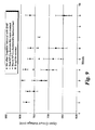
- FIG. 9 illustrates the performance of three types of back contact electrodes for CdTe PV cells that were subjected to temperature accelerated lifetime measurements.
- FIG. 9 shows temperature accelerated open circuit voltage (V oc ) measurements obtained for CdTe cells with three different types of back contact electrodes.
- V oc temperature accelerated open circuit voltage
- the CdTe PV cells were placed in an accelerated lifetime ("ALT") tester, which exposed the devices to a continuous illumination level of 0.7 sun, at a temperature of 65 C, under open circuit conditions. Periodically, the devices were taken out of the ALT-tester, and their performance was measured under standard AM-1.5 conditions.
- FIG. 9 shows the resulting data, plotted as a function of the time that the devices were exposed in the ALT-tester.
- the molybdenum/aluminum back contact electrodes had a 100 nm thick Mo layer (layer 18), followed by 100-1000 nm of Al (layer 19).
- the back-contact of the CdTe was treated with CdCl 2 and then Te-enriched by exposure to a nitric-phosphoric (NP) etch for two minutes.
- NP nitric-phosphoric
- a copper-salt was sprayed onto the etched surface, and the resulting structure was baked.
- Mo/Al back-contact metal layers were deposited.
- the CdTe was sprayed and baked with a Cu-salt and then covered with a graphite paste. A heat treatment was performed before the graphite was covered with the Mo/Al back-contact layers 18, 19.
- a third set of molybdenum/aluminum back contacts were formed using the method of the present invention.
- a Cu-salt was sprayed onto a surface 15 of the CdTe layer 14, which was then baked.
- a continuous film 16 of a graphite paste was formed on the surface 15 of the CdTe layer 14.
- the graphite paste was then activated and removed from the photovoltaic cell 10 using DMF.
- the Mo/Al contact layer 18, 19 was then deposited on the surface 15 of the semiconductor layer exposed by the graphite removal process.
- the molybdenum contacts were 100 nm thick followed by 100 nm of Al.
- the three sets of PV cells were subjected to a continuous illumination level of 0.7 sun, at a temperature of 65 C, under open circuit conditions for a period of 9 weeks, and open circuit voltage measurements were performed weekly.
- the Mo/Al back contacts formed using the method of the present invention exhibited significantly lower degradation during the accelerated lifetime testing than either the graphite contact electrodes or the Molybdenum back contact electrodes formed after the NP-type etch ("NP" in FIG. 9 ).
- V oc degradation appears to be a function of Te-richness and Cu-content.
- the significant degradation of V oc shown in FIG. 9 may be due to continuous interaction between etchants/impurities in the graphite and the rest of the solar cell (primarily interaction between the etchants/impurities in the graphite with the CdTe).
- the present invention significantly reduces these interactions, thereby slowing the V oc degradation of the resulting CdTe cells.
- a particular method for forming an improved back contact 12 for a photovoltaic cell 10 that includes at least one Cadmium Telluride (CdTe) layer 14 is described with reference to FIGS. 1-8 .
- the method includes, at step 30, applying a continuous film 16 of a chemically active material on a surface 15 of the CdTe layer 14.
- the method further includes, at step 32, activating the chemically active material, such that the Tellurium (Te) is enriched on the surface 15 of the CdTe layer 14.
- the method further includes, at step 34, removing the continuous film 16 of the activated material from the photovoltaic cell 10 and, at step 36, depositing a metal contact layer 18 on the Te enriched surface 15 of the CdTe layer 14.
- the surface of the CdTe layer 14 has a Te/Cadmium (Cd) ratio greater than about two (2). According to a more particular embodiment, Te/Cd>3 at the surface 15 of the CdTe layer 14, and still more particularly, Te/Cd > 5 at the surface 15 of the CdTe layer 14.
- the chemically active material comprises a plurality of particles selected from the group consisting of alumina, carbon, boron nitride, silica and combinations thereof and a binder, where the particles are suspended in the binder to form a chemically active paste.
- the step 32 of activating the continuous film 16 comprises annealing the photovoltaic cell
- the metal contact layer 18 comprises a metal selected from the group consisting of molybdenum, tantalum, tungsten, alloys of molybdenum, tantalum and tungsten, compounds comprising molybdenum or tungsten (e.g. molybdenum nitride), and combinations thereof.
- the step 34 of removing the continuous film 16 of the activated material from the photovoltaic cell 10 comprises applying a solvent to the activated material and removing the activated material and the solvent from the photovoltaic cell 10.
- the method optionally includes, at step 38, depositing a metal layer 22 on the surface 15 of the CdTe layer 14 prior to applying the continuous film 16.
- the method optionally includes, at step 40, depositing a metal layer (or a metal salt solution) 22 on the surface 15 of the CdTe layer 14 after the continuous film 16 has been removed and prior to applying the metal contact layer 18.
- a metal layer or a metal salt solution 22
- FIG. 8 An example resulting back contact is shown in FIG. 8 .
- the photovoltaic cell 10 with a back contact 12 made using the above-described methods may have the following desirable properties.
- a surface 15 of the CdTe layer 14 has a tellurium (Te)/cadmium (Cd) ratio greater than about two (2).
- Te/Cd >3 at the surface 15 of the CdTe layer 14, and still more particularly, Te/Cd > 5 at the surface 15 of the CdTe layer 14.
- the CdTe layer 14 is Te enriched only at the surface 15 and not along the grain-boundaries.
- the resulting PV cells have back contact electrodes, which exhibit less degradation over the lifetime of the PV cell.
- back contact electrodes By improving the stability of the back contact for the PV cells, higher outputs are achieved over the lifetime for the PV cells, as well as higher end of life-efficiency for the PV devices.
Landscapes
- Photovoltaic Devices (AREA)
- Electrodes Of Semiconductors (AREA)
- Life Sciences & Earth Sciences (AREA)
- Engineering & Computer Science (AREA)
- Sustainable Development (AREA)
- Sustainable Energy (AREA)
Abstract


Description
- The invention relates generally to photovoltaic cells and, more particularly, to methods for forming back contact electrodes for photovoltaic cells.
- Solar energy is abundant in many parts of the world year round. Thus, photovoltaic (PV) devices, which convert solar energy into electrical energy, have the potential to provide a reliable form of clean, renewable energy in many parts of the world. Typically, in its basic form, a PV (or solar) cell includes a semiconductor junction made of two or three layers that are disposed on a substrate layer, and two contacts (electrically conductive layers) for passing electrical energy in the form of electrical current to an external circuit. Moreover, additional layers are often employed to enhance the conversion efficiency of the PV device.
- There are a variety of candidate material systems for PV cells, each of which has certain advantages and disadvantages. Cadmium telluride (CdTe) is a prominent polycrystalline thin-film material, with a nearly ideal bandgap of about 1.45-1.5 electron volts. CdTe also has a very high absorptivity, and films of CdTe can be manufactured using low-cost techniques. In theory, solar cell efficiencies in excess of twenty percent (20%) could be achieved for cadmium sulfide (CdS)/CdTe devices, provided various issues with the quality of the individual semiconductor layers and with the back contact electrode can be overcome.
- Because of the high work function of CdTe, conventional metal back contacts are not generally viewed as being suitable. Instead, graphite pastes (either undoped or doped, for example with copper or mercury) are widely used as a back contact for CdTe PV cells. However, these graphite-paste back contacts tend to degrade significantly over time, as can be shown via accelerated lifetime testing. This degradation typically manifests itself as a decrease in fill factor (FF) and/or open circuit voltage V OC over time. The fill factor degradation is typically driven by a decrease in shunt resistance (R sh) and an increase in the series resistance (R OC) over time. The degradation of the back contact electrodes undesirably leads to degradation of the solar cell efficiency, on a long-term basis.
- To date, the failure to develop low-resistance contacts has hindered the commercialization of CdTe solar cells. A cost-effective solution to this problem would remove one of the remaining hurdles for commercializing CdTe photovoltaic modules.
- It would therefore be desirable to provide a back contact electrode for a CdTe PV cell, which exhibits less degradation over the lifetime of the PV cell. It would further be desirable to provide an economical method for forming the improved back contact electrode, in order to facilitate commercialization of CdTe PV cells.
- One aspect of the present invention resides in a method for forming a back contact for a photovoltaic cell that includes at least one semiconductor layer. The method includes applying a continuous film of a chemically active material on a surface of the semiconductor layer and activating the chemically active material, such that the activated material etches the surface of the semiconductor layer. The method further includes removing the continuous film of the activated material from the photovoltaic cell and depositing a metal contact layer on the etched surface of the semiconductor layer.
- Another aspect of the present invention resides in a method for forming a back contact for a photovoltaic cell that includes at least one cadmium telluride (CdTe) layer. The method includes applying a continuous film of a chemically active material on a surface of the CdTe layer and activating the chemically active material such that the surface of the CdTe layer is enriched with tellurium (Te). The method further includes removing the continuous film of the activated material from the photovoltaic cell and depositing a metal contact layer on the Te enriched surface of the CdTe layer.
- Various features, aspects, and advantages of the present invention will become better understood when the following detailed description is read with reference to the accompanying drawings in which like characters represent like parts throughout the drawings, wherein:
-
FIG. 1 illustrates a first processing step for forming a back contact electrode; -
FIG. 2 illustrates a subsequent processing step for forming a back contact electrode; -
FIG. 3 illustrates an example back contact electrode structure; -
FIG. 4 illustrates a metal treatment step, where the metal may be deposited as a metal or as a metal-salt; -
FIG. 5 illustrates an example method for forming a back contact for a photovoltaic cell; -
FIG. 6 illustrates an additional optional processing step for the method shown inFIG. 5 ; -
FIG. 7 illustrates an additional optional processing step for the method shown inFIG. 5 ; -
FIG. 8 illustrates another example back contact electrode structure; and -
FIG. 9 is a graph showing the results of temperature accelerated lifetime measurements for different types of back contact electrodes. - As noted above, the high work function of CdTe leaves a relatively small set of metals that can be employed to form an ohmic contact with the CdTe layer. Suitable metals include platinum and gold, which are not commercially viable candidates for low-cost CdTe PV cells. However, lower cost metals, such as molybdenum, nickel, and chromium, typically form a tunneling barrier at the interface between the back contact and the CdTe layer. As CdTe typically has carrier densities between about 1 x 10¹⁴ to about 1 x 10¹⁵ per cubic centimeter, this tunneling barrier may be relatively large. Thus, absent proper treatment of the backside of the CdTe layer, the resistance with the back contact layer can be significant, thereby reducing the fill factor (and hence the efficiency) of the PV cell.
- Various aspects of the present invention address these issues, and a method for forming an improved
back contact 12 for aphotovoltaic cell 10 may be provided. The method is described with reference toFIGS. 1-8 . As indicated, for example, inFIG. 3 , thephotovoltaic cell 10 includes at least onesemiconductor layer 14. For the illustrated arrangements, thesemiconductor layer 14 comprises cadmium telluride (CdTe). Although the examples provided are directed to CdTe, the invention can be used to form improved back contact electrodes for other semiconductors as well. Other example materials forsemiconductor layer 14 include, without limitation, CdZnTe and ZnTe. - As indicated, for example, in
FIGS. 1 and5 , the method for forming a back contact for a photovoltaic cell includes, atstep 30, applying acontinuous film 16 of a chemically active material on asurface 15 of thesemiconductor layer 14. For certain example arrangements, thecontinuous film 16 has a thickness, which is greater than or equal to 0.5 µm. For more particular examples, the thickness of the continuous film is in a range of about 1-10 µm, and more particularly of about 2-5 µm. Thecontinuous film 16 may be deposited using a variety of techniques, non-limiting examples of which include printing, screen-printing, dipping and spray coating. - As indicated in
FIG. 5 , the method further includes, atstep 32, activating the chemically active material, such that the activated material etches thesurface 15 of thesemiconductor layer 14. For particular examples, the chemically active material comprises a chemically active paste. As used here, the term "paste" should be understood to mean a plurality of particles suspended in a binder. Non-limiting examples of the chemically active paste include pastes containing high surface area solid particles, such as carbon, silica or alumina, dispersed therein and also optionally containing halogen atoms, such as in the form of hydrochloric acid, chloride salt or iodide salt or organic compounds typically used for ion exchange resins. Although chlorine and iodine are listed as non-limiting examples, the chemically active paste may contain other halogens. - For more particular examples, the chemically active paste comprises a plurality of particles selected from the group consisting of alumina, carbon, boron nitride, silica and combinations thereof and a binder, where the particles are suspended in the binder. Non-limiting examples of the binder include water and organic solvents, such as dimethyl esters of dicarboxylic acids. It will be recognized that a variety of binders may be used, and the invention is not limited to a specific binder.
- For certain examples the chemically active material comprises a graphite paste. The graphite paste may be undoped or may be doped with elements from groups IB or IIB of the periodic table of elements and/or elements from group VIA, such as, but not limited to copper (Cu), mercury (Hg), gold (Au), silver (Ag), zinc (Zn), tellurium (Te), selenium (Se), and compounds and combinations thereof, such as Cu/Au- or Cu/HgTe, Ag2Te, Ag3PO4, and Ag2MoO4, as well as antimony- (Sb), nickel- (Ni), bismuth- (Bi), and lead- (Pb) based compounds. For certain examples, copper may be introduced into the graphite paste in the form of a class IB-VIA or IIB-VIA or IB-IIB-VIA semiconductor compound, such as copper telluride, mercury telluride, or as a copper dopant in mercury telluride. Beneficially, the introduction of copper in the form of a class IB-VIA or IB-IIB-VIA semiconductor compound, instead of using elemental or free copper, may help to prevent the diffusion of copper into the
semiconductor layer 14. - For particular embodiments, the
activation step 32 for thecontinuous film 16 comprises annealing the photovoltaic cell. In one non-limiting example, thephotovoltaic cell 10 may be annealed at a temperature in a range of about 100-300 degrees Celsius, for a period in a range of about 5-30 minutes. However, it will be recognized that the specific anneal temperatures and times will vary based on the thickness of thefilm 16 and on the composition of the chemically activated material. In addition, although thermal activation is the example means for activating a graphite paste, other materials may be activated by other means, such as light, and embodiments of the present invention are not restricted to a specific activation means. - According to more particular embodiments, performing the
step 32 of activating the chemically active material makes thesurface 15 of theCdTe layer 14 tellurium (Te)-rich. For particular examples, thesurface 15 of theCdTe layer 14 has a Te/ Cd ratio greater than about two (2). According to a more particular embodiment, the ratio Te/Cd > 3 at the surface (15) of theCdTe layer 14, and still more particularly, Te/Cd > 5 at thesurface 15 of theCdTe layer 14. The Te enrichment is the highest at thesurface 15 and tapers off as one moves deeper inside theCdTe layer 14, such that Te/Cd=1 at a certain depth within theCdTe layer 14. The relative concentration of Te to Cd at thesurface 15 of theCdTe layer 14 can be measured, for example using X-ray Photoelectron Spectroscopy (XPS) and to some extent using Time-Of-Flight Secondary Ion Mass Spectroscopy (TOF-SIMS). - Returning to
FIG. 5 , the method further includes, atstep 34, removing thecontinuous film 16 of the activated material from thephotovoltaic cell 10. For particular examples, performing thestep 34 of removing thecontinuous film 16 of the activated material from thephotovoltaic cell 10 comprises applying a solvent to the activated material and removing the activated material and the solvent from thephotovoltaic cell 10. In one non-limiting example, thecontinuous film 16 comprises a graphite paste, and the solvent comprises dimethylformamide (DMF). Other example solvents include water, tetrahydrofuran (THF), and methylethylketone (MEK). However, embodiments of the invention are not limited to the use of specific solvents, but rather the specific solvent selected will vary based upon the specific chemically active material being removed and based upon other requirements, such as environmental and cost considerations. For certain implementations, the activated material and solvent are removed using non-contact means, such as an air or liquid jet. However, in other implementations, contact means could also be used, for example the partially dissolved material could be scraped or wiped off. For other example configurations, the step of applying a solution is omitted, and thecontinuous film 16 is removed by physical means, for example using a laser. It should be recognized that these examples are merely illustrative, and the invention is not limited to a specific technique for removing the continuous film. - As indicated, for example, in
FIGS. 2 and5 , the method for forming a back contact for a photovoltaic cell further includes, atstep 36, depositing ametal contact layer 18 on the etchedsurface 15 of the semiconductor layer. For particular configurations, themetal contact layer 18 comprises a metal selected from the group consisting of molybdenum, tantalum, tungsten, alloys of molybdenum, tantalum, titanium or tungsten, compounds comprising molybdenum or tungsten (e.g. molybdenumnitride), and combinations thereof. In one non-limiting example, the metal contact layer has a thickness of less than or equal to 100 nm. Themetal contact layer 18 may be deposited using a variety of techniques, non-limiting examples of which include evaporation and sputtering. Moreover, one or more additional metal layers may be disposed on themetal contact layer 18 to form theback contact electrode 12. For example and as indicated inFIG. 3 , analuminum layer 19 with a thickness in a range of 50-1000 nm may be deposited on amolybdenum contact layer 18. For specific arrangements and as indicated inFIG. 3 , anickel layer 21 with a thickness in a range of 20-200 nm may be disposed on thealuminum layer 19. For this arrangement, theback contact electrode 12 comprises themolybdenum 18/aluminum 19/nickel 21 stack. In another example, the nickel- is replaced withchromium 21 with an example thickness range of 20-100 nm, such that theback contact electrode 12 comprises themolybdenum 18/aluminum 19/chromium stack 21. - In addition and as indicated in
FIGS. 4 and6 , for example, the method of forming a back contact may optionally include, atstep 38, depositing ametal layer 22 on thesurface 15 of thesemiconductor layer 14 prior to applying thecontinuous film 16. For this embodiment, at step 30 a continuous film of a chemically active material is deposited on themetal layer 22. Non-limiting examples of suitable materials for themetal layer 22 include copper, gold, silver, zinc and mercury. Example thickness for themetal layer 22 is in a range of about 0.1-10 nm. Themetal layer 22 may be applied using a variety of techniques, non-limiting examples of which include evaporation and sputtering. In one non-limiting example, a very thin Cu-layer 22 is deposited atstep 38 on thesurface 15 by evaporation, and this process is typically referred to as a Cu-treatment step. Beneficially, 'intermixing' will then occur during the Te-enrichment step. Process steps 32, 34 and 36 are then performed, as indicated inFIG. 6 . Although not shown in the illustrations, under certain processing conditions, some portion of themetal layer 22 may remain at thesurface 15 of thesemiconductor layer 14. However, the process parameters may be selected such that all of the metal reacts with theCdTe layer 14, such that none of themetal layer 22 remains at this interface. -
FIGS. 4 and6 also illustrate an example method for forming a back contact that optionally includes, atstep 38, depositing a metal salt solution (also indicated byreference numeral 22 inFIG. 4 ) on thesurface 15 of thesemiconductor layer 14 prior to applying thecontinuous film 16. In one non-limiting example, a Cu-salt solution 22 is sprayed on thesurface 15 of the semiconductor layer (14). Although 22 is depicted as a layer inFIG. 4 , one skilled in the art will recognize that the metal-salt spray technique will not result in a continuous metal film. For this process, atstep 30, a continuous film of a chemically active material is deposited after the Cu-salt solution 22 has been sprayed on thesurface 15 of the semiconductor layer. Process steps 32, 34 and 36 are then performed, as indicated inFIG. 6 . -
FIGS. 4 ,7 and 8 illustrate an example method for forming a back contact that optionally includes, atstep 40, depositing ametal layer 22 on thesurface 15 of thesemiconductor layer 14 after thecontinuous film 16 has been removed (at step 34) and prior to applying the metal contact layer 18 (at step 42). For the resulting arrangement shown inFIG. 8 , theback contact electrode 12 also includesoptional metal layer 22. For particular configurations, the metal inlayer 22 is selected from IB or IIB groups, such as Cu, Au, Ag, Hg, Zn or a combination thereof. - In addition to the optional process steps discussed above with reference to
FIGS. 6 and7 , metal, such as copper, gold, silver, zinc and mercury, may be introduced by adding the respective metal particles, in either elemental or compound form, to the chemically active material prior to its application to thesurface 15 of thesemiconductor layer 14. - Beneficially, the above-described method provides back contact electrodes for CdTe PV cells, which exhibit less degradation over the lifetime of the PV cell, as demonstrated by the following example.
-
FIG. 9 illustrates the performance of three types of back contact electrodes for CdTe PV cells that were subjected to temperature accelerated lifetime measurements. In particular,FIG. 9 shows temperature accelerated open circuit voltage (Voc) measurements obtained for CdTe cells with three different types of back contact electrodes. After fabrication, the CdTe PV cells were placed in an accelerated lifetime ("ALT") tester, which exposed the devices to a continuous illumination level of 0.7 sun, at a temperature of 65 C, under open circuit conditions. Periodically, the devices were taken out of the ALT-tester, and their performance was measured under standard AM-1.5 conditions.FIG. 9 shows the resulting data, plotted as a function of the time that the devices were exposed in the ALT-tester. - Three processes were employed to fabricate back contact electrodes for CdTe PV cells. For all three processes, the molybdenum/aluminum back contact electrodes had a 100 nm thick Mo layer (layer 18), followed by 100-1000 nm of Al (layer 19).
- In the first process, the back-contact of the CdTe was treated with CdCl2 and then Te-enriched by exposure to a nitric-phosphoric (NP) etch for two minutes. Next, a copper-salt was sprayed onto the etched surface, and the resulting structure was baked. Next, Mo/Al back-contact metal layers were deposited.
- In the second process, the CdTe was sprayed and baked with a Cu-salt and then covered with a graphite paste. A heat treatment was performed before the graphite was covered with the Mo/Al back-
contact layers - A third set of molybdenum/aluminum back contacts were formed using the method of the present invention. First, a Cu-salt was sprayed onto a
surface 15 of theCdTe layer 14, which was then baked. Next, acontinuous film 16 of a graphite paste was formed on thesurface 15 of theCdTe layer 14. The graphite paste was then activated and removed from thephotovoltaic cell 10 using DMF. The Mo/Al contact layer surface 15 of the semiconductor layer exposed by the graphite removal process. The molybdenum contacts were 100 nm thick followed by 100 nm of Al. - The three sets of PV cells were subjected to a continuous illumination level of 0.7 sun, at a temperature of 65 C, under open circuit conditions for a period of 9 weeks, and open circuit voltage measurements were performed weekly. As shown in
FIG. 9 , the Mo/Al back contacts formed using the method of the present invention exhibited significantly lower degradation during the accelerated lifetime testing than either the graphite contact electrodes or the Molybdenum back contact electrodes formed after the NP-type etch ("NP" inFIG. 9 ). - In addition, there was a wide range of performance for the NP electrodes, with the best NP back contact electrodes exhibiting performance superior to that of the graphite contact electrodes, and with the worst NP back contact electrodes degrading more rapidly than the graphite back contact electrodes, as shown in
FIG. 9 . - Although the cause of Voc degradation of CdTe solar cells is complex, one possible theory is that Voc degradation appears to be a function of Te-richness and Cu-content. For the 'loaded' graphite contacts, the significant degradation of Voc shown in
FIG. 9 may be due to continuous interaction between etchants/impurities in the graphite and the rest of the solar cell (primarily interaction between the etchants/impurities in the graphite with the CdTe). By removing the chemicallyactive film 16 prior to depositing the metal back contact, the present invention significantly reduces these interactions, thereby slowing the Voc degradation of the resulting CdTe cells. For the "NP" contacts, grain-boundary attack of the NP etchant appears to cause shunting paths in the device, negatively impacting the Voc. The present invention avoids this grain-boundary etching, because the paste does not penetrate into the grain-boundaries, as solutions, like NP, do. In addition, continuous exposure to the paste (as occurs for the graphite contacts) will eventually start etching the grain-boundaries, likely due to vapors forming in the spaces between the paste and the grain-boundaries. - A particular method for forming an
improved back contact 12 for aphotovoltaic cell 10 that includes at least one Cadmium Telluride (CdTe)layer 14 is described with reference toFIGS. 1-8 . As shown for example inFIGS. 1 and5 , the method includes, atstep 30, applying acontinuous film 16 of a chemically active material on asurface 15 of theCdTe layer 14. The method further includes, atstep 32, activating the chemically active material, such that the Tellurium (Te) is enriched on thesurface 15 of theCdTe layer 14. The method further includes, atstep 34, removing thecontinuous film 16 of the activated material from thephotovoltaic cell 10 and, atstep 36, depositing ametal contact layer 18 on the Te enrichedsurface 15 of theCdTe layer 14. - According to a particular embodiment, the surface of the
CdTe layer 14 has a Te/Cadmium (Cd) ratio greater than about two (2). According to a more particular embodiment, Te/Cd>3 at thesurface 15 of theCdTe layer 14, and still more particularly, Te/Cd > 5 at thesurface 15 of theCdTe layer 14. - According to a particular embodiment, the chemically active material comprises a plurality of particles selected from the group consisting of alumina, carbon, boron nitride, silica and combinations thereof and a binder, where the particles are suspended in the binder to form a chemically active paste.
- According to a particular embodiment, the
step 32 of activating thecontinuous film 16 comprises annealing the photovoltaic cell, and themetal contact layer 18 comprises a metal selected from the group consisting of molybdenum, tantalum, tungsten, alloys of molybdenum, tantalum and tungsten, compounds comprising molybdenum or tungsten (e.g. molybdenum nitride), and combinations thereof. For this particular embodiment, thestep 34 of removing thecontinuous film 16 of the activated material from thephotovoltaic cell 10 comprises applying a solvent to the activated material and removing the activated material and the solvent from thephotovoltaic cell 10. - As shown for example in
FIGS. 4 and6 , the method optionally includes, atstep 38, depositing ametal layer 22 on thesurface 15 of theCdTe layer 14 prior to applying thecontinuous film 16. - As shown for example in
FIG. 7 , the method optionally includes, atstep 40, depositing a metal layer (or a metal salt solution) 22 on thesurface 15 of theCdTe layer 14 after thecontinuous film 16 has been removed and prior to applying themetal contact layer 18. An example resulting back contact is shown inFIG. 8 . - For particular embodiments, the
photovoltaic cell 10 with aback contact 12 made using the above-described methods may have the following desirable properties. For certain configurations, asurface 15 of theCdTe layer 14 has a tellurium (Te)/cadmium (Cd) ratio greater than about two (2). According to a more particular embodiment, Te/Cd >3 at thesurface 15 of theCdTe layer 14, and still more particularly, Te/Cd > 5 at thesurface 15 of theCdTe layer 14. For particular embodiments, theCdTe layer 14 is Te enriched only at thesurface 15 and not along the grain-boundaries. - Beneficially, the resulting PV cells have back contact electrodes, which exhibit less degradation over the lifetime of the PV cell. By improving the stability of the back contact for the PV cells, higher outputs are achieved over the lifetime for the PV cells, as well as higher end of life-efficiency for the PV devices.
- Although only certain features of the invention have been illustrated and described herein, many modifications and changes will occur to those skilled in the art. It is, therefore, to be understood that the appended claims are intended to cover all such modifications and changes as fall within the true spirit of the invention.
- Various aspects and embodiments of the present invention are defined by the following numbered clauses:
- 1. A method for forming a back contact for a photovoltaic cell that includes at least one semiconductor layer, the method comprising:
- applying a continuous film of a chemically active material on a surface of the semiconductor layer;
- activating the chemically active material such that the activated material etches the surface of the semiconductor layer;
- removing the continuous film of the activated material from the photovoltaic cell; and
- depositing a metal contact layer on the etched surface of the semiconductor layer.
- 2. The method of
clause 1, wherein the chemically active material comprises a chemically active paste. - 3. The method of any preceding clause, wherein the chemically active paste comprises:
- a plurality of particles selected from the group consisting of alumina, carbon, boron nitride, silica and combinations thereof; and
- a binder, wherein the particles are suspended in the binder.
- 4. The method of any preceding clause, wherein the chemically active material comprises a carbon paste.
- 5. The method of any preceding clause, wherein activating the continuous film comprises annealing the photovoltaic cell.
- 6. The method of any preceding clause, wherein the continuous film has a thickness, which is greater than or equal to 0.5 µm.
- 7. The method of any preceding clause, wherein the metal contact layer comprises a metal selected from the group consisting of molybdenum, tantalum, tungsten, alloys of molybdenum, tantalum or tungsten, compounds comprising molybdenum or tungsten, and combinations thereof.
- 8. The method of any preceding clause, wherein the semiconductor layer comprises cadmium telluride (CdTe).
- 9. The method of any preceding clause, wherein performing the step of activating the chemically active material makes the surface of the CdTe layer tellurium (Te)-rich.
- 10. The method of any preceding clause, wherein the surface of the CdTe layer has a tellurium (Te)/cadmium (Cd) ratio greater than about two (2).
- 11. The method of any preceding clause, wherein performing the step of removing the continuous film of the activated material from the photovoltaic cell comprises:
- applying a solvent to the activated material; and
- removing the activated material and the solvent from the photovoltaic cell.
- 12. The method of any preceding clause, further comprising depositing a metal layer on the surface of the semiconductor layer prior to applying the continuous film.
- 13. The method of any preceding clause, further comprising depositing a metal salt solution on the surface of the semiconductor layer prior to applying the continuous film.
- 14. The method of any preceding clause, further comprising depositing a metal layer on the surface of the semiconductor layer after the continuous film has been removed and prior to applying the metal contact layer.
- 15. The method of any preceding clause, further comprising depositing a metal salt solution on the surface of the semiconductor layer after the continuous film has been removed and prior to applying the metal contact layer.
- 16. A method for forming a back contact for a photovoltaic cell that includes at least one cadmium telluride (CdTe) layer, the method comprising:
- applying a continuous film of a chemically active material on a surface of the CdTe layer;
- activating the chemically active material such that the surface of the CdTe layer is enriched with tellurium (Te);
- removing the continuous film of the activated material from the photovoltaic cell; and
- depositing a metal contact layer on the Te enriched surface of the CdTe layer.
- 17. The method of any preceding clause, wherein the surface of the CdTe layer has a tellurium (Te)/cadmium (Cd) ratio greater than about two (2).
- 18. The method of any preceding clause, wherein the chemically active material comprises:
- a plurality of particles selected from the group consisting of alumina, carbon, boron nitride, silica and combinations thereof; and
- a binder, wherein the particles are suspended in the binder to form a chemically active paste.
- 19. The method of any preceding clause, wherein activating the continuous film comprises annealing the photovoltaic cell, wherein the metal contact layer comprises a metal selected from the group consisting of molybdenum, tantalum, tungsten, alloys of molybdenum, tantalum and tungsten, compounds comprising molybdenum or tungsten, and combinations thereof, and wherein performing the step of removing the continuous film of the activated material from the photovoltaic cell comprises:
- applying a solvent to the activated material; and
- removing the activated material and the solvent from the photovoltaic cell.
- 20. The method of any preceding clause, further comprising depositing a metal layer or a metal salt solution on the surface of the CdTe layer prior to applying the continuous film.
- 21. The method of any preceding clause, further comprising depositing a metal layer or a metal salt solution on the surface of the CdTe layer after the continuous film has been removed and prior to applying the metal contact layer.
- 22. A photovoltaic cell with a back contact made using the method of any preceding clause.
- 23. The photovoltaic cell (10) of any preceding clause, wherein a surface of the CdTe layer has a tellurium (Te)/cadmium (Cd) ratio greater than about two (2).
- 24. The photovoltaic cell of any preceding clause, comprising a CdTe layer with a Te enriched surface and a plurality of grain boundaries, wherein the CdTe layer is not Te enriched along the grain-boundaries.
Claims (10)
- A method for forming a back contact (12) for a photovoltaic cell (10) that includes at least one semiconductor layer (14), the method comprising:applying a continuous film (16) of a chemically active material on a surface (15) of the semiconductor layer (14);activating the chemically active material such that the activated material etches the surface (15) of the semiconductor layer (14);removing the continuous film (16) of the activated material from the photovoltaic cell (10); anddepositing a metal contact layer (18) on the etched surface (15) of the semiconductor layer.
- The method of Claim 1, wherein the chemically active material comprises a chemically active paste comprising:a plurality of particles selected from the group consisting of alumina, carbon, boron nitride, silica and combinations thereof; anda binder, wherein the particles are suspended in the binder.
- The method of any preceding Claim, wherein activating the continuous film (16) comprises annealing the photovoltaic cell,
wherein the continuous film (16) has a thickness, which is greater than or equal to 0.5 µm, and
wherein the metal contact layer (18) comprises a metal selected from the group consisting of molybdenum, tantalum, tungsten, alloys of molybdenum, tantalum or tungsten, compounds comprising molybdenum or tungsten, and combinations thereof. - The method of any preceding Claim, wherein the semiconductor layer (14) comprises cadmium telluride (CdTe), and wherein performing the step of activating the chemically active material makes the surface (15) of the CdTe layer (14) tellurium (Te)-rich.
- The method of any preceding Claim, further comprising depositing a metal layer (22) or a metal salt solution (22) on the surface (15) of the semiconductor layer (14) prior to applying the continuous film (16).
- The method of any preceding Claim, further comprising depositing a metal layer (22) or a metal salt solution (22) on the surface (15) of the semiconductor layer (14) after the continuous film (16) has been removed and prior to applying the metal contact layer (18).
- A method for forming a back contact (12) for a photovoltaic cell (10) that includes at least one cadmium telluride (CdTe) layer (14), the method comprising:applying a continuous film (16) of a chemically active material on a surface (15) of the CdTe layer (14);activating the chemically active material such that the surface (15) of the CdTe layer (14)is enriched with tellurium (Te);removing the continuous film (16) of the activated material from the photovoltaic cell (10); anddepositing a metal contact layer (18) on the Te enriched surface (15) of the CdTe layer.
- The method of Claim 7, wherein activating the continuous film (16) comprises annealing the photovoltaic cell, wherein the metal contact layer (18) comprises a metal selected from the group consisting of molybdenum, tantalum, tungsten, alloys of molybdenum, tantalum and tungsten, compounds comprising molybdenum or tungsten, and combinations thereof, and wherein performing the step of removing the continuous film (16) of the activated material from the photovoltaic cell (10) comprises:applying a solvent to the activated material; andremoving the activated material and the solvent from the photovoltaic cell (10).
- A photovoltaic cell (10) with a back contact (12) made using the method of any preceding Claim.
- The photovoltaic cell (10) of Claim 9, wherein a surface (15) of the CdTe layer (14) has a tellurium (Te)/cadmium (Cd) ratio greater than about two (2).
Applications Claiming Priority (1)
| Application Number | Priority Date | Filing Date | Title |
|---|---|---|---|
| US12/765,225 US8524524B2 (en) | 2010-04-22 | 2010-04-22 | Methods for forming back contact electrodes for cadmium telluride photovoltaic cells |
Publications (3)
| Publication Number | Publication Date |
|---|---|
| EP2381486A2 true EP2381486A2 (en) | 2011-10-26 |
| EP2381486A3 EP2381486A3 (en) | 2015-04-15 |
| EP2381486B1 EP2381486B1 (en) | 2020-06-03 |
Family
ID=44474945
Family Applications (1)
| Application Number | Title | Priority Date | Filing Date |
|---|---|---|---|
| EP11163286.5A Active EP2381486B1 (en) | 2010-04-22 | 2011-04-20 | Method for forming back contact electrodes for cadmium telluride photovoltaic cells |
Country Status (4)
| Country | Link |
|---|---|
| US (2) | US8524524B2 (en) |
| EP (1) | EP2381486B1 (en) |
| CN (1) | CN102237445B (en) |
| AU (1) | AU2011201681B2 (en) |
Cited By (2)
| Publication number | Priority date | Publication date | Assignee | Title |
|---|---|---|---|---|
| EP2973731A1 (en) * | 2013-03-15 | 2016-01-20 | First Solar, Inc | Photovoltaic device having improved back electrode and method of formation |
| EP3025374A4 (en) * | 2013-07-25 | 2017-03-15 | First Solar, Inc | Tellurium enriched back contact paste with copper |
Families Citing this family (20)
| Publication number | Priority date | Publication date | Assignee | Title |
|---|---|---|---|---|
| US9495386B2 (en) | 2008-03-05 | 2016-11-15 | Ebay Inc. | Identification of items depicted in images |
| EP3239919A1 (en) | 2008-03-05 | 2017-11-01 | eBay Inc. | Method and apparatus for image recognition services |
| US8524524B2 (en) | 2010-04-22 | 2013-09-03 | General Electric Company | Methods for forming back contact electrodes for cadmium telluride photovoltaic cells |
| JP5792523B2 (en) * | 2010-06-18 | 2015-10-14 | 株式会社半導体エネルギー研究所 | Method for manufacturing photoelectric conversion device |
| US9147793B2 (en) | 2011-06-20 | 2015-09-29 | Alliance For Sustainable Energy, Llc | CdTe devices and method of manufacturing same |
| US8822261B2 (en) * | 2011-09-26 | 2014-09-02 | First Solar, Inc. | Methods of making photovoltaic devices |
| KR101272997B1 (en) * | 2011-10-18 | 2013-06-10 | 엘지이노텍 주식회사 | Solar cell apparatus and method of fabricating the same |
| US10846766B2 (en) | 2012-06-29 | 2020-11-24 | Ebay Inc. | Contextual menus based on image recognition |
| US20140060634A1 (en) * | 2012-08-31 | 2014-03-06 | Primestar Solar, Inc. | Use of an inert graphite layer in a back contact of a photovoltaic cell |
| US9117956B2 (en) | 2012-08-31 | 2015-08-25 | First Solar, Inc. | Method of controlling the amount of Cu doping when forming a back contact of a photovoltaic cell |
| US9276157B2 (en) * | 2012-08-31 | 2016-03-01 | First Solar, Inc. | Methods of treating a semiconductor layer |
| US9231134B2 (en) * | 2012-08-31 | 2016-01-05 | First Solar, Inc. | Photovoltaic devices |
| US8697480B1 (en) | 2012-11-21 | 2014-04-15 | First Solar, Inc. | Method for treating a semiconductor |
| CN102983219B (en) * | 2012-12-03 | 2015-04-15 | 深圳先进技术研究院 | Preparation method of thin-film solar cell component |
| US9276147B2 (en) | 2012-12-13 | 2016-03-01 | First Solar, Inc. | Methods of fabricating a photovoltaic module, and related system |
| US9306105B2 (en) | 2013-07-31 | 2016-04-05 | First Solar Malaysia Sdn. Bhd. | Finger structures protruding from absorber layer for improved solar cell back contact |
| KR101696968B1 (en) * | 2014-01-09 | 2017-01-16 | 제일모직주식회사 | Composition for forming solar cell electrode and electrode prepared using the same |
| DE102014208029A1 (en) * | 2014-04-29 | 2015-10-29 | China Triumph International Engineering Co., Ltd. | Additional temperature treatment step for thin-film solar cells |
| JP6689456B2 (en) | 2016-10-12 | 2020-04-28 | ファースト・ソーラー・インコーポレーテッド | Photovoltaic device with transparent tunnel junction |
| WO2018119679A1 (en) * | 2016-12-27 | 2018-07-05 | China Triumph International Engineering Co., Ltd. | Method for activation of cdte layer of cdte thin-film solar cells with calcium hypochlorite |
Family Cites Families (62)
| Publication number | Priority date | Publication date | Assignee | Title |
|---|---|---|---|---|
| US4319069A (en) * | 1980-07-25 | 1982-03-09 | Eastman Kodak Company | Semiconductor devices having improved low-resistance contacts to p-type CdTe, and method of preparation |
| US4456630A (en) | 1983-08-18 | 1984-06-26 | Monosolar, Inc. | Method of forming ohmic contacts |
| US4680611A (en) * | 1984-12-28 | 1987-07-14 | Sohio Commercial Development Co. | Multilayer ohmic contact for p-type semiconductor and method of making same |
| US4734381A (en) * | 1985-10-24 | 1988-03-29 | Atlantic Richfield Company | Method of making a thin film cadmium telluride solar cell |
| US5698451A (en) * | 1988-06-10 | 1997-12-16 | Mobil Solar Energy Corporation | Method of fabricating contacts for solar cells |
| US5296043A (en) * | 1990-02-16 | 1994-03-22 | Canon Kabushiki Kaisha | Multi-cells integrated solar cell module and process for producing the same |
| US5501744A (en) * | 1992-01-13 | 1996-03-26 | Photon Energy, Inc. | Photovoltaic cell having a p-type polycrystalline layer with large crystals |
| US5557146A (en) | 1993-07-14 | 1996-09-17 | University Of South Florida | Ohmic contact using binder paste with semiconductor material dispersed therein |
| US5688366A (en) * | 1994-04-28 | 1997-11-18 | Canon Kabushiki Kaisha | Etching method, method of producing a semiconductor device, and etchant therefor |
| JP3057599B2 (en) * | 1994-07-06 | 2000-06-26 | キヤノン株式会社 | Cleaning device and cleaning method |
| EP0729189A1 (en) * | 1995-02-21 | 1996-08-28 | Interuniversitair Micro-Elektronica Centrum Vzw | Method of preparing solar cells and products obtained thereof |
| US5804463A (en) * | 1995-06-05 | 1998-09-08 | Raytheon Ti Systems, Inc. | Noble metal diffusion doping of mercury cadmium telluride for use in infrared detectors |
| US6169246B1 (en) * | 1998-09-08 | 2001-01-02 | Midwest Research Institute | Photovoltaic devices comprising zinc stannate buffer layer and method for making |
| US6137048A (en) * | 1996-11-07 | 2000-10-24 | Midwest Research Institute | Process for fabricating polycrystalline semiconductor thin-film solar cells, and cells produced thereby |
| EP0881694A1 (en) * | 1997-05-30 | 1998-12-02 | Interuniversitair Micro-Elektronica Centrum Vzw | Solar cell and process of manufacturing the same |
| JPH11243224A (en) * | 1997-12-26 | 1999-09-07 | Canon Inc | Photovoltaic element module, method of manufacturing the same, and non-contact processing method |
| AU4251001A (en) * | 2000-04-28 | 2001-11-12 | Merck Patent Gmbh | Etching pastes for inorganic surfaces |
| US6524880B2 (en) * | 2001-04-23 | 2003-02-25 | Samsung Sdi Co., Ltd. | Solar cell and method for fabricating the same |
| US7211462B2 (en) * | 2001-10-05 | 2007-05-01 | Solar Systems & Equipments S.R.L. | Process for large-scale production of CdTe/CdS thin film solar cells |
| EP1378947A1 (en) * | 2002-07-01 | 2004-01-07 | Interuniversitair Microelektronica Centrum Vzw | Semiconductor etching paste and the use thereof for localised etching of semiconductor substrates |
| DE10241300A1 (en) * | 2002-09-04 | 2004-03-18 | Merck Patent Gmbh | Etching for silicon surfaces and layers, used in photovoltaic, semiconductor and high power electronics technology, for producing photodiode, circuit, electronic device or solar cell, is thickened alkaline liquid |
| JP2004228333A (en) * | 2003-01-23 | 2004-08-12 | Canon Inc | Photovoltaic cell and method of manufacturing the same |
| US20050189015A1 (en) * | 2003-10-30 | 2005-09-01 | Ajeet Rohatgi | Silicon solar cells and methods of fabrication |
| JP4549655B2 (en) * | 2003-11-18 | 2010-09-22 | メルク パテント ゲゼルシャフト ミット ベシュレンクテル ハフツング | Functional paint |
| US8129822B2 (en) * | 2006-10-09 | 2012-03-06 | Solexel, Inc. | Template for three-dimensional thin-film solar cell manufacturing and methods of use |
| DE102005007743A1 (en) * | 2005-01-11 | 2006-07-20 | Merck Patent Gmbh | Printable medium for the etching of silicon dioxide and silicon nitride layers |
| EP1763086A1 (en) * | 2005-09-09 | 2007-03-14 | Interuniversitair Micro-Elektronica Centrum | Photovoltaic cell with thick silicon oxide and silicon nitride passivation and fabrication method |
| DE102005035255A1 (en) * | 2005-07-25 | 2007-02-01 | Merck Patent Gmbh | Etching media for oxide, transparent, conductive layers |
| KR101181820B1 (en) * | 2005-12-29 | 2012-09-11 | 삼성에스디아이 주식회사 | Manufacturing method of solar cell |
| FR2906406B1 (en) * | 2006-09-26 | 2008-12-19 | Commissariat Energie Atomique | PROCESS FOR PRODUCING A PHOTOVOLTAIC CELL WITH REAR-SIDE HETEROJUNCTION |
| DE102006051735A1 (en) * | 2006-10-30 | 2008-05-08 | Merck Patent Gmbh | Printable medium for the etching of oxidic, transparent, conductive layers |
| DE102006051952A1 (en) * | 2006-11-01 | 2008-05-08 | Merck Patent Gmbh | Particle-containing etching pastes for silicon surfaces and layers |
| DE102006058267A1 (en) * | 2006-12-08 | 2008-06-12 | Q-Cells Ag | Emitter wrap-through solar cell and method of making an emitter wrap-through solar cell |
| JP5091161B2 (en) * | 2006-12-26 | 2012-12-05 | 京セラ株式会社 | Solar cell element and method for manufacturing solar cell element |
| ATE486370T1 (en) * | 2007-05-07 | 2010-11-15 | Georgia Tech Res Inst | MAKING A HIGH QUALITY BACK CONTACT WITH LOCAL BACK SCREEN PRINTED SURFACE |
| JP5226255B2 (en) * | 2007-07-13 | 2013-07-03 | シャープ株式会社 | Manufacturing method of solar cell |
| CN101779290B (en) * | 2007-09-25 | 2013-02-27 | 第一太阳能有限公司 | Photovoltaic device including interfacial layer |
| EP2220687A1 (en) * | 2007-11-19 | 2010-08-25 | Applied Materials, Inc. | Solar cell contact formation process using a patterned etchant material |
| US8253010B2 (en) * | 2007-11-23 | 2012-08-28 | Big Sun Energy Technology Inc. | Solar cell with two exposed surfaces of ARC layer disposed at different levels |
| DE102008013446A1 (en) * | 2008-02-15 | 2009-08-27 | Ersol Solar Energy Ag | Process for producing monocrystalline n-silicon solar cells and solar cell, produced by such a process |
| US8440903B1 (en) * | 2008-02-21 | 2013-05-14 | Stion Corporation | Method and structure for forming module using a powder coating and thermal treatment process |
| US8410357B2 (en) * | 2008-03-18 | 2013-04-02 | Solexant Corp. | Back contact for thin film solar cells |
| AU2009226128A1 (en) * | 2008-03-18 | 2009-09-24 | Solexant Corp. | Improved back contact in thin solar cells |
| KR20100125375A (en) * | 2008-03-26 | 2010-11-30 | 솔렉슨트 코포레이션 | Improved junctions in substrate solar cells |
| JP2009290105A (en) * | 2008-05-30 | 2009-12-10 | Sharp Corp | Solar battery, method of manufacturing solar battery, and solar battery module |
| WO2010009297A2 (en) * | 2008-07-16 | 2010-01-21 | Applied Materials, Inc. | Hybrid heterojunction solar cell fabrication using a doping layer mask |
| CN100555679C (en) * | 2008-08-05 | 2009-10-28 | 四川大学 | The caustic solution of CdTe thin film solar cell |
| DE102009031151A1 (en) * | 2008-10-31 | 2010-05-12 | Bosch Solar Energy Ag | Solar cell and process for its production |
| CN102318078B (en) * | 2008-12-10 | 2013-10-30 | 应用材料公司 | Enhanced Inspection System for Screen Printing Pattern Registration |
| JP2010232530A (en) * | 2009-03-27 | 2010-10-14 | Sharp Corp | Method for manufacturing photoelectric conversion element and photoelectric conversion element |
| JP5449849B2 (en) * | 2009-04-30 | 2014-03-19 | シャープ株式会社 | Solar cell and method for manufacturing the same |
| US8551866B2 (en) * | 2009-05-29 | 2013-10-08 | Solexel, Inc. | Three-dimensional thin-film semiconductor substrate with through-holes and methods of manufacturing |
| US20110100447A1 (en) * | 2009-11-04 | 2011-05-05 | General Electric Company | Layer for thin film photovoltaics and a solar cell made therefrom |
| US9012766B2 (en) * | 2009-11-12 | 2015-04-21 | Silevo, Inc. | Aluminum grid as backside conductor on epitaxial silicon thin film solar cells |
| US20110117696A1 (en) * | 2009-11-19 | 2011-05-19 | Air Liquide Electronics U.S. Lp | CdTe SURFACE TREATMENT FOR STABLE BACK CONTACTS |
| US8470636B2 (en) * | 2009-11-25 | 2013-06-25 | E I Du Pont De Nemours And Company | Aqueous process for producing crystalline copper chalcogenide nanoparticles, the nanoparticles so-produced, and inks and coated substrates incorporating the nanoparticles |
| US20110143489A1 (en) * | 2009-12-11 | 2011-06-16 | General Electric Company | Process for making thin film solar cell |
| US8198125B2 (en) * | 2009-12-11 | 2012-06-12 | Du Pont Apollo Limited | Method of making monolithic photovoltaic module on flexible substrate |
| US8524524B2 (en) * | 2010-04-22 | 2013-09-03 | General Electric Company | Methods for forming back contact electrodes for cadmium telluride photovoltaic cells |
| US20110315220A1 (en) * | 2010-06-29 | 2011-12-29 | General Electric Company | Photovoltaic cell and methods for forming a back contact for a photovoltaic cell |
| US7939363B1 (en) * | 2010-10-27 | 2011-05-10 | General Electric Company | Systems and methods of intermixing cadmium sulfide layers and cadmium telluride layers for thin film photovoltaic devices |
| US20120222736A1 (en) * | 2011-03-04 | 2012-09-06 | Applied Materials, Inc. | Front contact solar cell manufacture using metal paste metallization |
-
2010
- 2010-04-22 US US12/765,225 patent/US8524524B2/en active Active
-
2011
- 2011-04-14 AU AU2011201681A patent/AU2011201681B2/en active Active
- 2011-04-20 EP EP11163286.5A patent/EP2381486B1/en active Active
- 2011-04-21 CN CN201110112719.0A patent/CN102237445B/en active Active
-
2013
- 2013-08-30 US US14/015,041 patent/US9054241B2/en active Active
Non-Patent Citations (1)
| Title |
|---|
| None |
Cited By (2)
| Publication number | Priority date | Publication date | Assignee | Title |
|---|---|---|---|---|
| EP2973731A1 (en) * | 2013-03-15 | 2016-01-20 | First Solar, Inc | Photovoltaic device having improved back electrode and method of formation |
| EP3025374A4 (en) * | 2013-07-25 | 2017-03-15 | First Solar, Inc | Tellurium enriched back contact paste with copper |
Also Published As
| Publication number | Publication date |
|---|---|
| US8524524B2 (en) | 2013-09-03 |
| CN102237445B (en) | 2016-08-10 |
| CN102237445A (en) | 2011-11-09 |
| EP2381486A3 (en) | 2015-04-15 |
| AU2011201681A1 (en) | 2011-11-10 |
| US9054241B2 (en) | 2015-06-09 |
| US20110259423A1 (en) | 2011-10-27 |
| US20140000701A1 (en) | 2014-01-02 |
| AU2011201681B2 (en) | 2015-11-26 |
| EP2381486B1 (en) | 2020-06-03 |
Similar Documents
| Publication | Publication Date | Title |
|---|---|---|
| US8524524B2 (en) | Methods for forming back contact electrodes for cadmium telluride photovoltaic cells | |
| KR102291450B1 (en) | Enhanced adhesion of seed layer for solar cell conductive contact | |
| JP5695283B1 (en) | SOLAR CELL, MANUFACTURING METHOD THEREOF, AND SOLAR CELL MODULE | |
| US8187912B2 (en) | Methods of forming an anisotropic conductive layer as a back contact in thin film photovoltaic devices | |
| CN1682378A (en) | Solar cell and its manufacturing method | |
| EP2337084A2 (en) | Graded Alloy Telluride Layer In Cadmium Telluride Thin Film Photovoltaic Devices And Methods Of Manufacturing The Same | |
| CN102315287B (en) | Based on cadmium telluride thin-film photovoltaic device as the metal grid lines before contacted | |
| US20160190364A1 (en) | Seed layer for solar cell conductive contact | |
| CN102208483A (en) | Methods of forming a conductive transparent oxide film layer for use in a cadmium telluride based thin film photovoltaic device | |
| CN101816073B (en) | Method for the formation of a non-rectifying back-contact in a CDTE /CDS thin film solar cell | |
| CN102237448B (en) | For processing device and the method for protection cadmium sulfide further | |
| US8338698B2 (en) | Anisotropic conductive layer as a back contact in thin film photovoltaic devices | |
| CN104851938B (en) | Method of fabricating solar cells with p-doped CdTe layers of reduced thickness | |
| CN103038894A (en) | Device for generating electricity using solar energy and manufacturing method thereof | |
| WO2025213448A1 (en) | Method for cleaning a surface of a cdte-based thin film layer after an activation treatment, method for forming a photovoltaic device and photovoltaic device | |
| WO2010151340A1 (en) | Thin film solar module fabrication | |
| WO2025201520A1 (en) | Method for cleaning surface of cdte-based thin film layer after activation treatment and method for forming photovoltaic device | |
| WO2014036497A1 (en) | Photovoltaic device and method of making | |
| NL2014818B1 (en) | Method for producing solar cells with a p-doped CdTe layer with reduced thickness. | |
| US9269850B2 (en) | Method and apparatus for forming copper(Cu) or antimony(Sb) doped zinc telluride and cadmium zinc telluride layers in a photovoltaic device | |
| US20140261676A1 (en) | Use of a buffer layer to form back contact to a group iib-via compound device | |
| JP2002343988A (en) | Photovoltaic device and method for manufacturing the same | |
| KR20120086202A (en) | Solar cell apparatus and method of fabricating the same | |
| JP2011159708A (en) | Method of forming pattern-like conductive zinc oxide laminated film, method of manufacturing photoelectric converter, and pattern-like conductive zinc oxide laminated film, and photoelectric converter |
Legal Events
| Date | Code | Title | Description |
|---|---|---|---|
| AK | Designated contracting states |
Kind code of ref document: A2 Designated state(s): AL AT BE BG CH CY CZ DE DK EE ES FI FR GB GR HR HU IE IS IT LI LT LU LV MC MK MT NL NO PL PT RO RS SE SI SK SM TR |
|
| AX | Request for extension of the european patent |
Extension state: BA ME |
|
| PUAI | Public reference made under article 153(3) epc to a published international application that has entered the european phase |
Free format text: ORIGINAL CODE: 0009012 |
|
| RAP1 | Party data changed (applicant data changed or rights of an application transferred) |
Owner name: FIRST SOLAR MALAYSIA SDN.BHD |
|
| PUAL | Search report despatched |
Free format text: ORIGINAL CODE: 0009013 |
|
| AK | Designated contracting states |
Kind code of ref document: A3 Designated state(s): AL AT BE BG CH CY CZ DE DK EE ES FI FR GB GR HR HU IE IS IT LI LT LU LV MC MK MT NL NO PL PT RO RS SE SI SK SM TR |
|
| AX | Request for extension of the european patent |
Extension state: BA ME |
|
| RIC1 | Information provided on ipc code assigned before grant |
Ipc: H01L 31/0224 20060101AFI20150310BHEP Ipc: H01L 31/18 20060101ALI20150310BHEP |
|
| 17P | Request for examination filed |
Effective date: 20151111 |
|
| RBV | Designated contracting states (corrected) |
Designated state(s): AL AT BE BG CH CY CZ DE DK EE ES FI FR GB GR HR HU IE IS IT LI LT LU LV MC MK MT NL NO PL PT RO RS SE SI SK SM TR |
|
| STAA | Information on the status of an ep patent application or granted ep patent |
Free format text: STATUS: EXAMINATION IS IN PROGRESS |
|
| 17Q | First examination report despatched |
Effective date: 20171204 |
|
| REG | Reference to a national code |
Ref country code: DE Ref legal event code: R079 Ref document number: 602011067102 Country of ref document: DE Free format text: PREVIOUS MAIN CLASS: H01L0031180000 Ipc: H01L0031022400 |
|
| RIC1 | Information provided on ipc code assigned before grant |
Ipc: H01L 31/0224 20060101AFI20191120BHEP Ipc: H01L 31/073 20120101ALI20191120BHEP Ipc: H01L 31/18 20060101ALI20191120BHEP |
|
| GRAP | Despatch of communication of intention to grant a patent |
Free format text: ORIGINAL CODE: EPIDOSNIGR1 |
|
| STAA | Information on the status of an ep patent application or granted ep patent |
Free format text: STATUS: GRANT OF PATENT IS INTENDED |
|
| INTG | Intention to grant announced |
Effective date: 20200113 |
|
| GRAS | Grant fee paid |
Free format text: ORIGINAL CODE: EPIDOSNIGR3 |
|
| GRAA | (expected) grant |
Free format text: ORIGINAL CODE: 0009210 |
|
| STAA | Information on the status of an ep patent application or granted ep patent |
Free format text: STATUS: THE PATENT HAS BEEN GRANTED |
|
| AK | Designated contracting states |
Kind code of ref document: B1 Designated state(s): AL AT BE BG CH CY CZ DE DK EE ES FI FR GB GR HR HU IE IS IT LI LT LU LV MC MK MT NL NO PL PT RO RS SE SI SK SM TR |
|
| REG | Reference to a national code |
Ref country code: GB Ref legal event code: FG4D |
|
| REG | Reference to a national code |
Ref country code: CH Ref legal event code: EP Ref country code: AT Ref legal event code: REF Ref document number: 1277927 Country of ref document: AT Kind code of ref document: T Effective date: 20200615 |
|
| REG | Reference to a national code |
Ref country code: DE Ref legal event code: R096 Ref document number: 602011067102 Country of ref document: DE |
|
| REG | Reference to a national code |
Ref country code: LT Ref legal event code: MG4D |
|
| PG25 | Lapsed in a contracting state [announced via postgrant information from national office to epo] |
Ref country code: LT Free format text: LAPSE BECAUSE OF FAILURE TO SUBMIT A TRANSLATION OF THE DESCRIPTION OR TO PAY THE FEE WITHIN THE PRESCRIBED TIME-LIMIT Effective date: 20200603 Ref country code: NO Free format text: LAPSE BECAUSE OF FAILURE TO SUBMIT A TRANSLATION OF THE DESCRIPTION OR TO PAY THE FEE WITHIN THE PRESCRIBED TIME-LIMIT Effective date: 20200903 Ref country code: GR Free format text: LAPSE BECAUSE OF FAILURE TO SUBMIT A TRANSLATION OF THE DESCRIPTION OR TO PAY THE FEE WITHIN THE PRESCRIBED TIME-LIMIT Effective date: 20200904 Ref country code: SE Free format text: LAPSE BECAUSE OF FAILURE TO SUBMIT A TRANSLATION OF THE DESCRIPTION OR TO PAY THE FEE WITHIN THE PRESCRIBED TIME-LIMIT Effective date: 20200603 Ref country code: FI Free format text: LAPSE BECAUSE OF FAILURE TO SUBMIT A TRANSLATION OF THE DESCRIPTION OR TO PAY THE FEE WITHIN THE PRESCRIBED TIME-LIMIT Effective date: 20200603 |
|
| REG | Reference to a national code |
Ref country code: NL Ref legal event code: MP Effective date: 20200603 |
|
| PG25 | Lapsed in a contracting state [announced via postgrant information from national office to epo] |
Ref country code: HR Free format text: LAPSE BECAUSE OF FAILURE TO SUBMIT A TRANSLATION OF THE DESCRIPTION OR TO PAY THE FEE WITHIN THE PRESCRIBED TIME-LIMIT Effective date: 20200603 Ref country code: RS Free format text: LAPSE BECAUSE OF FAILURE TO SUBMIT A TRANSLATION OF THE DESCRIPTION OR TO PAY THE FEE WITHIN THE PRESCRIBED TIME-LIMIT Effective date: 20200603 Ref country code: LV Free format text: LAPSE BECAUSE OF FAILURE TO SUBMIT A TRANSLATION OF THE DESCRIPTION OR TO PAY THE FEE WITHIN THE PRESCRIBED TIME-LIMIT Effective date: 20200603 Ref country code: BG Free format text: LAPSE BECAUSE OF FAILURE TO SUBMIT A TRANSLATION OF THE DESCRIPTION OR TO PAY THE FEE WITHIN THE PRESCRIBED TIME-LIMIT Effective date: 20200903 |
|
| REG | Reference to a national code |
Ref country code: AT Ref legal event code: MK05 Ref document number: 1277927 Country of ref document: AT Kind code of ref document: T Effective date: 20200603 |
|
| PG25 | Lapsed in a contracting state [announced via postgrant information from national office to epo] |
Ref country code: AL Free format text: LAPSE BECAUSE OF FAILURE TO SUBMIT A TRANSLATION OF THE DESCRIPTION OR TO PAY THE FEE WITHIN THE PRESCRIBED TIME-LIMIT Effective date: 20200603 Ref country code: NL Free format text: LAPSE BECAUSE OF FAILURE TO SUBMIT A TRANSLATION OF THE DESCRIPTION OR TO PAY THE FEE WITHIN THE PRESCRIBED TIME-LIMIT Effective date: 20200603 |
|
| PG25 | Lapsed in a contracting state [announced via postgrant information from national office to epo] |
Ref country code: SM Free format text: LAPSE BECAUSE OF FAILURE TO SUBMIT A TRANSLATION OF THE DESCRIPTION OR TO PAY THE FEE WITHIN THE PRESCRIBED TIME-LIMIT Effective date: 20200603 Ref country code: EE Free format text: LAPSE BECAUSE OF FAILURE TO SUBMIT A TRANSLATION OF THE DESCRIPTION OR TO PAY THE FEE WITHIN THE PRESCRIBED TIME-LIMIT Effective date: 20200603 Ref country code: RO Free format text: LAPSE BECAUSE OF FAILURE TO SUBMIT A TRANSLATION OF THE DESCRIPTION OR TO PAY THE FEE WITHIN THE PRESCRIBED TIME-LIMIT Effective date: 20200603 Ref country code: CZ Free format text: LAPSE BECAUSE OF FAILURE TO SUBMIT A TRANSLATION OF THE DESCRIPTION OR TO PAY THE FEE WITHIN THE PRESCRIBED TIME-LIMIT Effective date: 20200603 Ref country code: ES Free format text: LAPSE BECAUSE OF FAILURE TO SUBMIT A TRANSLATION OF THE DESCRIPTION OR TO PAY THE FEE WITHIN THE PRESCRIBED TIME-LIMIT Effective date: 20200603 Ref country code: PT Free format text: LAPSE BECAUSE OF FAILURE TO SUBMIT A TRANSLATION OF THE DESCRIPTION OR TO PAY THE FEE WITHIN THE PRESCRIBED TIME-LIMIT Effective date: 20201006 Ref country code: IT Free format text: LAPSE BECAUSE OF FAILURE TO SUBMIT A TRANSLATION OF THE DESCRIPTION OR TO PAY THE FEE WITHIN THE PRESCRIBED TIME-LIMIT Effective date: 20200603 Ref country code: AT Free format text: LAPSE BECAUSE OF FAILURE TO SUBMIT A TRANSLATION OF THE DESCRIPTION OR TO PAY THE FEE WITHIN THE PRESCRIBED TIME-LIMIT Effective date: 20200603 |
|
| PG25 | Lapsed in a contracting state [announced via postgrant information from national office to epo] |
Ref country code: SK Free format text: LAPSE BECAUSE OF FAILURE TO SUBMIT A TRANSLATION OF THE DESCRIPTION OR TO PAY THE FEE WITHIN THE PRESCRIBED TIME-LIMIT Effective date: 20200603 Ref country code: PL Free format text: LAPSE BECAUSE OF FAILURE TO SUBMIT A TRANSLATION OF THE DESCRIPTION OR TO PAY THE FEE WITHIN THE PRESCRIBED TIME-LIMIT Effective date: 20200603 Ref country code: IS Free format text: LAPSE BECAUSE OF FAILURE TO SUBMIT A TRANSLATION OF THE DESCRIPTION OR TO PAY THE FEE WITHIN THE PRESCRIBED TIME-LIMIT Effective date: 20201003 |
|
| REG | Reference to a national code |
Ref country code: DE Ref legal event code: R097 Ref document number: 602011067102 Country of ref document: DE |
|
| PLBE | No opposition filed within time limit |
Free format text: ORIGINAL CODE: 0009261 |
|
| STAA | Information on the status of an ep patent application or granted ep patent |
Free format text: STATUS: NO OPPOSITION FILED WITHIN TIME LIMIT |
|
| PG25 | Lapsed in a contracting state [announced via postgrant information from national office to epo] |
Ref country code: DK Free format text: LAPSE BECAUSE OF FAILURE TO SUBMIT A TRANSLATION OF THE DESCRIPTION OR TO PAY THE FEE WITHIN THE PRESCRIBED TIME-LIMIT Effective date: 20200603 |
|
| 26N | No opposition filed |
Effective date: 20210304 |
|
| PG25 | Lapsed in a contracting state [announced via postgrant information from national office to epo] |
Ref country code: SI Free format text: LAPSE BECAUSE OF FAILURE TO SUBMIT A TRANSLATION OF THE DESCRIPTION OR TO PAY THE FEE WITHIN THE PRESCRIBED TIME-LIMIT Effective date: 20200603 |
|
| PG25 | Lapsed in a contracting state [announced via postgrant information from national office to epo] |
Ref country code: MC Free format text: LAPSE BECAUSE OF FAILURE TO SUBMIT A TRANSLATION OF THE DESCRIPTION OR TO PAY THE FEE WITHIN THE PRESCRIBED TIME-LIMIT Effective date: 20200603 |
|
| GBPC | Gb: european patent ceased through non-payment of renewal fee |
Effective date: 20210420 |
|
| PG25 | Lapsed in a contracting state [announced via postgrant information from national office to epo] |
Ref country code: LU Free format text: LAPSE BECAUSE OF NON-PAYMENT OF DUE FEES Effective date: 20210420 |
|
| REG | Reference to a national code |
Ref country code: BE Ref legal event code: MM Effective date: 20210430 |
|
| PG25 | Lapsed in a contracting state [announced via postgrant information from national office to epo] |
Ref country code: GB Free format text: LAPSE BECAUSE OF NON-PAYMENT OF DUE FEES Effective date: 20210420 Ref country code: CH Free format text: LAPSE BECAUSE OF NON-PAYMENT OF DUE FEES Effective date: 20210430 Ref country code: LI Free format text: LAPSE BECAUSE OF NON-PAYMENT OF DUE FEES Effective date: 20210430 |
|
| PG25 | Lapsed in a contracting state [announced via postgrant information from national office to epo] |
Ref country code: IE Free format text: LAPSE BECAUSE OF NON-PAYMENT OF DUE FEES Effective date: 20210420 |
|
| PG25 | Lapsed in a contracting state [announced via postgrant information from national office to epo] |
Ref country code: BE Free format text: LAPSE BECAUSE OF NON-PAYMENT OF DUE FEES Effective date: 20210430 |
|
| PG25 | Lapsed in a contracting state [announced via postgrant information from national office to epo] |
Ref country code: HU Free format text: LAPSE BECAUSE OF FAILURE TO SUBMIT A TRANSLATION OF THE DESCRIPTION OR TO PAY THE FEE WITHIN THE PRESCRIBED TIME-LIMIT; INVALID AB INITIO Effective date: 20110420 Ref country code: CY Free format text: LAPSE BECAUSE OF FAILURE TO SUBMIT A TRANSLATION OF THE DESCRIPTION OR TO PAY THE FEE WITHIN THE PRESCRIBED TIME-LIMIT Effective date: 20200603 |
|
| P01 | Opt-out of the competence of the unified patent court (upc) registered |
Effective date: 20230518 |
|
| PG25 | Lapsed in a contracting state [announced via postgrant information from national office to epo] |
Ref country code: MK Free format text: LAPSE BECAUSE OF FAILURE TO SUBMIT A TRANSLATION OF THE DESCRIPTION OR TO PAY THE FEE WITHIN THE PRESCRIBED TIME-LIMIT Effective date: 20200603 |
|
| PG25 | Lapsed in a contracting state [announced via postgrant information from national office to epo] |
Ref country code: TR Free format text: LAPSE BECAUSE OF FAILURE TO SUBMIT A TRANSLATION OF THE DESCRIPTION OR TO PAY THE FEE WITHIN THE PRESCRIBED TIME-LIMIT Effective date: 20200603 |
|
| PG25 | Lapsed in a contracting state [announced via postgrant information from national office to epo] |
Ref country code: MT Free format text: LAPSE BECAUSE OF FAILURE TO SUBMIT A TRANSLATION OF THE DESCRIPTION OR TO PAY THE FEE WITHIN THE PRESCRIBED TIME-LIMIT Effective date: 20200603 |
|
| REG | Reference to a national code |
Ref country code: DE Ref legal event code: R079 Ref document number: 602011067102 Country of ref document: DE Free format text: PREVIOUS MAIN CLASS: H01L0031022400 Ipc: H10F0077200000 |
|
| PGFP | Annual fee paid to national office [announced via postgrant information from national office to epo] |
Ref country code: DE Payment date: 20250429 Year of fee payment: 15 |
|
| PGFP | Annual fee paid to national office [announced via postgrant information from national office to epo] |
Ref country code: FR Payment date: 20250425 Year of fee payment: 15 |