EP2381245A2 - Image inspection device and image forming apparatus - Google Patents
Image inspection device and image forming apparatus Download PDFInfo
- Publication number
- EP2381245A2 EP2381245A2 EP11162290A EP11162290A EP2381245A2 EP 2381245 A2 EP2381245 A2 EP 2381245A2 EP 11162290 A EP11162290 A EP 11162290A EP 11162290 A EP11162290 A EP 11162290A EP 2381245 A2 EP2381245 A2 EP 2381245A2
- Authority
- EP
- European Patent Office
- Prior art keywords
- light
- illuminating
- unit
- image
- specular reflection
- Prior art date
- Legal status (The legal status is an assumption and is not a legal conclusion. Google has not performed a legal analysis and makes no representation as to the accuracy of the status listed.)
- Withdrawn
Links
- 238000007689 inspection Methods 0.000 title abstract description 84
- 238000003384 imaging method Methods 0.000 claims abstract description 46
- 210000001747 pupil Anatomy 0.000 claims abstract description 25
- 238000012545 processing Methods 0.000 claims description 21
- 238000005286 illumination Methods 0.000 claims description 6
- 230000003287 optical effect Effects 0.000 description 12
- 238000000034 method Methods 0.000 description 11
- 230000008569 process Effects 0.000 description 10
- 238000005516 engineering process Methods 0.000 description 5
- 239000000463 material Substances 0.000 description 4
- 230000009467 reduction Effects 0.000 description 4
- 238000012546 transfer Methods 0.000 description 4
- 230000006870 function Effects 0.000 description 3
- 239000011521 glass Substances 0.000 description 3
- 230000008859 change Effects 0.000 description 2
- 238000010586 diagram Methods 0.000 description 2
- 238000005401 electroluminescence Methods 0.000 description 2
- 229910044991 metal oxide Inorganic materials 0.000 description 2
- 150000004706 metal oxides Chemical class 0.000 description 2
- 239000004065 semiconductor Substances 0.000 description 2
- 239000000758 substrate Substances 0.000 description 2
- 230000004075 alteration Effects 0.000 description 1
- 229910052782 aluminium Inorganic materials 0.000 description 1
- XAGFODPZIPBFFR-UHFFFAOYSA-N aluminium Chemical compound [Al] XAGFODPZIPBFFR-UHFFFAOYSA-N 0.000 description 1
- 238000005452 bending Methods 0.000 description 1
- 230000007547 defect Effects 0.000 description 1
- 238000001514 detection method Methods 0.000 description 1
- 238000005259 measurement Methods 0.000 description 1
- 230000005499 meniscus Effects 0.000 description 1
- 229910052751 metal Inorganic materials 0.000 description 1
- 239000002184 metal Substances 0.000 description 1
- 238000012986 modification Methods 0.000 description 1
- 230000004048 modification Effects 0.000 description 1
- 238000007639 printing Methods 0.000 description 1
- 229910052724 xenon Inorganic materials 0.000 description 1
- FHNFHKCVQCLJFQ-UHFFFAOYSA-N xenon atom Chemical compound [Xe] FHNFHKCVQCLJFQ-UHFFFAOYSA-N 0.000 description 1
Images







Classifications
-
- G—PHYSICS
- G01—MEASURING; TESTING
- G01N—INVESTIGATING OR ANALYSING MATERIALS BY DETERMINING THEIR CHEMICAL OR PHYSICAL PROPERTIES
- G01N21/00—Investigating or analysing materials by the use of optical means, i.e. using sub-millimetre waves, infrared, visible or ultraviolet light
- G01N21/84—Systems specially adapted for particular applications
- G01N21/88—Investigating the presence of flaws or contamination
- G01N21/89—Investigating the presence of flaws or contamination in moving material, e.g. running paper or textiles
- G01N21/892—Investigating the presence of flaws or contamination in moving material, e.g. running paper or textiles characterised by the flaw, defect or object feature examined
- G01N21/898—Irregularities in textured or patterned surfaces, e.g. textiles, wood
-
- G—PHYSICS
- G01—MEASURING; TESTING
- G01N—INVESTIGATING OR ANALYSING MATERIALS BY DETERMINING THEIR CHEMICAL OR PHYSICAL PROPERTIES
- G01N21/00—Investigating or analysing materials by the use of optical means, i.e. using sub-millimetre waves, infrared, visible or ultraviolet light
- G01N21/17—Systems in which incident light is modified in accordance with the properties of the material investigated
- G01N21/55—Specular reflectivity
- G01N21/57—Measuring gloss
Definitions
- a certain aspect of this disclosure relates to an image inspection device and an image forming apparatus.
- a toner image formed on paper is fused onto the paper by a fusing unit. Therefore, normally, the gloss of the paper (or the image) depends on the amount of toner adhering to the paper. However, even when a toner image is accurately formed on paper (or the distribution of the amount of toner is accurately represented on the paper), the toner image may be unevenly fused onto the paper due to, for example, a problem of a fusing unit of an image forming apparatus and the unevenness in the fusing often results in stripes on the fused toner image.
- Such an image inspection device preferably includes a function for measuring the gloss distribution in the entire area of an output image in addition to a function for measuring the density distribution of the output image.
- the gloss of an object is measured, for example, by illuminating the object at a predetermined illuminating angle and by measuring the intensity of specular reflection light from the object.
- the incident angle and the reflection angle of the light are the same, i.e., they are the same as the illuminating angle, and the illuminating angle is determined depending on the object.
- images to be inspected by an image inspection device may be formed on various types of paper.
- a reduction optical system is more preferably used than a 1X optical system to scan an image. This is because the scan resolution and the focus of a 1X optical system change depending on the imaging distance that varies according to the thickness of paper. Meanwhile, the influence of the thickness of paper on a reduction optical system is less significant.
- a contact glass is provided between an imaging system and an output image when optically detecting the gloss distribution of the output image, the detection results are greatly influenced by a gloss component of the surface reflection light from the contact glass. Therefore, it is not preferable to use a contact glass to make the imaging distance constant. This also makes it difficult to use a 1X optical system for an image inspection device.
- a device for inspecting an image formed on an object includes a first illuminating unit illuminating the object from an oblique direction with a first illuminating light; an imaging unit receiving specular reflection light of the first illuminating light from the object; and a focusing unit focusing the specular reflection light on the imaging unit.
- the device is configured to inspect the image based on intensity of the specular reflection light received by the imaging unit.
- the first illuminating unit includes light-emitting elements and an illumination light producing unit that is configured to deflect light emitted from the light-emitting elements and thereby to produce the first illuminating light such that the specular reflection light from the object enters a pupil of the focusing unit.
- a device for inspecting an image formed on an object includes a first illuminating unit illuminating the object from an oblique direction with a first illuminating light; an imaging unit receiving specular reflection light of the first illuminating light from the object; and a focusing unit focusing the specular reflection light on the imaging unit.
- the device is configured to inspect the image based on intensity of the specular reflection light received by the imaging unit.
- the first illuminating unit includes light-emitting elements that are directed such that the specular reflection light from the object enters a pupil of the focusing unit.
- JP2006-284550 With the technology disclosed in JP2006-284550 , a two-dimensional gloss distribution of an object is obtained using a two-dimensional image sensor. However, since parallel light is used to illuminate the object, only the gloss distribution of a limited area of the object can be obtained at high resolution. That is, with a reduction optical system using a one-dimensional image sensor, the specular reflection light from the side edges of an object illuminated by parallel light does not enter the lens of the reduction optical system. For this reason, in JP2006-284550 , a measuring device is mechanically moved to measure the entire area of an image. With this configuration, it is difficult to measure the gloss distribution of an output image at high speed.
- JP2000-123152 With the technology disclosed in JP2000-123152 , it is possible to efficiently scan the entire area of an output image by scanning the output image in one direction with a line sensor. As illustrated in FIGs. 1 and 2 , with the technology disclosed in JP2000-123152 , illuminating light emitted from a line light source 3 for specular reflection is reflected by a half mirror 4 and reaches a printed matter 5. Then, specular reflection light from the printed matter 5 passes through the half mirror 4 and enters a camera 1. In this process, the intensity of the illuminating light is reduced to one half by the half mirror 4 and the specular reflection light is also reduced to one half by the half mirror 4.
- the side edges of the printed matter 5 need to be illuminated by edge-illuminating light 6 emitted from the ends of the line light source 3 to obtain specular reflection light from the side edges of the printed matter 5. Accordingly, the width of the line light source 3 needs to be far greater than the width of the printed matter 5. It is possible to reduce the width of the line light source 3 by positioning the half mirror 4 as close as possible to the printed matter 5. In this case, however, the half mirror 4 interferes with a line light source 2 for diffuse reflection.
- the illuminating light emitted from the line light source 3 is not directional, the side edges of the printed matter 5 are also illuminated from directions other than the direction of the edge illuminating light 6.
- reflected light diffuse reflection light of illuminating light from the other directions
- specular reflection light of the edge illuminating light 6 also enters the camera 1. This makes it difficult to accurately measure the gloss distribution.
- JP2000-123152 since the half mirror 4 is used in JP2000-123152 , the intensity of light from the line light source 2 for diffuse reflection is reduced to one half and the intensity of light from the line light source 3 for specular reflection is reduced to one fourth. Thus, with the configuration of JP2000-123152 , the use efficiency of light emitted from the light sources is low. Further, JP2000-123152 discloses a feature that "the line light source 3 illuminates the printed matter 5 via the half mirror 4 such that the optical axis of the illuminating light matches the optical axis of the camera 1", but does not provide specific examples or embodiments to implement this feature.
- An aspect of this disclosure provides an image inspection device that can accurately measure the gloss distribution of the entire area of an object, and an image forming apparatus including the image inspection device.
- FIG. 3 is a side view of an image inspection device 10 according to a first embodiment.
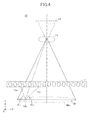
- FIG. 4 is a front view of the image inspection device 10.
- FIG. 5 is a perspective view of an illuminating unit 11 according to the first embodiment. In FIG. 4 , some of the components illustrated in FIG. 3 are omitted for brevity.
- the image inspection device 10 includes the illuminating unit 11 for obtaining the gloss distribution, an illuminating unit 12 for obtaining the density distribution, an imaging lens 13, an image sensor 14, and a feeding unit 15.
- 90 indicates an image-carrying medium such as paper that is to be inspected
- 90a indicates one line of scan area on the image-carrying medium 90
- 90b indicates a feeding direction in which the image-carrying medium 90 is to be fed.
- specular reflection light indicates light reflected from the image-carrying medium 90 at the same angle as the incident angle of illuminating light emitted from the illuminating unit 11, and diffuse reflection light indicates reflected light other than the specular reflection light.
- the illuminating unit 11 includes light-emitting elements 11 1 through 11 16 .
- the light-emitting elements 11 1 through 11 16 emit illuminating lights 11a 1 through 11a 16 that enter the scan area 90a of the image-carrying medium 90 at an incident angle ⁇ 1 .
- 11b 1 through 11b 16 indicate specular reflection lights of the illuminating lights 11a 1 through 11a 16 entering the scan area 90a of the image-carrying medium 90 at the incident angle ⁇ 1 .
- a reflection angle of the specular reflection lights 11b 1 through 11b 16 is the same as the incident angle ⁇ 1 of the illuminating lights 11a 1 through 11a 16 .
- the light-emitting elements 11 1 through 11 16 are directed (or oriented) such that the specular reflection lights 11b 1 through 11b 16 from the scan area 90a of the image-carrying medium 90 enter the pupil of the imaging lens 13. In other words, the illuminating light 11a 1 through the illuminating light 11a 16 emitted from the light-emitting elements 11 1 through 11 16 are not parallel to each other.
- the light-emitting elements 11 1 through 11 16 preferably have high directivity to reduce the emission of light in directions other than the predetermined directions.
- LED light emitting diodes
- EL organic electroluminescence
- the illuminating unit 11 of this embodiment includes 16 light-emitting elements, the number of light-emitting elements is not limited to a specific value. The number of light-emitting elements is preferably large to densely arrange the light-emitting elements along the scan area 90a (in the direction Y in FIGs. 3 and 4 ) and thereby to properly illuminate the scan area 90a so that specular reflection light is obtained from the entire scan area 90a.
- the illuminating unit 11 is an example of a first illuminating unit.
- the illuminating unit 12 emits illuminating light 12a that enters the scan area 90a of the image-carrying medium 90 at a predetermined incident angle.
- the incident angle of the illuminating light 12a may be set at any angle that is different from the incident angle ⁇ 1 .
- the incident angle of the illuminating light 12a may be set at 90 degrees.
- a diffuse illumination device such as a xenon lamp or an LED array may be used.
- the image inspection device 10 is configured to not cause the illuminating unit 11 and the illuminating unit 12 to emit light at the same time.
- the image inspection device 10 may be configured to cause the illuminating unit 11 and the illuminating unit 12 to alternately emit light or to emit light at different timings as needed.
- the illuminating unit 12 is an example of a second illuminating unit.
- the imaging lens 13 and the image sensor 14 are positioned so as to be able to receive the specular reflection lights 11b 1 through 11b 16 . Also, the imaging lens 13 and the image sensor 14 are positioned so as to be able to receive diffuse reflection light 12b that is a part of diffuse reflection light of the illuminating light 12a emitted from the illuminating unit 12 to the scan area 90a of the image-carrying medium 90.
- the imaging lens 13 may include multiple lenses and focuses the specular reflection lights 11b 1 through 11b 16 of the illuminating light 11a 1 through 11a 16 and the diffuse reflection light 12b of the illuminating light 12a on the image sensor 14.
- the imaging lens 13 is an example of a focusing unit.
- the image sensor 14 includes multiple pixels and detects the intensities of the specular reflection lights 11b 1 through 11b 16 and the diffuse reflection light 12b that enter via the imaging lens 13.
- a metal oxide semiconductor (MOS) device a complimentary metal oxide semiconductor (CMOS) device, a charge coupled device (CCD), or a contact image sensor (CIS) may be used as the image sensor 14.
- CMOS complimentary metal oxide semiconductor
- CCD charge coupled device
- CIS contact image sensor
- a one-dimensional image sensor is used as the image sensor 14.
- a three-line image sensor that is sensitive to RGB color components may be used.
- the image sensor 14 is an example of an imaging unit.
- the feeding unit 15 feeds the image-carrying medium 90 in the feeding direction 90b (or in the direction X in FIG. 3 ).
- the image inspection device 10 measures the gloss distribution and the density distribution as described below.
- the image inspection device 10 turns on the illuminating unit 11 (the illuminating unit 12 is turned off) to illuminate the scan area 90a with the illuminating lights 11a 1 through 11a 16 .
- the image sensor 14 detects the intensities of the specular reflection lights 11b 1 through 11b 16 from the scan area 90a.
- the image inspection device 10 inspects the gloss distribution of the scan area 90a based on the intensities of the specular reflection lights 11b 1 through 11b 16 .
- the image inspection device 10 turns on the illuminating unit 12 (the illuminating unit 11 is turned off) to illuminate the scan area 90a with the illuminating light 12a.
- the image sensor 14 detects the intensity of the diffuse reflection light 12b from the scan area 90a. Then, the image inspection device 10 inspects the density distribution of the scan area 90a based on the intensity of the diffuse reflection light 12b. With the above process, the gloss distribution and the density distribution of one line (in one dimension) are obtained.
- the feeding unit 15 feeds the image-carrying medium 90 by a predetermined distance in the feeding direction 90b. Then, the above process is repeated for the next line (in one dimension).
- the image inspection device 10 repeats the above process to inspect the gloss distribution and the density distribution of the image-carrying medium 90 in two dimensions.
- the image inspection device 10 of the first embodiment uses the illuminating unit 11 having high directivity to illuminate the scan area 90a such that specular reflection light from the entire scan area 90a enters the image sensor 14.
- This configuration makes it possible to reduce flare light and thereby makes it possible to accurately inspect the gloss distribution of the image-carrying medium 90.
- the above configuration eliminates the need to provide an extra component such as a half mirror as disclosed in JP2000-123152 . This in turn makes it easier to place the illuminating unit 2 for obtaining the density distribution in a desired position and makes it possible to inspect both the gloss distribution and the density distribution.
- the image inspection device 10 does not include a half mirror, it is possible to efficiently use light emitted from two illuminating units (the illuminating unit 11 and the illuminating unit 12).
- the amount of illuminating light for causing specular reflection light becomes relatively small at the side edges of the scan area 90a and the amount of flare light increases.
- the measured gloss distribution at the side edges of the scan area 90a is affected by the density level of the image-carrying medium 90.
- the first embodiment makes it possible to prevent this problem because the illuminating unit 11 illuminates the scan area 90a such that specular reflection light from the entire scan area 90a (including the side edges) enters the image sensor 14.
- the light-emitting elements 11 1 through 11 16 of the illuminating unit 11 are directed (or oriented) such that the specular reflection lights 11b 1 through 11b 16 from the scan area 90a enter the pupil of the imaging lens 13.
- the illuminating unit 11 is replaced with an illuminating unit 21 and a curved mirror 29 is added.
- the illuminating unit 21 includes light-emitting elements 21 1 through 21 16 that emit illuminating light 21a 1 through illuminating light 21a 16 that are substantially parallel to each other.
- the curved mirror 29 reflects and directs the substantially-parallel illuminating lights 21a 1 through 21a 16 to the scan area 90a such that specular reflection light from the entire scan area 90a enters the pupil of the imaging lens 13.
- Components of the image inspection device 20 other than the illuminating unit 21 and the curved mirror 29 have substantially the same configurations as those of the image inspection device 10, and therefore their descriptions are omitted here.
- FIG. 6 is a side view of the image inspection device 20 according to the first variation of the first embodiment.
- FIG. 7 is a side view of the image inspection device 20.
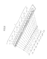
- FIG. 8 is a perspective view of the illuminating unit 21.
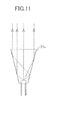
- FIGs. 9 through 11 are cut-away side views of exemplary light-emitting elements of the illuminating unit 21. In FIG. 7 , some of the components illustrated in FIG. 6 are omitted for brevity.
- the image inspection device 20 includes the illuminating unit 21 for obtaining the gloss distribution, the illuminating unit 12 for obtaining the density distribution, the imaging lens 13, the image sensor 14, the feeding unit 15, and the curved mirror 29.
- the light-emitting element 21 n may have a configuration where a lens is formed on an LED (see FIG. 9 ), a configuration where illuminating light from an LED is reflected by a parabolic mirror (see FIG.
- the illuminating unit 21 is formed by arranging the light-emitting elements 21 n in an array with no space between them. With this configuration, the illuminating unit 21 is able to emit substantially-parallel linear light. Accordingly, the illuminating unit 21 can emit substantially-parallel light from its entire light-emitting surface and therefore can continuously (from one end to the other) illuminate the entire scan area 90a.
- the illuminating unit 21 is a parallel linear light source that emits substantially-parallel light from the light-emitting elements 21 1 through 21 16 .
- the illuminating unit 21 of the first variation includes 16 light-emitting elements, the number of light-emitting elements is not limited to a specific value. The number of light-emitting elements is preferably large to densely arrange the light-emitting elements along the scan area 90a (in the direction Y in FIGs. 6 and 7 ) and thereby to evenly illuminate the scan area 90a so that specular reflection light is obtained from the entire scan area 90a.
- the curved mirror 29 has a concave surface having predetermined curvature and extending along the length direction of the illuminating unit 21.
- the curved mirror 29 reflects (or deflects) the substantially-parallel illuminating lights 21a 1 through 21a 16 emitted from the light-emitting elements 21 1 through 21 16 to produce illuminating light 21b 1 through 21b 16 that illuminate the scan area 90a such that resulting specular reflection lights 21c 1 through 21c 16 from the scan area 90a enter the pupil of the imaging lens 13.
- the curvature of the concave surface of the curved mirror 29 is determined such that the specular reflection lights 21c 1 through 21c 16 of the illuminating lights 21b 1 through 21b 16 enter the pupil of the imaging lens 13.
- the illuminating light 21a 1 through the illuminating light 21a 16 emitted from the light-emitting elements 21 1 through 21 16 of the illuminating unit 21 are reflected by the curved mirror 29 in different directions as the illuminating lights 21b 1 through 21b 16 .
- the illuminating lights 21b 1 through 21b 16 enter the entire scan area 90a of the image-carrying medium 90 at an incident angle ⁇ 1 .
- the illuminating lights 21b 1 through 21b 16 are reflected from the entire scan area 90a as the specular reflection lights 21c 1 through 21c 16 .
- the specular reflection lights 21c 1 through 21c 16 enter the pupil of the imaging lens 13.
- the combination of the illuminating unit 21 and the curved mirror 29 is an example of a first illuminating unit.
- the curved mirror 29 is an example of an illuminating light producing unit.
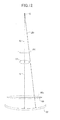
- FIG. 12 is a drawing used to describe the curvature of the curved mirror 29.
- a distance R indicates the sum of the distance from the pupil of the imaging lens 13 to the scan area 90a and the distance from the scan area 90a to the curved mirror 29, and a center of curvature C indicates a position that is apart from the pupil of the imaging lens 13 by the distance R along the optical axis of the imaging lens 13.
- a radius of curvature 29r of the curved mirror 29 is two times greater than the distance R.
- the substantially-parallel illuminating lights 21a 1 through 21a 16 emitted from the light-emitting elements 21 1 through 21 16 are reflected by the curved mirror 29 as the illuminating light 21b 1 through the illuminating light 21b 16 that are not parallel to each other.
- the illuminating lights 21b 1 through 21b 16 illuminate and are reflected by the entire scan area 90a as the specular reflection lights 21c 1 through 21c 16 that enter the pupil of the imaging lens 13.
- the image inspection device 20 of the first variation has advantages similar to those of the image inspection device 10 of the first embodiment and also has advantages as described below.
- the image inspection device 20 of the first variation includes the illuminating unit 21 including the light-emitting elements 21 1 through 21 16 that emit the illuminating light 21a 1 through the illuminating light 21a 16 that are substantially parallel to each other; and the curved mirror 29 that reflects (or deflects) the illuminating lights 21a 1 through 21a 16 to illuminate the entire scan area 90a such that the specular reflection lights 21c 1 through 21c 16 from the entire scan area 90a enter the pupil of the imaging lens 13.
- This configuration makes it possible to substantially eliminate illuminating light that does not produce specular reflection light and to reduce components of light representing flare light, and thereby makes it possible to accurately inspect the gloss distribution.
- the illuminating unit 21 and the curved mirror 29 of the image inspection device 20 can continuously illuminate the scan area 90a of the image-carrying medium 90 in the scanning direction.
- the image inspection device 20 can more accurately inspect the gloss distribution of the image-carrying medium 90.
- the light-emitting elements 21 1 through 21 16 are arranged in a line on a flat substrate.
- the light-emitting elements 21 1 through 21 16 may be arranged in a curved line (to form an arc) so that the illuminating light 21b 1 through the illuminating light 21b 16 are arranged in a line on the image-carrying medium 90 (see FIGs. 13 and 14 ).
- the curvature (or the shape) of the curved line (or the arc) formed by the light-emitting elements 21 1 through 21 16 may be determined according to the curvature of the curved mirror 29.
- the light-emitting elements 21 1 through 21 16 emit illuminating light in a direction that is perpendicular to the printed page.
- the light-emitting elements 11 1 through 11 16 of the illuminating unit 11 are directed (or oriented) such that the specular reflection lights 11b 1 through 11b 16 from the scan area 90a enter the pupil of the imaging lens 13.
- the illuminating unit 11 is replaced with an illuminating unit 31 and a condenser lens 39 is added.
- the illuminating unit 31 includes light-emitting elements 31 1 through 31 16 that emit illuminating light 31a 1 through illuminating light 31a 16 that are substantially parallel to each other.
- the condenser lens 39 causes the substantially-parallel illuminating lights 31a 1 through 31a 16 to illuminate the entire scan area 90a such that specular reflection light from the entire scan area 90a enters the pupil of the imaging lens 13.
- Components of the image inspection device 30 other than the illuminating unit 31 and the condenser lens 39 have substantially the same configurations as those of the image inspection device 10, and therefore their descriptions are omitted here.
- FIG. 15 is a side view of the image inspection device 30 according to the second variation of the first embodiment.
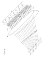
- FIG. 16 is a perspective view of the illuminating unit 31 and the condenser lens 39.
- the image inspection device 30 includes the illuminating unit 31 for obtaining the gloss distribution, the illuminating unit 12 for obtaining the density distribution, the imaging lens 13, the image sensor 14, the feeding unit 15, and the condenser lens 39.
- the reference numbers 31a 2 through 31a 15 are omitted for brevity.
- the light-emitting element 31 n may have a configuration where a lens is formed on an LED (see FIG. 9 ), a configuration where illuminating light from an LED is reflected by a parabolic mirror (see FIG. 10 ), or a configuration where illuminating light from an LED is repeatedly reflected by an inner surface of a horn-shaped (or trumpet-shaped) tube (or cylinder) to form substantially parallel light (see FIG. 11 ).
- the illuminating unit 31 is formed by arranging the light-emitting elements 31 n in an array with no space between them. With this configuration, the illuminating unit 21 is able to emit substantially-parallel linear light.
- the illuminating unit 31 can emit substantially-parallel light from its entire light-emitting surface and therefore can continuously (from one end to the other) illuminate the entire scan area 90a.
- the light-emitting elements 31 n are arranged in a line on a substrate.
- the illuminating unit 31 is a parallel linear light source that emits substantially-parallel light from the light-emitting elements 31 1 through 31 16 .
- the illuminating unit 31 of the second variation includes 16 light-emitting elements, the number of light-emitting elements is not limited to a specific value. The number of light-emitting elements is preferably large to densely arrange the light-emitting elements along the scan area 90a (in the direction Y in FIG. 15 ) and thereby to continuously illuminate the scan area 90a so that specular reflection light is obtained from the entire scan area 90a.
- the condenser lens 39 has convex surfaces having predetermined curvature and extending along the length direction of the illuminating unit 31.
- the condenser lens 39 transmits and deflects the substantially-parallel illuminating lights 31a 1 through 31a 16 emitted from the light-emitting elements 31 1 through 31 16 to produce illuminating lights 31b 1 through 31b 16 that illuminate the scan area 90a such that resulting specular reflection lights 31c 1 through 31c 16 from the scan area 90a enter the pupil of the imaging lens 13.
- the curvature of the convex surfaces of the condenser lens 39 is determined such that the specular reflection lights 31c 1 through 31c 16 of the illuminating lights 31b 1 through 31b 16 enter the pupil of the imaging lens 13. In other words, the focus of the condenser lens 39 is at the pupil of the imaging lens 13.
- the condenser lens 39 is a double-convex lens having two convex surfaces.
- the curvature of each of the convex surfaces is determined such that the focus of the condenser lens 39 corresponds to the pupil of the imaging lens 13.
- any other appropriate lens such as a planoconvex lens or a convex meniscus lens may be used as the condenser lens 39.
- a planoconvex lens is preferably used as the condenser lens 39.
- a double-convex lens is preferably used as the condenser lens 39.
- the illuminating light 31a 1 through the illuminating light 31a 16 emitted from the light-emitting elements 31 1 through 31 16 of the illuminating unit 31 are deflected by the condenser lens 39 in different directions as the illuminating lights 31b 1 through 31b 16 .
- the illuminating lights 31b 1 through 31b 16 enter the entire scan area 90a of the image-carrying medium 90 at an incident angle ⁇ 1 .
- the illuminating lights 31b 1 through 31b 16 are reflected from the entire scan area 90a as the specular reflection lights 31c 1 through 31c 16 .
- the specular reflection lights 31c 1 through 31c 16 enter the pupil of the imaging lens 13.
- the combination of the illuminating unit 31 and the condenser lens 39 is an example of a first illuminating unit.
- the condenser lens 39 is an example of an illuminating light producing unit.
- the image inspection device 30 of the second variation has advantages similar to those of the image inspection device 10 of the first embodiment and also has advantages as described below.
- the image inspection device 30 of the second variation includes the illuminating unit 31 including the light-emitting elements 31 1 through 31 16 that emit the illuminating light 31a 1 through the illuminating light 31a 16 that are substantially parallel to each other; and the condenser lens 39 that deflects the illuminating lights 31a 1 through 31a 16 to illuminate the scan area 90a such that the resulting specular reflection lights 31c 1 through 31c 16 from the entire scan area 90a enter the pupil of the imaging lens 13.
- This configuration makes it possible to substantially eliminate illuminating light that does not produce specular reflection light and to reduce components of light representing flare light, and thereby makes it possible to accurately inspect the gloss distribution.
- the illuminating unit 31 and the condenser lens 39 of the image inspection device 30 can continuously illuminate the scan area 90a of the image-carrying medium 90 in the scanning direction.
- the image inspection device 30 can more accurately inspect the gloss distribution of the image-carrying medium 90.
- the image inspection device 20 of the first variation of the first embodiment uses the curved mirror 29 to deflect (or change the path of) the illuminating light, and the curved mirror 29 can be implemented by a reflection mirror made of an inexpensive material such as high-gloss aluminum. This configuration makes it easier to downsize and reduce the costs of an image inspection device.
- the image inspection device 30 of the second variation of the first embodiment uses the condenser lens 39 that is more expensive than the curved mirror 29.
- the condenser lens 39 can be optimally designed to achieve a desired performance.
- the first embodiment provides the image inspection device 10 that can accurately inspect the gloss distribution of the image-carrying medium 90. Still, there may be a case where the illuminating unit 11 of the image inspection device 10 cannot evenly illuminate the entire scan area 90a.
- a third variation of the first embodiment provides an image inspection device 40 including a blind area processing unit 45 that performs a process in a case where the illuminating unit 11 of the image inspection device 10 cannot evenly illuminate the entire scan area 90a.
- the illuminating unit 11 may not be able to evenly illuminate the entire scan area 90a.
- the blind area processing unit 45 of the image inspection device 40 performs a process related to the blind area.
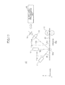
- FIG. 17 is a drawing illustrating the image inspection device 40 according to the third variation of the first embodiment.
- the image inspection device 40 includes the blind area processing unit 45 in addition to the components of the image inspection device 10 of the first embodiment.
- the blind area processing unit 45 includes a CPU and a memory such as a ROM or a RAM that are not shown.
- the memory of the blind area processing unit 45 stores a program for causing the image inspection device 40 to identify a blind area(s) and to prevent the image inspection device 40 from inspecting the gloss of the blind area(s).
- the program is executed by the CPU to implement various functions of the blind area processing unit 45.
- the blind area processing unit 45 identifies blind areas and stores information indicating the identified blind areas in the memory. An exemplary method for identifying blind areas is described below.
- the blind area processing unit 45 causes the feeding unit 15 to feed a specular reflector 95.
- a specular reflector 95 For example, a mirror or a polished metal plate that can specularly reflect illuminating light in its entire area may be used as the specular reflector 95.
- the blind area processing unit 45 causes the illuminating unit 11 to illuminate one line of scan area (scan area 95a) of the specular reflector 95 with the illuminating lights 11a 1 through 11a 16 and causes the image sensor 14 to detect the resulting specular reflection lights 11b 1 through 11b 16 from the scan area 95a.
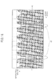
- FIG. 18 is a graph showing exemplary data obtained by scanning the regular reflector 95 with the image sensor 14.
- the horizontal axis indicates the scan area 95a and the vertical axis indicates a detected value detected by the image sensor 14.
- the blind area processing unit 45 compares the detected value with a predetermined threshold 46 and if the detected value of a portion (or a point) of the scan area 95a is less than or equal to the threshold 46, identifies the portion as a blind area 47.
- the blind area processing unit 45 After the above process is completed for one line (in one dimension), the blind area processing unit 45 causes the feeding unit 15 to feed the specular reflector 95 by a predetermined distance in the feeding direction 90b. Then, the blind area processing unit 45 repeats the above process for the next line (in one dimension). Thus, the blind area processing unit 45 repeats the above process to identify blind areas 47 in two dimensions.
- the blind area processing unit 45 obtains gloss data indicating the gloss of the image-carrying medium 90 that is fed by the feeding unit 15.
- the blind area processing unit 45 removes data corresponding to the blind areas 47 from the gloss data obtained in the second step.
- the blind area processing unit 45 obtains "effective" gloss data not including data corresponding to the blind areas 47 through the first through third steps described above.
- the blind area processing unit 45 may be configured to not obtain gloss data of the blind areas 47 instead of removing the data corresponding to the blind areas 47 from the gloss data of the entire image-carrying medium 90.
- the image inspection device 40 of the third variation has advantages similar to those of the image inspection device 10 of the first embodiment and also has advantages as described below.
- the image inspection device 40 including the blind area processing unit 45 makes it possible to accurately inspect the gloss distribution by excluding gloss data corresponding to the blind areas 47 even when the illuminating unit 11 cannot evenly illuminate the entire scan area 90a.
- FIG. 19 is a schematic diagram of an image forming apparatus 80 according to the second embodiment.
- the image forming apparatus 80 includes the image inspection device 10, a paper-feed cassette 81a, a paper-feed cassette 81b, paper feeding rollers 82, a controller 83, an optical scanning system 84, photoconductors 85, an intermediate transfer part 86, fusing rollers 87, and paper ejecting rollers 88.
- 90 indicates an image-carrying medium such as paper.
- the image-carrying medium 90 is fed from the paper-feed cassette 81a or 81b via a guide and the paper feeding rollers 82 to the intermediate transfer part 86.
- the photoconductors 85 are exposed by the optical scanning system 84 to form latent images and the latent images are developed with color materials (e.g., toner).
- the developed images are transferred onto and superposed on the intermediate transfer part 86, and the superposed image is transferred from the intermediate transfer part 86 onto the image-carrying medium 90.
- the superposed image on the image-carrying medium 90 is fused by the fusing rollers 87 and the image-carry medium 90 with the fused image is ejected by the ejecting rollers 88.
- the image inspection device 10 is disposed downstream of the fusing rollers 87.
- the image inspection device 10 is disposed in a predetermined position to inspect the gloss distribution as well as the density distribution of the image-carrying medium 90.
- the inspection results of the gloss distribution and the density distribution may be fed back, for example, to the controller 83 to improve the quality of an image to be formed on the image-carrying medium 90.
- the image inspection device 10 of the image forming apparatus 80 may be replaced with the image inspection device 20, 30, or 40.
Landscapes
- Life Sciences & Earth Sciences (AREA)
- Biochemistry (AREA)
- Immunology (AREA)
- Pathology (AREA)
- Physics & Mathematics (AREA)
- Health & Medical Sciences (AREA)
- Chemical & Material Sciences (AREA)
- Textile Engineering (AREA)
- General Health & Medical Sciences (AREA)
- Analytical Chemistry (AREA)
- General Physics & Mathematics (AREA)
- Engineering & Computer Science (AREA)
- Wood Science & Technology (AREA)
- Investigating Materials By The Use Of Optical Means Adapted For Particular Applications (AREA)
- Inking, Control Or Cleaning Of Printing Machines (AREA)
- Image Input (AREA)
Abstract
Description
- A certain aspect of this disclosure relates to an image inspection device and an image forming apparatus.
- In an electrophotographic image forming apparatus, a toner image formed on paper is fused onto the paper by a fusing unit. Therefore, normally, the gloss of the paper (or the image) depends on the amount of toner adhering to the paper. However, even when a toner image is accurately formed on paper (or the distribution of the amount of toner is accurately represented on the paper), the toner image may be unevenly fused onto the paper due to, for example, a problem of a fusing unit of an image forming apparatus and the unevenness in the fusing often results in stripes on the fused toner image.
- Even when a toner image is unevenly fused, the image density distribution of the toner image may not be affected. However, stripes resulting from the variation in gloss may be observed on the toner image from oblique directions. The stripes represent image defects and are called "fuser stripes". Meanwhile, when an electrophotographic image forming apparatus is used as a digital printing press, it is often necessary to improve the gloss of an output image by, for example, applying transparent toner to the output image or using high gloss paper.
- For the above reasons, there is a demand for an image inspection device than can inspect an image output from an electrophotographic image forming apparatus on demand. Such an image inspection device preferably includes a function for measuring the gloss distribution in the entire area of an output image in addition to a function for measuring the density distribution of the output image. The gloss of an object is measured, for example, by illuminating the object at a predetermined illuminating angle and by measuring the intensity of specular reflection light from the object. In this case, the incident angle and the reflection angle of the light are the same, i.e., they are the same as the illuminating angle, and the illuminating angle is determined depending on the object.
- Meanwhile, images to be inspected by an image inspection device may be formed on various types of paper. To reduce the variation in measurements resulting from the difference in the type of paper, a reduction optical system is more preferably used than a 1X optical system to scan an image. This is because the scan resolution and the focus of a 1X optical system change depending on the imaging distance that varies according to the thickness of paper. Meanwhile, the influence of the thickness of paper on a reduction optical system is less significant.
- Here, if a contact glass is provided between an imaging system and an output image when optically detecting the gloss distribution of the output image, the detection results are greatly influenced by a gloss component of the surface reflection light from the contact glass. Therefore, it is not preferable to use a contact glass to make the imaging distance constant. This also makes it difficult to use a 1X optical system for an image inspection device.
- Technologies for measuring the gloss distribution of an output image are disclosed, for example, in Japanese Laid-Open Patent Publication No.
2006-284550 2000-123152 - In an aspect of this disclosure, there is provided a device for inspecting an image formed on an object. The device includes a first illuminating unit illuminating the object from an oblique direction with a first illuminating light; an imaging unit receiving specular reflection light of the first illuminating light from the object; and a focusing unit focusing the specular reflection light on the imaging unit. The device is configured to inspect the image based on intensity of the specular reflection light received by the imaging unit. The first illuminating unit includes light-emitting elements and an illumination light producing unit that is configured to deflect light emitted from the light-emitting elements and thereby to produce the first illuminating light such that the specular reflection light from the object enters a pupil of the focusing unit.
- In another aspect of this disclosure, there is provided a device for inspecting an image formed on an object. The device includes a first illuminating unit illuminating the object from an oblique direction with a first illuminating light; an imaging unit receiving specular reflection light of the first illuminating light from the object; and a focusing unit focusing the specular reflection light on the imaging unit. The device is configured to inspect the image based on intensity of the specular reflection light received by the imaging unit. The first illuminating unit includes light-emitting elements that are directed such that the specular reflection light from the object enters a pupil of the focusing unit.
-
-
FIG. 1 is a side view of a related-art image inspection device; -
FIG. 2 is a front view of the related-art image inspection device ofFIG. 1 ; -
FIG. 3 is a side view of an image inspection device according to a first embodiment; -
FIG. 4 is a front view of the image inspection device according to the first embodiment; -
FIG. 5 is a perspective view of an illuminating unit according to the first embodiment; -
FIG. 6 is a side view of an image inspection device according to a first variation of the first embodiment; -
FIG. 7 is a front view of the image inspection device according to the first variation of the first embodiment; -
FIG. 8 is a perspective view of an illuminating unit according to the first variation of the first embodiment; -
FIG. 9 is a cut-away side view (1) of a light-emitting element of the illuminating unit according to the first variation of the first embodiment; -
FIG. 10 is a cut-away side view (2) of a light-emitting element of the illuminating unit according to the first variation of the first embodiment; -
FIG. 11 is a cut-away side view (3) of a light-emitting element of the illuminating unit according to the first variation of the first embodiment; -
FIG. 12 is a drawing used to describe curvature of a curved mirror; -
FIG. 13 is a plan view of an array of light-emitting elements of the illuminating unit according to the first variation of the first embodiment; -
FIG. 14 is a front view of the array of light-emitting elements of the illuminating unit according to the first variation of the first embodiment; -
FIG. 15 is a side view of an image inspection device according to a second variation of the first embodiment; -
FIG. 16 is a perspective view of an illuminating unit and a condenser lens according to the second variation of the first embodiment; -
FIG. 17 is a drawing illustrating an image inspection device according to a third variation of the first embodiment; -
FIG. 18 is a graph showing exemplary data obtained by scanning a regular reflector with an image sensor; and -
FIG. 19 is a schematic diagram of an image forming apparatus according to a second embodiment. - With the technology disclosed in
JP2006-284550 JP2006-284550 - With the technology disclosed in
JP2000-123152 FIGs. 1 and2 , with the technology disclosed inJP2000-123152 line light source 3 for specular reflection is reflected by ahalf mirror 4 and reaches a printedmatter 5. Then, specular reflection light from the printedmatter 5 passes through thehalf mirror 4 and enters acamera 1. In this process, the intensity of the illuminating light is reduced to one half by thehalf mirror 4 and the specular reflection light is also reduced to one half by thehalf mirror 4. - With this configuration, as illustrated in
FIG. 2 , the side edges of the printedmatter 5 need to be illuminated by edge-illuminating light 6 emitted from the ends of theline light source 3 to obtain specular reflection light from the side edges of the printedmatter 5. Accordingly, the width of theline light source 3 needs to be far greater than the width of the printedmatter 5. It is possible to reduce the width of the linelight source 3 by positioning thehalf mirror 4 as close as possible to the printedmatter 5. In this case, however, thehalf mirror 4 interferes with a linelight source 2 for diffuse reflection. - Also, since the illuminating light emitted from the line
light source 3 is not directional, the side edges of the printedmatter 5 are also illuminated from directions other than the direction of theedge illuminating light 6. As a result, reflected light (diffuse reflection light of illuminating light from the other directions) other than the specular reflection light of the edge illuminating light 6 also enters thecamera 1. This makes it difficult to accurately measure the gloss distribution. - Also, since the
half mirror 4 is used inJP2000-123152 light source 2 for diffuse reflection is reduced to one half and the intensity of light from the linelight source 3 for specular reflection is reduced to one fourth. Thus, with the configuration ofJP2000-123152 JP2000-123152 light source 3 illuminates the printedmatter 5 via thehalf mirror 4 such that the optical axis of the illuminating light matches the optical axis of thecamera 1", but does not provide specific examples or embodiments to implement this feature. - Thus, with the related-art technologies, it is difficult to obtain an accurate gloss distribution of the entire area of an object.
- An aspect of this disclosure provides an image inspection device that can accurately measure the gloss distribution of the entire area of an object, and an image forming apparatus including the image inspection device.
- Preferred embodiments of the present invention are described below with reference to the accompanying drawings. Throughout the accompanying drawings, the same reference numbers are used for the same components, and overlapping descriptions of those components are omitted.
-
FIG. 3 is a side view of animage inspection device 10 according to a first embodiment.FIG. 4 is a front view of theimage inspection device 10.FIG. 5 is a perspective view of an illuminatingunit 11 according to the first embodiment. InFIG. 4 , some of the components illustrated inFIG. 3 are omitted for brevity. - Referring to
FIGs. 3 ,4 , and5 , theimage inspection device 10 includes the illuminatingunit 11 for obtaining the gloss distribution, an illuminatingunit 12 for obtaining the density distribution, animaging lens 13, animage sensor 14, and afeeding unit 15. Also inFIGs. 3 and4 , 90 indicates an image-carrying medium such as paper that is to be inspected, 90a indicates one line of scan area on the image-carryingmedium medium 90 is to be fed. - In the descriptions below, specular reflection light indicates light reflected from the image-carrying
medium 90 at the same angle as the incident angle of illuminating light emitted from the illuminatingunit 11, and diffuse reflection light indicates reflected light other than the specular reflection light. - The illuminating
unit 11 includes light-emittingelements 111 through 1116. The light-emittingelements 111 through 1116 emit illuminating lights 11a1 through 11a16 that enter thescan area 90a of the image-carryingmedium 90 at an incident angle θ1. InFIG. 3 , 11b1 through 11b16 indicate specular reflection lights of the illuminating lights 11a1 through 11a16 entering thescan area 90a of the image-carryingmedium 90 at the incident angle θ1. A reflection angle of the specular reflection lights 11b1 through 11b16 is the same as the incident angle θ1 of the illuminating lights 11a1 through 11a16. The light-emittingelements 111 through 1116 are directed (or oriented) such that the specular reflection lights 11b1 through 11b16 from thescan area 90a of the image-carryingmedium 90 enter the pupil of theimaging lens 13. In other words, the illuminating light 11a1 through the illuminating light 11a16 emitted from the light-emittingelements 111 through 1116 are not parallel to each other. - The light-emitting
elements 111 through 1116 preferably have high directivity to reduce the emission of light in directions other than the predetermined directions. An image formed in thescan area 90a of the image-carryingmedium 90 has an image density distribution in addition to a gloss distribution. Assuming that aportion 90x of thescan area 90a is to be illuminated by illuminating light 11an (n=1-16) and flare light 19 indicates light from an unintended direction, a part of diffuse reflection light corresponding to the image density of theportion 90x illuminated by theflare light 19 enters theimage sensor 14. As a result, the part of the diffuse reflection light is detected as a gloss component and reduces the inspection accuracy. - Thus, if the directivity of light-emitting elements is low, flare light (or illuminating light from an unintended direction) is produced and the inspection accuracy is reduced as in the related-art example illustrated in
FIGs. 1 and2 . In this embodiment, highly-directional light-emitting elements are used as the light-emittingelements 111 through 1116 to reduce flare light and to improve the inspection accuracy. - For example, light emitting diodes (LED) or organic electroluminescence (EL) elements may be used as the light-emitting
elements 111 through 1116. Compared with a fluorescent lamp, an LED has high light-emitting directivity and is therefore preferable for the illuminatingunit 11. Although the illuminatingunit 11 of this embodiment includes 16 light-emitting elements, the number of light-emitting elements is not limited to a specific value. The number of light-emitting elements is preferably large to densely arrange the light-emitting elements along thescan area 90a (in the direction Y inFIGs. 3 and4 ) and thereby to properly illuminate thescan area 90a so that specular reflection light is obtained from theentire scan area 90a. - The illuminating
unit 11 is an example of a first illuminating unit. - The illuminating
unit 12 emits illuminating light 12a that enters thescan area 90a of the image-carryingmedium 90 at a predetermined incident angle. The incident angle of the illuminating light 12a may be set at any angle that is different from the incident angle θ 1. For example, the incident angle of the illuminating light 12a may be set at 90 degrees. As the illuminating light 12a, for example, a diffuse illumination device such as a xenon lamp or an LED array may be used. Theimage inspection device 10 is configured to not cause the illuminatingunit 11 and the illuminatingunit 12 to emit light at the same time. For example, theimage inspection device 10 may be configured to cause the illuminatingunit 11 and the illuminatingunit 12 to alternately emit light or to emit light at different timings as needed. The illuminatingunit 12 is an example of a second illuminating unit. - The
imaging lens 13 and theimage sensor 14 are positioned so as to be able to receive the specular reflection lights 11b1 through 11b16. Also, theimaging lens 13 and theimage sensor 14 are positioned so as to be able to receive diffuse reflection light 12b that is a part of diffuse reflection light of the illuminating light 12a emitted from the illuminatingunit 12 to thescan area 90a of the image-carryingmedium 90. Theimaging lens 13 may include multiple lenses and focuses the specular reflection lights 11b1 through 11b16 of the illuminating light 11a1 through 11a16 and the diffuse reflection light 12b of the illuminating light 12a on theimage sensor 14. Theimaging lens 13 is an example of a focusing unit. - The
image sensor 14 includes multiple pixels and detects the intensities of the specular reflection lights 11b1 through 11b16 and the diffuse reflection light 12b that enter via theimaging lens 13. For example, a metal oxide semiconductor (MOS) device, a complimentary metal oxide semiconductor (CMOS) device, a charge coupled device (CCD), or a contact image sensor (CIS) may be used as theimage sensor 14. In this embodiment, a one-dimensional image sensor is used as theimage sensor 14. When a color image is to be inspected, a three-line image sensor that is sensitive to RGB color components may be used. Theimage sensor 14 is an example of an imaging unit. - The
feeding unit 15 feeds the image-carryingmedium 90 in thefeeding direction 90b (or in the direction X inFIG. 3 ). - The
image inspection device 10 measures the gloss distribution and the density distribution as described below. Theimage inspection device 10 turns on the illuminating unit 11 (the illuminatingunit 12 is turned off) to illuminate thescan area 90a with the illuminating lights 11a1 through 11a16. Theimage sensor 14 detects the intensities of the specular reflection lights 11b1 through 11b16 from thescan area 90a. Then, theimage inspection device 10 inspects the gloss distribution of thescan area 90a based on the intensities of the specular reflection lights 11b1 through 11b16. Next, theimage inspection device 10 turns on the illuminating unit 12 (the illuminatingunit 11 is turned off) to illuminate thescan area 90a with the illuminating light 12a. Theimage sensor 14 detects the intensity of the diffuse reflection light 12b from thescan area 90a. Then, theimage inspection device 10 inspects the density distribution of thescan area 90a based on the intensity of the diffuse reflection light 12b. With the above process, the gloss distribution and the density distribution of one line (in one dimension) are obtained. - After the inspection of the gloss distribution and the density distribution of one line (in one dimension) is completed, the
feeding unit 15 feeds the image-carryingmedium 90 by a predetermined distance in thefeeding direction 90b. Then, the above process is repeated for the next line (in one dimension). Thus, theimage inspection device 10 repeats the above process to inspect the gloss distribution and the density distribution of the image-carryingmedium 90 in two dimensions. - As described above, the
image inspection device 10 of the first embodiment uses the illuminatingunit 11 having high directivity to illuminate thescan area 90a such that specular reflection light from theentire scan area 90a enters theimage sensor 14. This configuration makes it possible to reduce flare light and thereby makes it possible to accurately inspect the gloss distribution of the image-carryingmedium 90. Also, the above configuration eliminates the need to provide an extra component such as a half mirror as disclosed inJP2000-123152 unit 2 for obtaining the density distribution in a desired position and makes it possible to inspect both the gloss distribution and the density distribution. Further, since theimage inspection device 10 does not include a half mirror, it is possible to efficiently use light emitted from two illuminating units (the illuminatingunit 11 and the illuminating unit 12). - If a diffuse illumination device such as a fluorescent lamp is used as in the related art, the amount of illuminating light for causing specular reflection light becomes relatively small at the side edges of the
scan area 90a and the amount of flare light increases. As a result, the measured gloss distribution at the side edges of thescan area 90a is affected by the density level of the image-carryingmedium 90. The first embodiment makes it possible to prevent this problem because the illuminatingunit 11 illuminates thescan area 90a such that specular reflection light from theentire scan area 90a (including the side edges) enters theimage sensor 14. - In the
image inspection device 10 of the first embodiment, the light-emittingelements 111 through 1116 of the illuminatingunit 11 are directed (or oriented) such that the specular reflection lights 11b1 through 11b16 from thescan area 90a enter the pupil of theimaging lens 13. In animage inspection device 20 of the first variation, the illuminatingunit 11 is replaced with an illuminatingunit 21 and acurved mirror 29 is added. The illuminatingunit 21 includes light-emittingelements 211 through 2116 that emit illuminating light 21a1 through illuminating light 21a16 that are substantially parallel to each other. Thecurved mirror 29 reflects and directs the substantially-parallel illuminating lights 21a1 through 21a16 to thescan area 90a such that specular reflection light from theentire scan area 90a enters the pupil of theimaging lens 13. Components of theimage inspection device 20 other than the illuminatingunit 21 and thecurved mirror 29 have substantially the same configurations as those of theimage inspection device 10, and therefore their descriptions are omitted here. -
FIG. 6 is a side view of theimage inspection device 20 according to the first variation of the first embodiment.FIG. 7 is a side view of theimage inspection device 20.FIG. 8 is a perspective view of the illuminatingunit 21.FIGs. 9 through 11 are cut-away side views of exemplary light-emitting elements of the illuminatingunit 21. InFIG. 7 , some of the components illustrated inFIG. 6 are omitted for brevity. - Referring to
FIGs. 6 through 11 , theimage inspection device 20 includes the illuminatingunit 21 for obtaining the gloss distribution, the illuminatingunit 12 for obtaining the density distribution, theimaging lens 13, theimage sensor 14, thefeeding unit 15, and thecurved mirror 29. - The light-emitting
elements 211 through 2116 (may be represented by "light-emittingelement 21n", n= 1-16) of the illuminatingunit 21 emit the illuminating light 21a1 through the illuminating light 21a16 that are substantially parallel to each other and enter thecurved mirror 29. For example, the light-emittingelement 21n may have a configuration where a lens is formed on an LED (seeFIG. 9 ), a configuration where illuminating light from an LED is reflected by a parabolic mirror (seeFIG. 10 ), or a configuration where illuminating light from an LED is repeatedly reflected by an inner surface of a horn-shaped (or trumpet-shaped) tube (or cylinder) to form substantially-parallel light (seeFIG. 11 ). The illuminatingunit 21 is formed by arranging the light-emittingelements 21n in an array with no space between them. With this configuration, the illuminatingunit 21 is able to emit substantially-parallel linear light. Accordingly, the illuminatingunit 21 can emit substantially-parallel light from its entire light-emitting surface and therefore can continuously (from one end to the other) illuminate theentire scan area 90a. - Thus, the illuminating
unit 21 is a parallel linear light source that emits substantially-parallel light from the light-emittingelements 211 through 2116. Although the illuminatingunit 21 of the first variation includes 16 light-emitting elements, the number of light-emitting elements is not limited to a specific value. The number of light-emitting elements is preferably large to densely arrange the light-emitting elements along thescan area 90a (in the direction Y inFIGs. 6 and7 ) and thereby to evenly illuminate thescan area 90a so that specular reflection light is obtained from theentire scan area 90a. - The
curved mirror 29 has a concave surface having predetermined curvature and extending along the length direction of the illuminatingunit 21. Thecurved mirror 29 reflects (or deflects) the substantially-parallel illuminating lights 21a1 through 21a16 emitted from the light-emittingelements 211 through 2116 to produce illuminating light 21b1 through 21b16 that illuminate thescan area 90a such that resulting specular reflection lights 21c1 through 21c16 from thescan area 90a enter the pupil of theimaging lens 13. The curvature of the concave surface of thecurved mirror 29 is determined such that the specular reflection lights 21c1 through 21c16 of the illuminating lights 21b1 through 21b16 enter the pupil of theimaging lens 13. - The illuminating light 21a1 through the illuminating light 21a16 emitted from the light-emitting
elements 211 through 2116 of the illuminatingunit 21 are reflected by thecurved mirror 29 in different directions as the illuminating lights 21b1 through 21b16. The illuminating lights 21b1 through 21b16 enter theentire scan area 90a of the image-carryingmedium 90 at an incident angle θ1. Then, the illuminating lights 21b1 through 21b16 are reflected from theentire scan area 90a as the specular reflection lights 21c1 through 21c16. Then, the specular reflection lights 21c1 through 21c16 enter the pupil of theimaging lens 13. The combination of the illuminatingunit 21 and thecurved mirror 29 is an example of a first illuminating unit. Also, thecurved mirror 29 is an example of an illuminating light producing unit. - The curvature of the
curved mirror 29 is described below with reference toFIG. 12. FIG. 12 is a drawing used to describe the curvature of thecurved mirror 29. InFIG. 12 , a distance R indicates the sum of the distance from the pupil of theimaging lens 13 to thescan area 90a and the distance from thescan area 90a to thecurved mirror 29, and a center of curvature C indicates a position that is apart from the pupil of theimaging lens 13 by the distance R along the optical axis of theimaging lens 13. As illustrated inFIG. 12 , a radius of curvature 29r of thecurved mirror 29 is two times greater than the distance R. With this configuration, the substantially-parallel illuminating lights 21a1 through 21a16 emitted from the light-emittingelements 211 through 2116 are reflected by thecurved mirror 29 as the illuminating light 21b1 through the illuminating light 21b16 that are not parallel to each other. The illuminating lights 21b1 through 21b16 illuminate and are reflected by theentire scan area 90a as the specular reflection lights 21c1 through 21c16 that enter the pupil of theimaging lens 13. - The
image inspection device 20 of the first variation has advantages similar to those of theimage inspection device 10 of the first embodiment and also has advantages as described below. As described above, theimage inspection device 20 of the first variation includes the illuminatingunit 21 including the light-emittingelements 211 through 2116 that emit the illuminating light 21a1 through the illuminating light 21a16 that are substantially parallel to each other; and thecurved mirror 29 that reflects (or deflects) the illuminating lights 21a1 through 21a16 to illuminate theentire scan area 90a such that the specular reflection lights 21c1 through 21c16 from theentire scan area 90a enter the pupil of theimaging lens 13. This configuration makes it possible to substantially eliminate illuminating light that does not produce specular reflection light and to reduce components of light representing flare light, and thereby makes it possible to accurately inspect the gloss distribution. - Compared with the illuminating
unit 11 of theimage inspection device 10, the illuminatingunit 21 and thecurved mirror 29 of theimage inspection device 20 can continuously illuminate thescan area 90a of the image-carryingmedium 90 in the scanning direction. Thus, theimage inspection device 20 can more accurately inspect the gloss distribution of the image-carryingmedium 90. - In
FIG. 8 , the light-emittingelements 211 through 2116 are arranged in a line on a flat substrate. Alternatively, the light-emittingelements 211 through 2116 may be arranged in a curved line (to form an arc) so that the illuminating light 21b1 through the illuminating light 21b16 are arranged in a line on the image-carrying medium 90 (seeFIGs. 13 and 14 ). The curvature (or the shape) of the curved line (or the arc) formed by the light-emittingelements 211 through 2116 may be determined according to the curvature of thecurved mirror 29. InFIG. 14 , the light-emittingelements 211 through 2116 emit illuminating light in a direction that is perpendicular to the printed page. - In the
image inspection device 10 of the first embodiment, the light-emittingelements 111 through 1116 of the illuminatingunit 11 are directed (or oriented) such that the specular reflection lights 11b1 through 11b16 from thescan area 90a enter the pupil of theimaging lens 13. In animage inspection device 30 of the second variation, the illuminatingunit 11 is replaced with an illuminatingunit 31 and acondenser lens 39 is added. The illuminatingunit 31 includes light-emittingelements 311 through 3116 that emit illuminating light 31a1 through illuminating light 31a16 that are substantially parallel to each other. Thecondenser lens 39 causes the substantially-parallel illuminating lights 31a1 through 31a16 to illuminate theentire scan area 90a such that specular reflection light from theentire scan area 90a enters the pupil of theimaging lens 13. Components of theimage inspection device 30 other than the illuminatingunit 31 and thecondenser lens 39 have substantially the same configurations as those of theimage inspection device 10, and therefore their descriptions are omitted here. -
FIG. 15 is a side view of theimage inspection device 30 according to the second variation of the first embodiment.FIG. 16 is a perspective view of the illuminatingunit 31 and thecondenser lens 39. Referring toFIGs. 15 and16 , theimage inspection device 30 includes the illuminatingunit 31 for obtaining the gloss distribution, the illuminatingunit 12 for obtaining the density distribution, theimaging lens 13, theimage sensor 14, thefeeding unit 15, and thecondenser lens 39. - The light-emitting
elements 311 through 3116 (may be represented by "light-emittingelement 31n", n= 1-16) of the illuminatingunit 31 emit the illuminating light 31a1 through the illuminating light 31a16 that are substantially parallel to each other and enter thecondenser lens 39. InFIG. 16 , the reference numbers 31a2 through 31a15 are omitted for brevity. - For example, the light-emitting
element 31n may have a configuration where a lens is formed on an LED (seeFIG. 9 ), a configuration where illuminating light from an LED is reflected by a parabolic mirror (seeFIG. 10 ), or a configuration where illuminating light from an LED is repeatedly reflected by an inner surface of a horn-shaped (or trumpet-shaped) tube (or cylinder) to form substantially parallel light (seeFIG. 11 ). The illuminatingunit 31 is formed by arranging the light-emittingelements 31n in an array with no space between them. With this configuration, the illuminatingunit 21 is able to emit substantially-parallel linear light. Accordingly, the illuminatingunit 31 can emit substantially-parallel light from its entire light-emitting surface and therefore can continuously (from one end to the other) illuminate theentire scan area 90a. The light-emittingelements 31n are arranged in a line on a substrate. - Thus, the illuminating
unit 31 is a parallel linear light source that emits substantially-parallel light from the light-emittingelements 311 through 3116. Although the illuminatingunit 31 of the second variation includes 16 light-emitting elements, the number of light-emitting elements is not limited to a specific value. The number of light-emitting elements is preferably large to densely arrange the light-emitting elements along thescan area 90a (in the direction Y inFIG. 15 ) and thereby to continuously illuminate thescan area 90a so that specular reflection light is obtained from theentire scan area 90a. - The
condenser lens 39 has convex surfaces having predetermined curvature and extending along the length direction of the illuminatingunit 31. Thecondenser lens 39 transmits and deflects the substantially-parallel illuminating lights 31a1 through 31a16 emitted from the light-emittingelements 311 through 3116 to produce illuminatinglights 31b1 through 31b16 that illuminate thescan area 90a such that resulting specular reflection lights 31c1 through 31c16 from thescan area 90a enter the pupil of theimaging lens 13. The curvature of the convex surfaces of thecondenser lens 39 is determined such that the specular reflection lights 31c1 through 31c16 of the illuminatinglights 31b1 through 31b16 enter the pupil of theimaging lens 13. In other words, the focus of thecondenser lens 39 is at the pupil of theimaging lens 13. - In the example illustrated in
FIG. 16 , thecondenser lens 39 is a double-convex lens having two convex surfaces. The curvature of each of the convex surfaces is determined such that the focus of thecondenser lens 39 corresponds to the pupil of theimaging lens 13. Alternatively, any other appropriate lens such as a planoconvex lens or a convex meniscus lens may be used as thecondenser lens 39. When monochromatic light is used as the illuminating light, the influence of chromatic aberration is small and therefore a planoconvex lens is preferably used as thecondenser lens 39. Meanwhile, to achieve desired curvature with an inexpensive material having a low refractive index, a double-convex lens is preferably used as thecondenser lens 39. - The illuminating light 31a1 through the illuminating light 31a16 emitted from the light-emitting
elements 311 through 3116 of the illuminatingunit 31 are deflected by thecondenser lens 39 in different directions as the illuminatinglights 31b1 through 31b16. The illuminating lights 31b1 through 31b16 enter theentire scan area 90a of the image-carryingmedium 90 at an incident angle θ1. Then, the illuminatinglights 31b1 through 31b16 are reflected from theentire scan area 90a as the specular reflection lights 31c1 through 31c16. Then, the specular reflection lights 31c1 through 31c16 enter the pupil of theimaging lens 13. The combination of the illuminatingunit 31 and thecondenser lens 39 is an example of a first illuminating unit. Also, thecondenser lens 39 is an example of an illuminating light producing unit. - The
image inspection device 30 of the second variation has advantages similar to those of theimage inspection device 10 of the first embodiment and also has advantages as described below. As described above, theimage inspection device 30 of the second variation includes the illuminatingunit 31 including the light-emittingelements 311 through 3116 that emit the illuminating light 31a1 through the illuminating light 31a16 that are substantially parallel to each other; and thecondenser lens 39 that deflects the illuminating lights 31a1 through 31a16 to illuminate thescan area 90a such that the resulting specular reflection lights 31c1 through 31c16 from theentire scan area 90a enter the pupil of theimaging lens 13. This configuration makes it possible to substantially eliminate illuminating light that does not produce specular reflection light and to reduce components of light representing flare light, and thereby makes it possible to accurately inspect the gloss distribution. - Compared with the illuminating
unit 11 of theimage inspection device 10, the illuminatingunit 31 and thecondenser lens 39 of theimage inspection device 30 can continuously illuminate thescan area 90a of the image-carryingmedium 90 in the scanning direction. Thus, theimage inspection device 30 can more accurately inspect the gloss distribution of the image-carryingmedium 90. - The
image inspection device 20 of the first variation of the first embodiment uses thecurved mirror 29 to deflect (or change the path of) the illuminating light, and thecurved mirror 29 can be implemented by a reflection mirror made of an inexpensive material such as high-gloss aluminum. This configuration makes it easier to downsize and reduce the costs of an image inspection device. Meanwhile, theimage inspection device 30 of the second variation of the first embodiment uses thecondenser lens 39 that is more expensive than thecurved mirror 29. However, unlike a free-form surface that is formed by bending a material, thecondenser lens 39 can be optimally designed to achieve a desired performance. - The first embodiment provides the
image inspection device 10 that can accurately inspect the gloss distribution of the image-carryingmedium 90. Still, there may be a case where the illuminatingunit 11 of theimage inspection device 10 cannot evenly illuminate theentire scan area 90a. A third variation of the first embodiment provides animage inspection device 40 including a blindarea processing unit 45 that performs a process in a case where the illuminatingunit 11 of theimage inspection device 10 cannot evenly illuminate theentire scan area 90a. - For example, if there is a gap between the light-emitting
elements 111 through 1116 or if the effective light-emitting surface of the light-emittingelements 111 through 1116 is smaller than their size, the illuminatingunit 11 may not be able to evenly illuminate theentire scan area 90a. In such a case, there is a portion in thescan area 90a which is not illuminated by any one of the illuminating light 11a1 through the illuminating light 11a16. This portion is called a blind area where specular reflection light is not produced and the gloss cannot be measured. The blindarea processing unit 45 of theimage inspection device 40 performs a process related to the blind area. -
FIG. 17 is a drawing illustrating theimage inspection device 40 according to the third variation of the first embodiment. As illustrated inFIG. 17 , theimage inspection device 40 includes the blindarea processing unit 45 in addition to the components of theimage inspection device 10 of the first embodiment. The blindarea processing unit 45 includes a CPU and a memory such as a ROM or a RAM that are not shown. The memory of the blindarea processing unit 45 stores a program for causing theimage inspection device 40 to identify a blind area(s) and to prevent theimage inspection device 40 from inspecting the gloss of the blind area(s). The program is executed by the CPU to implement various functions of the blindarea processing unit 45. - An exemplary process performed by the blind
area processing unit 45 is described below. In a first step, the blindarea processing unit 45 identifies blind areas and stores information indicating the identified blind areas in the memory. An exemplary method for identifying blind areas is described below. First, the blindarea processing unit 45 causes thefeeding unit 15 to feed aspecular reflector 95. For example, a mirror or a polished metal plate that can specularly reflect illuminating light in its entire area may be used as thespecular reflector 95. Next, the blindarea processing unit 45 causes the illuminatingunit 11 to illuminate one line of scan area (scanarea 95a) of thespecular reflector 95 with the illuminating lights 11a1 through 11a16 and causes theimage sensor 14 to detect the resulting specular reflection lights 11b1 through 11b16 from thescan area 95a. -
FIG. 18 is a graph showing exemplary data obtained by scanning theregular reflector 95 with theimage sensor 14. InFIG. 18 , the horizontal axis indicates thescan area 95a and the vertical axis indicates a detected value detected by theimage sensor 14. As the intensity of light entering theimage sensor 14 increases, the detected value increases (i.e., the position of the detected value in the graph becomes higher). The blindarea processing unit 45 compares the detected value with a predetermined threshold 46 and if the detected value of a portion (or a point) of thescan area 95a is less than or equal to the threshold 46, identifies the portion as ablind area 47. After the above process is completed for one line (in one dimension), the blindarea processing unit 45 causes thefeeding unit 15 to feed thespecular reflector 95 by a predetermined distance in thefeeding direction 90b. Then, the blindarea processing unit 45 repeats the above process for the next line (in one dimension). Thus, the blindarea processing unit 45 repeats the above process to identifyblind areas 47 in two dimensions. - In a second step, the blind
area processing unit 45 obtains gloss data indicating the gloss of the image-carryingmedium 90 that is fed by thefeeding unit 15. In a third step, the blindarea processing unit 45 removes data corresponding to theblind areas 47 from the gloss data obtained in the second step. Thus, the blindarea processing unit 45 obtains "effective" gloss data not including data corresponding to theblind areas 47 through the first through third steps described above. Alternatively, the blindarea processing unit 45 may be configured to not obtain gloss data of theblind areas 47 instead of removing the data corresponding to theblind areas 47 from the gloss data of the entire image-carryingmedium 90. - The
image inspection device 40 of the third variation has advantages similar to those of theimage inspection device 10 of the first embodiment and also has advantages as described below. Theimage inspection device 40 including the blindarea processing unit 45 makes it possible to accurately inspect the gloss distribution by excluding gloss data corresponding to theblind areas 47 even when the illuminatingunit 11 cannot evenly illuminate theentire scan area 90a. - A second embodiment provides an image forming apparatus including the
image inspection device FIG. 19 is a schematic diagram of animage forming apparatus 80 according to the second embodiment. As illustrated inFIG. 19 , theimage forming apparatus 80 includes theimage inspection device 10, a paper-feed cassette 81a, a paper-feed cassette 81b,paper feeding rollers 82, acontroller 83, anoptical scanning system 84, photoconductors 85, anintermediate transfer part 86, fusingrollers 87, andpaper ejecting rollers 88. InFIG. 19 , 90 indicates an image-carrying medium such as paper. - In the
image forming apparatus 80, the image-carryingmedium 90 is fed from the paper-feed cassette paper feeding rollers 82 to theintermediate transfer part 86. Thephotoconductors 85 are exposed by theoptical scanning system 84 to form latent images and the latent images are developed with color materials (e.g., toner). The developed images are transferred onto and superposed on theintermediate transfer part 86, and the superposed image is transferred from theintermediate transfer part 86 onto the image-carryingmedium 90. The superposed image on the image-carryingmedium 90 is fused by the fusingrollers 87 and the image-carry medium 90 with the fused image is ejected by the ejectingrollers 88. Theimage inspection device 10 is disposed downstream of the fusingrollers 87. - Thus, in the
image forming apparatus 80 of the second embodiment, theimage inspection device 10 is disposed in a predetermined position to inspect the gloss distribution as well as the density distribution of the image-carryingmedium 90. The inspection results of the gloss distribution and the density distribution may be fed back, for example, to thecontroller 83 to improve the quality of an image to be formed on the image-carryingmedium 90. - The
image inspection device 10 of theimage forming apparatus 80 may be replaced with theimage inspection device - The present invention is not limited to the specifically disclosed embodiments, and variations and modifications may be made without departing from the scope of the present invention.
Claims (9)
- A device for inspecting an image formed on an object, the device comprising:a first illuminating unit illuminating the object from an oblique direction with a first illuminating light;an imaging unit receiving specular reflection light of the first illuminating light from the object; anda focusing unit focusing the specular reflection light on the imaging unit, whereinthe device is configured to inspect the image based on intensity of the specular reflection light received by the imaging unit;the first illuminating unit includes light-emitting elements; andthe light-emitting elements are directed such that the specular reflection light from the object enters a pupil of the focusing unit.
- The device as claimed in claim 1, the first illuminating unit further includes an illumination light producing unit configured to deflect light emitted from the light-emitting elements and thereby to produce the first illuminating light such that the specular reflection light from the object enters the pupil of the focusing unit.
- The device as claimed in claim 2, wherein the illumination light producing unit has a concave surface that reflects the light emitted from the light-emitting elements such that the reflected light enters the object from the oblique direction; and
a curvature of the concave surface is determined such that the specular reflection light enters the pupil of the focusing unit. - The device as claimed in claim 2, wherein the illumination light producing unit has a convex surface that transmits and causes the light emitted from the light-emitting elements to enter the object from the oblique direction; and
a curvature of the convex surface is determined such that the specular reflection light enters the pupil of the focusing unit. - The device as claimed in any one of claims 1 through 4, further comprising:a blind area processing unit identifying a blind area where the specular reflection light is not produced based on intensity of specular reflection light from a specular reflector illuminated by the first illuminating light.
- The device as claimed in claim 5, wherein the blind area processing unit inspects the image based on the intensity of the specular reflection light from areas of the object other than the blind area.
- The device as claimed in any one of claims 1 through 6, wherein the device is configured to inspect a gloss distribution of the object based on the intensity of the specular reflection light received by the imaging unit.
- The device as claimed in any one of claims 1 through 7, further comprising:a second illuminating unit illuminating the object with a second illuminating light from a direction different from the first illuminating unit, whereinthe imaging unit is configured to also receive a part of diffuse reflection light of the second illuminating light from the object;the focusing unit is configured to also focus the part of the diffuse reflection light on the imaging unit; andthe device is configured to inspect a density distribution of the object based on intensity of the part of the diffuse reflection light when the first illuminating unit is turned off and the second illuminating unit is turned on.
- An apparatus for forming an image on an image-carrying medium, the apparatus comprising:the device of any one of claims 1 through 8 configured to inspect one or both of a gloss distribution and a density distribution of the image-carrying medium on which the image is formed.
Applications Claiming Priority (2)
| Application Number | Priority Date | Filing Date | Title |
|---|---|---|---|
| JP2010096931 | 2010-04-20 | ||
| JP2010163261A JP5720134B2 (en) | 2010-04-20 | 2010-07-20 | Image inspection apparatus and image forming apparatus |
Publications (2)
| Publication Number | Publication Date |
|---|---|
| EP2381245A2 true EP2381245A2 (en) | 2011-10-26 |
| EP2381245A3 EP2381245A3 (en) | 2018-01-24 |
Family
ID=43904043
Family Applications (1)
| Application Number | Title | Priority Date | Filing Date |
|---|---|---|---|
| EP11162290.8A Withdrawn EP2381245A3 (en) | 2010-04-20 | 2011-04-13 | Image inspection device and image forming apparatus |
Country Status (3)
| Country | Link |
|---|---|
| US (1) | US20110279668A1 (en) |
| EP (1) | EP2381245A3 (en) |
| JP (1) | JP5720134B2 (en) |
Families Citing this family (9)
| Publication number | Priority date | Publication date | Assignee | Title |
|---|---|---|---|---|
| JP5636885B2 (en) * | 2010-11-08 | 2014-12-10 | 株式会社リコー | Image processing apparatus, image forming apparatus, and image processing system |
| JP2012127786A (en) * | 2010-12-15 | 2012-07-05 | Kokusai Gijutsu Kaihatsu Co Ltd | Lighting system and flaw detection device |
| JP6038434B2 (en) * | 2011-08-11 | 2016-12-07 | 株式会社ヒューテック | Defect inspection equipment |
| JP6175819B2 (en) * | 2013-03-14 | 2017-08-09 | 株式会社リコー | Image inspection apparatus and image inspection method |
| JP2014178205A (en) * | 2013-03-14 | 2014-09-25 | Ricoh Co Ltd | Image inspection device and image inspection method |
| EP3355123B8 (en) | 2017-01-26 | 2019-10-02 | Ricoh Company, Ltd. | Lighting device, and apparatus and system incorporating the lighting device |
| US10401287B2 (en) | 2017-01-26 | 2019-09-03 | Ricoh Company, Ltd. | Lighting device, and apparatus and system incorporating the lighting device |
| JP2020201102A (en) * | 2019-06-10 | 2020-12-17 | コニカミノルタ株式会社 | Image inspection device and image forming apparatus |
| DE102023120516A1 (en) * | 2023-08-02 | 2025-02-06 | Byk-Gardner Gmbh | Device and method for investigating surface properties |
Citations (2)
| Publication number | Priority date | Publication date | Assignee | Title |
|---|---|---|---|---|
| JP2000123152A (en) | 1998-10-16 | 2000-04-28 | Dainippon Printing Co Ltd | Image input device |
| JP2006284550A (en) | 2005-03-10 | 2006-10-19 | Fuji Xerox Co Ltd | Glossiness measuring instrument, glossiness measuring method, and glossiness measuring program |
Family Cites Families (14)
| Publication number | Priority date | Publication date | Assignee | Title |
|---|---|---|---|---|
| JP2001116693A (en) * | 1999-10-20 | 2001-04-27 | Nisshin Steel Co Ltd | Surface glossiness inspection method and device |
| JP2003121375A (en) * | 2001-10-09 | 2003-04-23 | Sanyo Electric Co Ltd | Print condition inspection device |
| TWI232347B (en) * | 2001-12-26 | 2005-05-11 | Pentax Corp | Projection aligner |
| JP2004191214A (en) * | 2002-12-12 | 2004-07-08 | Kokusai Gijutsu Kaihatsu Co Ltd | Line lighting device and inspection device using line lighting device |
| JP2005214720A (en) * | 2004-01-28 | 2005-08-11 | Fuji Photo Film Co Ltd | Surface inspection device and surface inspection method |
| JP5136060B2 (en) * | 2005-11-11 | 2013-02-06 | ソニー株式会社 | Image processing apparatus, image processing method, program thereof, recording medium recording the program, and imaging apparatus |
| KR20080079173A (en) * | 2005-12-14 | 2008-08-29 | 가부시키가이샤 니콘 | Surface inspection device and surface inspection method |
| WO2007099781A1 (en) * | 2006-02-24 | 2007-09-07 | Konica Minolta Opto, Inc. | Light emitting module and image projecting apparatus using same |
| US7763876B2 (en) * | 2007-04-06 | 2010-07-27 | Xerox Corporation | Gloss and differential gloss measuring system |
| US7619740B2 (en) * | 2007-10-11 | 2009-11-17 | Honeywell International Inc. | Microgloss measurement of paper and board |
| US20090180160A1 (en) * | 2008-01-10 | 2009-07-16 | Chengwu Cui | Optical imaging with optimized illumination efficiency and uniformity |
| JP2010071720A (en) * | 2008-09-17 | 2010-04-02 | Nippon Steel Corp | Device and method for inspecting defect of steel strip |
| DE102008051513A1 (en) * | 2008-10-14 | 2010-04-15 | Byk Gardner Gmbh | Surface measuring device with two measuring units |
| JP2010190820A (en) * | 2009-02-20 | 2010-09-02 | Web Tec Kk | Device for inspecting quality of printed matter, and method for optical arrangement of the same |
-
2010
- 2010-07-20 JP JP2010163261A patent/JP5720134B2/en not_active Expired - Fee Related
-
2011
- 2011-04-04 US US13/079,622 patent/US20110279668A1/en not_active Abandoned
- 2011-04-13 EP EP11162290.8A patent/EP2381245A3/en not_active Withdrawn
Patent Citations (2)
| Publication number | Priority date | Publication date | Assignee | Title |
|---|---|---|---|---|
| JP2000123152A (en) | 1998-10-16 | 2000-04-28 | Dainippon Printing Co Ltd | Image input device |
| JP2006284550A (en) | 2005-03-10 | 2006-10-19 | Fuji Xerox Co Ltd | Glossiness measuring instrument, glossiness measuring method, and glossiness measuring program |
Also Published As
| Publication number | Publication date |
|---|---|
| US20110279668A1 (en) | 2011-11-17 |
| JP5720134B2 (en) | 2015-05-20 |
| JP2011242379A (en) | 2011-12-01 |
| EP2381245A3 (en) | 2018-01-24 |
Similar Documents
| Publication | Publication Date | Title |
|---|---|---|
| US20110279668A1 (en) | Image inspection device and image forming apparatus | |
| US8472019B2 (en) | Spectroscopic characteristics acquisition unit, image evaluation unit, and image forming apparatus | |
| JP5248164B2 (en) | Measuring system for surface properties such as gloss or gloss difference | |
| US9110035B2 (en) | Method and system for detecting defects of transparent substrate | |
| CN104737525B (en) | image sensor device | |
| US8587844B2 (en) | Image inspecting apparatus, image inspecting method, and image forming apparatus | |
| US8184289B2 (en) | Spectral colorimetric apparatus and color image forming apparatus using the same | |
| US8891135B2 (en) | Detection of image quality defects in gloss | |
| WO2018088423A1 (en) | Optical inspection device | |
| JP2005315883A (en) | Full-width array spectrophotometer, method for full-width scan color analysis of collar inspection object, and method for perfect transverse-directional scan color analysis of color printing sheet | |
| JP6643050B2 (en) | Illumination device, spectral colorimetric device including the same, and image forming apparatus | |
| US9091983B2 (en) | Recording material detecting apparatus and an image-forming apparatus | |
| US20130182251A1 (en) | Spectral characteristic measuring device and image forming apparatus | |
| JP5787668B2 (en) | Defect detection device | |
| US9431445B2 (en) | Reflective optical sensor, image forming apparatus, and surface information detecting method | |
| JP6175819B2 (en) | Image inspection apparatus and image inspection method | |
| JP6225583B2 (en) | Reflective optical sensor and image forming apparatus | |
| JP5476733B2 (en) | Image evaluation apparatus, image evaluation method, and image forming apparatus | |
| US9470831B2 (en) | Light pipe LED illuminator for illuminating an image bearing surface | |
| JP5644296B2 (en) | Spectral characteristic acquisition device, image evaluation device, and image forming device | |
| CN1940530A (en) | Optical measuring device and image forming apparatus | |
| US12460922B2 (en) | Sheet identification device and image processing apparatus capable of identifying fiber direction of sheet | |
| JP2014178205A (en) | Image inspection device and image inspection method | |
| EP3355123A1 (en) | Lighting device, and apparatus and system incorporating the lighting device | |
| US20250362123A1 (en) | Sheet identification device, image processing apparatus, and sheet identification method |
Legal Events
| Date | Code | Title | Description |
|---|---|---|---|
| 17P | Request for examination filed |
Effective date: 20110413 |
|
| AK | Designated contracting states |
Kind code of ref document: A2 Designated state(s): AL AT BE BG CH CY CZ DE DK EE ES FI FR GB GR HR HU IE IS IT LI LT LU LV MC MK MT NL NO PL PT RO RS SE SI SK SM TR |
|
| AX | Request for extension of the european patent |
Extension state: BA ME |
|
| PUAI | Public reference made under article 153(3) epc to a published international application that has entered the european phase |
Free format text: ORIGINAL CODE: 0009012 |
|
| PUAL | Search report despatched |
Free format text: ORIGINAL CODE: 0009013 |
|
| RIC1 | Information provided on ipc code assigned before grant |
Ipc: G01N 21/89 20060101AFI20171208BHEP |
|
| AK | Designated contracting states |
Kind code of ref document: A3 Designated state(s): AL AT BE BG CH CY CZ DE DK EE ES FI FR GB GR HR HU IE IS IT LI LT LU LV MC MK MT NL NO PL PT RO RS SE SI SK SM TR |
|
| AX | Request for extension of the european patent |
Extension state: BA ME |
|
| RIC1 | Information provided on ipc code assigned before grant |
Ipc: G01N 21/89 20060101AFI20171219BHEP |
|
| STAA | Information on the status of an ep patent application or granted ep patent |
Free format text: STATUS: REQUEST FOR EXAMINATION WAS MADE |
|
| STAA | Information on the status of an ep patent application or granted ep patent |
Free format text: STATUS: THE APPLICATION IS DEEMED TO BE WITHDRAWN |
|
| 18D | Application deemed to be withdrawn |
Effective date: 20180725 |