EP2381229A2 - Photo detection device - Google Patents
Photo detection device Download PDFInfo
- Publication number
- EP2381229A2 EP2381229A2 EP11163202A EP11163202A EP2381229A2 EP 2381229 A2 EP2381229 A2 EP 2381229A2 EP 11163202 A EP11163202 A EP 11163202A EP 11163202 A EP11163202 A EP 11163202A EP 2381229 A2 EP2381229 A2 EP 2381229A2
- Authority
- EP
- European Patent Office
- Prior art keywords
- board
- photo detection
- printed circuit
- detection device
- circuit board
- Prior art date
- Legal status (The legal status is an assumption and is not a legal conclusion. Google has not performed a legal analysis and makes no representation as to the accuracy of the status listed.)
- Withdrawn
Links
Images




Classifications
-
- G—PHYSICS
- G01—MEASURING; TESTING
- G01J—MEASUREMENT OF INTENSITY, VELOCITY, SPECTRAL CONTENT, POLARISATION, PHASE OR PULSE CHARACTERISTICS OF INFRARED, VISIBLE OR ULTRAVIOLET LIGHT; COLORIMETRY; RADIATION PYROMETRY
- G01J1/00—Photometry, e.g. photographic exposure meter
- G01J1/02—Details
- G01J1/04—Optical or mechanical part supplementary adjustable parts
- G01J1/0407—Optical elements not provided otherwise, e.g. manifolds, windows, holograms, gratings
- G01J1/0411—Optical elements not provided otherwise, e.g. manifolds, windows, holograms, gratings using focussing or collimating elements, i.e. lenses or mirrors; Aberration correction
-
- B—PERFORMING OPERATIONS; TRANSPORTING
- B60—VEHICLES IN GENERAL
- B60H—ARRANGEMENTS OF HEATING, COOLING, VENTILATING OR OTHER AIR-TREATING DEVICES SPECIALLY ADAPTED FOR PASSENGER OR GOODS SPACES OF VEHICLES
- B60H1/00—Heating, cooling or ventilating devices
- B60H1/00642—Control systems or circuits; Control members or indication devices for heating, cooling or ventilating devices
- B60H1/00735—Control systems or circuits characterised by their input, i.e. by the detection, measurement or calculation of particular conditions, e.g. signal treatment, dynamic models
- B60H1/0075—Control systems or circuits characterised by their input, i.e. by the detection, measurement or calculation of particular conditions, e.g. signal treatment, dynamic models the input being solar radiation
-
- G—PHYSICS
- G01—MEASURING; TESTING
- G01J—MEASUREMENT OF INTENSITY, VELOCITY, SPECTRAL CONTENT, POLARISATION, PHASE OR PULSE CHARACTERISTICS OF INFRARED, VISIBLE OR ULTRAVIOLET LIGHT; COLORIMETRY; RADIATION PYROMETRY
- G01J1/00—Photometry, e.g. photographic exposure meter
- G01J1/02—Details
- G01J1/0204—Compact construction
-
- G—PHYSICS
- G01—MEASURING; TESTING
- G01J—MEASUREMENT OF INTENSITY, VELOCITY, SPECTRAL CONTENT, POLARISATION, PHASE OR PULSE CHARACTERISTICS OF INFRARED, VISIBLE OR ULTRAVIOLET LIGHT; COLORIMETRY; RADIATION PYROMETRY
- G01J1/00—Photometry, e.g. photographic exposure meter
- G01J1/02—Details
- G01J1/0271—Housings; Attachments or accessories for photometers
-
- G—PHYSICS
- G01—MEASURING; TESTING
- G01J—MEASUREMENT OF INTENSITY, VELOCITY, SPECTRAL CONTENT, POLARISATION, PHASE OR PULSE CHARACTERISTICS OF INFRARED, VISIBLE OR ULTRAVIOLET LIGHT; COLORIMETRY; RADIATION PYROMETRY
- G01J1/00—Photometry, e.g. photographic exposure meter
- G01J1/02—Details
- G01J1/029—Multi-channel photometry
-
- G—PHYSICS
- G01—MEASURING; TESTING
- G01J—MEASUREMENT OF INTENSITY, VELOCITY, SPECTRAL CONTENT, POLARISATION, PHASE OR PULSE CHARACTERISTICS OF INFRARED, VISIBLE OR ULTRAVIOLET LIGHT; COLORIMETRY; RADIATION PYROMETRY
- G01J1/00—Photometry, e.g. photographic exposure meter
- G01J1/42—Photometry, e.g. photographic exposure meter using electric radiation detectors
- G01J1/4228—Photometry, e.g. photographic exposure meter using electric radiation detectors arrangements with two or more detectors, e.g. for sensitivity compensation
-
- G—PHYSICS
- G01—MEASURING; TESTING
- G01J—MEASUREMENT OF INTENSITY, VELOCITY, SPECTRAL CONTENT, POLARISATION, PHASE OR PULSE CHARACTERISTICS OF INFRARED, VISIBLE OR ULTRAVIOLET LIGHT; COLORIMETRY; RADIATION PYROMETRY
- G01J1/00—Photometry, e.g. photographic exposure meter
- G01J1/42—Photometry, e.g. photographic exposure meter using electric radiation detectors
- G01J2001/4266—Photometry, e.g. photographic exposure meter using electric radiation detectors for measuring solar light
Definitions
- the present invention relates to a photo detection device arranged in a vehicle.
- a photo detection device arranged in a vehicle for automatically controlling an air conditioner of the vehicle.
- the photo detection device includes an insolation sensor for detecting an insolation amount that enters inside the vehicle from outside the vehicle.
- an amount of heat to which a passenger of the vehicle is exposed is determined based on a detection result of the insolation sensor, and the air conditioner is controlled according to the determined amount of heat.
- Such a photo detection device includes an illuminance sensor for detecting illuminance at a periphery of the vehicle.
- the lights are controlled according to the detection result of the illuminance sensor.
- the photo detection device described in Japanese Patent No. 3504407 includes a board to which the illuminance sensor is attached, and a case for accommodating the board.
- the board includes an integrated circuit and also includes a connector unit to which a lead wire is connected.
- the board is accommodated along a guide rail formed on the inner wall of the case.
- the photo detection device disclosed in Japanese Patent No. 3504407 has a problem in that miniaturization is difficult to achieve since the illuminance sensor and the integrated circuit are arranged on one board.
- the present invention has been devised to provide a photo detection device that can facilitate assembly while realizing miniaturization.
- a photo detection device of the present invention relates to a photo detection device arranged in a vehicle, the device including: a first photo detection element for detecting light; a first signal processing unit for performing a predetermined process based on a detection result of the first photo detection element; a first board on which the first photo detection element is mounted; a second board on which the first signal processing unit is mounted; a holding member for holding the first board and the second board; and a housing for accommodating the holding member, wherein the holding member holds the first board and the second board so that the second board is arranged in a plane different from a plane in which the first board is arranged.
- the photo detection device can be miniaturized as compared to the case in which the first photo detection element and the first signal processing unit are mounted on one board. Furthermore, by arranging the holding member for holding the first board and the second board, the holding member can be accommodated in the housing after attaching the first board and the second board to the holding member. Therefore, the accommodation to the housing is facilitated. As a result, the assembly can be facilitated while realizing miniaturization.
- the holding member may hold the first board and the second board so that the plane in which the first board is arranged and the plane in which the second board is arranged are orthogonal.
- the holding member may be formed with an engagement part that engages with the housing.
- the above photo detection device may further include a connector unit held by the holding member, wherein the holding member holds the first board at an upper side of the connector unit and holds the second board at a side of the connector unit.
- the above photo detection device may further include a communication circuit, mounted on the second board, for outputting a processing signal from the first signal processing unit with a digital signal.
- the above photo detection device may further compriseinclude a second photo detection element for detecting light, wherein the second photo detection element may be mounted on the first board.
- the photo detection device may further include a second signal processing unit for performing a predetermined process based on a detection result of the second photo detection element.
- the second signal processing unit may be mounted on the second board.
- the photo detection device including the second signal processing unit may further include a third board on which the second signal processing unit is mounted, wherein the holding member holds the third board so that the third board is arranged in a plane different from a plane in which the first board is arranged.
- the photo detection device that can facilitate the assembly while realizing miniaturization can be provided.
- Fig. 1 is a block diagram showing a configuration of a photo detection device and a vehicle according to one embodiment of the present invention
- the vehicle 150 includes a headlight 151, a taillight 152, a headlight switch 153, a taillight switch 154, a photo detection device 100, an air conditioner 155, and a vehicle control unit 156.
- the vehicle 150 is an automatic four wheel vehicle or the like.
- the headlight 151 is arranged at the front end of the vehicle 150.
- the headlight 151 is arranged to illuminate so that a driver (passenger) can visually see the front side of the vehicle 150.
- the taillight 152 is arranged at the back end of the vehicle 150.
- the taillight 152 is arranged to notify the existence of the own vehicle to the following vehicles.
- the headlight switch 153 outputs a light-ON command or a light-OFF command of the headlight 151 to the vehicle control unit 156 by being operated by the driver.
- the headlight switch 153 is a manual switch for controlling the light-ON/OFF state of the headlight 151.
- the taillight switch 154 outputs a light-ON command or a light-OFF command of the taillight 152 to the vehicle control unit 156 by being operated by the driver.
- the taillight switch 154 is a manual switch for controlling the light-ON/OFF state of the taillight 152.
- the photo detection device 100 includes an illuminance sensor 1, a microcomputer 2, a communication circuit 3, and an insolation sensor 4.
- the structure of the photo detection device 100 will be described in detail later.
- the illuminance sensor 1 serves as a "first photo detection element” according to embodiments of the present invention and the microcomputer 2 serves as a "first signal processing unit” according to embodiments of the present invention.
- the insolation sensor 4 serves as a "second photo detection element” according to embodiments of the present invention.
- the illuminance sensor 1 detects the illuminance of the periphery of the vehicle 150.
- the microcomputer 2 is configured by a CPU, a ROM, a RAM, and the like, and outputs a control signal (light-ON command or light-OFF command) for controlling the headlight 151 and the taillight 152 to the vehicle control unit 156 based on a detection result of the illuminance sensor 1.
- the microcomputer 2 determines that the periphery of the vehicle 150 is dark and outputs the light-ON command of the headlight 151 and the taillight 152 when the illuminance detected by the illuminance sensor 1 is smaller than a predetermined threshold value.
- the microcomputer 2 determines that the periphery of the vehicle 150 is bright and outputs the light-OFF command of the headlight 151 and the taillight 152 when the illuminance detected by the illuminance sensor 1 is greater than a predetermined threshold value.
- the illuminance sensor 1 and the microcomputer 2 configure an automatic light control device for automatically controlling the light-ON/OFF state of the headlight 151 and the taillight 152.
- the communication circuit 3 is a CAN (Controller Area Network) transceiver, for example, and is arranged to digitally communicate with the vehicle control unit 156, and the like. For example, the communication circuit 3 transmits the light-ON command and the light-OFF command (processing signal from the microcomputer 2) to the vehicle control unit 156 in digital signals.
- CAN Controller Area Network
- the insolation sensor 4 detects an amount of insolation entering inside the vehicle from outside the vehicle.
- the air conditioner 155 is arranged to adjust the temperature in the compartment of the vehicle 150.
- the air conditioner 155 is configured to determine an amount of heat the passenger of the vehicle 150 receives based on the detection result of the insolation sensor 4, and automatically adjust the temperature in the compartment of the vehicle 150.
- the vehicle control unit 156 includes a communication circuit 156a and a microcomputer 156b.
- the communication circuit 156a is a CAN transceiver, for example, and is arranged to digitally communicate with the photo detection device 100, and the like.
- the communication circuit 156a receives the light-ON command and the light-OFF command transmitted from the photo detection device 100.
- the microcomputer 156b is configured by a CPU, a ROM, a RAM, and the like, and controls the operation of the vehicle 150. For example, the microcomputer 156b turns ON the headlight 151 when the light ON command is inputted from the headlight switch 153, and turns OFF the headlight 151 when the light OFF command is inputted from the headlight switch 153. The microcomputer 156b also turns ON the taillight 152 when the light ON command is inputted from the taillight switch 154, and turns OFF the taillight 152 when the light OFF command is inputted from the taillight switch 154.
- the microcomputer 156b also turns ON the headlight 151 and the taillight 152 when the communication circuit 156a receives the light ON command transmitted from the photo detection device 100, and turns OFF the headlight 151 and the taillight 152 when the communication circuit 156a receives the light OFF command transmitted from the photo detection device 100.
- the photo detection device 100 (see Fig. 2 ) according to the present embodiment is inserted to an attachment hole 157a formed in the dashboard 157 of the vehicle 150, as shown in Fig. 3 .
- the photo detection device 100 includes printed circuit boards 10 and 20, a holding member 30, a connector unit 40, and a housing 50.
- the printed circuit boards 10 and 20 serve as "first board” and "second board” according to embodiments of the present invention.
- the illuminance sensor 1 and the insolation sensor 4 are mounted on the printed circuit board 10.
- the printed circuit board 10 is also formed with a connection hole 11 for electrically connecting with the printed circuit board 20, and a positioning hole 12 for positioning.
- a plurality of connection holes 11 are formed at a predetermined interval in the X direction.
- the microcomputer 2 (see Fig. 3 ) and the communication circuit 3 are mounted on the printed circuit board 20.
- the printed circuit board 20 is also formed with a connection hole 21 for electrically connecting with the printed circuit board 10, and a connection hole 22 to which a connection terminal 42 of the connector unit 40 is electrically connected.
- a plurality of connection holes 21 (eight in the present embodiment) are formed at a predetermined interval in the X direction.
- a plurality of connection holes 22 (seven in the present embodiment) are formed at a predetermined interval in the X direction on the lower side of the plurality of connection holes 21.
- the holding member 30 holds the printed circuit board 10 so as to be orthogonal to the Z direction, and holds the printed circuit board 20 so as to be orthogonal to the Y direction. A plane in which the printed circuit board 10 is arranged and a plane in which the printed circuit board 20 is arranged are thus orthogonal.
- the holding member 30 also holds the connector unit 40.
- the holding member 30 includes a holding member main body 31 formed by resin, and a connection pin 32 for electrically connecting the printed circuit boards 10 and 20.
- the holding member main body 31 includes a pair of side plate portions 31 a and coupling portions 31 b and 31 c for coupling the pair of side plate portions 31 a.
- the pair of side plate portions 31 a is formed with an engagement part 311 a for holding the connector unit 40, and is also formed with an engagement part 312a for attaching the holding member 30 to the housing 50.
- the engagement part 311 a is formed to project out to the inner side in the X direction.
- the engagement part 312a is formed to project out to the outer side in the X direction.
- a step difference 313a for arranging the printed circuit board 10 between the pair of side plate portions 31 a is formed at the upper end of the pair of side plate portions 31 a.
- a projection 314a that projects out to the side is formed at the lower end of the pair of side plate portions 31 a.
- a coupling portion 31 b is formed at the lower end of the pair of side plate portions 31 a and is formed to project out to one side in the Y direction.
- the coupling portion 31 b includes a contact portion 311 b that comes into contact with the printed circuit board 20, and a positioning part 312b for positioning the connector unit 40.
- a coupling portion 31 c includes a groove 311 c, in which a connection pin 32 is arranged, and an insertion hole 312c to which the connection pin 32 is inserted.
- Pluralities of grooves 311 c and insertion holes 312c are formed at a predetermined interval in the X direction.
- the groove 311 c (see Fig. 6 ) is formed to extend in the Z direction and the insertion hole 312c (see Fig. 4 ) is formed to extend in the Y direction.
- the coupling portion 31 c includes an insertion hole 313c, to which the connection terminal 42 of the connector unit 40 is inserted, a contact portion 314c that comes into contact with the printed circuit board 20, and a positioning pin 315c for positioning the printed circuit board 10.
- a plurality of insertion holes 313c are formed at a predetermined interval in the X direction and are formed to extend in the Y direction.
- the positioning pin 315c is formed to extend in the Z direction, and is inserted to the positioning hole 12 of the printed circuit board 10.
- connection pins 32 are formed at a predetermined interval in the X direction. As shown in Fig. 3 , the connection pin 32 is formed to an L shape in side view, and is attached to the holding member main body 31. The connection pin 32 has one end soldered while being inserted to the connection hole 11 of the printed circuit board 10, and the other end soldered while being inserted to the connection hole 21 of the printed circuit board 20.
- the connector unit 40 is arranged to communicate with the vehicle control unit 156 (see Fig. 1 ) and the like, and outputs the detection result of the insolation sensor 4 to the air conditioner 155 (see Fig. 1 ).
- the connector unit 40 is arranged on the lower side of the printed circuit board 10 and on the side of the printed circuit board 20.
- the connector unit 40 includes a box member 41 formed by resin, and a connection terminal 42 attached to the box member 41.
- the box member 41 has an opening 41 a formed at the lower end, and is configured so that an external connector (not shown) can be attached.
- the box member 41 is formed with an engagement part 41 b that engages the engagement part 311 a of the holding member 30, and is also formed with a projection 41 c arranged on the positioning part 312b of the holding member 30.
- connection terminals 42 are formed at a predetermined interval in the X direction. As shown in Fig. 3 , the connection terminal 42 is formed to an L shape in side view and has one end soldered while being inserted to the connection hole 22 (see Fig. 4 ) of the printed circuit board 20.
- the housing 50 is made of resin and is formed to a box shape with the lower end opened.
- the holding member 30 for holding the printed circuit boards 10 and 20, and the connector unit 40 is attached to the housing 50.
- the printed circuit boards 10 and 20, the holding member 30, and the connector unit 40 are thus accommodated inside the housing 50.
- a lens 50b for the insolation sensor 4 and a lens 50c for the illuminance sensor 1 are formed on the upper surface 50a of the housing 50.
- the lenses 50b and 50c are lenses that transmit only an infrared light component of incident light.
- the lens 50b is formed on the upper side of the insolation sensor 4 so as to correspond with the insolation sensor 4.
- the lens 50c is formed on the upper side of the illuminance sensor 1 so as to correspond with the iluminance sensor 1.
- an engagement hole 50e that engages with the engagement part 312a of the holding member 30 is formed in the vicinity of the lower end of the surface 50d and a cutout 50f in which the projection 314a of the holding member 30 is arranged is formed at the lower end of the surface 50d.
- a nail portion 50h for attaching the housing 50 to the attachment hole 157a (see Fig. 3 ) of the dashboard 157 is formed.
- the connector unit 40 is first moved in the Y direction from the state shown in Fig. 4 to insert the connection terminal 42 of the connector unit 40 to the insertion hole 313c of the holding member 30. Thereafter, the connector unit 40 is further moved in the Y direction so that the projection 41c of the connector unit 40 is arranged in the positioning part 312b of the holding member 30 and the engagement part 41 b of the connector unit 40 is engaged with the engagement part 311 a of the holding member 30, as shown in Fig. 7 . The connector unit 40 is thereby attached to the holding member 30.
- the printed circuit board 20 is then moved in the Y direction from the state shown in Fig. 7 so that the connection pin 32 of the holding member 30 is inserted to the connection hole 21 of the printed circuit board 20 and the connection terminal 42 of the connector unit 40 is inserted to the connection hole 22 of the printed circuit board 20.
- the printed circuit board 20 is moved in the Y direction until the printed circuit board 20 comes into contact with the contact portions 311 b and 314c of the holding member 30. Thereafter, the connection pin 32 is soldered to the printed circuit board 20 and the connection terminal 42 is soldered to the printed circuit board 20 with the printed circuit board 20 in contact with the contact portions 311 b and 314c of the holding member 30.
- the printed circuit board 20 is thereby attached to the holding member 30 so as to be orthogonal to the Y direction, as shown in Fig. 8 .
- the printed circuit board 10 is then moved in the Z direction from the state shown in Fig. 8 so that the positioning pin 315c of the holding member 30 is inserted to the positioning hole 12 of the printed circuit board 10 and the connection pin 32 of the holding member 30 is inserted to the connection hole 11 of the printed circuit board 10.
- the printed circuit board 10 is moved in the Z direction until the printed circuit board 10 is arranged on the step difference 313a of the holding member 30.
- the connection pin 32 is soldered to the printed circuit board 10 with the printed circuit board 10 arranged on the step difference 313a of the holding member 30.
- the printed circuit board 10 is thereby attached to the holding member 30 so as to be orthogonal to the Z direction, as shown in Fig. 5 .
- the holding member 30 holding the printed circuit boards 10 and 20, and the connector unit 40 is then inserted from the opening formed at the lower end of the housing 50 (see Fig. 4 ).
- the engagement part 312a of the holding member 30 engages with the engagement hole 50e of the housing 50
- the holding member 30 holding the printed circuit boards 10 and 20, and the connector unit 40 is attached to the housing 50, as shown in Fig. 2 .
- the projection 314a of the holding member 30 is arranged in the cutout 50f of the housing 50.
- the printed circuit board 10 mounted with the illuminance sensor 1 and the printed circuit board 20 mounted with the microcomputer 2 are separately arranged, where the printed circuit board 20 is arranged in a plane different from a plane in which the printed circuit board 10 is arranged.
- the printed circuit boards 10 and 20 can be stereoscopically arranged so that the photo detection device 100 can be miniaturized as compared to the case of mounting the illuminance sensor and the microcomputer on one printed circuit board.
- the holding member 30 for holding the printed circuit boards 10 and 20 is arranged, so that the holding member 30 can be accommodated in the housing 50 after attaching the printed circuit boards 10 and 20 to the holding member 30. The accommodation to the housing 50 is thereby facilitated. As a result, assembly can be facilitated while realizing miniaturization.
- the photo detection device 100 is effectively miniaturized by having the plane in which the printed circuit board 10 is arranged and the plane in which the printed circuit board 20 is arranged orthogonal to each other.
- the connector unit 40 is arranged on the lower side of the printed circuit board 10 and at the side of the printed circuit board 20, so that the connector unit 40 can be arranged while realizing miniaturization of the photo detection device 100 by effectively using a rectangular parallelepiped space formed by the printed circuit boards 10 and 20.
- the communication circuit 3 for transmitting the light ON command and the light OFF command to the vehicle control unit 156 with the digital signal is arranged, so that the influence of noise can be suppressed compared to the case of outputting the detection result of the illuminance sensor 1 with the analog signal. The reliability of the automatic light control thus can be suppressed from lowering.
- the insolation sensor 4 is also mounted on the printed circuit board 10 on which the illuminance sensor 1 is mounted so that the temperature in the compartment of the vehicle 150 can be automatically adjusted without separately arranging the photo detection device for controlling the air conditioner 155.
- the engagement part 312a is formed in the holding member 30, and the engagement hole 50e is formed in the housing 50.
- the holding member 30 can be easily attached to the housing 50 by engaging the engagement part 312a of the holding member 30 to the engagement hole 50e of the housing 50 without using an adhesive or the like.
- the present invention may adopt various embodiments other than the above.
- the plane in which the printed circuit board 10 is arranged and the plane in which the printed circuit board 20 is arranged are orthogonal, but the present invention is not limited thereto, and the printed circuit board 20 merely needs to be arranged in the plane different from the plane in which the printed circuit board 10 is arranged.
- the printed circuit board 20 may be arranged parallel to the printed circuit board 10 at the lower side of the board 10. In this case, each projection face of the board 10, 20 seen from the Z direction may completely overlap or may be partially shifted.
- the printed circuit board 20 may be arranged to incline with respect to the printed circuit board 10.
- the illuminance sensor 1 and the insolation sensor 4 are mounted on the printed circuit board 10, but the present invention is not limited thereto, and only the illuminance sensor 1 may be mounted on the printed circuit board 10. Furthermore, only the insolation sensor (first photo detection element) 4 may be mounted on the printed circuit board 10. In this case, a microcomputer (first signal processing unit) for automatic air conditioner control is mounted on the printed circuit board 20 in place of the microcomputer 2 configuring the automatic light control device.
- first signal processing unit for automatic air conditioner control is mounted on the printed circuit board 20 in place of the microcomputer 2 configuring the automatic light control device.
- the microcomputer 201 for automatic air conditioner control may be mounted on the printed circuit board 20 in addition to the microcomputer 2 as in the photo detection device 200 according to a first variant shown in Fig. 9 .
- the microcomputer 201 serves as a "second signal processing unit" according to embodiments of the present invention. According to this configuration, since the control signal for automatic air conditioner control can be outputted with the digital signal, the influence of noise can be suppressed from being received compared to the case of outputting the detection result of the insolation sensor 4 with the analog signal.
- connection pin 32 is soldered to the printed circuit board 10 and the connection pin 32 and the connection terminal 42 are soldered to the printed circuit board 20, but the present invention is not limited thereto, and the connector 301 to which the connection pin 32 is inserted may be mounted on the printed circuit board 10 and the connector 302 to which the connection pin 32 and the connection terminal 42 are inserted may be mounted on the printed circuit board 20 as in the photo detection device 300 according to a second variant shown in Fig. 10 .
- a push contact type connector 401 may be mounted on the printed circuit board 10
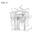
- a push contact type connector 402 may be mounted on the printed circuit board 20 as in a photo detection device 400 according to a third variant shown in Fig. 11 .
- the printed circuit boards 10 and 20 are connected by the connection pin 32, but the present invention is not limited thereto, and the printed circuit boards 10 and 20 may be connected by a flexible printed circuit board 501 as in a photo detection device 500 according to a fourth variant shown in Fig. 12 .
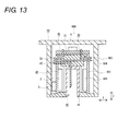
- a printed circuit board 601 arranged to face the printed circuit board 20 with the connector unit 40 interposed therebetween, a microcomputer 602 for automatic air conditioner control mounted on the printed circuit board 601, a connection pin 603 for electrically connecting the printed circuit board 601 and the printed circuit board 10, and a connection pin 604 for electrically connecting the printed circuit board 601 and the printed circuit board 20 may be further arranged as in a photo detection device 600 according to a fifth variant shown in Fig. 13 .
- the printed circuit board 601 serves as a "third board” according to embodiments of the present invention
- the microcomputer 602 serves as a "second signal processing unit” according to embodiments of the present invention.
- the lens 50b for the insolation sensor 4 and the lens 50c for the illuminance sensor 1 are formed on the upper surface 50a of the housing 50, but the present invention is not limited thereto, and the lens 50b for the insolation sensor 4 and the lens 50c for the illuminance sensor 1 may be removably attached to the upper surface 50a of the housing 50.
- the headlight switch 153 outputs the light ON command or the light OFF command of the headlight 151 to the vehicle control unit 156, but the present invention is not limited thereto, and the headlight switch 153 may directly output the light ON command or the light OFF command to the headlight 151.
- the taillight switch 154 may directly output the light ON command or the light OFF command to the headlight 151.
Landscapes
- Physics & Mathematics (AREA)
- General Physics & Mathematics (AREA)
- Spectroscopy & Molecular Physics (AREA)
- Life Sciences & Earth Sciences (AREA)
- Sustainable Development (AREA)
- Thermal Sciences (AREA)
- Engineering & Computer Science (AREA)
- Mechanical Engineering (AREA)
- Photometry And Measurement Of Optical Pulse Characteristics (AREA)
- Lighting Device Outwards From Vehicle And Optical Signal (AREA)
Abstract
Description
- The present invention relates to a photo detection device arranged in a vehicle.
- Conventionally, there is known a photo detection device arranged in a vehicle for automatically controlling an air conditioner of the vehicle. The photo detection device includes an insolation sensor for detecting an insolation amount that enters inside the vehicle from outside the vehicle. In a vehicle arranged with the photo detection device, an amount of heat to which a passenger of the vehicle is exposed is determined based on a detection result of the insolation sensor, and the air conditioner is controlled according to the determined amount of heat.
- Conventionally, there is also known a photo detection device arranged in a vehicle for automatically controlling lights of the vehicle (see e.g., Japanese Patent No.
3504407 - The photo detection device described in Japanese Patent No.
3504407 - However, the photo detection device disclosed in Japanese Patent No.
3504407 - The present invention has been devised to provide a photo detection device that can facilitate assembly while realizing miniaturization.
- In accordance with one aspect of the present invention, a photo detection device of the present invention relates to a photo detection device arranged in a vehicle, the device including: a first photo detection element for detecting light; a first signal processing unit for performing a predetermined process based on a detection result of the first photo detection element; a first board on which the first photo detection element is mounted; a second board on which the first signal processing unit is mounted; a holding member for holding the first board and the second board; and a housing for accommodating the holding member, wherein the holding member holds the first board and the second board so that the second board is arranged in a plane different from a plane in which the first board is arranged.
- Since the first board on which the first photo detection element is mounted and the second board on which the first signal processing unit is mounted are separately arranged, and the second board is arranged in a plane different from a plane in which the first board is arranged, the first board and the second board are stereoscopically arranged, the photo detection device can be miniaturized as compared to the case in which the first photo detection element and the first signal processing unit are mounted on one board. Furthermore, by arranging the holding member for holding the first board and the second board, the holding member can be accommodated in the housing after attaching the first board and the second board to the holding member. Therefore, the accommodation to the housing is facilitated. As a result, the assembly can be facilitated while realizing miniaturization.
- In the above photo detection device, the holding member may hold the first board and the second board so that the plane in which the first board is arranged and the plane in which the second board is arranged are orthogonal.
- In the above photo detection device, the holding member may be formed with an engagement part that engages with the housing.
- The above photo detection device may further include a connector unit held by the holding member, wherein the holding member holds the first board at an upper side of the connector unit and holds the second board at a side of the connector unit.
- The above photo detection device may further include a communication circuit, mounted on the second board, for outputting a processing signal from the first signal processing unit with a digital signal.
- The above photo detection device may further compriseinclude a second photo detection element for detecting light, wherein the second photo detection element may be mounted on the first board.
- In this case, the photo detection device may further include a second signal processing unit for performing a predetermined process based on a detection result of the second photo detection element.
- In the photo detection device including the second signal processing unit, the second signal processing unit may be mounted on the second board.
- The photo detection device including the second signal processing unit, may further include a third board on which the second signal processing unit is mounted, wherein the holding member holds the third board so that the third board is arranged in a plane different from a plane in which the first board is arranged.
- According to embodiments of the present invention, the photo detection device that can facilitate the assembly while realizing miniaturization can be provided.
-
Fig. 1 is a block diagram showing a configuration of a photo detection device and a vehicle according to one embodiment of the present invention; -
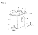
Fig. 2 is a perspective view showing a structure of the photo detection device ofFig. 1 ; -
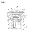
Fig. 3 is a cross-sectional view taken along line 1000-1000 of a state in which the photo detection device ofFig. 2 is attached to a dashboard; -
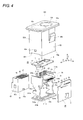
Fig. 4 is an exploded perspective view showing the structure of the photo detection device ofFig. 2 ; -
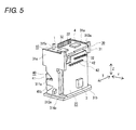
Fig. 5 is a perspective view showing a state in which a housing of the photo detection device ofFig. 2 is removed; -
Fig. 6 is an exploded perspective view showing a holding member and a connector unit of the photo detection device ofFig. 2 ; -
Fig. 7 is a perspective view for describing a method of assembling a photo detection device according to one embodiment of the present invention; -
Fig. 8 is a perspective view for describing a method of assembling a photo detection device according to one embodiment of the present invention; -
Fig. 9 is a cross-sectional view showing a photo detection device according to a first variant of the present embodiment; -
Fig. 10 is a cross-sectional view showing a photo detection device according to a second variant of the present embodiment; -
Fig. 11 is a cross-sectional view showing a photo detection device according to a third variant of the present embodiment; -
Fig. 12 is a cross-sectional view showing a photo detection device according to a fourth variant of the present embodiment; and -
Fig. 13 is a cross-sectional view showing a photo detection device according to a fifth variant of the present embodiment. - Hereinafter, embodiments of the present invention will be described with reference to the drawings.
- First, a configuration of a
photo detection device 100 and avehicle 150 according to one embodiment of the present invention will be described with reference toFig. 1 . - As shown in
Fig. 1 , thevehicle 150 includes aheadlight 151, ataillight 152, aheadlight switch 153, ataillight switch 154, aphoto detection device 100, anair conditioner 155, and avehicle control unit 156. - The
vehicle 150 is an automatic four wheel vehicle or the like. Theheadlight 151 is arranged at the front end of thevehicle 150. Theheadlight 151 is arranged to illuminate so that a driver (passenger) can visually see the front side of thevehicle 150. Thetaillight 152 is arranged at the back end of thevehicle 150. Thetaillight 152 is arranged to notify the existence of the own vehicle to the following vehicles. - The
headlight switch 153 outputs a light-ON command or a light-OFF command of theheadlight 151 to thevehicle control unit 156 by being operated by the driver. In other words, theheadlight switch 153 is a manual switch for controlling the light-ON/OFF state of theheadlight 151. - The
taillight switch 154 outputs a light-ON command or a light-OFF command of thetaillight 152 to thevehicle control unit 156 by being operated by the driver. In other words, thetaillight switch 154 is a manual switch for controlling the light-ON/OFF state of thetaillight 152. - The
photo detection device 100 includes anilluminance sensor 1, amicrocomputer 2, acommunication circuit 3, and aninsolation sensor 4. The structure of thephoto detection device 100 will be described in detail later. Theilluminance sensor 1 serves as a "first photo detection element" according to embodiments of the present invention and themicrocomputer 2 serves as a "first signal processing unit" according to embodiments of the present invention. Theinsolation sensor 4 serves as a "second photo detection element" according to embodiments of the present invention. - The
illuminance sensor 1 detects the illuminance of the periphery of thevehicle 150. Themicrocomputer 2 is configured by a CPU, a ROM, a RAM, and the like, and outputs a control signal (light-ON command or light-OFF command) for controlling theheadlight 151 and thetaillight 152 to thevehicle control unit 156 based on a detection result of theilluminance sensor 1. - Specifically, the
microcomputer 2 determines that the periphery of thevehicle 150 is dark and outputs the light-ON command of theheadlight 151 and thetaillight 152 when the illuminance detected by theilluminance sensor 1 is smaller than a predetermined threshold value. Themicrocomputer 2 determines that the periphery of thevehicle 150 is bright and outputs the light-OFF command of theheadlight 151 and thetaillight 152 when the illuminance detected by theilluminance sensor 1 is greater than a predetermined threshold value. In other words, theilluminance sensor 1 and themicrocomputer 2 configure an automatic light control device for automatically controlling the light-ON/OFF state of theheadlight 151 and thetaillight 152. - The
communication circuit 3 is a CAN (Controller Area Network) transceiver, for example, and is arranged to digitally communicate with thevehicle control unit 156, and the like. For example, thecommunication circuit 3 transmits the light-ON command and the light-OFF command (processing signal from the microcomputer 2) to thevehicle control unit 156 in digital signals. - The
insolation sensor 4 detects an amount of insolation entering inside the vehicle from outside the vehicle. Theair conditioner 155 is arranged to adjust the temperature in the compartment of thevehicle 150. Theair conditioner 155 is configured to determine an amount of heat the passenger of thevehicle 150 receives based on the detection result of theinsolation sensor 4, and automatically adjust the temperature in the compartment of thevehicle 150. - The
vehicle control unit 156 includes acommunication circuit 156a and amicrocomputer 156b. Thecommunication circuit 156a is a CAN transceiver, for example, and is arranged to digitally communicate with thephoto detection device 100, and the like. For example, thecommunication circuit 156a receives the light-ON command and the light-OFF command transmitted from thephoto detection device 100. - The
microcomputer 156b is configured by a CPU, a ROM, a RAM, and the like, and controls the operation of thevehicle 150. For example, themicrocomputer 156b turns ON theheadlight 151 when the light ON command is inputted from theheadlight switch 153, and turns OFF theheadlight 151 when the light OFF command is inputted from theheadlight switch 153. Themicrocomputer 156b also turns ON thetaillight 152 when the light ON command is inputted from thetaillight switch 154, and turns OFF thetaillight 152 when the light OFF command is inputted from thetaillight switch 154. - The
microcomputer 156b also turns ON theheadlight 151 and thetaillight 152 when thecommunication circuit 156a receives the light ON command transmitted from thephoto detection device 100, and turns OFF theheadlight 151 and thetaillight 152 when thecommunication circuit 156a receives the light OFF command transmitted from thephoto detection device 100. - The structure of the
photo detection device 100 according to one embodiment of the present invention will now be described with reference toFig. 2 to Fig. 6 . - The photo detection device 100 (see
Fig. 2 ) according to the present embodiment is inserted to anattachment hole 157a formed in thedashboard 157 of thevehicle 150, as shown inFig. 3 . As shown inFig. 4 , thephoto detection device 100 includes printedcircuit boards member 30, aconnector unit 40, and ahousing 50. The printedcircuit boards - The
illuminance sensor 1 and theinsolation sensor 4 are mounted on the printedcircuit board 10. The printedcircuit board 10 is also formed with aconnection hole 11 for electrically connecting with the printedcircuit board 20, and apositioning hole 12 for positioning. A plurality of connection holes 11 (eight in the present embodiment) are formed at a predetermined interval in the X direction. - The microcomputer 2 (see
Fig. 3 ) and thecommunication circuit 3 are mounted on the printedcircuit board 20. The printedcircuit board 20 is also formed with aconnection hole 21 for electrically connecting with the printedcircuit board 10, and aconnection hole 22 to which aconnection terminal 42 of theconnector unit 40 is electrically connected. A plurality of connection holes 21 (eight in the present embodiment) are formed at a predetermined interval in the X direction. A plurality of connection holes 22 (seven in the present embodiment) are formed at a predetermined interval in the X direction on the lower side of the plurality of connection holes 21. - As shown in
Fig. 5 , the holdingmember 30 holds the printedcircuit board 10 so as to be orthogonal to the Z direction, and holds the printedcircuit board 20 so as to be orthogonal to the Y direction. A plane in which the printedcircuit board 10 is arranged and a plane in which the printedcircuit board 20 is arranged are thus orthogonal. The holdingmember 30 also holds theconnector unit 40. - As shown in
Fig. 4 , the holdingmember 30 includes a holding membermain body 31 formed by resin, and aconnection pin 32 for electrically connecting the printedcircuit boards main body 31 includes a pair ofside plate portions 31 a andcoupling portions side plate portions 31 a. - The pair of
side plate portions 31 a is formed with anengagement part 311 a for holding theconnector unit 40, and is also formed with anengagement part 312a for attaching the holdingmember 30 to thehousing 50. Theengagement part 311 a is formed to project out to the inner side in the X direction. Theengagement part 312a is formed to project out to the outer side in the X direction. - A
step difference 313a for arranging the printedcircuit board 10 between the pair ofside plate portions 31 a is formed at the upper end of the pair ofside plate portions 31 a. Aprojection 314a that projects out to the side is formed at the lower end of the pair ofside plate portions 31 a. - A
coupling portion 31 b is formed at the lower end of the pair ofside plate portions 31 a and is formed to project out to one side in the Y direction. Thecoupling portion 31 b includes acontact portion 311 b that comes into contact with the printedcircuit board 20, and apositioning part 312b for positioning theconnector unit 40. - A
coupling portion 31 c includes agroove 311 c, in which aconnection pin 32 is arranged, and aninsertion hole 312c to which theconnection pin 32 is inserted. Pluralities ofgrooves 311 c andinsertion holes 312c (eight each in the present embodiment) are formed at a predetermined interval in the X direction. Thegroove 311 c (seeFig. 6 ) is formed to extend in the Z direction and theinsertion hole 312c (seeFig. 4 ) is formed to extend in the Y direction. - The
coupling portion 31 c includes aninsertion hole 313c, to which theconnection terminal 42 of theconnector unit 40 is inserted, acontact portion 314c that comes into contact with the printedcircuit board 20, and apositioning pin 315c for positioning the printedcircuit board 10. A plurality ofinsertion holes 313c (seven in the present embodiment) are formed at a predetermined interval in the X direction and are formed to extend in the Y direction. Thepositioning pin 315c is formed to extend in the Z direction, and is inserted to thepositioning hole 12 of the printedcircuit board 10. - A plurality of connection pins 32 (eight in the present embodiment) are formed at a predetermined interval in the X direction. As shown in
Fig. 3 , theconnection pin 32 is formed to an L shape in side view, and is attached to the holding membermain body 31. Theconnection pin 32 has one end soldered while being inserted to theconnection hole 11 of the printedcircuit board 10, and the other end soldered while being inserted to theconnection hole 21 of the printedcircuit board 20. - The
connector unit 40 is arranged to communicate with the vehicle control unit 156 (seeFig. 1 ) and the like, and outputs the detection result of theinsolation sensor 4 to the air conditioner 155 (seeFig. 1 ). Theconnector unit 40 is arranged on the lower side of the printedcircuit board 10 and on the side of the printedcircuit board 20. - The
connector unit 40 includes abox member 41 formed by resin, and aconnection terminal 42 attached to thebox member 41. Thebox member 41 has anopening 41 a formed at the lower end, and is configured so that an external connector (not shown) can be attached. As shown inFig. 4 , thebox member 41 is formed with anengagement part 41 b that engages theengagement part 311 a of the holdingmember 30, and is also formed with aprojection 41 c arranged on thepositioning part 312b of the holdingmember 30. - A plurality of connection terminals 42 (seven in the present embodiment) are formed at a predetermined interval in the X direction. As shown in
Fig. 3 , theconnection terminal 42 is formed to an L shape in side view and has one end soldered while being inserted to the connection hole 22 (seeFig. 4 ) of the printedcircuit board 20. - The
housing 50 is made of resin and is formed to a box shape with the lower end opened. The holdingmember 30 for holding the printedcircuit boards connector unit 40 is attached to thehousing 50. The printedcircuit boards member 30, and theconnector unit 40 are thus accommodated inside thehousing 50. - A
lens 50b for theinsolation sensor 4 and alens 50c for theilluminance sensor 1 are formed on theupper surface 50a of thehousing 50. Thelenses lens 50b is formed on the upper side of theinsolation sensor 4 so as to correspond with theinsolation sensor 4. Thelens 50c is formed on the upper side of theilluminance sensor 1 so as to correspond with theiluminance sensor 1. - In a
surface 50d orthogonal to the X direction of thehousing 50, anengagement hole 50e that engages with theengagement part 312a of the holdingmember 30 is formed in the vicinity of the lower end of thesurface 50d and acutout 50f in which theprojection 314a of the holdingmember 30 is arranged is formed at the lower end of thesurface 50d. Further, in asurface 50g orthogonal to the Y direction of thehousing 50, anail portion 50h for attaching thehousing 50 to theattachment hole 157a (seeFig. 3 ) of thedashboard 157 is formed. - The method of assembling the
photo detection device 100 according to one embodiment of the present invention will now be described with reference toFig. 2 to Fig. 8 . - The
connector unit 40 is first moved in the Y direction from the state shown inFig. 4 to insert theconnection terminal 42 of theconnector unit 40 to theinsertion hole 313c of the holdingmember 30. Thereafter, theconnector unit 40 is further moved in the Y direction so that theprojection 41c of theconnector unit 40 is arranged in thepositioning part 312b of the holdingmember 30 and theengagement part 41 b of theconnector unit 40 is engaged with theengagement part 311 a of the holdingmember 30, as shown inFig. 7 . Theconnector unit 40 is thereby attached to the holdingmember 30. - The printed
circuit board 20 is then moved in the Y direction from the state shown inFig. 7 so that theconnection pin 32 of the holdingmember 30 is inserted to theconnection hole 21 of the printedcircuit board 20 and theconnection terminal 42 of theconnector unit 40 is inserted to theconnection hole 22 of the printedcircuit board 20. The printedcircuit board 20 is moved in the Y direction until the printedcircuit board 20 comes into contact with thecontact portions member 30. Thereafter, theconnection pin 32 is soldered to the printedcircuit board 20 and theconnection terminal 42 is soldered to the printedcircuit board 20 with the printedcircuit board 20 in contact with thecontact portions member 30. The printedcircuit board 20 is thereby attached to the holdingmember 30 so as to be orthogonal to the Y direction, as shown inFig. 8 . - The printed
circuit board 10 is then moved in the Z direction from the state shown inFig. 8 so that thepositioning pin 315c of the holdingmember 30 is inserted to thepositioning hole 12 of the printedcircuit board 10 and theconnection pin 32 of the holdingmember 30 is inserted to theconnection hole 11 of the printedcircuit board 10. The printedcircuit board 10 is moved in the Z direction until the printedcircuit board 10 is arranged on thestep difference 313a of the holdingmember 30. Subsequently, theconnection pin 32 is soldered to the printedcircuit board 10 with the printedcircuit board 10 arranged on thestep difference 313a of the holdingmember 30. The printedcircuit board 10 is thereby attached to the holdingmember 30 so as to be orthogonal to the Z direction, as shown inFig. 5 . - The holding
member 30 holding the printedcircuit boards connector unit 40 is then inserted from the opening formed at the lower end of the housing 50 (seeFig. 4 ). When theengagement part 312a of the holdingmember 30 engages with theengagement hole 50e of thehousing 50, the holdingmember 30 holding the printedcircuit boards connector unit 40 is attached to thehousing 50, as shown inFig. 2 . In this case, theprojection 314a of the holdingmember 30 is arranged in thecutout 50f of thehousing 50. - In the present embodiment, as described above, the printed
circuit board 10 mounted with theilluminance sensor 1 and the printedcircuit board 20 mounted with themicrocomputer 2 are separately arranged, where the printedcircuit board 20 is arranged in a plane different from a plane in which the printedcircuit board 10 is arranged. With such a configuration, the printedcircuit boards photo detection device 100 can be miniaturized as compared to the case of mounting the illuminance sensor and the microcomputer on one printed circuit board. Furthermore, the holdingmember 30 for holding the printedcircuit boards member 30 can be accommodated in thehousing 50 after attaching the printedcircuit boards member 30. The accommodation to thehousing 50 is thereby facilitated. As a result, assembly can be facilitated while realizing miniaturization. - In the present embodiment, the
photo detection device 100 is effectively miniaturized by having the plane in which the printedcircuit board 10 is arranged and the plane in which the printedcircuit board 20 is arranged orthogonal to each other. - In the present embodiment, the
connector unit 40 is arranged on the lower side of the printedcircuit board 10 and at the side of the printedcircuit board 20, so that theconnector unit 40 can be arranged while realizing miniaturization of thephoto detection device 100 by effectively using a rectangular parallelepiped space formed by the printedcircuit boards - In the present embodiment, the
communication circuit 3 for transmitting the light ON command and the light OFF command to thevehicle control unit 156 with the digital signal is arranged, so that the influence of noise can be suppressed compared to the case of outputting the detection result of theilluminance sensor 1 with the analog signal. The reliability of the automatic light control thus can be suppressed from lowering. - In the present embodiment, the
insolation sensor 4 is also mounted on the printedcircuit board 10 on which theilluminance sensor 1 is mounted so that the temperature in the compartment of thevehicle 150 can be automatically adjusted without separately arranging the photo detection device for controlling theair conditioner 155. - In the present embodiment, the
engagement part 312a is formed in the holdingmember 30, and theengagement hole 50e is formed in thehousing 50. Thus, the holdingmember 30 can be easily attached to thehousing 50 by engaging theengagement part 312a of the holdingmember 30 to theengagement hole 50e of thehousing 50 without using an adhesive or the like. - The present invention may adopt various embodiments other than the above. For example, in the above embodiment, an example is shown in which the plane in which the printed
circuit board 10 is arranged and the plane in which the printedcircuit board 20 is arranged are orthogonal, but the present invention is not limited thereto, and the printedcircuit board 20 merely needs to be arranged in the plane different from the plane in which the printedcircuit board 10 is arranged. For example, the printedcircuit board 20 may be arranged parallel to the printedcircuit board 10 at the lower side of theboard 10. In this case, each projection face of theboard circuit board 20 may be arranged to incline with respect to the printedcircuit board 10. - In the above embodiment, an example is shown in which the
illuminance sensor 1 and theinsolation sensor 4 are mounted on the printedcircuit board 10, but the present invention is not limited thereto, and only theilluminance sensor 1 may be mounted on the printedcircuit board 10. Furthermore, only the insolation sensor (first photo detection element) 4 may be mounted on the printedcircuit board 10. In this case, a microcomputer (first signal processing unit) for automatic air conditioner control is mounted on the printedcircuit board 20 in place of themicrocomputer 2 configuring the automatic light control device. - In the above embodiment, the
microcomputer 201 for automatic air conditioner control may be mounted on the printedcircuit board 20 in addition to themicrocomputer 2 as in thephoto detection device 200 according to a first variant shown inFig. 9 . Themicrocomputer 201 serves as a "second signal processing unit" according to embodiments of the present invention. According to this configuration, since the control signal for automatic air conditioner control can be outputted with the digital signal, the influence of noise can be suppressed from being received compared to the case of outputting the detection result of theinsolation sensor 4 with the analog signal. - In the above embodiment, an example is shown in which the
connection pin 32 is soldered to the printedcircuit board 10 and theconnection pin 32 and theconnection terminal 42 are soldered to the printedcircuit board 20, but the present invention is not limited thereto, and theconnector 301 to which theconnection pin 32 is inserted may be mounted on the printedcircuit board 10 and the connector 302 to which theconnection pin 32 and theconnection terminal 42 are inserted may be mounted on the printedcircuit board 20 as in thephoto detection device 300 according to a second variant shown inFig. 10 . A push contact type connector 401 may be mounted on the printedcircuit board 10, and a push contact type connector 402 may be mounted on the printedcircuit board 20 as in aphoto detection device 400 according to a third variant shown inFig. 11 . - In the above embodiment, an example is shown in which the printed
circuit boards connection pin 32, but the present invention is not limited thereto, and the printedcircuit boards circuit board 501 as in aphoto detection device 500 according to a fourth variant shown inFig. 12 . - In the above embodiment, a printed
circuit board 601 arranged to face the printedcircuit board 20 with theconnector unit 40 interposed therebetween, amicrocomputer 602 for automatic air conditioner control mounted on the printedcircuit board 601, aconnection pin 603 for electrically connecting the printedcircuit board 601 and the printedcircuit board 10, and aconnection pin 604 for electrically connecting the printedcircuit board 601 and the printedcircuit board 20 may be further arranged as in aphoto detection device 600 according to a fifth variant shown inFig. 13 . The printedcircuit board 601 serves as a "third board" according to embodiments of the present invention, and themicrocomputer 602 serves as a "second signal processing unit" according to embodiments of the present invention. - In the above embodiment, an example is shown in which the
lens 50b for theinsolation sensor 4 and thelens 50c for theilluminance sensor 1 are formed on theupper surface 50a of thehousing 50, but the present invention is not limited thereto, and thelens 50b for theinsolation sensor 4 and thelens 50c for theilluminance sensor 1 may be removably attached to theupper surface 50a of thehousing 50. - In the above embodiment, an example is shown in which the
headlight switch 153 outputs the light ON command or the light OFF command of theheadlight 151 to thevehicle control unit 156, but the present invention is not limited thereto, and theheadlight switch 153 may directly output the light ON command or the light OFF command to theheadlight 151. The same also applies for thetaillight switch 154.
Claims (9)
- A photo detection device (100, 200, 300, 400, 500, 600) arranged in a vehicle, the photo detection device comprising:a first photo detection element (1) for detecting light;a first signal processing unit (2) for performing a predetermined process based on a detection result of the first photo detection element (1);a first board (10) on which the first photo detection element (1) is mounted;a second board (20) on which the first signal processing unit (2) is mounted;a holding member (30) for holding the first board (10) and the second board (20); anda housing (50) for accommodating the holding member (30), whereinthe holding member (30) holds the first board (10) and the second board (20) so that the second board (20) is arranged in a plane different from a plane in which the first board (10) is arranged.
- The photo detection device (100, 200, 300, 400, 500, 600) according to claim 1, wherein
the holding member (30) holds the first board (10) and the second board (20) so that the plane in which the first board (10) is arranged and the plane in which the second board (20) is arranged are orthogonal. - The photo detection device (100, 200, 300, 400, 500, 600) according to claim 1 or 2, wherein
the holding member (30) is formed with an engagement part (312a) that engages with the housing (50). - The photo detection device (100, 200, 300, 400, 500, 600) according to any of claims 1 to 3, further comprising
a connector unit (40) held by the holding member (30), wherein
the holding member (30) holds the first board (10) at an upper side of the connector unit (40) and holds the second board (20) at a side of the connector unit (40). - The photo detection device (100, 200, 300, 400, 500, 600) according to any of claims 1 to 4, further comprising
a communication circuit (3), mounted on the second board (20), for outputting a processing signal from the first signal processing unit (2) with a digital signal. - The photo detection device (100, 200, 300, 400, 500, 600) according to any of claims 1 to 5, further comprising
a second photo detection element (4) for detecting light, wherein
the second photo detection element (4) is mounted on the first board (10). - The photo detection device (100, 200, 300, 400, 500, 600) according to claim 6, further comprising
a second signal processing unit (201, 602) for performing a predetermined process based on a detection result of the second photo detection element (4). - The photo detection device (100, 200, 300, 400, 500, 600) according to claim 7, wherein
the second signal processing unit (201) is mounted on the second board (20). - The photo detection device (100, 200, 300, 400, 500, 600) according to claim 7, further comprising
a third board (601) on which the second signal processing unit (602) is mounted, wherein
the holding member (30) holds the third board (601) so that the third board (601) is arranged in a plane different from a plane in which the first board (10) is arranged.
Applications Claiming Priority (1)
| Application Number | Priority Date | Filing Date | Title |
|---|---|---|---|
| JP2010097714A JP5473745B2 (en) | 2010-04-21 | 2010-04-21 | Photodetector |
Publications (2)
| Publication Number | Publication Date |
|---|---|
| EP2381229A2 true EP2381229A2 (en) | 2011-10-26 |
| EP2381229A3 EP2381229A3 (en) | 2013-06-19 |
Family
ID=44358274
Family Applications (1)
| Application Number | Title | Priority Date | Filing Date |
|---|---|---|---|
| EP11163202.2A Withdrawn EP2381229A3 (en) | 2010-04-21 | 2011-04-20 | Photo detection device |
Country Status (4)
| Country | Link |
|---|---|
| US (1) | US8963062B2 (en) |
| EP (1) | EP2381229A3 (en) |
| JP (1) | JP5473745B2 (en) |
| CN (1) | CN102252751B (en) |
Cited By (1)
| Publication number | Priority date | Publication date | Assignee | Title |
|---|---|---|---|---|
| CN104108341A (en) * | 2014-07-17 | 2014-10-22 | 湖北开特汽车电子电器系统股份有限公司 | Multifunctional optical sensor device with alarm lamp |
Families Citing this family (7)
| Publication number | Priority date | Publication date | Assignee | Title |
|---|---|---|---|---|
| JP5948978B2 (en) * | 2012-03-06 | 2016-07-06 | 株式会社デンソー | Sensor connector |
| JP5811920B2 (en) * | 2012-03-27 | 2015-11-11 | 株式会社デンソー | LIGHT SENSOR FOR VEHICLE AND VEHICLE STATUS NOTIFICATION DEVICE |
| JP6120799B2 (en) | 2013-05-21 | 2017-04-26 | オムロンオートモーティブエレクトロニクス株式会社 | Photodetector |
| US9891100B2 (en) * | 2013-10-10 | 2018-02-13 | Apple, Inc. | Electronic device having light sensor package with diffuser for reduced light sensor directionality |
| JP2022148746A (en) | 2021-03-24 | 2022-10-06 | 本田技研工業株式会社 | Optical detection device and vehicle |
| US12504322B2 (en) * | 2023-11-29 | 2025-12-23 | United States of America, Dept. of the Navy | Removable photo diode case |
| WO2026053726A1 (en) * | 2024-09-04 | 2026-03-12 | コニカミノルタ株式会社 | Photometric/colorimetric device |
Citations (1)
| Publication number | Priority date | Publication date | Assignee | Title |
|---|---|---|---|---|
| JP3504407B2 (en) | 1995-11-01 | 2004-03-08 | ナイルス株式会社 | Optical sensor sensitivity adjustment device |
Family Cites Families (21)
| Publication number | Priority date | Publication date | Assignee | Title |
|---|---|---|---|---|
| JPH0448504Y2 (en) | 1986-02-28 | 1992-11-16 | ||
| DE4041770C1 (en) * | 1990-12-24 | 1992-07-16 | Hella Kg Hueck & Co, 4780 Lippstadt, De | |
| DE69323618T3 (en) * | 1992-11-06 | 2005-02-03 | Denso Corp., Kariya | PYRHELIOMETRIC SENSOR |
| JP3579455B2 (en) * | 1994-05-06 | 2004-10-20 | ペンタックス株式会社 | Image input device |
| JP3518030B2 (en) * | 1995-03-17 | 2004-04-12 | 株式会社デンソー | Optical sensor device |
| JP3783451B2 (en) * | 1999-03-12 | 2006-06-07 | 株式会社デンソー | Optical sensor |
| US6521882B1 (en) | 1998-03-27 | 2003-02-18 | Denso Corporation | Optical sensor with directivity controlled |
| JP3800880B2 (en) * | 1999-08-26 | 2006-07-26 | 松下電工株式会社 | Receiver unit |
| CA2349093A1 (en) * | 2001-05-29 | 2002-11-29 | Silonex Inc. | Sunload sensor for automotive vehicules |
| JP2003337178A (en) * | 2002-05-21 | 2003-11-28 | Matsushita Electric Works Ltd | Sensor unit |
| US20040217258A1 (en) * | 2003-04-30 | 2004-11-04 | Clugston P. Edward | Solar sensor including reflective element to transform the angular response |
| SE0301857D0 (en) * | 2003-06-24 | 2003-06-24 | Uab Accel Elektronika | An optical radiation intensity sensor |
| JP4134912B2 (en) * | 2004-01-22 | 2008-08-20 | 株式会社デンソー | Photodetector |
| JP2005233728A (en) * | 2004-02-18 | 2005-09-02 | Denso Corp | Optical sensor device |
| JP2005238921A (en) * | 2004-02-25 | 2005-09-08 | Denso Corp | Compound sensor |
| CN2709226Y (en) * | 2004-06-17 | 2005-07-13 | 上海中油企业集团有限公司 | Dust detector used on ventilation device of car |
| DE102005011053A1 (en) * | 2005-03-10 | 2006-09-21 | Preh Gmbh | Sun sensor in MID technology |
| DE102008033204A1 (en) * | 2008-07-15 | 2010-02-04 | Trw Automotive Electronics & Components Gmbh | Optical sensor |
| GB2461917A (en) * | 2008-07-18 | 2010-01-20 | Gm Global Tech Operations Inc | Integrated sensor assembly for vehicle containing plurality of sensor types and theft deterrent LED |
| CN201281628Y (en) * | 2008-10-31 | 2009-07-29 | 湖北开特汽车电子电器系统有限公司 | Sunshine/circumstance light integrated sensor for automobile air conditioner and light control |
| CN101446541B (en) * | 2008-12-30 | 2011-01-05 | 吉林大学 | A smoke detection system for automobile engine compartment |
-
2010
- 2010-04-21 JP JP2010097714A patent/JP5473745B2/en not_active Expired - Fee Related
-
2011
- 2011-04-20 EP EP11163202.2A patent/EP2381229A3/en not_active Withdrawn
- 2011-04-20 CN CN201110099483.1A patent/CN102252751B/en not_active Expired - Fee Related
- 2011-04-21 US US13/091,734 patent/US8963062B2/en active Active
Patent Citations (1)
| Publication number | Priority date | Publication date | Assignee | Title |
|---|---|---|---|---|
| JP3504407B2 (en) | 1995-11-01 | 2004-03-08 | ナイルス株式会社 | Optical sensor sensitivity adjustment device |
Cited By (1)
| Publication number | Priority date | Publication date | Assignee | Title |
|---|---|---|---|---|
| CN104108341A (en) * | 2014-07-17 | 2014-10-22 | 湖北开特汽车电子电器系统股份有限公司 | Multifunctional optical sensor device with alarm lamp |
Also Published As
| Publication number | Publication date |
|---|---|
| CN102252751A (en) | 2011-11-23 |
| US8963062B2 (en) | 2015-02-24 |
| US20110260034A1 (en) | 2011-10-27 |
| JP2011226946A (en) | 2011-11-10 |
| EP2381229A3 (en) | 2013-06-19 |
| CN102252751B (en) | 2014-07-09 |
| JP5473745B2 (en) | 2014-04-16 |
Similar Documents
| Publication | Publication Date | Title |
|---|---|---|
| EP2381229A2 (en) | Photo detection device | |
| JP2010083210A (en) | Light source unit for vehicle interior | |
| CN108808295B (en) | Vehicle-mounted camera | |
| KR101601512B1 (en) | Multifunctional integration module for mounting in the rear of vehicle | |
| WO2006117892A1 (en) | Electric device | |
| JP4601485B2 (en) | Electrical equipment | |
| US20170018377A1 (en) | Switch apparatus having wireless function | |
| KR20190027078A (en) | Camera module and vehicle | |
| RU2004107744A (en) | CAR ON-BOARD INFORMATION SYSTEM | |
| US12324099B2 (en) | Vehicular overhead console with flexible circuit board | |
| JP2019204577A (en) | connector | |
| CN215322338U (en) | Vehicle-mounted camera and motor vehicle | |
| EP2863623A1 (en) | Vehicle camera with an improved connecting device and motor vehicle | |
| JP2010049815A (en) | On-vehicle electric component control unit and control component | |
| JP2005178474A (en) | Mounting structure of oil-filled equipment and control unit | |
| KR101461176B1 (en) | External terminal connecting apparatus | |
| US9457722B2 (en) | Rear view mirror assembly with electrical sub assembly | |
| US20230068758A1 (en) | Camera module for a vehicle | |
| CN109155456B (en) | Communication device for diagnostic system of motor vehicle | |
| KR100451925B1 (en) | Integrated Circuit Module | |
| KR102499801B1 (en) | Variable connector and electronic control device including the same | |
| US9974194B2 (en) | Electronic circuit board unit, electronic module and rear view device for a vehicle | |
| US11768103B2 (en) | Photodetector with improved appearance design and vehicle including photodetector of the same comprising a plurality of electronic components mounted on a light receiving surface side of a printed circuit board | |
| US20250172858A1 (en) | Monitoring camera and associated mounting method | |
| CN115133325A (en) | Photodetector |
Legal Events
| Date | Code | Title | Description |
|---|---|---|---|
| AK | Designated contracting states |
Kind code of ref document: A2 Designated state(s): AL AT BE BG CH CY CZ DE DK EE ES FI FR GB GR HR HU IE IS IT LI LT LU LV MC MK MT NL NO PL PT RO RS SE SI SK SM TR |
|
| AX | Request for extension of the european patent |
Extension state: BA ME |
|
| PUAI | Public reference made under article 153(3) epc to a published international application that has entered the european phase |
Free format text: ORIGINAL CODE: 0009012 |
|
| PUAL | Search report despatched |
Free format text: ORIGINAL CODE: 0009013 |
|
| AK | Designated contracting states |
Kind code of ref document: A3 Designated state(s): AL AT BE BG CH CY CZ DE DK EE ES FI FR GB GR HR HU IE IS IT LI LT LU LV MC MK MT NL NO PL PT RO RS SE SI SK SM TR |
|
| AX | Request for extension of the european patent |
Extension state: BA ME |
|
| RIC1 | Information provided on ipc code assigned before grant |
Ipc: G01J 1/42 20060101AFI20130514BHEP |
|
| 17P | Request for examination filed |
Effective date: 20131217 |
|
| RBV | Designated contracting states (corrected) |
Designated state(s): AL AT BE BG CH CY CZ DE DK EE ES FI FR GB GR HR HU IE IS IT LI LT LU LV MC MK MT NL NO PL PT RO RS SE SI SK SM TR |
|
| STAA | Information on the status of an ep patent application or granted ep patent |
Free format text: STATUS: EXAMINATION IS IN PROGRESS |
|
| 17Q | First examination report despatched |
Effective date: 20180918 |
|
| STAA | Information on the status of an ep patent application or granted ep patent |
Free format text: STATUS: THE APPLICATION IS DEEMED TO BE WITHDRAWN |
|
| 18D | Application deemed to be withdrawn |
Effective date: 20200715 |