EP2378649A2 - Switching scheme for step up-step down converters using fixed frequency current-mode control - Google Patents
Switching scheme for step up-step down converters using fixed frequency current-mode control Download PDFInfo
- Publication number
- EP2378649A2 EP2378649A2 EP20110003282 EP11003282A EP2378649A2 EP 2378649 A2 EP2378649 A2 EP 2378649A2 EP 20110003282 EP20110003282 EP 20110003282 EP 11003282 A EP11003282 A EP 11003282A EP 2378649 A2 EP2378649 A2 EP 2378649A2
- Authority
- EP
- European Patent Office
- Prior art keywords
- buck
- boost mode
- mode
- boost
- transition
- Prior art date
- Legal status (The legal status is an assumption and is not a legal conclusion. Google has not performed a legal analysis and makes no representation as to the accuracy of the status listed.)
- Withdrawn
Links
- 230000007704 transition Effects 0.000 claims abstract description 57
- 230000001939 inductive effect Effects 0.000 claims abstract description 16
- 238000000034 method Methods 0.000 claims abstract description 10
- 230000001276 controlling effect Effects 0.000 claims abstract description 7
- 230000001105 regulatory effect Effects 0.000 claims abstract description 4
- 230000004044 response Effects 0.000 claims abstract description 4
- 230000008878 coupling Effects 0.000 claims description 8
- 238000010168 coupling process Methods 0.000 claims description 8
- 238000005859 coupling reaction Methods 0.000 claims description 8
- 238000010586 diagram Methods 0.000 description 8
- 239000003990 capacitor Substances 0.000 description 5
- 230000004048 modification Effects 0.000 description 4
- 238000012986 modification Methods 0.000 description 4
- 230000001360 synchronised effect Effects 0.000 description 4
- 230000033228 biological regulation Effects 0.000 description 3
Images





Classifications
-
- H—ELECTRICITY
- H02—GENERATION; CONVERSION OR DISTRIBUTION OF ELECTRIC POWER
- H02M—APPARATUS FOR CONVERSION BETWEEN AC AND AC, BETWEEN AC AND DC, OR BETWEEN DC AND DC, AND FOR USE WITH MAINS OR SIMILAR POWER SUPPLY SYSTEMS; CONVERSION OF DC OR AC INPUT POWER INTO SURGE OUTPUT POWER; CONTROL OR REGULATION THEREOF
- H02M3/00—Conversion of DC power input into DC power output
- H02M3/02—Conversion of DC power input into DC power output without intermediate conversion into AC
- H02M3/04—Conversion of DC power input into DC power output without intermediate conversion into AC by static converters
- H02M3/10—Conversion of DC power input into DC power output without intermediate conversion into AC by static converters using discharge tubes with control electrode or semiconductor devices with control electrode
- H02M3/145—Conversion of DC power input into DC power output without intermediate conversion into AC by static converters using discharge tubes with control electrode or semiconductor devices with control electrode using devices of a triode or transistor type requiring continuous application of a control signal
- H02M3/155—Conversion of DC power input into DC power output without intermediate conversion into AC by static converters using discharge tubes with control electrode or semiconductor devices with control electrode using devices of a triode or transistor type requiring continuous application of a control signal using semiconductor devices only
- H02M3/156—Conversion of DC power input into DC power output without intermediate conversion into AC by static converters using discharge tubes with control electrode or semiconductor devices with control electrode using devices of a triode or transistor type requiring continuous application of a control signal using semiconductor devices only with automatic control of output voltage or current, e.g. switching regulators
- H02M3/158—Conversion of DC power input into DC power output without intermediate conversion into AC by static converters using discharge tubes with control electrode or semiconductor devices with control electrode using devices of a triode or transistor type requiring continuous application of a control signal using semiconductor devices only with automatic control of output voltage or current, e.g. switching regulators including plural semiconductor devices as final control devices for a single load
- H02M3/1582—Buck-boost converters
Definitions
- This disclosure relates to power supply systems, and more particularly, to controlling a step up-step down switching regulator using fixed frequency current mode control.
- a step up-step down or a buck-boost switching regulator produces an output voltage VOUT that can be above, below, or at the same level as input voltage VIN.
- FIG. 1 shows a conventional step up-step down switching regulator including an inductor L, switches S 1 and S2 coupled between the input VIN and the inductor L, and switches S3 and S4 coupled between the inductor L and the output VOUT.
- Input capacitor C IN and output capacitor C OUT are respectively coupled to the input VIN and output VOUT.
- a sense resistor R SENSE is provided for sensing current. Current sense inputs SNS+ and SNS- arranged at both sides of the sense resistor R SENSE can supply input signals to a current sense comparator for determining the inductor current I L .
- a voltage divider composed of resistors R1 and R2 provides the output voltage VOUT to a control circuit 10 for regulation.
- the control circuit 10 controls switches S1 to S4 to provide peak current mode regulation in a boost mode when VIN is lower than VOUT, and to provide valley current mode regulation in a buck mode when VIN is higher than VOUT.
- switch S3 in a buck mode (VIN >VOUT), switch S3 (SWITCH 3) is always turned off, and switch S2 (SWITCH 2) is controlled by an error amplifier in the control circuit 10.
- the error amplifier provides an error signal representing a difference between the output voltage VOUT and a reference voltage VREF.
- FIG. 2 shows a clock signal CLOCK used to control switching of the switches S1-S4, and the current I L in the inductor L. In this mode, switch S4 is always turned on, and switch S1 is controlled to provides synchronous rectification.
- FIG. 3 shows the clock signal CLOCK and the inductor current I L .
- the step up-step down regulator When VIN is close to VOUT, the step up-step down regulator operates in a buck-boost mode, in which all switches are turned on and off each cycle. Two cases can exist in the buck-boost mode - the input voltage VIN is slightly less than the output voltage VOUT, or VIN is slightly higher than VOUT.
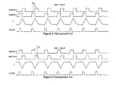
- FIG. 4 illustrates operation of switches S2 and S3 in this mode, and shows the clock signal CLOCK and the inductor current I L .
- FIG. 5 illustrates operation of switches S2 and S3 in this mode, and shows the clock signal CLOCK and the inductor current I L .
- a power supply system for producing a regulated output signal at an output node in response to an input signal at an input node, comprises an inductive device, a plurality of switching circuits for providing connection of the inductive device to the input and output nodes and a ground node, and a switch control circuit for driving the switching devices so as to enable the power supply system to operate in a boost mode to increase the input signal, in a buck mode to decrease the input signal, and in a buck-boost mode when a difference between the input signal and the output signal is within a predetermined range.
- the switch control circuit including buck-boost latch circuitry for latching a transition between the buck mode and the buck-boost mode, or between the boost mode and the buck-boost mode based on a predetermined condition.
- the switching circuits may include:
- the switch control circuit may operate in a valley current control mode to control the switching circuits based on a sensed valley of the inductor current when the power supply system operates in the buck mode, and to operate in a peak current control mode to control the switching circuits based on a sensed peak of the inductor current when the power supply system operates in the boost mode.
- the buck-boost latch circuitry may prevent a transition from the buck or boost mode to the buck-boost mode until on-time of at least one of the switching circuits reaches a preset minimum value.
- the buck-boost latch circuitry may prevent a transition from the buck mode to the buck-boost mode until on-time of the second switching circuit reaches the preset minimum value, and may prevent a transition from the boost mode to the buck-boost mode until on-time of the third switching circuit reaches the preset minimum value.
- the buck-boost latch circuitry may prevent a transition from the buck-boost mode to the buck or boost mode until on-time of at least one of the switching circuits exceeds a preset maximum value.
- the buck-boost latch circuitry may prevent a transition from the buck-boost mode to the buck mode until the on-time of the second switching circuit exceeds the preset maximum value, and may prevent a transition from the buck-boost mode to the boost mode until the on-time of the third switching circuit exceeds the preset maximum value.
- the switch control circuit may include a clock circuit for supplying a first clock signal and a second clock signal provided out of phase with respect to the first clock signal.
- the second clock signal may be provided about 180 degrees out of phase with respect to the first clock signal.
- the first clock signal may be provided to turn on the second switching circuit and the second clock signal may be provided to turn on the third switching circuit.
- the switch control circuit may further include first and second comparators responsive to a sensed inductor current and an error signal representing the output signal to produce signals representing inductor peak current and inductor valley current.
- An exemplary buck-boost latch circuitry may include first and second latching circuits having first inputs respectively responsive to outputs of the first and second comparators, and second inputs respectively supplied with the first and second clock signals produced out of phase with respect to each other.
- First and second duration comparing circuits may be respectively coupled to outputs of the first and second latching circuits for comparing duration values produced at the outputs of the first and second latching circuits with the preset minimum and maximum values, to produce a first control signal at an output of the first duration comparing circuit and to produce a second control signal at an output of the second duration comparing circuit.
- the first control signal may go from a first logic level to a second logic level when the on-time of the second switching circuit becomes less than the preset minimum value to enable a transition from the buck mode to the buck-boost mode.
- the second control signal may go from a first logic level to a second logic level when the on-time of the third switching circuit becomes less than the preset minimum value to enable a transition from the boost mode to the buck-boost mode.
- the first control signal may go from the second logic level to the first logic level when the on-time of the second switching circuit exceeds the preset maximum value to enable a transition from the buck-boost mode to the buck mode.
- the second control signal may go from the second logic level to the first logic level when the on-time of the third switching circuit exceeds the preset maximum value to enable a transition from the buck-boost mode to the boost mode.
- the following steps may be carried out to control a switching regulator having a plurality of switching circuits:
- the transition from the buck mode or the boost mode to the buck-boost mode may be prevented until the on-time of at least one of the switching devices reaches a preset minimum value, and the transition from the buck-boost mode to the buck mode or the boost mode may be prevented until the on-time of at least one of the switching devices exceeds a preset maximum value.
- the switching devices may be controlled by a pair of clock signals produced out of phase with respect to each other.
- the step of preventing a transition may include producing a first control signal that goes from a first logic level to a second logic level when on-time of at least one of the switching devices becomes less than a preset minimum value so as to prevent transition from the buck mode to the buck-boost mode until the on-time reaches the preset minimum value.
- the first control signal may go from the second logic level to the first logic level when the on-time exceeds a preset maximum value so as to prevent transition from the buck-boost mode to the buck mode until the on-time exceeds the preset maximum value.
- the step of preventing a transition may also include producing a second control signal that goes from a first logic level to a second logic level when on-time of at least one of the switching devices becomes less than a preset minimum value so as to prevent transition from the boost mode to the buck-boost mode until the on-time reaches the preset minimum value.
- the second control signal goes from the second logic level to the first logic level when the on-time exceeds a preset maximum value so as to prevent transition from the buck-boost mode to the boost mode until the on-time exceeds the preset maximum value.
- FIG. 1 illustrates an exemplary conventional switching regulator.
- FIGS. 2-5 are timing diagrams illustrating operations of the conventional regulator.
- FIG. 6 schematically shows a control scheme for controlling step up-step down switching regulator in accordance with the present disclosure.
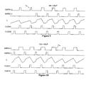
- FIGS. 7 and 8 are timing diagrams that illustrate operations in a buck-boost mode in accordance with the present disclosure.
- FIG. 9 is a timing diagram that illustrates a transition from a buck mode to a buck-boost mode in accordance with the present disclosure.
- FIG. 10 is a timing diagram that illustrates a transition from a buck-boost mode to a buck mode in accordance with the present disclosure..
- FIG. 11 is a timing diagrams that illustrates a transition from a buck-boost mode to a boost mode in accordance with the present disclosure.
- FIG. 12 is a timing diagram that illustrates a transition from a boost mode to a buck-boost mode in accordance with the present disclosure.
- an exemplary step up-step down switching regulator 100 of the present disclosure includes inductor L and switches S1-S4 arranged to provide connection of the inductor L to input node VIN, output node VOUT and a ground node in boost, buck and buck-boost modes.
- the switches S1-S4 are controlled so as to set the regulator into a buck mode of operation.
- the switches S1-S4 are controlled so as to set the regulator into a boost mode of operation.
- the switches S1-S4 are controlled so as to set the regulator into a buck-boost mode of operation.
- Switch control circuitry for controlling the switches S1-S4 includes comparators A 1 and A2, current sense amplifiers A3 and A4, an error amplifier A5, a clock and ramp generator A6, and boost and buck latch circuits A7 and A8.
- the switch control circuitry also includes a first digital comparator 102 composed of one-shot circuits A9, A10, NOR gate circuit A13, AND gate circuit A14 and RS flip flop A17, and a second digital comparator 104 composed of one-shot circuits A11, A 12, NOR gate circuit A115, AND gate circuit A16 and RS flip flop A18.
- the switch control circuitry includes AND gates A19 and A20, and switch drivers A21, A22, A23 and A24.
- the boost and buck latch circuits A7 and A8, together with the digital comparators 102 and 104, and the AND gates A19 and A20, constitute an exemplary buck-boost latch circuitry controlled by a pair of clock signals for latching a transition between the buck mode and the buck-boost mode, or between the boost mode and the buck-boost mode.
- Input capacitor C IN and output capacitor C OUT are respectively coupled to the input VIN and output VOUT.
- a sense resistor R SENSE is provided for sensing current. Current sense inputs SNS+ and SNS- arranged at both sides of the sense resistor R SENSE can supply input signals to the current sense comparators A3 and A4 for determining the inductor current I L .
- a voltage divider composed of resistors RFB1 and RFB2 provides the error amplifier with a signal representing the output voltage VOUT.
- a compensation circuit composed of resistor RC and capacitor CC is connected to the output of the error amplifier A5. Adders A25 and A26 are provided at the inputs of the comparators A1 and A2, respectively.
- the switch control circuitry When the switching regulator 100 operates in the buck mode, the switch control circuitry operates in a valley current control mode, in which the switch control circuit controls the switches S1-S4 based on the sensed valley of the inductor current I L .
- the inverting input of the current sense amplifier A3 is connected to the SNS+ input and the non-inverting input of the amplifier A3 is connected to the SNS- inputs so as to sense the valley of the inductor current I L in the valley current control mode.
- the switch control circuitry When the switching regulator 100 operates in the boost mode, the switch control circuitry operates in a peak current control mode, in which the switch control circuitry controls the switches S1-S4 based on the sensed peak of the inductor current I L .
- the inverting input of the current sense amplifier A4 is connected to the SNS- input and the non-inverting input of the amplifier A4 is connected to the SNS+ inputs, so as to sense the peak of the inductor current I L in the peak current control mode.
- the error amplifier A5 compares a value representing the output voltage VOUT with a reference voltage Vref that may be provided by a reference voltage source, to produce an error signal representing a difference between the output voltage VOUT and the reference voltage Vref.
- the error signal is supplied to the inverting input of the comparator A 1 and the non-inverting input of the comparator A2.
- the non-inverting input of the comparator A1 is fed with an output signal of the adder A25 that adds values of the peak inductor current from the current sense amplifier A4 and a ramp signal from the generator A6.
- the inverting input of the comparator A2 is fed with an output signal of the adder A26 that adds values of the valley inductor current from the current sense amplifier A3 and a ramp signal from the generator A6.
- the comparators A1 and A2 compare their respective inputs to produce signals at their outputs.
- the comparators A1 and A2 may be configured to produce pulse width modulation (PWM) signals at their outputs.
- PWM pulse width modulation
- the comparators A1 and A2 may be configured to have internal hysteresis.
- an external hysteresis network may be arranged at each of the comparators A1 and A2.
- the output of the comparator A1 is supplied to the reset (R) input of the boost latch circuit A7, and the output of the comparator A2 is provided to the R input of the buck latch circuit A8.
- the boost latch circuit A7 is set with a boost clock signal produced by the generator A6, and buck latch circuit A8 is set with a buck clock signal produced by the generator A6 out of phase with respect to the boost clock signal.
- the buck clock signal and boost clock signal may be 180 degrees out of phase.
- the buck clock signal is used by the switch control circuitry to turn on the switch S2
- the boost clock signal is used by the switch control circuitry to turn on the switch S3.
- the outputs of the latch circuits A7 and A8 produce duration values respectively representing the peak and the valley of the inductor current I L .
- the digital comparators 102 and 104 compare these duration values with a predetermined minimum on-time value T MIN and a predetermined maximum on-time value T MAX .
- the minimum on-time value T MIN may correspond to the minimum time interval during which a controlled switch is allowed to be in an on-state.
- the digital comparator 102 includes the one-shot circuit A10 that produces a pulse defining the predetermined T MIN value, and the one-shot circuit A9 that produces a pulse defining the predetermined T MAX value.
- the T MAX value may be selected to be equal to 3T MIN .
- the inputs of the one-shot circuits A9 and A10 are supplied with the signal produced at the output Q of the boost latch circuit A7.
- the output of the one-shot circuit A9 is connected to one input of the NOR gate A13, the other input of which is connected to the inverted output Q/ of the boost latch circuit A7.
- the output of the one-shot circuit A10 is connected to one input of the AND gate A14, the other input of which is connected to the inverted output Q/ of the circuit A7.
- the output signal of the AND gate A14 is used to set the RS flip flop circuit A17, the output signal of the NOR gate A 13 provides reset of the RS flip flop circuit A 17.
- the RS flip flop circuit A 17 produces a control signal ON_BUCK.
- the digital comparator 104 includes the one-shot circuit A12 that produces a pulse defining the predetermined T MIN value, and the one-shot circuit A11 that produces a pulse defining the predetermined T MAX value.
- the T MAX value may be selected to be equal to 3T MIN .
- the inputs of the one-shot circuits A11 and A12 are supplied with the signal produced at the output Q of the buck latch circuit A8.
- the output of the one-shot circuit A11 is connected to one input of the NOR gate A15, the other input of which is connected to the inverted output Q/ of the buck latch circuit A8.
- the output of the one-shot circuit A12 is connected to one input of the AND gate A 16, the other input of which is connected to the inverted output Q/ of the circuit A8.
- the output signal of the AND gate A16 is used to set the RS flip flop circuit A18, the output signal of the NOR gate A15 provides reset of the RS flip flop circuit A18.
- the RS flip flop circuit A17 produces a control signal ON_BOOST.
- the AND gate A19 is supplied with the Q output of the buck latch circuit A8 and the ON_BUCK control signal to produce an output signal that controls switches S1 and S2 via drivers A21 and A22, respectively.
- the AND gate A20 is supplied with the Q output of the boost latch circuit A7 and the ON_BOOST control signal to produce an output signal that controls switches S3 and S4 via drivers A23 and A24, respectively.
- the switches S1-S4 are controlled in the manner similar to operations of a regular switching regulator illustrated in FIG. 2 , i.e. switch S3 is always turned off, switch S4 is always turned on, switch S2 is controlled based on a error signal from the error amplifier A5, and switch S1 is used for providing synchronous rectification.
- the buck clock signal is applied to turn on switch S2.
- the ON_BUCK control signal is at a high level
- the ON_BOOST control signal is at a low level.
- the switches S1-S4 are controlled in the manner similar to operations of a regular switching regulator illustrated in FIG. 3 , i.e. switch S2 is always turned off, switch S 1 is always turned on, switch S3 is controlled based on an error signal from the error amplifier A5, and switch S4 is used for providing synchronous rectification.
- the boost clock signal is applied to turn on switch S3.
- the ON_BOOST control signal is at a high level
- the ON_BUCK control signal is at a low level.
- the step up-step down regulator 100 When VIN is close to VOUT, the step up-step down regulator 100 operates in a buck-boost mode, in which all switches are turned on and off each cycle.
- the regulator 100 may be switched into the buck-boost mode, when a difference between VIN and VOUT is less than a value that may be pre-set, for example, in the range from 500 mV to 1.5 V depending on the clock frequency.
- a value that may be pre-set for example, in the range from 500 mV to 1.5 V depending on the clock frequency.
- Two cases can exist in the buck-boost mode - the input voltage VIN is slightly less than the output voltage VOUT, or VIN is slightly higher than VOUT.
- FIGS. 7-12 show exemplary operations of switches S2 and S3, respectively. It is noted that switch S1 is controlled together with switch S2, and switch S4 is controlled together with switch S3. When switch S2 or S3 is turned on, the respective switch S1 or S4 is turned off, and when the switch S2 or S3 is turned off, the respective switch S1 or S4 is turned on. Also, FIGS. 7-12 illustrate variations of the inductor current I L .
- FIG. 9 illustrates a transition from the buck mode to the buck-boost mode.
- switch S2 is turned on by the buck clock signal CLOCK1 applied via the buck latch circuit A8.
- switch S1 is turned off.
- the duration at the Q output of the buck latch circuit A8 corresponds to the on-time value of the switch S2
- the ON_BOOST signal goes high to enable the boost clock signal CLOCK2 to turn on switch S3 and turn off switch S4, i.e. to allow transition in the buck-boost mode.
- the switch control circuitry prevents a transition from the buck mode to the buck-boost mode until the on-time of the switch S2 reaches a preset minimum value T MIN .
- FIG. 10 illustrates a transition from the buck-boost mode to the buck mode.
- the switch S2 is turned on by the buck clock signal CLOCK1 applied via the buck latch circuit A8, and the switch S3 is turned on by the boost clock signal CLOCK2 applied via the boost latch circuit A7.
- the duration value at the Q output of the buck latch circuit A8 (corresponding to the on-time value of switch S2) exceeds the 3T MIN value (i.e. the T MAX value) defined by the one-shot circuit A11
- the ON_BOOST_signal goes low preventing the switch S3 from being turned on by the boost clock signal CLOCK2.
- the regulator 100 switches to the buck mode.
- the switch control circuitry prevents a transition from the buck-boost mode to the buck mode until the on-time of the switch S2 exceeds a preset maximum value T MAX .
- FIG. 11 illustrates a transition from the buck-boost mode to the boost mode.
- the duration value at the Q output of the boost latch circuit A7 (corresponding to the on-time value of switch S3) exceeds the 3T MIN value (i.e. the T MAX value) defined by the one-shot circuit A9
- the ON_BUCK signal goes low preventing the switch S2 from being turned on by the buck clock signal CLOCK1.
- the switch control circuitry prevents a transition from the buck-boost mode to the boost mode until the on-time of the switch S3 exceeds a preset maximum value T MAX .
- FIG. 12 illustrates a transition from the boost mode to the buck-boost mode.
- switch S3 is turned on by the boost clock signal CLOCK2 applied via the boost latch circuit A7.
- switch S4 is turned off.
- the duration at the Q output of the boost latch circuit A7 corresponds to the on-time value of the switch S3.
- the ON_BUCK signal goes high to enable the buck clock signal CLOCK1 to turn on switch S2 and turn off switch S1, i.e. to allow transition in the buck-boost mode.
- the switch control circuitry prevents a transition from the boost mode to the buck-boost mode until the on-time value of the switch S3 reaches a preset minimum value T MIN .
Landscapes
- Engineering & Computer Science (AREA)
- Power Engineering (AREA)
- Dc-Dc Converters (AREA)
Abstract
Description
- This application claims priority of
US provisional application 61/325,690 filed on April 19, 2010 - This disclosure relates to power supply systems, and more particularly, to controlling a step up-step down switching regulator using fixed frequency current mode control.
- A step up-step down or a buck-boost switching regulator produces an output voltage VOUT that can be above, below, or at the same level as input voltage VIN.
FIG. 1 shows a conventional step up-step down switching regulator including an inductor L,switches S 1 and S2 coupled between the input VIN and the inductor L, and switches S3 and S4 coupled between the inductor L and the output VOUT. Input capacitor CIN and output capacitor COUT are respectively coupled to the input VIN and output VOUT. A sense resistor RSENSE is provided for sensing current. Current sense inputs SNS+ and SNS- arranged at both sides of the sense resistor RSENSE can supply input signals to a current sense comparator for determining the inductor current IL. A voltage divider composed of resistors R1 and R2 provides the output voltage VOUT to a control circuit 10 for regulation. - In particular, the control circuit 10 controls switches S1 to S4 to provide peak current mode regulation in a boost mode when VIN is lower than VOUT, and to provide valley current mode regulation in a buck mode when VIN is higher than VOUT. As illustrated in
FIG. 2 , in a buck mode (VIN >VOUT), switch S3 (SWITCH 3) is always turned off, and switch S2 (SWITCH 2) is controlled by an error amplifier in the control circuit 10. The error amplifier provides an error signal representing a difference between the output voltage VOUT and a reference voltage VREF. Also,FIG. 2 shows a clock signal CLOCK used to control switching of the switches S1-S4, and the current IL in the inductor L. In this mode, switch S4 is always turned on, and switch S1 is controlled to provides synchronous rectification. - As shown in
FIG. 3 , in a boost mode (VIN<VOUT), switch S2 (SWITCH 2) is always turned off and switch S3 (SWITCH 3) is controlled by the error amplifier. In this mode,switch S 1 is always turned on, and switch S4 is controlled to provide synchronous rectification.FIG. 3 also shows the clock signal CLOCK and the inductor current IL. - When VIN is close to VOUT, the step up-step down regulator operates in a buck-boost mode, in which all switches are turned on and off each cycle. Two cases can exist in the buck-boost mode - the input voltage VIN is slightly less than the output voltage VOUT, or VIN is slightly higher than VOUT.
- When the input voltage VIN is slightly less than the output voltage VOUT, switches S1 and S3 turn on at the start of the clock cycle CLOCK. If the error amplifier forces the switches off before some minimum on-time TMIN, then switches S2 and S4 will turn on for a minimum on-time. After switch S2 turns off,
switch S 1 will turn on for the remainder of the clock cycle, and switch S4 will remain in the on-state.FIG. 4 illustrates operation of switches S2 and S3 in this mode, and shows the clock signal CLOCK and the inductor current IL. - When the input voltage VIN is slightly higher than the output voltage VOUT, switches S2 and S4 turn on at the start of the clock cycle CLOCK. If the error amplifier forces the switches off before some minimum on-time TMIN, then
switches switch 1 will remain in the on-state.FIG. 5 illustrates operation of switches S2 and S3 in this mode, and shows the clock signal CLOCK and the inductor current IL. - This conventional switching scheme, works well when the regulator operates purely in a buck mode, or in a boost mode, but not so well in buck-boost mode. During buck-boost mode the switches S1-S4 do not always turn on at a fixed frequency, which may result in increased electromagnetic interference (EMI).
- Hence, there is a need for a control circuit that would control switches of the step up-step down regulator so as to provide switching in a buck-boost mode at a fixed frequency.
- The present disclosure offers novel circuitry and methodology for controlling a step up-step down switching regulator. In accordance with one aspect of the disclosure, a power supply system for producing a regulated output signal at an output node in response to an input signal at an input node, comprises an inductive device, a plurality of switching circuits for providing connection of the inductive device to the input and output nodes and a ground node, and a switch control circuit for driving the switching devices so as to enable the power supply system to operate in a boost mode to increase the input signal, in a buck mode to decrease the input signal, and in a buck-boost mode when a difference between the input signal and the output signal is within a predetermined range. The switch control circuit including buck-boost latch circuitry for latching a transition between the buck mode and the buck-boost mode, or between the boost mode and the buck-boost mode based on a predetermined condition.
- The switching circuits may include:
- a first switching circuit provided for coupling the input node to a first node of the inductive device,
- a second switching circuit provided for coupling the first node of the inductive device to the ground node,
- a third switching circuit provided for coupling a second node of the inductive device to the ground node, and
- a fourth switching circuit provided for coupling the second node of the inductive device to the output node.
- The switch control circuit may operate in a valley current control mode to control the switching circuits based on a sensed valley of the inductor current when the power supply system operates in the buck mode, and to operate in a peak current control mode to control the switching circuits based on a sensed peak of the inductor current when the power supply system operates in the boost mode.
- The buck-boost latch circuitry may prevent a transition from the buck or boost mode to the buck-boost mode until on-time of at least one of the switching circuits reaches a preset minimum value.
- In particular, the buck-boost latch circuitry may prevent a transition from the buck mode to the buck-boost mode until on-time of the second switching circuit reaches the preset minimum value, and may prevent a transition from the boost mode to the buck-boost mode until on-time of the third switching circuit reaches the preset minimum value.
- Further, the buck-boost latch circuitry may prevent a transition from the buck-boost mode to the buck or boost mode until on-time of at least one of the switching circuits exceeds a preset maximum value.
- In particular, the buck-boost latch circuitry may prevent a transition from the buck-boost mode to the buck mode until the on-time of the second switching circuit exceeds the preset maximum value, and may prevent a transition from the buck-boost mode to the boost mode until the on-time of the third switching circuit exceeds the preset maximum value.
- In an exemplary embodiment, the switch control circuit may include a clock circuit for supplying a first clock signal and a second clock signal provided out of phase with respect to the first clock signal. For example, the second clock signal may be provided about 180 degrees out of phase with respect to the first clock signal.
- The first clock signal may be provided to turn on the second switching circuit and the second clock signal may be provided to turn on the third switching circuit.
- The switch control circuit may further include first and second comparators responsive to a sensed inductor current and an error signal representing the output signal to produce signals representing inductor peak current and inductor valley current.
- An exemplary buck-boost latch circuitry may include first and second latching circuits having first inputs respectively responsive to outputs of the first and second comparators, and second inputs respectively supplied with the first and second clock signals produced out of phase with respect to each other.
- First and second duration comparing circuits may be respectively coupled to outputs of the first and second latching circuits for comparing duration values produced at the outputs of the first and second latching circuits with the preset minimum and maximum values, to produce a first control signal at an output of the first duration comparing circuit and to produce a second control signal at an output of the second duration comparing circuit.
- The first control signal may go from a first logic level to a second logic level when the on-time of the second switching circuit becomes less than the preset minimum value to enable a transition from the buck mode to the buck-boost mode.
- The second control signal may go from a first logic level to a second logic level when the on-time of the third switching circuit becomes less than the preset minimum value to enable a transition from the boost mode to the buck-boost mode.
- Further, the first control signal may go from the second logic level to the first logic level when the on-time of the second switching circuit exceeds the preset maximum value to enable a transition from the buck-boost mode to the buck mode.
- The second control signal may go from the second logic level to the first logic level when the on-time of the third switching circuit exceeds the preset maximum value to enable a transition from the buck-boost mode to the boost mode.
- In accordance with the present disclosure, the following steps may be carried out to control a switching regulator having a plurality of switching circuits:
- driving the switching circuits so as to enable the regulator to operate in a boost mode to increase the input signal, in a buck mode to decrease the input signal, and in a buck-boost mode when a difference between the input signal and the output signal is within a predetermined range, and
- preventing a transition between the buck mode and the buck-boost mode, or between the boost mode and the buck-boost mode until a predetermined condition is met.
- In particular, the transition from the buck mode or the boost mode to the buck-boost mode may be prevented until the on-time of at least one of the switching devices reaches a preset minimum value, and the transition from the buck-boost mode to the buck mode or the boost mode may be prevented until the on-time of at least one of the switching devices exceeds a preset maximum value.
- The switching devices may be controlled by a pair of clock signals produced out of phase with respect to each other.
- The step of preventing a transition may include producing a first control signal that goes from a first logic level to a second logic level when on-time of at least one of the switching devices becomes less than a preset minimum value so as to prevent transition from the buck mode to the buck-boost mode until the on-time reaches the preset minimum value. The first control signal may go from the second logic level to the first logic level when the on-time exceeds a preset maximum value so as to prevent transition from the buck-boost mode to the buck mode until the on-time exceeds the preset maximum value.
- The step of preventing a transition may also include producing a second control signal that goes from a first logic level to a second logic level when on-time of at least one of the switching devices becomes less than a preset minimum value so as to prevent transition from the boost mode to the buck-boost mode until the on-time reaches the preset minimum value. The second control signal goes from the second logic level to the first logic level when the on-time exceeds a preset maximum value so as to prevent transition from the buck-boost mode to the boost mode until the on-time exceeds the preset maximum value.
- Additional advantages and aspects of the disclosure will become readily apparent to those skilled in the art from the following detailed description, wherein embodiments of the present disclosure are shown and described, simply by way of illustration of the best mode contemplated for practicing the present disclosure. As will be described, the disclosure is capable of other and different embodiments, and its several details are susceptible of modification in various obvious respects, all without departing from the spirit of the disclosure. Accordingly, the drawings and description are to be regarded as illustrative in nature, and not as limitative.
- The drawing figures depict concepts by way of example, not by way of limitations. In the figures, like reference numerals refer to the same or similar elements.
-
FIG. 1 illustrates an exemplary conventional switching regulator. -
FIGS. 2-5 are timing diagrams illustrating operations of the conventional regulator. -
FIG. 6 schematically shows a control scheme for controlling step up-step down switching regulator in accordance with the present disclosure. -
FIGS. 7 and 8 are timing diagrams that illustrate operations in a buck-boost mode in accordance with the present disclosure. -
FIG. 9 is a timing diagram that illustrates a transition from a buck mode to a buck-boost mode in accordance with the present disclosure. -
FIG. 10 is a timing diagram that illustrates a transition from a buck-boost mode to a buck mode in accordance with the present disclosure.. -
FIG. 11 is a timing diagrams that illustrates a transition from a buck-boost mode to a boost mode in accordance with the present disclosure. -
FIG. 12 is a timing diagram that illustrates a transition from a boost mode to a buck-boost mode in accordance with the present disclosure. - The present disclosure will be made with an examples of a switching regulator control arrangement shown in
FIG. 6 . It will become apparent, however, that the concepts described herein are applicable to any control scheme for controlling any power supply circuit for providing an output voltage or current above, below or equal to the input voltage or current. - As shown in
Figure 6 , an exemplary step up-step down switching regulator 100 of the present disclosure includes inductor L and switches S1-S4 arranged to provide connection of the inductor L to input node VIN, output node VOUT and a ground node in boost, buck and buck-boost modes. When the input voltage VIN is well above the output voltage VOUT, the switches S1-S4 are controlled so as to set the regulator into a buck mode of operation. When the VIN is well below the VOUT, the switches S1-S4 are controlled so as to set the regulator into a boost mode of operation. When a difference between the VIN and the VOUT is within a predetermined range, the switches S1-S4 are controlled so as to set the regulator into a buck-boost mode of operation. - Switch control circuitry for controlling the switches S1-S4 includes
comparators A 1 and A2, current sense amplifiers A3 and A4, an error amplifier A5, a clock and ramp generator A6, and boost and buck latch circuits A7 and A8. The switch control circuitry also includes a first digital comparator 102 composed of one-shot circuits A9, A10, NOR gate circuit A13, AND gate circuit A14 and RS flip flop A17, and a second digital comparator 104 composed of one-shot circuits A11, A 12, NOR gate circuit A115, AND gate circuit A16 and RS flip flop A18. Further, the switch control circuitry includes AND gates A19 and A20, and switch drivers A21, A22, A23 and A24. - As disclosed in more detail below, the boost and buck latch circuits A7 and A8, together with the digital comparators 102 and 104, and the AND gates A19 and A20, constitute an exemplary buck-boost latch circuitry controlled by a pair of clock signals for latching a transition between the buck mode and the buck-boost mode, or between the boost mode and the buck-boost mode.
- Input capacitor CIN and output capacitor COUT are respectively coupled to the input VIN and output VOUT. A sense resistor RSENSE is provided for sensing current. Current sense inputs SNS+ and SNS- arranged at both sides of the sense resistor RSENSE can supply input signals to the current sense comparators A3 and A4 for determining the inductor current IL. A voltage divider composed of resistors RFB1 and RFB2 provides the error amplifier with a signal representing the output voltage VOUT. A compensation circuit composed of resistor RC and capacitor CC is connected to the output of the error amplifier A5. Adders A25 and A26 are provided at the inputs of the comparators A1 and A2, respectively.
- When the switching regulator 100 operates in the buck mode, the switch control circuitry operates in a valley current control mode, in which the switch control circuit controls the switches S1-S4 based on the sensed valley of the inductor current IL. The inverting input of the current sense amplifier A3 is connected to the SNS+ input and the non-inverting input of the amplifier A3 is connected to the SNS- inputs so as to sense the valley of the inductor current IL in the valley current control mode.
- When the switching regulator 100 operates in the boost mode, the switch control circuitry operates in a peak current control mode, in which the switch control circuitry controls the switches S1-S4 based on the sensed peak of the inductor current IL. The inverting input of the current sense amplifier A4 is connected to the SNS- input and the non-inverting input of the amplifier A4 is connected to the SNS+ inputs, so as to sense the peak of the inductor current IL in the peak current control mode.
- The error amplifier A5 compares a value representing the output voltage VOUT with a reference voltage Vref that may be provided by a reference voltage source, to produce an error signal representing a difference between the output voltage VOUT and the reference voltage Vref. The error signal is supplied to the inverting input of the
comparator A 1 and the non-inverting input of the comparator A2. - The non-inverting input of the comparator A1 is fed with an output signal of the adder A25 that adds values of the peak inductor current from the current sense amplifier A4 and a ramp signal from the generator A6. The inverting input of the comparator A2 is fed with an output signal of the adder A26 that adds values of the valley inductor current from the current sense amplifier A3 and a ramp signal from the generator A6.
- The comparators A1 and A2 compare their respective inputs to produce signals at their outputs. The comparators A1 and A2 may be configured to produce pulse width modulation (PWM) signals at their outputs. Also, the comparators A1 and A2 may be configured to have internal hysteresis. Alternatively, an external hysteresis network may be arranged at each of the comparators A1 and A2.
- The output of the comparator A1 is supplied to the reset (R) input of the boost latch circuit A7, and the output of the comparator A2 is provided to the R input of the buck latch circuit A8. The boost latch circuit A7 is set with a boost clock signal produced by the generator A6, and buck latch circuit A8 is set with a buck clock signal produced by the generator A6 out of phase with respect to the boost clock signal. For example, the buck clock signal and boost clock signal may be 180 degrees out of phase. As discussed in more detail later, in an exemplary implementation of the present invention, the buck clock signal is used by the switch control circuitry to turn on the switch S2, and the boost clock signal is used by the switch control circuitry to turn on the switch S3.
- The outputs of the latch circuits A7 and A8 produce duration values respectively representing the peak and the valley of the inductor current IL. The digital comparators 102 and 104 compare these duration values with a predetermined minimum on-time value TMIN and a predetermined maximum on-time value TMAX. The minimum on-time value TMIN may correspond to the minimum time interval during which a controlled switch is allowed to be in an on-state.
- In particular, the digital comparator 102 includes the one-shot circuit A10 that produces a pulse defining the predetermined TMIN value, and the one-shot circuit A9 that produces a pulse defining the predetermined TMAX value. For example, the TMAX value may be selected to be equal to 3TMIN. The inputs of the one-shot circuits A9 and A10 are supplied with the signal produced at the output Q of the boost latch circuit A7. The output of the one-shot circuit A9 is connected to one input of the NOR gate A13, the other input of which is connected to the inverted output Q/ of the boost latch circuit A7. The output of the one-shot circuit A10 is connected to one input of the AND gate A14, the other input of which is connected to the inverted output Q/ of the circuit A7. The output signal of the AND gate A14 is used to set the RS flip flop circuit A17, the output signal of the NOR gate A 13 provides reset of the RS flip flop circuit A 17. As a result, the RS flip flop circuit A 17 produces a control signal ON_BUCK.
- The digital comparator 104 includes the one-shot circuit A12 that produces a pulse defining the predetermined TMIN value, and the one-shot circuit A11 that produces a pulse defining the predetermined TMAX value. For example, the TMAX value may be selected to be equal to 3TMIN. The inputs of the one-shot circuits A11 and A12 are supplied with the signal produced at the output Q of the buck latch circuit A8. The output of the one-shot circuit A11 is connected to one input of the NOR gate A15, the other input of which is connected to the inverted output Q/ of the buck latch circuit A8. The output of the one-shot circuit A12 is connected to one input of the AND gate A 16, the other input of which is connected to the inverted output Q/ of the circuit A8. The output signal of the AND gate A16 is used to set the RS flip flop circuit A18, the output signal of the NOR gate A15 provides reset of the RS flip flop circuit A18. As a result, the RS flip flop circuit A17 produces a control signal ON_BOOST.
- The AND gate A19 is supplied with the Q output of the buck latch circuit A8 and the ON_BUCK control signal to produce an output signal that controls switches S1 and S2 via drivers A21 and A22, respectively. The AND gate A20 is supplied with the Q output of the boost latch circuit A7 and the ON_BOOST control signal to produce an output signal that controls switches S3 and S4 via drivers A23 and A24, respectively.
- In the buck mode, the switches S1-S4 are controlled in the manner similar to operations of a regular switching regulator illustrated in
FIG. 2 , i.e. switch S3 is always turned off, switch S4 is always turned on, switch S2 is controlled based on a error signal from the error amplifier A5, and switch S1 is used for providing synchronous rectification. However, instead of clock signal CLOCK, the buck clock signal is applied to turn on switch S2. In the buck mode, the ON_BUCK control signal is at a high level, and the ON_BOOST control signal is at a low level. - In the boost mode, the switches S1-S4 are controlled in the manner similar to operations of a regular switching regulator illustrated in
FIG. 3 , i.e. switch S2 is always turned off, switchS 1 is always turned on, switch S3 is controlled based on an error signal from the error amplifier A5, and switch S4 is used for providing synchronous rectification. However, instead of clock signal CLOCK, the boost clock signal is applied to turn on switch S3. In the boost mode, the ON_BOOST control signal is at a high level, and the ON_BUCK control signal is at a low level. - When VIN is close to VOUT, the step up-step down regulator 100 operates in a buck-boost mode, in which all switches are turned on and off each cycle. The regulator 100 may be switched into the buck-boost mode, when a difference between VIN and VOUT is less than a value that may be pre-set, for example, in the range from 500 mV to 1.5 V depending on the clock frequency. Two cases can exist in the buck-boost mode - the input voltage VIN is slightly less than the output voltage VOUT, or VIN is slightly higher than VOUT.
- Transitions to and from the buck-boost mode are discussed below with references to timing diagrams in
FIGS. 7-12 , in which the buck clock signal produced by the generator A6 is represented by signal CLOCK1, and the boost clock signal produced by the generator A6 is represented by signal CLOCK2. The diagrams SWITCH 2 andSWITCH 3 inFIGS. 7-12 show exemplary operations of switches S2 and S3, respectively. It is noted that switch S1 is controlled together with switch S2, and switch S4 is controlled together with switch S3. When switch S2 or S3 is turned on, the respective switch S1 or S4 is turned off, and when the switch S2 or S3 is turned off, the respective switch S1 or S4 is turned on. Also,FIGS. 7-12 illustrate variations of the inductor current IL. - As illustrated in
FIG. 7 , in the buck-boost mode, when the input voltage VIN is slightly less than the output voltage VOUT, the buck clock signal CLOCK1 supplied via the buck latch circuit A8 turns on switch S2, and the boost clock signal CLOCK2 supplied via the boost latch circuit A7 turns on switch S3. In this mode, both the ON_BOOST and ON_BUCK control signals are at a high level. - As illustrated in
FIG. 8 , in the buck-boost mode, when the input voltage VIN is slightly higher than the output voltage VOUT, the buck clock signal CLOCK1 also turns on switch S2, and the boost clock signal CLOCK2 also turns on switch S3. In this mode, both the ON_BOOST and ON_BUCK control signals are at a high level. -
FIG. 9 illustrates a transition from the buck mode to the buck-boost mode. In the buck mode, switch S2 is turned on by the buck clock signal CLOCK1 applied via the buck latch circuit A8. At the same time, switch S1 is turned off. The duration at the Q output of the buck latch circuit A8 corresponds to the on-time value of the switch S2 When the duration value at the Q output of the buck latch circuit A8 becomes less than the Tmin value defined by the one-shot circuit A12, the ON_BOOST signal goes high to enable the boost clock signal CLOCK2 to turn on switch S3 and turn off switch S4, i.e. to allow transition in the buck-boost mode. Hence, the switch control circuitry prevents a transition from the buck mode to the buck-boost mode until the on-time of the switch S2 reaches a preset minimum value TMIN. -
FIG. 10 illustrates a transition from the buck-boost mode to the buck mode. In the buck-boost mode, the switch S2 is turned on by the buck clock signal CLOCK1 applied via the buck latch circuit A8, and the switch S3 is turned on by the boost clock signal CLOCK2 applied via the boost latch circuit A7. When the duration value at the Q output of the buck latch circuit A8 (corresponding to the on-time value of switch S2) exceeds the 3TMIN value (i.e. the TMAX value) defined by the one-shot circuit A11, the ON_BOOST_signal goes low preventing the switch S3 from being turned on by the boost clock signal CLOCK2. As a result, the regulator 100 switches to the buck mode. Hence, the switch control circuitry prevents a transition from the buck-boost mode to the buck mode until the on-time of the switch S2 exceeds a preset maximum value TMAX. -
FIG. 11 illustrates a transition from the buck-boost mode to the boost mode. When the duration value at the Q output of the boost latch circuit A7 (corresponding to the on-time value of switch S3) exceeds the 3TMIN value (i.e. the TMAX value) defined by the one-shot circuit A9, the ON_BUCK signal goes low preventing the switch S2 from being turned on by the buck clock signal CLOCK1. As a result, the regulator 100 switches to the boost mode. Hence, the switch control circuitry prevents a transition from the buck-boost mode to the boost mode until the on-time of the switch S3 exceeds a preset maximum value TMAX. -
FIG. 12 illustrates a transition from the boost mode to the buck-boost mode. In the boost mode, switch S3 is turned on by the boost clock signal CLOCK2 applied via the boost latch circuit A7. At the same time, switch S4 is turned off. The duration at the Q output of the boost latch circuit A7 corresponds to the on-time value of the switch S3. When the duration value at the Q output of the boost latch circuit A7 becomes less than the Tmin value defined by the one-shot circuit A10, the ON_BUCK signal goes high to enable the buck clock signal CLOCK1 to turn on switch S2 and turn off switch S1, i.e. to allow transition in the buck-boost mode. Hence, the switch control circuitry prevents a transition from the boost mode to the buck-boost mode until the on-time value of the switch S3 reaches a preset minimum value TMIN. - The foregoing description illustrates and describes aspects of the present invention. Additionally, the disclosure shows and describes only preferred embodiments, but as aforementioned, it is to be understood that the invention is capable of use in various other combinations, modifications, and environments and is capable of changes or modifications within the scope of the inventive concept as expressed herein, commensurate with the above teachings, and/or the skill or knowledge of the relevant art.
- The embodiments described hereinabove are further intended to explain best modes known of practicing the invention and to enable others skilled in the art to utilize the invention in such, or other, embodiments and with the various modifications required by the particular applications or uses of the invention.
- Accordingly, the description is not intended to limit the invention to the form disclosed herein. Also, it is intended that the appended claims be construed to include alternative embodiments.
Claims (21)
- A power supply system for producing a regulated output signal at an output node in response to an input signal at an input node, comprising:an inductive device,a plurality of switching circuits for providing connection of the inductive device to the input and output nodes and a ground node, anda switch control circuit for driving the switching devices so as to enable the power supply system to operate in a boost mode to increase the input signal, in a buck mode to decrease the input signal, and in a buck-boost mode when a difference between the input signal and the output signal is within a predetermined range,the switch control circuit including buck-boost latch circuitry for latching a transition between the buck mode and the buck-boost mode, or between the boost mode and the buck-boost mode based on a predetermined condition.
- The system of claim 1, wherein the switching circuits include:a first switching circuit provided for coupling the input node to a first node of the inductive device,a second switching circuit provided for coupling the first node of the inductive device to the ground node,a third switching circuit provided for coupling a second node of the inductive device to the ground node, anda fourth switching circuit provided for coupling the second node of the inductive device to the output node.
- The system of claim 1 or 2, wherein the switch control circuit is configured to operate in a valley current control mode to control the switching circuits based on a sensed valley of the inductor current when the power supply system operates in the buck mode, and to operate in a peak current control mode to control the switches based on a sensed peak of the inductor current when the power supply system operates in the boost mode.
- The system of any one of the preceding claims, wherein
the buck-boost latch circuitry is configured to prevent a transition from the buck or boost mode to the buck-boost mode until on-time of at least one of the switching circuits reaches a preset minimum value, and/or wherein
the buck-boost latch circuitry is configured to prevent a transition from the buck mode to the buck-boost mode until on-time of the second switching circuit reaches the preset minimum value and/or wherein
the buck-boost latch circuitry is configured to prevent a transition from the boost mode to the buck-boost mode until on-time of the third switching circuit reaches the preset minimum value, and/or wherein
the buck-boost latch circuitry is configured to prevent a transition from the buck-boost mode to the buck or boost mode until on-time of at least one of the switching circuits exceeds a preset maximum value, and/or wherein
the buck-boost latch circuitry is configured to prevent a transition from the buck-boost mode to the buck mode until on-time of the second switching circuit exceeds the preset maximum value, and/or wherein
the buck-boost latch circuitry is configured to prevent a transition from the buck-boost mode to the boost mode until the on-time of the third switching circuit exceeds the preset maximum value. - The system of any one of the preceding claims, wherein the switch control circuit includes a clock circuit for supplying a first clock signal, and a second clock signal provided out of phase with respect to the first clock signal.
- The system of claim 5, wherein the second clock signal is provided about 180 degrees out of phase with respect to the first clock signal.
- The system of claim 5 or 6, wherein the first clock signal is provided to turn on the second switching circuit and the second clock signal is provided to turn on the third switching circuit.
- The system of any one of the preceding claims, wherein the switch control circuit further includes first and second comparators responsive to a sensed inductor current and an error signal representing the output signal to produce signals representing inductor peak current and inductor valley current.
- The system of claim 8, wherein the buck-boost latch circuitry includes first and second latching circuits having first inputs respectively responsive to outputs of the first and second comparators, and second inputs respectively supplied with the first and second clock signals produced out of phase with respect to each other.
- The system of claim 9, wherein the buck-boost latch circuitry further includes first and second duration comparing circuits respectively coupled to outputs of the first and second latching circuits for comparing duration values produced at the outputs of the first and second latching circuits with the preset minimum and maximum values, to produce a first control signal at an output of the first duration comparing circuit and to produce a second control signal at an output of the second duration comparing circuit.
- The system of claim 10, wherein
the first control signal goes from a first logic level to a second logic level when the on-time of the second switching circuit becomes less than the preset minimum value to enable a transition from the buck mode to the buck-boost mode. - The system of claim 10, wherein the second control signal goes from a first logic level to a second logic level when the on-time of the third switching circuit becomes less than the preset minimum value to enable a transition from the boost mode to the buck-boost mode.
- The system of claim 11 or 12, wherein the first control signal goes from the second logic level to the first logic level when the on-time of the second switching circuit exceeds the preset maximum value to enable a transition from the buck-boost mode to the buck mode.
- The system of any one of claims 11 to 13, wherein the second control signal goes from the second logic level to the first logic level when the on-time of the third switching circuit exceeds the preset maximum value to enable a transition from the buck-boost mode to the boost mode.
- A method of controlling a switching regulator that produces a regulated output signal at an output node in response to an input signal at an input node, the regulator having an inductive device, and a plurality of switching devices for providing connection of the inductive device to the input and output nodes and a ground node, the method comprising:driving the switching devices so as to enable the regulator to operate in a boost mode to increase the input signal, in a buck mode to decrease the input signal, and in a buck-boost mode when a difference between the input signal and the output signal is within a predetermined range, andpreventing a transition between the buck mode and the buck-boost mode, or between the boost mode and the buck-boost mode until a predetermined condition is met.
- The method of claim 15, wherein
the transition from the buck mode or the boost mode to the buck-boost mode is prevented until on-time of at least one of the switching devices reaches a preset minimum value, and/or wherein
the transition from the buck-boost mode to the buck mode or the boost mode is prevented until on-time value of at least one of the switching devices exceeds a pre-set maximum value. - The method of claim 15 or 16, wherein the switching devices are controlled by a pair of clock signals produced out of phase with respect to each other.
- The method of any one of claims 15 to 17, wherein the step of preventing a transition includes producing a first control signal that goes from a first logic level to a second logic level when on-time of at least one of the switching devices becomes less than a preset minimum value so as to prevent transition from the buck mode to the buck-boost mode until the on-time reaches the preset minimum value.
- The method of claim 18, wherein the first control signal goes from the second logic level to the first logic level when the on-time exceeds a preset maximum value so as to prevent transition from the buck-boost mode to the buck mode until the on-time exceeds the preset maximum value.
- The method of claim 19, wherein the step of preventing a transition includes producing a second control signal that goes from a first logic level to a second logic level when on-time of at least one of the switching devices becomes less than a pre-set minimum value so as to prevent transition from the boost mode to the buck-boost mode until the on-time reaches the preset minimum value.
- The method of claim 20, wherein the second control signal goes from the second logic level to the first logic level when the on-time exceeds a preset maximum value so as to prevent transition from the buck-boost mode to the boost mode until the on-time exceeds the preset maximum value.
Applications Claiming Priority (1)
| Application Number | Priority Date | Filing Date | Title |
|---|---|---|---|
| US32569010P | 2010-04-19 | 2010-04-19 |
Publications (2)
| Publication Number | Publication Date |
|---|---|
| EP2378649A2 true EP2378649A2 (en) | 2011-10-19 |
| EP2378649A3 EP2378649A3 (en) | 2011-12-21 |
Family
ID=44359470
Family Applications (1)
| Application Number | Title | Priority Date | Filing Date |
|---|---|---|---|
| EP20110003282 Withdrawn EP2378649A3 (en) | 2010-04-19 | 2011-04-19 | Switching scheme for step up-step down converters using fixed frequency current-mode control |
Country Status (3)
| Country | Link |
|---|---|
| US (1) | US8912779B2 (en) |
| EP (1) | EP2378649A3 (en) |
| TW (1) | TWI450487B (en) |
Cited By (8)
| Publication number | Priority date | Publication date | Assignee | Title |
|---|---|---|---|---|
| WO2014026969A1 (en) * | 2012-08-14 | 2014-02-20 | Hella Kgaa Hueck & Co. | Control device for a buck-boost converter |
| EP2779398A1 (en) * | 2013-03-15 | 2014-09-17 | Dialog Semiconductor GmbH | A control method of high efficient buck-boost switching regulator |
| EP2932590A4 (en) * | 2012-12-13 | 2016-11-09 | Linear Techn Inc | POWER CONVERTER FOR GENERATING BOTH POSITIVE AND NEGATIVE OUTPUT SIGNALS |
| US10128757B2 (en) | 2017-03-03 | 2018-11-13 | Dialog Semiconductor (Uk) Limited | Buck-boost converter with small disturbance at mode transitions |
| WO2019113588A1 (en) | 2017-12-08 | 2019-06-13 | Texas Instruments Incorporated | Buck-boost power converter controller |
| EP3316465A4 (en) * | 2015-06-29 | 2019-08-21 | Rohm Co., Ltd. | Switching regulator and integrated-circuit package |
| CN112019048A (en) * | 2020-08-20 | 2020-12-01 | 成都芯源系统有限公司 | Switching converter, controller and control method thereof |
| WO2025014086A1 (en) * | 2023-07-12 | 2025-01-16 | 삼성전자 주식회사 | Electronic device and operation method therefor |
Families Citing this family (28)
| Publication number | Priority date | Publication date | Assignee | Title |
|---|---|---|---|---|
| JP5942455B2 (en) * | 2012-02-09 | 2016-06-29 | 株式会社ソシオネクスト | Switching regulator |
| TWI470913B (en) * | 2012-09-04 | 2015-01-21 | Upi Semiconductor Corp | Power converter and operating method thereof |
| NZ711999A (en) | 2013-03-14 | 2018-04-27 | Yale Security Inc | Door closer |
| EP2953248A1 (en) * | 2014-06-06 | 2015-12-09 | Dialog Semiconductor GmbH | Method for a current mode buck-boost converter |
| CN104242662B (en) * | 2014-08-18 | 2016-09-21 | 广州金升阳科技有限公司 | The control method of four pipe Buck-Boost circuit and system |
| AT516328B1 (en) * | 2014-09-15 | 2020-11-15 | Dipl Ing Dr Himmelstoss Felix | Step-up converter with reduced duty cycle for single-quadrant operation |
| US20160164411A1 (en) * | 2014-12-05 | 2016-06-09 | Linear Technology Corporation | Peak-buck peak-boost current-mode control for switched step-up step-down regulators |
| EP3002860B1 (en) | 2014-09-24 | 2020-06-24 | Linear Technology Corporation | Peak-buck peak-boost current-mode control for switched step-up step-down regulators |
| US10673328B2 (en) * | 2015-04-07 | 2020-06-02 | Virginia Tech Intellectual Properties, Inc. | Inverse charge current mode (IQCM) control for power converter |
| CN106026653B (en) * | 2016-05-26 | 2018-11-13 | 成都芯源系统有限公司 | Buck-boost converter with slope compensation and controller and control method thereof |
| CN106026640B (en) * | 2016-06-24 | 2018-08-28 | 成都芯源系统有限公司 | Buck-boost switching circuit and control method thereof |
| US10050519B2 (en) * | 2016-12-02 | 2018-08-14 | Vlt, Inc. | Control of buck-boost power converter with input voltage tracking |
| US10707760B2 (en) * | 2017-10-30 | 2020-07-07 | Renesas Electronics America Inc. | Asynchronous controller for low power hysteretic buck-boost DC-DC controller |
| US11081960B2 (en) | 2017-12-08 | 2021-08-03 | Texas Instruments Incorporated | Timer for power converter controller |
| US11121632B2 (en) | 2018-03-28 | 2021-09-14 | M3 Technology Inc. | Advanced constant off-time control for four-switch buck-boost converter |
| US10250142B1 (en) * | 2018-03-28 | 2019-04-02 | M3 Technology Inc. | Advanced constant off-time control for four-switch buckboost converter |
| US10651722B2 (en) | 2018-03-28 | 2020-05-12 | M3 Technology Inc. | Advanced constant off-time control for four-switch buck-boost converter |
| US10566902B1 (en) | 2018-08-22 | 2020-02-18 | Semiconductor Components Industries, Llc | Methods and systems of operating buck-boost converters |
| US10770971B2 (en) * | 2018-09-26 | 2020-09-08 | Texas Instruments Incorporated | Single-input multiple-output (SIMO) converter having a controller with switchable rest states |
| CN109861500B (en) * | 2019-03-05 | 2023-12-29 | 深圳宝砾微电子有限公司 | Control circuit and control method for buck-boost power management chip |
| US11705811B2 (en) | 2020-11-10 | 2023-07-18 | M3 Technology Inc. | Buck-boost converter and hybrid control method |
| CN112072916B (en) * | 2020-11-16 | 2021-02-09 | 深圳英集芯科技有限公司 | Buck-boost controller based on current mode |
| CN112671235B (en) | 2020-12-25 | 2024-11-08 | 昂宝电子(上海)有限公司 | Buck-Boost Converter Control System |
| US11594969B2 (en) | 2020-12-30 | 2023-02-28 | Astec International Limited | Non-inverting buck-boost converter |
| US11682972B2 (en) | 2021-02-04 | 2023-06-20 | Analog Devices, Inc. | Peak current mode control for buck-boost regulators |
| CN113794372B (en) | 2021-08-11 | 2023-09-29 | 昂宝电子(上海)有限公司 | Buck-boost converter and its slope compensation circuit |
| CN118353271A (en) | 2023-01-13 | 2024-07-16 | 力智电子股份有限公司 | Controller of buck-boost conversion circuit and mode switching method thereof |
| WO2026035124A1 (en) * | 2024-08-07 | 2026-02-12 | 삼성전자 주식회사 | Buck-boost power converter and electronic device including same |
Family Cites Families (27)
| Publication number | Priority date | Publication date | Assignee | Title |
|---|---|---|---|---|
| DE3914069C2 (en) | 1989-04-28 | 1997-09-18 | Sel Alcatel Ag | Circuit arrangement for controlling a voltage supply unit consisting of a step-up converter and a step-down converter |
| US5506493A (en) * | 1992-11-10 | 1996-04-09 | Motorola, Inc. | Switching regulator and amplifier system |
| KR100702721B1 (en) * | 1999-08-03 | 2007-04-03 | 코닌클리즈케 필립스 일렉트로닉스 엔.브이. | DC / DC Up / Down Converters and Power Supplies and Portable Electronic Devices Including the Same |
| US6166527A (en) * | 2000-03-27 | 2000-12-26 | Linear Technology Corporation | Control circuit and method for maintaining high efficiency in a buck-boost switching regulator |
| US6348781B1 (en) * | 2000-12-11 | 2002-02-19 | Motorola, Inc. | Buck or boost power converter |
| US6724174B1 (en) * | 2002-09-12 | 2004-04-20 | Linear Technology Corp. | Adjustable minimum peak inductor current level for burst mode in current-mode DC-DC regulators |
| US20040135562A1 (en) * | 2003-01-13 | 2004-07-15 | Oden Thomas Clark | Single inductor multiple output switchmode power supply |
| US20060176031A1 (en) * | 2005-02-04 | 2006-08-10 | Ess Technology, Inc. | Dual output switching regulator and method of operation |
| US7466112B2 (en) * | 2005-02-08 | 2008-12-16 | Linear Technology Corporation | Variable frequency current-mode control for switched step up-step down regulators |
| US7394231B2 (en) | 2005-02-08 | 2008-07-01 | Linear Technology Corporation | Current-mode control for switched step up-step down regulators |
| US7893665B2 (en) * | 2005-09-07 | 2011-02-22 | Linear Technology Corporation | Peak charging current modulation for burst mode conversion |
| US7453247B2 (en) * | 2006-06-30 | 2008-11-18 | Analog Devices, Inc. | DC to DC voltage converter |
| JP2008131747A (en) | 2006-11-21 | 2008-06-05 | Ricoh Co Ltd | Step-up/down switching regulator and its operation control method |
| US8319483B2 (en) * | 2007-08-06 | 2012-11-27 | Solaredge Technologies Ltd. | Digital average input current control in power converter |
| EP2009776A1 (en) * | 2007-06-26 | 2008-12-31 | Austriamicrosystems AG | Buck-boost switching regulator and method thereof |
| US20090102440A1 (en) * | 2007-10-23 | 2009-04-23 | Advanced Analogic Technologies, Inc. | Buck-Boost Switching Voltage Regulator |
| US7898236B2 (en) * | 2008-04-10 | 2011-03-01 | Intersil Americas Inc. | Varying operation of a voltage regulator, and components thereof, based upon load conditions |
| TW201004085A (en) * | 2008-07-14 | 2010-01-16 | Lite On Technology Corp | Magnetic capacitor device for storing energy |
| US8102162B2 (en) * | 2008-07-30 | 2012-01-24 | Intersil Americas Inc. | Buck controller having integrated boost control and driver |
| US7768245B1 (en) * | 2009-04-28 | 2010-08-03 | Analog Devices, Inc. | Emulator circuit, a controller for a switched mode power supply, and a switched mode power supply |
| US8228046B2 (en) * | 2009-06-16 | 2012-07-24 | American Power Conversion Corporation | Apparatus and method for operating an uninterruptible power supply |
| US8436591B2 (en) * | 2009-08-24 | 2013-05-07 | Micrel, Inc. | Buck-boost converter with smooth transitions between modes |
| US8896279B2 (en) * | 2010-01-29 | 2014-11-25 | Intersil Americals LLC | Multi-phase non-inverting buck boost voltage converter |
| US8749215B2 (en) * | 2010-08-31 | 2014-06-10 | Texas Instruments Incorporated | Switching method to reduce ripple current in a switched-mode power converter employing a bridge topology |
| TWI463778B (en) * | 2011-04-29 | 2014-12-01 | Energy Pass Inc | Current mode buck-boost converter and direct current voltage converting method thereof |
| CN103078495B (en) * | 2013-01-29 | 2016-06-01 | 矽力杰半导体技术(杭州)有限公司 | A kind of high efficiency type of voltage step-up/down converter and control method thereof |
| US9362828B2 (en) * | 2013-02-06 | 2016-06-07 | Microsemi Corporation | Hysteretic current mode control converter with low, medium and high current thresholds |
-
2011
- 2011-04-18 US US13/088,867 patent/US8912779B2/en active Active
- 2011-04-19 EP EP20110003282 patent/EP2378649A3/en not_active Withdrawn
- 2011-04-19 TW TW100113579A patent/TWI450487B/en active
Non-Patent Citations (1)
| Title |
|---|
| None |
Cited By (12)
| Publication number | Priority date | Publication date | Assignee | Title |
|---|---|---|---|---|
| WO2014026969A1 (en) * | 2012-08-14 | 2014-02-20 | Hella Kgaa Hueck & Co. | Control device for a buck-boost converter |
| EP2932590A4 (en) * | 2012-12-13 | 2016-11-09 | Linear Techn Inc | POWER CONVERTER FOR GENERATING BOTH POSITIVE AND NEGATIVE OUTPUT SIGNALS |
| EP2779398A1 (en) * | 2013-03-15 | 2014-09-17 | Dialog Semiconductor GmbH | A control method of high efficient buck-boost switching regulator |
| US10333391B2 (en) | 2013-03-15 | 2019-06-25 | Dialog Semiconductor Gmbh | Control method of high efficient buck-boost switching regulator |
| EP3316465A4 (en) * | 2015-06-29 | 2019-08-21 | Rohm Co., Ltd. | Switching regulator and integrated-circuit package |
| US10128757B2 (en) | 2017-03-03 | 2018-11-13 | Dialog Semiconductor (Uk) Limited | Buck-boost converter with small disturbance at mode transitions |
| WO2019113588A1 (en) | 2017-12-08 | 2019-06-13 | Texas Instruments Incorporated | Buck-boost power converter controller |
| CN111316547A (en) * | 2017-12-08 | 2020-06-19 | 德州仪器公司 | Buck-boost power converter controller |
| EP3721540A4 (en) * | 2017-12-08 | 2020-12-30 | Texas Instruments Incorporated | CONTROL UNIT FOR DOWN / UP POWER CONVERTER |
| CN112019048A (en) * | 2020-08-20 | 2020-12-01 | 成都芯源系统有限公司 | Switching converter, controller and control method thereof |
| CN112019048B (en) * | 2020-08-20 | 2022-03-22 | 成都芯源系统有限公司 | Switching converter, controller and control method thereof |
| WO2025014086A1 (en) * | 2023-07-12 | 2025-01-16 | 삼성전자 주식회사 | Electronic device and operation method therefor |
Also Published As
| Publication number | Publication date |
|---|---|
| US8912779B2 (en) | 2014-12-16 |
| EP2378649A3 (en) | 2011-12-21 |
| TWI450487B (en) | 2014-08-21 |
| TW201212511A (en) | 2012-03-16 |
| US20110279098A1 (en) | 2011-11-17 |
Similar Documents
| Publication | Publication Date | Title |
|---|---|---|
| US8912779B2 (en) | Switching scheme for step up-step down converters using fixed frequency current-mode control | |
| US11750083B2 (en) | Overvoltage protection circuit, integrated circuit and switching converter with the same | |
| EP3240171B1 (en) | Dc/dc converter with burst mode using dynamically adjustable peak current control | |
| US9893622B2 (en) | Multi-level step-up converter topologies, control and soft start systems and methods | |
| EP2973971B1 (en) | Systems and methods for 100 percent duty cycle in switching regulators | |
| CN106059303B (en) | Load response jitter | |
| CN1910807B (en) | Switched noise filter circuit for a dc-dc converter | |
| US9595869B2 (en) | Multi-level switching regulator circuits and methods with finite state machine control | |
| EP1689069B1 (en) | Variable frequency current-mode control for switched step up-step down regulators | |
| US9891648B2 (en) | Switching converter with smart frequency generator and control method thereof | |
| US20190081546A1 (en) | Enhanced switching regulator topology with adaptive duty control and seamless transition of operating modes | |
| US9407144B2 (en) | Method for a current mode buck-boost converter | |
| US7193401B1 (en) | Control circuit and control method for DC-DC converter | |
| US20250183797A1 (en) | Systems and methods for controlling operation modes of dc-to-dc voltage converters | |
| US10033273B1 (en) | System and method for controlling switching power supply | |
| US20100194362A1 (en) | Regulator with pulse width modulation circuit | |
| WO2021134752A1 (en) | Current mode dc-dc converter | |
| TWI910119B (en) | Dac control logic device, power management system, and method of controlling dac | |
| HK1157079B (en) | Power supply controller and method | |
| HK1157079A1 (en) | Power supply controller and method |
Legal Events
| Date | Code | Title | Description |
|---|---|---|---|
| AK | Designated contracting states |
Kind code of ref document: A2 Designated state(s): AL AT BE BG CH CY CZ DE DK EE ES FI FR GB GR HR HU IE IS IT LI LT LU LV MC MK MT NL NO PL PT RO RS SE SI SK SM TR |
|
| AX | Request for extension of the european patent |
Extension state: BA ME |
|
| PUAL | Search report despatched |
Free format text: ORIGINAL CODE: 0009013 |
|
| PUAI | Public reference made under article 153(3) epc to a published international application that has entered the european phase |
Free format text: ORIGINAL CODE: 0009012 |
|
| AK | Designated contracting states |
Kind code of ref document: A3 Designated state(s): AL AT BE BG CH CY CZ DE DK EE ES FI FR GB GR HR HU IE IS IT LI LT LU LV MC MK MT NL NO PL PT RO RS SE SI SK SM TR |
|
| AX | Request for extension of the european patent |
Extension state: BA ME |
|
| RIC1 | Information provided on ipc code assigned before grant |
Ipc: H02M 3/158 20060101AFI20111115BHEP |
|
| 17P | Request for examination filed |
Effective date: 20120524 |
|
| 17Q | First examination report despatched |
Effective date: 20150427 |
|
| STAA | Information on the status of an ep patent application or granted ep patent |
Free format text: STATUS: THE APPLICATION IS DEEMED TO BE WITHDRAWN |
|
| 18D | Application deemed to be withdrawn |
Effective date: 20150908 |