EP2378622B1 - Erhaltungsladegerät für Hochenergiespeichersysteme - Google Patents
Erhaltungsladegerät für Hochenergiespeichersysteme Download PDFInfo
- Publication number
- EP2378622B1 EP2378622B1 EP11003292.7A EP11003292A EP2378622B1 EP 2378622 B1 EP2378622 B1 EP 2378622B1 EP 11003292 A EP11003292 A EP 11003292A EP 2378622 B1 EP2378622 B1 EP 2378622B1
- Authority
- EP
- European Patent Office
- Prior art keywords
- voltage
- charging
- energy storage
- converter
- storage module
- Prior art date
- Legal status (The legal status is an assumption and is not a legal conclusion. Google has not performed a legal analysis and makes no representation as to the accuracy of the status listed.)
- Active
Links
Images

Classifications
-
- H—ELECTRICITY
- H02—GENERATION; CONVERSION OR DISTRIBUTION OF ELECTRIC POWER
- H02M—APPARATUS FOR CONVERSION BETWEEN AC AND AC, BETWEEN AC AND DC, OR BETWEEN DC AND DC, AND FOR USE WITH MAINS OR SIMILAR POWER SUPPLY SYSTEMS; CONVERSION OF DC OR AC INPUT POWER INTO SURGE OUTPUT POWER; CONTROL OR REGULATION THEREOF
- H02M1/00—Details of apparatus for conversion
- H02M1/42—Circuits or arrangements for compensating for or adjusting power factor in converters or inverters
-
- H—ELECTRICITY
- H02—GENERATION; CONVERSION OR DISTRIBUTION OF ELECTRIC POWER
- H02J—ELECTRIC POWER NETWORKS; CIRCUIT ARRANGEMENTS OR SYSTEMS FOR SUPPLYING OR DISTRIBUTING ELECTRIC POWER; SYSTEMS FOR STORING ELECTRIC ENERGY
- H02J7/00—Circuit arrangements for charging or discharging batteries or for supplying loads from batteries
- H02J7/02—Circuit arrangements for charging or discharging batteries or for supplying loads from batteries for charging batteries from AC mains by converters
-
- H—ELECTRICITY
- H02—GENERATION; CONVERSION OR DISTRIBUTION OF ELECTRIC POWER
- H02J—ELECTRIC POWER NETWORKS; CIRCUIT ARRANGEMENTS OR SYSTEMS FOR SUPPLYING OR DISTRIBUTING ELECTRIC POWER; SYSTEMS FOR STORING ELECTRIC ENERGY
- H02J2207/00—Details of circuit arrangements for charging or discharging batteries or supplying loads from batteries
- H02J2207/20—Charging or discharging characterised by the power electronics converter
-
- H—ELECTRICITY
- H02—GENERATION; CONVERSION OR DISTRIBUTION OF ELECTRIC POWER
- H02M—APPARATUS FOR CONVERSION BETWEEN AC AND AC, BETWEEN AC AND DC, OR BETWEEN DC AND DC, AND FOR USE WITH MAINS OR SIMILAR POWER SUPPLY SYSTEMS; CONVERSION OF DC OR AC INPUT POWER INTO SURGE OUTPUT POWER; CONTROL OR REGULATION THEREOF
- H02M1/00—Details of apparatus for conversion
- H02M1/0067—Converter structures employing plural converter units, other than for parallel operation of the units on a single load
- H02M1/007—Plural converter units in cascade
-
- Y—GENERAL TAGGING OF NEW TECHNOLOGICAL DEVELOPMENTS; GENERAL TAGGING OF CROSS-SECTIONAL TECHNOLOGIES SPANNING OVER SEVERAL SECTIONS OF THE IPC; TECHNICAL SUBJECTS COVERED BY FORMER USPC CROSS-REFERENCE ART COLLECTIONS [XRACs] AND DIGESTS
- Y02—TECHNOLOGIES OR APPLICATIONS FOR MITIGATION OR ADAPTATION AGAINST CLIMATE CHANGE
- Y02B—CLIMATE CHANGE MITIGATION TECHNOLOGIES RELATED TO BUILDINGS, e.g. HOUSING, HOUSE APPLIANCES OR RELATED END-USER APPLICATIONS
- Y02B40/00—Technologies aiming at improving the efficiency of home appliances, e.g. induction cooking or efficient technologies for refrigerators, freezers or dish washers
-
- Y—GENERAL TAGGING OF NEW TECHNOLOGICAL DEVELOPMENTS; GENERAL TAGGING OF CROSS-SECTIONAL TECHNOLOGIES SPANNING OVER SEVERAL SECTIONS OF THE IPC; TECHNICAL SUBJECTS COVERED BY FORMER USPC CROSS-REFERENCE ART COLLECTIONS [XRACs] AND DIGESTS
- Y02—TECHNOLOGIES OR APPLICATIONS FOR MITIGATION OR ADAPTATION AGAINST CLIMATE CHANGE
- Y02B—CLIMATE CHANGE MITIGATION TECHNOLOGIES RELATED TO BUILDINGS, e.g. HOUSING, HOUSE APPLIANCES OR RELATED END-USER APPLICATIONS
- Y02B70/00—Technologies for an efficient end-user side electric power management and consumption
- Y02B70/10—Technologies improving the efficiency by using switched-mode power supplies [SMPS], i.e. efficient power electronics conversion e.g. power factor correction or reduction of losses in power supplies or efficient standby modes
Definitions
- the invention relates generally to charging of rechargeable energy storage systems (e.g., batteries and electric double-layer capacitors and the like) and more particularly to charging storage systems in conditions when a peak line voltage is greater than a storage system voltage due to a low state-of-charge (SOC).
- rechargeable energy storage systems e.g., batteries and electric double-layer capacitors and the like
- SOC state-of-charge
- Document FR 2 573 257 shows a voltage converter for charging an energy storage module from an alternating current line voltage, comprising: a first charging stage, coupled to the energy storage module, converting the line voltage to a first rectified direct current module charging voltage communicated to the energy storage module, the first rectified direct current module charging voltage greater than the line voltage, the first charging stage including an inductance for communicating a first charging current to the energy storage module; a second charging stage, switchably coupled serially with the first charging stage, wherein the second charging stage produces a second charging current not greater than the first charging current and a controller for selectably switching the second charging stage serially with the first charging stage.
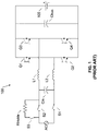
- FIG. 1 is a prior art schematic block diagram representative of a voltage converter 100 used in some charging systems installed onboard an electric vehicle to charge a high energy capacity battery assembly 105.
- circuit 100 describes a boost rectifier for an electric vehicle that includes a set of four transistors (Q1-Q4) having an output coupled to a smoothing capacitor Cbus in parallel with battery assembly 105 and an input coupled to an input filter capacitor Cin and a pair of inductors (L1 and L2).
- a pair of switches (S1 and S2) couple the inductors to an AC source, the AC source nominally providing 240 volts at about 70 amps.
- switch S1 and switch S2 are closed and S3 is open, and converter 100 operates in normal boost mode without difficulties.
- voltage converter 100 includes resistor R trickle and a switch S3. Switch S1 and switch S3 are closed and switch S2 is opened, and R trickle then reduces input voltage applied to the boost rectifier. In some implementations, one-half of the input voltage is dropped across R trickle , greatly reducing the effective voltage applied to converter 100 (with about 7 amps of charging current available in this trickle charge mode). Voltage converter 100 operates in this non-standard mode until the relative voltage conditions between AC line-in voltage and voltage level of energy storage assembly 105 is sufficient to reconfigure the converter to normal mode operation (i.e., opening switch S3 and closing switch S2).
- a further drawback of the solution shown in FIG. 1 is that there are situations in which a voltage level of the battery assembly is so low that it would be unsafe to attempt to restore function by trickle charging.
- What is needed is a voltage converter that is capable of providing high energy to a high performance energy storage assembly for charging the energy storage assembly while efficiently and safely handling conditions of a too "high" line-in voltage relative to a voltage level of the energy storage assembly while also being capable of use in reviving a battery assembly having a very low level state-of-charge.
- the present invention relates to a voltage converter according to claim 1 and a method according to claim 17.
- a voltage converter for charging an energy storage module from an alternating current line voltage includes a first charging stage, coupled to the energy storage module, converting the line voltage to a first rectified direct current module charging voltage communicated to the energy storage module, the first rectified direct current module charging voltage greater than the line voltage, the first charging stage including an inductance for communicating a first charging current to the energy storage module; a second charging stage, switchably coupled serially with the first charging stage, down-converting the alternating current line voltage to a second rectified direct current module voltage, the second rectified direct current module voltage less than the first rectified direct current module charging voltage, wherein the second charging stage produces a second charging current not greater than the first charging current; and a controller for selectably switching the second charging stage serially with the first charging stage when the line voltage has a peak value greater than a predefined relationship to a voltage of the energy storage module wherein the second charging stage communicates the second charging current to the energy storage module through the inductance.
- a power factor correcting voltage converter for charging an energy storage module from an alternating current line voltage, including a rectifier for converting the line voltage to a rectified direct current voltage provided across a first output node and a second output node; a first charging stage, coupled to the energy storage module, converting the rectified direct current voltage to a first rectified direct current module charging voltage communicated to the energy storage module, the first rectified direct current module charging voltage greater than the line voltage, the first charging stage including an inductance for communicating a first charging current to the energy storage module; a second charging stage, coupled to the outputs of the rectifier and switchably coupled serially with the first charging stage, down-converting the rectified direct current voltage to a second rectified direct current module voltage, the second rectified direct current module voltage less than the first rectified direct current module charging voltage, wherein the second charging stage produces a second charging current not greater than the first charging current; and a controller for selectably switching the second charging stage serially with the first charging stage when the line voltage has a peak value greater than a predefined
- a method for charging an energy storage module from an alternating current line voltage including (a) converting, using a first charging stage coupled to the energy storage module, the line voltage to a first rectified direct current module charging voltage communicated to the energy storage module, the first rectified direct current module charging voltage greater than the line voltage, the first charging stage including an inductance for communicating a first charging current to the energy storage module; (b) down-converting, using a second charging stage switchably coupled serially with the first charging stage, the alternating current line voltage to a second rectified direct current module voltage, the second rectified direct current module voltage less than the first rectified direct current module charging voltage, wherein the second charging stage produces a second charging current not greater than the first charging current; and (c) switching selectably the second charging stage serially with the first charging stage when the line voltage has a peak value greater than a predefined relationship to a voltage of the energy storage module wherein the second charging stage communicates the second charging current to the energy storage module through the inductance.
- a method for charging of an energy storage module from an alternating current line voltage including (a) converting the line voltage to a rectified direct current voltage provided across a first output node and a second output node; (b) converting the rectified direct current voltage to a first rectified direct current module charging voltage communicated to the energy storage module, the first rectified direct current module charging voltage greater than the line voltage, the first charging stage including an inductance for communicating a first charging current to the energy storage module; (c) down-converting the rectified direct current voltage to a second rectified direct current module voltage, the second rectified direct current module voltage less than the first rectified direct current module charging voltage, wherein the second charging stage produces a second charging current not greater than the first charging current; and (d) switching selectably the second charging stage serially with the first charging stage when the line voltage has a peak value greater than a predefined relationship to a voltage of the energy storage module wherein the second charging stage communicates the second charging current to the energy storage module through the inductance.
- the preferred embodiments of the present invention provide for a standard boost stage to up-convert line voltage to V Storage .
- a peak voltage of the line voltage exceeds the energy storage voltage (such as can happen with a low state-of-charge for an energy storage module)
- an auxiliary pole converter is switched in-line with the boost stage.
- This auxiliary pole converter down-converts the input voltage and provides a reduced charging current to the energy storage module as long as the non-standard condition exists.
- Expensive components e.g., high-energy inductance(s)
- boost stage is reconfigured as well.
- a controller disables most boosting and rectification of the boost stage in the non-standard mode operation, the specifics vary based upon the specific topology of the stages and application.
- Embodiments of the present invention provide methods and systems for a voltage converter that is capable of providing high energy to a high performance energy storage assembly for charging the energy storage assembly while efficiently and safely handling conditions of large relative differences between a line-in voltage and voltage level of the energy storage assembly while also being capable of use in reviving a energy storage assembly having a very low level state-of-charge.
- the following description is presented to enable one of ordinary skill in the art to make and use the invention and is provided in the context of a patent application and its requirements.
- the terms “energy storage assembly” “battery”, “cell”, “battery cell” and “battery cell pack” “electric double-layer capacitor” and “ultracapacitor” may be used interchangeably (unless the context indicates otherwise” and may refer to any of a variety of different rechargeable configurations and cell chemistries including, but not limited to, lithium ion (e.g., lithium iron phosphate, lithium cobalt oxide, other lithium metal oxides, etc.), lithium ion polymer, nickel metal hydride, nickel cadmium, nickel hydrogen, nickel zinc, silver zinc, or other chargeable high energy storage type/configuration.
- lithium ion e.g., lithium iron phosphate, lithium cobalt oxide, other lithium metal oxides, etc.
- lithium ion polymer e.g., nickel metal hydride, nickel cadmium, nickel hydrogen, nickel zinc, silver zinc, or other chargeable high energy storage type/configuration.
- FIG. 2 is a schematic block diagram of a bi-directional power factor correcting voltage converter 200 providing high energy to a high performance energy storage assembly 205 for charging energy storage assembly 205 while efficiently and safely handling conditions of large relative differences between a line-in voltage from an AC source 210 and a voltage level of energy storage assembly 205.
- AC source 210 e.g., 240 volts
- AC source 210 is coupled to an input of an optional EMI filter 215 having an output coupled to a switching assembly including a pair of single-pole-double-throw switches (switch S2 and switch S3).
- a first output port of EMI filter 215 is coupled to a first throw of switch S2 and a second output port of EMI filter 215 is coupled to a first throw of switch S3.
- the switching assembly responsive to its state, couples either (i) filtered line voltage from AC source 210 to a boost rectifier 220 or (ii) an auxiliary pole converter 225 to a modified boost rectifier 220.
- a second throw of switch S2 and of switch S3 are coupled to auxiliary pole converter 225 and the first poles of switch S2 and of switch S3 are coupled to boost rectifier 220.
- the switching assembly communicates the filtered line voltage from AC source 210 to boost rectifier 220 and then to energy storage assembly 205 to provide a standard charging current, for example a charging current of about 70 amps.
- the switching assembly does this by coupling the poles of switch S2 and of switch S3 to the first throws, respectively.
- the switching assembly disconnects EMI filter 215 from direct communication with boost rectifier 220 and communicates auxiliary pole converter 225 to energy storage assembly 205 through a modified boost rectifier 220.
- Auxiliary converter 225 provides a "trickle' current (the trickle current may have substantial amps but is less than or equal to the standard charging current), for example in the preferred embodiment the trickle current is about 35 amps in contrast to a standard charging current of 70 amps.
- the switching assembly does this by coupling the poles of switch S2 and of switch S3 to the second throws, respectively.
- a controller 230 sets the desired states and operation for the switches, transistors, and components of converter 200 as described herein.
- Boost rectifier 220 may be constructed in various ways, a preferred implementation is shown in FIG. 2 .
- Boost rectifier 220 of the preferred implementation includes a pair of high current inductances (L1 and L2 - though this implementation may be accomplished with a single inductance) having first nodes coupled to a pole of switch S2 and switch S3 respectively and second nodes coupled to a full rectifying bridge having four NPN insulated gate bipolar transistors Q1-Q4 (IGBTs) and a smoothing capacitor C bus .
- IGBTs NPN insulated gate bipolar transistors
- EMI filter 215 has a first output port coupled to a first throw of switch S2.
- the second node of inductance L1 is coupled to an emitter of transistor Q3 and a collector of transistor Q4.
- EMI filter 215 has a second output port coupled to a first throw of switch S3.
- the second node of inductance L2 is coupled to an emitter of transistor Q1 and a collector of transistor Q2.
- the collectors of transistor Q1 and transistor Q3 are coupled to a first plate of smoothing capacitor C bus and a first terminal of energy storage assembly 205.
- the emitters of transistor Q2 and transistor Q4 are coupled to a second plate of smoothing capacitor C bus and to a second terminal of energy storage assembly 205.
- the components of boost rectifier 220 are sized for very high current levels, such as for example, currents used in charging the energy storage modules of an electric vehicle or other automotive or industrial application. As indicated above, these currents may be on the order of about 70 amps in the preferred embodiment.
- Controller 230 detects this voltage condition and reconfigures converter 200 by switching in auxiliary pole converter 225 and modifying operation of boost rectifier 220.
- auxiliary pole converter 225 is switched in at the correct location to reuse inductances L1 and L2 which requires reconfiguration of transistors Q1-Q4 as well to disable rectification and boosting in boost rectifier 220.
- Auxiliary pole converter 225 includes a rectifier 235, an NPN IGBT Q t , a diode D t , and a filter capacitor C t .
- controller 230 statically turns transistor Q2 and Q3 to the "ON" state.
- a first input port of rectifier 235 is coupled to the first output port of EMI filter 215 and a second input port of rectifier 235 is coupled to the second output port of EMI filter 215.
- a first rectified voltage node of rectifier 235 is coupled to a first plate of filter capacitor C t and to a collector of transistor Q t .
- a second rectified voltage node of rectifier 235 is coupled to a second plate of filter capacitor C t , to an anode of diode D t , and to a second throw of switch S3.
- a cathode of diode D t is coupled to an emitter of transistor Q t and to a second throw of switch S2.
- Converter 200 controls current by switching transistor Q t .
- Components of auxiliary pole converter 225 are advantageously sized to be larger and supply a greater auxiliary trickle current than that provided by the prior art, in a more efficient manner, but still less charging current than the standard charging current.
- the preferred implementation sizes the components of auxiliary pole converter 225 to provide about 35 amps of trickle current efficiently in contrast to the 7 amps provided by the prior art in a lossy manner.
- the efficiencies of the present invention include less energy lost through heat and less time spent in the trickle charge mode, resulting in a doubly efficient solution.
- the more often that auxiliary pole converter 225 is needed the greater the advantages of using the present invention, particularly in the high-performance automotive and industrial applications using high-performance energy storage modules.
- Rectifier 220 does implement power factor correction in standard mode (it can do power factor correction in standard mode but it will not do power factor correction in auxiliary mode).
- power factor correction may not be a requirement, particularly as the non-standard charge situation addressed by auxiliary pole converter 225 is expected to be a temporary transient condition, and because of the present design providing significantly greater trickle currents, the time that the auxiliary pole is switched is greatly reduced. However, for some applications power factor correction may be required or desired.
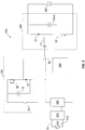
- FIG. 3 s a schematic block diagram of a power factor correcting voltage converter 300 providing high energy to a high performance energy storage assembly 305 for charging energy storage assembly 305 while efficiently and safely handling conditions of large relative differences between a line-in voltage from an AC source 310 and a voltage level of energy storage assembly 305.
- AC source 310 e.g., 240 volts
- Rectifier 320 includes a first rectified voltage node which is coupled to a first throw of a single pole, double throw switch S2.
- the pole of switch S2 is coupled to a converter stage 325 and a second throw of switch S2 is couple to an auxiliary pole converter 330.
- one or more of the switches will be implemented by one or more contactors (e.g., relays or the like).
- the pole of switch S2 is coupled to the first throw which communicates the filtered rectified line voltage from AC source 310 to converter stage 325 and then to energy storage assembly 305.
- switch S2 communicates auxiliary pole converter 330 to energy storage assembly 305 through a modified converter stage 325 by coupling the pole of switch S2 to the second throw.
- Auxiliary converter 330 provides a "trickle' current (the trickle current may have substantial amps but is less than or equal to the standard charging current), for example in the preferred embodiment the trickle current is about 35 amps in contrast to a standard charging current of 70 amps.
- a controller 335 sets the desired states and operation for the switches, transistors, and components of converter 300.
- Converter stage 325 may be constructed in various ways, a preferred implementation is shown in FIG. 3 .
- Converter stage 325 of the preferred implementation includes a high current inductance L1 having a first node coupled to a pole of switch S2 and a second node coupled to both an anode of a diode D1 and to a collector of an NPN IGBT Q1.
- a cathode of diode D1 is coupled to a first plate of a smoothing capacitor C bus and a first terminal of energy storage assembly 305.
- An emitter of transistor Q1 is coupled to a second rectified voltage node of rectifier 320, a second plate of smoothing capacitor C bus and a second terminal of energy storage assembly 305.
- the components of converter stage 325 are sized for very high current levels, such as for example, currents used in charging the energy storage modules of an electric vehicle or other automotive or industrial application. As indicated above, these currents may be on the order of about 70 amps in the preferred embodiment.
- Controller 335 detects this condition and reconfigures converter 300 by switching in auxiliary pole converter 330 (changing throws of switch S2 and closing switch S3) and reconfiguring operation of converter stage 325.
- auxiliary pole converter 330 is switched in at the correct location to reuse rectifier 320 and inductance L1 and controller 335 statically turns transistor Q1 "OFF" which puts diode D1 in series with inductance L1 (and disables boosting of converter stage 325).
- Auxiliary pole converter 330 includes an NPN IGBT Q t , a diode D t , and a filter capacitor C t .
- a first terminal of a single pole single throw switch S3 is coupled to the first rectified voltage node of rectifier 320.
- a second terminal of switch S3 is coupled to a first plate of filter capacitor C t and to a collector of transistor Q t .
- a second plate of filter capacitor C t is coupled to the second rectified voltage node of rectifier 320 and to an anode of diode D t .
- a cathode of diode D t is coupled to an emitter of transistor Q t and to a second throw of switch S2.
- auxiliary pole converter 330 When auxiliary pole converter 330 is switched in, controller 335 statically turns Q1 to the "OFF" state.
- Converter 300 controls current in the special mode as auxiliary converter 330 acts as a buck converter reducing the line in voltage.
- Components of auxiliary pole converter 330 are advantageously sized to be larger and supply a greater auxiliary trickle current than that provided by the prior art, in a more efficient manner, but still less than or equal to the standard charging current.
- the preferred implementation sizes the components of auxiliary pole converter 330 to provide about 35 amps of trickle current efficiently in contrast to the 7 amps provided by the prior art in a lossy manner.
- the efficiencies of the present invention include less energy lost through heat and less time spent in the trickle charge mode, resulting in a doubly efficient solution.
- the voltage level from the auxiliary pole converters may be bucked down sufficiently low that the auxiliary pole converter voltages from converter 200 and converter 300 may be used in safely reviving a damaged battery module.
- the prior art is unable to provide a safe voltage for recharging such a battery module using the voltage drop across a resistor.
Landscapes
- Engineering & Computer Science (AREA)
- Power Engineering (AREA)
- Charge And Discharge Circuits For Batteries Or The Like (AREA)
- Dc-Dc Converters (AREA)
Claims (20)
- Spannungswandler (200) zum Laden eines Energiespeichermoduls (205) aus einer Netz-Wechselspannung, umfassend:eine erste Ladestufe (220), die mit dem Energiespeichermodul (205) gekoppelt ist, zum Umwandeln der Netzspannung in eine erste gleichgerichtete Gleichstrommodul-Ladespannung, die an das Energiespeichermodul (205) übertragen wird, wobei die erste gleichgerichtete Gleichstrommodul-Ladespannung größer ist als die Netzspannung, wobei die erste Ladestufe (220) eine Induktivität (L1, L2) zum Übertragen eines ersten Ladestroms an das Energiespeichermodul (205) umfasst;eine zweite Ladestufe (225), die mit der ersten Ladestufe (220) schaltbar in Reihe geschaltet ist und die Netz-Wechselspannung in eine zweite gleichgerichtete Gleichstrommodul-Spannung abwärts wandelt, wobei die zweite gleichgerichtete Gleichstrommodul-Spannung kleiner ist als die erste gleichgerichtete Gleichstrommodul-Ladespannung, wobei die zweite Ladestufe (225) einen zweiten Ladestrom erzeugt, der nicht größer ist als der erste Ladestrom, und eine Steuereinrichtung (230) zum selektiven Schalten der zweiten Ladestufe (225) in Reihe mit der ersten Ladestufe (220), wobeidie Steuereinrichtung (230) dazu eingerichtet ist, die zweite Ladestufe (225) selektiv mit der ersten Ladestufe (220) in Reihe zu schalten, wenn die Netzspannung einen Spitzenwert hat, der größer ist als eine vorgegebene Beziehung zu einer Spannung des Energiespeichermoduls (205), wobei die zweite Ladestufe (225) den zweiten Ladestrom an das Energiespeichermodul (205) über die Induktivität (L1, L2) überträgt.
- Spannungswandler nach Anspruch 1, wobei die erste Ladestufe (220) ein Boost-Gleichrichter umfasst, wobei die Induktivität eine erste Induktivität (L1) und eine zweite Induktivität (L2) aufweist und die Induktivitäten mit der Netzspannung gekoppelt sind, und wobei der Boost-Gleichrichter einen aktiven Vollweggleichrichter (Q1-Q4) umfasst, der einen ersten Eingang, der über die erste Induktivität (L1) mit der Netzspannung gekoppelt ist, einen zweiten Eingang, der über die zweite Induktivität (L2) mit der Netzspannung gekoppelt ist, einen ersten Ausgang, der mit einem ersten Anschluss des Energiespeichermoduls (205) gekoppelt ist, und einen zweiten Ausgang, der mit einem zweiten Anschluss des Energiespeichermoduls (205) gekoppelt ist, aufweist.
- Spannungswandler nach Anspruch 1, wobei die zweite Ladestufe (225) einen Hilfspolwandler aufweist, wobei die Induktivität eine erste Induktivität (L1) und eine zweite Induktivität (L2) umfasst und wobei der Hilfspolwandler einen Gleichrichter (235) und einen Abwärtsspannungswandler umfasst, der die zweite gleichgerichtete Gleichstrommodul-Spannung erzeugt, wobei der Hilfspolwandler den zweiten Ladestrom an das Energiespeichermodul (205) über die Induktivitäten (L1, L2) bereitstellt.
- Spannungswandler nach Anspruch 2, wobei die zweite Ladestufe (225) einen Hilfspolwandler umfasst und wobei der Hilfspolwandler einen zweiten Gleichrichter (235) und einen Abwärtsspannungswandler umfasst, der die zweite gleichgerichtete Gleichstrommodul-Spannung erzeugt, wobei der Hilfspolwandler (225) den zweiten Ladestrom an das Energiespeichermodul (205) über die Induktivitäten (L1, L2) liefert, wenn die Induktivitäten (L1, L2) mit der Netzspannung über den Gleichrichter (235) des Hilfspolwandlers verbunden sind.
- Spannungswandler nach Anspruch 4, wobei die Steuereinrichtung die Gleichrichtung durch den Boost-Gleichrichter (Q1-Q4) sperrt, wenn der Hilfspolwandler den zweiten Ladestrom über die Induktivitäten (L1, L2) bereitstellt.
- Spannungswandler nach Anspruch 1, wobei die vorgegebene Beziehung für die Netzspannung in dem Bereich von ungefähr 85% bis ungefähr 99,9% der Spannung des Energiespeichermoduls (205) liegt.
- Spannungswandler nach Anspruch 3, wobei der Abwärtsspannungswandler einen Buck-Wandler umfasst.
- Spannungswandler nach Anspruch 4, wobei der Abwärtsspannungswandler einen Buck-Wandler umfasst.
- Kompensations-Spannungswandler zum Laden eines Energiespeichermoduls (305) aus einer Netz-Wechselspannung, umfassend:ein Gleichrichter (302) zum Umwandeln der Netzspannung in eine gleichgerichtete Gleichspannung, die über einem ersten Ausgangsknoten und einem zweiten Ausgangsknoten bereitgestellt wird;eine erste Ladestufe (325), die mit dem Energiespeichermodul (305) gekoppelt ist, zum Umwandeln der gleichgerichteten Gleichspannung in eine erste gleichgerichtete Gleichstrommodul-Ladespannung, die an das Energiespeichermodul (305) übertragen wird, wobei die erste gleichgerichtete Gleichstrommodul-Ladespannung größer ist als die Netzspannung, wobei die erste Ladestufe eine Induktivität (L1) zum Übertragen eines ersten Ladestroms an das Energiespeichermodul (305) umfasst;eine zweite Ladestufe (330), die mit den Ausgängen des Gleichrichters (320) gekoppelt und mit der ersten Ladestufe (325) schaltbar in Reihe geschaltet ist und die gleichgerichtete Gleichspannung in eine zweite gleichgerichtete Gleichstrommodul-Spannung abwärts wandelt, wobei die zweite gleichgerichtete Gleichstrommodul-Spannung kleiner ist als die erste gleichgerichtete Gleichstrommodul-Ladespannung, wobei die zweite Ladestufe (330) einen zweiten Ladestrom erzeugt, der nicht größer ist als der erste Ladestrom, und eine Steuereinrichtung (335) zum selektiven Schalten der zweiten Ladestufe (330) in Reihe mit der ersten Ladestufe (325), wobeidie Steuereinrichtung (335) dazu eingerichtet ist, die zweite Ladestufe (330) mit der ersten Ladestufe (325) selektiv in Reihe zu schalten, wenn die Netzspannung einen Spitzenwert hat, der größer ist als eine vorgegebene Beziehung zu einer Spannung des Energiespeichermoduls (305), wobei die zweite Ladestufe (330) den zweiten Ladestrom an das Energiespeichermodul (305) über die Induktivität (L1) überträgt.
- Spannungswandler nach Anspruch 9, wobei die erste Ladestufe (325) ein Boost-Gleichrichter umfasst, wobei die Induktivität (L1) mit der gleichgerichteten Gleichspannung gekoppelt ist, und wobei der Boost-Gleichrichter einen ersten Eingang, der über die erste Induktivität (L1) mit dem Gleichrichter(320) gekoppelt ist, einen zweiten Eingang, der mit dem Gleichrichter (320) gekoppelt ist, einen ersten Ausgang, der mit einem ersten Anschluss des Energiespeichermoduls (305) gekoppelt ist, und einen zweiten Ausgang, der mit einem zweiten Anschluss des Energiespeichermoduls (305) gekoppelt ist, aufweist.
- Spannungswandler nach Anspruch 9, wobei die zweite Ladestufe (320) einen Hilfspolwandler aufweist, der einen Abwärtsspannungswandler umfasst, der die zweite gleichgerichtete Gleichstrommodul-Spannung erzeugt, wobei der Hilfspolwandler den zweiten Ladestrom an das Energiespeichermodul (305) über die Induktivität (L1) bereitstellt.
- Spannungswandler nach Anspruch 10, wobei die zweite Ladestufe (330) einen Hilfspolwandler umfasst, der einen Abwärtsspannungswandler aufweist, der die zweite gleichgerichtete Gleichstrommodul-Spannung erzeugt, wobei der Hilfspolwandler den zweiten Ladestrom an das Energiespeichermodul (305) über die Induktivität (L1) liefert.
- Spannungswandler nach Anspruch 12, wobei die Steuereinrichtung (320) das Spannungs-Boosting durch den Boost-Gleichrichter sperrt, wenn der Hilfspolwandler den zweiten Ladestrom über die Induktivität (L1) bereitstellt.
- Spannungswandler nach Anspruch 9, wobei die vorgegebene Beziehung für die Netzspannung in dem Bereich von ungefähr 85% bis ungefähr 99,9% der Spannung des Energiespeichermoduls (305) liegt.
- Spannungswandler nach Anspruch 11, wobei der Abwärtsspannungswandler einen Buck-Wandler umfasst.
- Spannungswandler nach Anspruch 12, wobei der Abwärtsspannungswandler einen Buck-Wandler umfasst.
- Verfahren zum Laden eines Energiespeichermoduls (205) aus einer Netz-Wechselspannung, umfassend:(a) Umwandeln der Netzspannung in eine erste gleichgerichtete Gleichstrommodul-Ladespannung, die an ein Energiespeichermodul (205) übertragen wird, unter Verwendung einer ersten Ladestufe (220), die mit dem Energiespeichermodul (205) gekoppelt ist, wobei die erste gleichgerichtete Gleichstrommodul-Ladespannung größer ist als die Netzspannung, wobei die erste Ladestufe (220) eine Induktivität (L1, L2) zur Übertragung eines ersten Ladestroms an das Energiespeichermoduls (205) umfasst; und(b) Abwärtswandeln der Netz-Wechselspannung auf eine zweite gleichgerichtete Gleichstrommodul-Spannung unter Verwendung einer zweiten Ladestufe (225), die mit der ersten Ladestufe (220) schaltbar in Reihe geschaltet ist, wobei die zweite gleichgerichtete Gleichstrommodul-Spannung geringer ist als die erste gleichgerichtete Gleichstrommodul-Ladespannung, wobei die zweite Ladestufe (225) einen zweiten Ladestrom erzeugt, der nicht größer ist als der erste Ladestrom, und(c) Selektives Schalten der zweiten Ladestufe (225) in Reihe mit der ersten Ladestufe (220), wenn die Netzspannung einen Spitzenwert hat, der größer ist als eine vorgegebene Beziehung zu einer Spannung des Energiespeichermoduls (205), wobei die zweite Ladestufe (225) den zweiten Ladestrom an das Energiespeichermodul (205) über die Induktivität (L1, L2) überträgt.
- Ladeverfahren nach Anspruch 17, wobei das wahlweise Schalten (c) die Gleichrichtung und das Spannungs-Boosting der ersten Ladestufe (220) sperrt.
- Verfahren zum Laden eines Energiespeichermoduls (305) aus einer Netz-Wechselspannung, umfassend:(a) Umwandeln der Netzspannung in eine gleichgerichtete Gleichspannung, die über einen ersten Ausgangsknoten und einem zweiten Ausgangsknoten bereitgestellt wird;(b) Umwandeln der gleichgerichteten Gleichspannung in eine erste gleichgerichtete Gleichstrommodul-Ladespannung, die an das Energiespeichermodul (305) übertragen wird, wobei die erste gleichgerichtete Gleichstrommodul-Ladespannung größer ist als die Netzspannung, wobei eine erste Ladestufe (325) eine Induktivität (L1) zum Übertragen eines ersten Ladestroms an das Energiespeichermodul (305) aufweist; und(c) Abwärtswandeln der gleichgerichteten Gleichspannung auf eine zweite gleichgerichtete Gleichstrommodul-Spannung, wobei die zweite gleichgerichtete Gleichstrommodul-Spannung geringer ist als die erste gleichgerichtete Gleichstrommodul-Spannung, wobei eine zweite Ladestufe (330) einen zweiten Ladestrom erzeugt, der nicht größer ist als der erste Ladestrom, und(d) Wahlweises Schalten der zweiten Ladestufe (330) in Reihe mit der ersten Ladestufe (325), wenn die Netzspannung einen Spitzenwert hat, der größer ist als eine vorgegebene Beziehung zu einer Spannung des Energiespeichermoduls (305), wobei die zweite Ladestufe (330) den zweiten Ladestrom an das Energiespeichermodul (305) über die Induktivität (L1) überträgt.
- Ladeverfahren nach Anspruch 19, wobei das wahlweise Schalten (d) das Spannungs-Boosting der ersten Ladestufe sperrt.
Applications Claiming Priority (1)
| Application Number | Priority Date | Filing Date | Title |
|---|---|---|---|
| US12/763,029 US8324863B2 (en) | 2010-04-19 | 2010-04-19 | Trickle charger for high-energy storage systems |
Publications (3)
| Publication Number | Publication Date |
|---|---|
| EP2378622A2 EP2378622A2 (de) | 2011-10-19 |
| EP2378622A3 EP2378622A3 (de) | 2014-12-10 |
| EP2378622B1 true EP2378622B1 (de) | 2018-08-08 |
Family
ID=44117087
Family Applications (1)
| Application Number | Title | Priority Date | Filing Date |
|---|---|---|---|
| EP11003292.7A Active EP2378622B1 (de) | 2010-04-19 | 2011-04-19 | Erhaltungsladegerät für Hochenergiespeichersysteme |
Country Status (3)
| Country | Link |
|---|---|
| US (1) | US8324863B2 (de) |
| EP (1) | EP2378622B1 (de) |
| CN (1) | CN102223092B (de) |
Families Citing this family (9)
| Publication number | Priority date | Publication date | Assignee | Title |
|---|---|---|---|---|
| DE102010042328A1 (de) * | 2010-10-12 | 2012-04-12 | Robert Bosch Gmbh | Verfahren zum Überwachen des Ladebetriebs eines Energiespeichers in einem Fahrzeug und Ladesystem zum Laden eines Energiespeichers in einem Fahrzeug |
| US9887619B2 (en) * | 2014-06-23 | 2018-02-06 | Infineon Technologies Austria Ag | System and method for a normally-on switched mode power supply |
| US9642276B2 (en) | 2014-12-01 | 2017-05-02 | Tesla, Inc. | Welding and soldering of transistor leads |
| FR3035282B1 (fr) * | 2015-04-15 | 2018-05-11 | Valeo Siemens Eautomotive France Sas | Chargeur de batterie, installation electrique et vehicule automobile |
| CN106891740B (zh) * | 2015-12-18 | 2019-12-20 | 比亚迪股份有限公司 | 电动汽车及其车载充电器和车载充电器的控制方法 |
| US10756632B2 (en) * | 2017-06-26 | 2020-08-25 | Bel Fuse (Macao Commerical Offshore) Limited | Power supply with auxiliary converter for extended input voltage range |
| KR102530939B1 (ko) * | 2018-04-09 | 2023-05-11 | 현대자동차주식회사 | 차량용 전력변환 시스템 |
| US10998730B1 (en) | 2019-04-26 | 2021-05-04 | NeoVolta, Inc. | Adaptive solar power battery storage system |
| DE102020104732A1 (de) | 2020-02-24 | 2021-08-26 | Bayerische Motoren Werke Aktiengesellschaft | EMV-Baugruppe für ein elektrisch angetriebenes Fahrzeug |
Family Cites Families (13)
| Publication number | Priority date | Publication date | Assignee | Title |
|---|---|---|---|---|
| US4536696A (en) * | 1983-07-14 | 1985-08-20 | At&T Bell Laboratories | Buck-boost converter with dual-mode control for battery charging |
| FR2573257B1 (fr) * | 1984-11-13 | 1987-01-02 | Thomson Csf | Circuit de protection contre les coupures d'alimentation electrique |
| US5642027A (en) * | 1992-01-07 | 1997-06-24 | Windes; John A. | Current-limited system for capacitive load powering |
| US5500579A (en) * | 1995-01-03 | 1996-03-19 | Motorola, Inc. | Electric motor control with integral battery charger |
| US5712549A (en) * | 1995-03-07 | 1998-01-27 | Tenergy L.L.C. | DC Motor drive assembly having a controller/charge with regenerative braking |
| US6600292B2 (en) * | 1995-08-24 | 2003-07-29 | Ellen James | Power controller utilizing power factor correction |
| JP3607033B2 (ja) * | 1997-03-31 | 2005-01-05 | 三菱電機株式会社 | 半導体装置 |
| US6628011B2 (en) * | 2000-07-28 | 2003-09-30 | International Power System, Inc. | DC to DC converter and power management system |
| JP3742780B2 (ja) * | 2002-05-09 | 2006-02-08 | 松下電器産業株式会社 | Dc−dcコンバータ |
| CN1864319A (zh) * | 2003-10-01 | 2006-11-15 | 国际整流器公司 | 单周控制的无桥路升压(blb)功率因数校正电路结构 |
| CN101431250A (zh) * | 2007-11-06 | 2009-05-13 | 上海辰蕊微电子科技有限公司 | 用于电池充电器的充电管理控制电路及其控制方法 |
| CN101436078B (zh) * | 2007-11-15 | 2011-07-13 | 深圳迈瑞生物医疗电子股份有限公司 | 宽范围调压电路及宽范围调压的实现方法 |
| US7977921B2 (en) * | 2008-08-15 | 2011-07-12 | National Semiconductor Corporation | AC-to-DC voltage conversion and charging circuitry |
-
2010
- 2010-04-19 US US12/763,029 patent/US8324863B2/en active Active
-
2011
- 2011-04-18 CN CN201110111299.4A patent/CN102223092B/zh active Active
- 2011-04-19 EP EP11003292.7A patent/EP2378622B1/de active Active
Non-Patent Citations (1)
| Title |
|---|
| None * |
Also Published As
| Publication number | Publication date |
|---|---|
| US8324863B2 (en) | 2012-12-04 |
| CN102223092B (zh) | 2015-02-25 |
| CN102223092A (zh) | 2011-10-19 |
| US20110254512A1 (en) | 2011-10-20 |
| EP2378622A3 (de) | 2014-12-10 |
| EP2378622A2 (de) | 2011-10-19 |
Similar Documents
| Publication | Publication Date | Title |
|---|---|---|
| EP2378622B1 (de) | Erhaltungsladegerät für Hochenergiespeichersysteme | |
| US12294232B2 (en) | Portable power supply | |
| EP2413452B1 (de) | Bidirektionaler polyphasen-multimodewandler, der hochsetz- und tiefsetz-hochsetz-modi umfasst | |
| Kuperman et al. | Battery charger for electric vehicle traction battery switch station | |
| US10720787B2 (en) | Combined charger and power converter | |
| US8933661B2 (en) | Integrated inductive and conductive electrical charging system | |
| EP3123604B1 (de) | Gleichstromwandler und elektrisches speichersystem | |
| EP2819291A1 (de) | Stromversorgungsvorrichtung und steuerverfahren dafür | |
| JP2012034488A (ja) | 充電装置 | |
| US12132341B2 (en) | Battery charging and discharging circuit | |
| CN106080243A (zh) | 电动车电气系统及供电方法 | |
| US20160197498A1 (en) | Device for balancing the charge of the elements of a power battery | |
| CN205945204U (zh) | 一种组合式应急保障电源 | |
| KR20220029522A (ko) | 단일단 교류 직류 변환기 | |
| US10833352B2 (en) | Vehicle having a lithium-ion battery | |
| US11837952B2 (en) | Three-phase AC to DC power converter | |
| CN102118016A (zh) | 一种充电器保护电路、含有该电路的充电器及其控制方法 | |
| Pal et al. | Power electronics—EV battery charging | |
| KR20190092994A (ko) | 차량용 배터리 충전 장치 | |
| WO2017181921A1 (zh) | 瞬态动力功率补偿器、组合式超级电池及补偿供电方法 | |
| Salari et al. | A new multiple input bidirectional HEV battery charger | |
| Varshney et al. | AC-DC PFC-CUK FED One-Switch Resonant Converter with BMS for E-Bike Battery Charging System | |
| CN105680544A (zh) | 瞬态动力功率补偿器及补偿供电方法 | |
| CN223124643U (zh) | 一种电驱动总成及电动汽车 | |
| CN110768342B (zh) | 储能设备和充放电系统 |
Legal Events
| Date | Code | Title | Description |
|---|---|---|---|
| AK | Designated contracting states |
Kind code of ref document: A2 Designated state(s): AL AT BE BG CH CY CZ DE DK EE ES FI FR GB GR HR HU IE IS IT LI LT LU LV MC MK MT NL NO PL PT RO RS SE SI SK SM TR |
|
| AX | Request for extension of the european patent |
Extension state: BA ME |
|
| PUAI | Public reference made under article 153(3) epc to a published international application that has entered the european phase |
Free format text: ORIGINAL CODE: 0009012 |
|
| REG | Reference to a national code |
Ref country code: DE Ref legal event code: R079 Ref document number: 602011050726 Country of ref document: DE Free format text: PREVIOUS MAIN CLASS: H02J0007000000 Ipc: H02M0001420000 |
|
| PUAL | Search report despatched |
Free format text: ORIGINAL CODE: 0009013 |
|
| AK | Designated contracting states |
Kind code of ref document: A3 Designated state(s): AL AT BE BG CH CY CZ DE DK EE ES FI FR GB GR HR HU IE IS IT LI LT LU LV MC MK MT NL NO PL PT RO RS SE SI SK SM TR |
|
| AX | Request for extension of the european patent |
Extension state: BA ME |
|
| RIC1 | Information provided on ipc code assigned before grant |
Ipc: H02J 7/02 20060101ALI20141104BHEP Ipc: H02M 1/42 20070101AFI20141104BHEP |
|
| 17P | Request for examination filed |
Effective date: 20150408 |
|
| RBV | Designated contracting states (corrected) |
Designated state(s): AL AT BE BG CH CY CZ DE DK EE ES FI FR GB GR HR HU IE IS IT LI LT LU LV MC MK MT NL NO PL PT RO RS SE SI SK SM TR |
|
| GRAP | Despatch of communication of intention to grant a patent |
Free format text: ORIGINAL CODE: EPIDOSNIGR1 |
|
| STAA | Information on the status of an ep patent application or granted ep patent |
Free format text: STATUS: GRANT OF PATENT IS INTENDED |
|
| INTG | Intention to grant announced |
Effective date: 20171011 |
|
| GRAJ | Information related to disapproval of communication of intention to grant by the applicant or resumption of examination proceedings by the epo deleted |
Free format text: ORIGINAL CODE: EPIDOSDIGR1 |
|
| STAA | Information on the status of an ep patent application or granted ep patent |
Free format text: STATUS: REQUEST FOR EXAMINATION WAS MADE |
|
| INTC | Intention to grant announced (deleted) | ||
| RAP1 | Party data changed (applicant data changed or rights of an application transferred) |
Owner name: TESLA, INC. |
|
| RAP1 | Party data changed (applicant data changed or rights of an application transferred) |
Owner name: TESLA, INC. |
|
| GRAR | Information related to intention to grant a patent recorded |
Free format text: ORIGINAL CODE: EPIDOSNIGR71 |
|
| GRAS | Grant fee paid |
Free format text: ORIGINAL CODE: EPIDOSNIGR3 |
|
| STAA | Information on the status of an ep patent application or granted ep patent |
Free format text: STATUS: GRANT OF PATENT IS INTENDED |
|
| GRAA | (expected) grant |
Free format text: ORIGINAL CODE: 0009210 |
|
| STAA | Information on the status of an ep patent application or granted ep patent |
Free format text: STATUS: THE PATENT HAS BEEN GRANTED |
|
| INTG | Intention to grant announced |
Effective date: 20180627 |
|
| AK | Designated contracting states |
Kind code of ref document: B1 Designated state(s): AL AT BE BG CH CY CZ DE DK EE ES FI FR GB GR HR HU IE IS IT LI LT LU LV MC MK MT NL NO PL PT RO RS SE SI SK SM TR |
|
| REG | Reference to a national code |
Ref country code: GB Ref legal event code: FG4D |
|
| REG | Reference to a national code |
Ref country code: CH Ref legal event code: EP Ref country code: AT Ref legal event code: REF Ref document number: 1028127 Country of ref document: AT Kind code of ref document: T Effective date: 20180815 |
|
| REG | Reference to a national code |
Ref country code: IE Ref legal event code: FG4D |
|
| REG | Reference to a national code |
Ref country code: DE Ref legal event code: R096 Ref document number: 602011050726 Country of ref document: DE |
|
| REG | Reference to a national code |
Ref country code: NL Ref legal event code: MP Effective date: 20180808 |
|
| REG | Reference to a national code |
Ref country code: LT Ref legal event code: MG4D |
|
| REG | Reference to a national code |
Ref country code: AT Ref legal event code: MK05 Ref document number: 1028127 Country of ref document: AT Kind code of ref document: T Effective date: 20180808 |
|
| PG25 | Lapsed in a contracting state [announced via postgrant information from national office to epo] |
Ref country code: FI Free format text: LAPSE BECAUSE OF FAILURE TO SUBMIT A TRANSLATION OF THE DESCRIPTION OR TO PAY THE FEE WITHIN THE PRESCRIBED TIME-LIMIT Effective date: 20180808 Ref country code: SE Free format text: LAPSE BECAUSE OF FAILURE TO SUBMIT A TRANSLATION OF THE DESCRIPTION OR TO PAY THE FEE WITHIN THE PRESCRIBED TIME-LIMIT Effective date: 20180808 Ref country code: AT Free format text: LAPSE BECAUSE OF FAILURE TO SUBMIT A TRANSLATION OF THE DESCRIPTION OR TO PAY THE FEE WITHIN THE PRESCRIBED TIME-LIMIT Effective date: 20180808 Ref country code: RS Free format text: LAPSE BECAUSE OF FAILURE TO SUBMIT A TRANSLATION OF THE DESCRIPTION OR TO PAY THE FEE WITHIN THE PRESCRIBED TIME-LIMIT Effective date: 20180808 Ref country code: NL Free format text: LAPSE BECAUSE OF FAILURE TO SUBMIT A TRANSLATION OF THE DESCRIPTION OR TO PAY THE FEE WITHIN THE PRESCRIBED TIME-LIMIT Effective date: 20180808 Ref country code: LT Free format text: LAPSE BECAUSE OF FAILURE TO SUBMIT A TRANSLATION OF THE DESCRIPTION OR TO PAY THE FEE WITHIN THE PRESCRIBED TIME-LIMIT Effective date: 20180808 Ref country code: GR Free format text: LAPSE BECAUSE OF FAILURE TO SUBMIT A TRANSLATION OF THE DESCRIPTION OR TO PAY THE FEE WITHIN THE PRESCRIBED TIME-LIMIT Effective date: 20181109 Ref country code: IS Free format text: LAPSE BECAUSE OF FAILURE TO SUBMIT A TRANSLATION OF THE DESCRIPTION OR TO PAY THE FEE WITHIN THE PRESCRIBED TIME-LIMIT Effective date: 20181208 Ref country code: PL Free format text: LAPSE BECAUSE OF FAILURE TO SUBMIT A TRANSLATION OF THE DESCRIPTION OR TO PAY THE FEE WITHIN THE PRESCRIBED TIME-LIMIT Effective date: 20180808 Ref country code: NO Free format text: LAPSE BECAUSE OF FAILURE TO SUBMIT A TRANSLATION OF THE DESCRIPTION OR TO PAY THE FEE WITHIN THE PRESCRIBED TIME-LIMIT Effective date: 20181108 Ref country code: BG Free format text: LAPSE BECAUSE OF FAILURE TO SUBMIT A TRANSLATION OF THE DESCRIPTION OR TO PAY THE FEE WITHIN THE PRESCRIBED TIME-LIMIT Effective date: 20181108 |
|
| PG25 | Lapsed in a contracting state [announced via postgrant information from national office to epo] |
Ref country code: AL Free format text: LAPSE BECAUSE OF FAILURE TO SUBMIT A TRANSLATION OF THE DESCRIPTION OR TO PAY THE FEE WITHIN THE PRESCRIBED TIME-LIMIT Effective date: 20180808 Ref country code: HR Free format text: LAPSE BECAUSE OF FAILURE TO SUBMIT A TRANSLATION OF THE DESCRIPTION OR TO PAY THE FEE WITHIN THE PRESCRIBED TIME-LIMIT Effective date: 20180808 Ref country code: LV Free format text: LAPSE BECAUSE OF FAILURE TO SUBMIT A TRANSLATION OF THE DESCRIPTION OR TO PAY THE FEE WITHIN THE PRESCRIBED TIME-LIMIT Effective date: 20180808 Ref country code: ES Free format text: LAPSE BECAUSE OF FAILURE TO SUBMIT A TRANSLATION OF THE DESCRIPTION OR TO PAY THE FEE WITHIN THE PRESCRIBED TIME-LIMIT Effective date: 20180808 |
|
| PG25 | Lapsed in a contracting state [announced via postgrant information from national office to epo] |
Ref country code: EE Free format text: LAPSE BECAUSE OF FAILURE TO SUBMIT A TRANSLATION OF THE DESCRIPTION OR TO PAY THE FEE WITHIN THE PRESCRIBED TIME-LIMIT Effective date: 20180808 Ref country code: CZ Free format text: LAPSE BECAUSE OF FAILURE TO SUBMIT A TRANSLATION OF THE DESCRIPTION OR TO PAY THE FEE WITHIN THE PRESCRIBED TIME-LIMIT Effective date: 20180808 Ref country code: RO Free format text: LAPSE BECAUSE OF FAILURE TO SUBMIT A TRANSLATION OF THE DESCRIPTION OR TO PAY THE FEE WITHIN THE PRESCRIBED TIME-LIMIT Effective date: 20180808 Ref country code: IT Free format text: LAPSE BECAUSE OF FAILURE TO SUBMIT A TRANSLATION OF THE DESCRIPTION OR TO PAY THE FEE WITHIN THE PRESCRIBED TIME-LIMIT Effective date: 20180808 |
|
| REG | Reference to a national code |
Ref country code: DE Ref legal event code: R097 Ref document number: 602011050726 Country of ref document: DE |
|
| PG25 | Lapsed in a contracting state [announced via postgrant information from national office to epo] |
Ref country code: DK Free format text: LAPSE BECAUSE OF FAILURE TO SUBMIT A TRANSLATION OF THE DESCRIPTION OR TO PAY THE FEE WITHIN THE PRESCRIBED TIME-LIMIT Effective date: 20180808 Ref country code: SM Free format text: LAPSE BECAUSE OF FAILURE TO SUBMIT A TRANSLATION OF THE DESCRIPTION OR TO PAY THE FEE WITHIN THE PRESCRIBED TIME-LIMIT Effective date: 20180808 Ref country code: SK Free format text: LAPSE BECAUSE OF FAILURE TO SUBMIT A TRANSLATION OF THE DESCRIPTION OR TO PAY THE FEE WITHIN THE PRESCRIBED TIME-LIMIT Effective date: 20180808 |
|
| PLBE | No opposition filed within time limit |
Free format text: ORIGINAL CODE: 0009261 |
|
| STAA | Information on the status of an ep patent application or granted ep patent |
Free format text: STATUS: NO OPPOSITION FILED WITHIN TIME LIMIT |
|
| 26N | No opposition filed |
Effective date: 20190509 |
|
| PG25 | Lapsed in a contracting state [announced via postgrant information from national office to epo] |
Ref country code: SI Free format text: LAPSE BECAUSE OF FAILURE TO SUBMIT A TRANSLATION OF THE DESCRIPTION OR TO PAY THE FEE WITHIN THE PRESCRIBED TIME-LIMIT Effective date: 20180808 |
|
| REG | Reference to a national code |
Ref country code: CH Ref legal event code: PL |
|
| PG25 | Lapsed in a contracting state [announced via postgrant information from national office to epo] |
Ref country code: LU Free format text: LAPSE BECAUSE OF NON-PAYMENT OF DUE FEES Effective date: 20190419 Ref country code: MC Free format text: LAPSE BECAUSE OF FAILURE TO SUBMIT A TRANSLATION OF THE DESCRIPTION OR TO PAY THE FEE WITHIN THE PRESCRIBED TIME-LIMIT Effective date: 20180808 |
|
| PG25 | Lapsed in a contracting state [announced via postgrant information from national office to epo] |
Ref country code: CH Free format text: LAPSE BECAUSE OF NON-PAYMENT OF DUE FEES Effective date: 20190430 Ref country code: LI Free format text: LAPSE BECAUSE OF NON-PAYMENT OF DUE FEES Effective date: 20190430 |
|
| PG25 | Lapsed in a contracting state [announced via postgrant information from national office to epo] |
Ref country code: TR Free format text: LAPSE BECAUSE OF FAILURE TO SUBMIT A TRANSLATION OF THE DESCRIPTION OR TO PAY THE FEE WITHIN THE PRESCRIBED TIME-LIMIT Effective date: 20180808 |
|
| PG25 | Lapsed in a contracting state [announced via postgrant information from national office to epo] |
Ref country code: IE Free format text: LAPSE BECAUSE OF NON-PAYMENT OF DUE FEES Effective date: 20190419 |
|
| PG25 | Lapsed in a contracting state [announced via postgrant information from national office to epo] |
Ref country code: PT Free format text: LAPSE BECAUSE OF FAILURE TO SUBMIT A TRANSLATION OF THE DESCRIPTION OR TO PAY THE FEE WITHIN THE PRESCRIBED TIME-LIMIT Effective date: 20181208 |
|
| PG25 | Lapsed in a contracting state [announced via postgrant information from national office to epo] |
Ref country code: CY Free format text: LAPSE BECAUSE OF FAILURE TO SUBMIT A TRANSLATION OF THE DESCRIPTION OR TO PAY THE FEE WITHIN THE PRESCRIBED TIME-LIMIT Effective date: 20180808 |
|
| PG25 | Lapsed in a contracting state [announced via postgrant information from national office to epo] |
Ref country code: MT Free format text: LAPSE BECAUSE OF FAILURE TO SUBMIT A TRANSLATION OF THE DESCRIPTION OR TO PAY THE FEE WITHIN THE PRESCRIBED TIME-LIMIT Effective date: 20180808 Ref country code: HU Free format text: LAPSE BECAUSE OF FAILURE TO SUBMIT A TRANSLATION OF THE DESCRIPTION OR TO PAY THE FEE WITHIN THE PRESCRIBED TIME-LIMIT; INVALID AB INITIO Effective date: 20110419 |
|
| PG25 | Lapsed in a contracting state [announced via postgrant information from national office to epo] |
Ref country code: MK Free format text: LAPSE BECAUSE OF FAILURE TO SUBMIT A TRANSLATION OF THE DESCRIPTION OR TO PAY THE FEE WITHIN THE PRESCRIBED TIME-LIMIT Effective date: 20180808 |
|
| REG | Reference to a national code |
Ref country code: DE Ref legal event code: R081 Ref document number: 602011050726 Country of ref document: DE Owner name: TESLA, INC., AUSTIN, US Free format text: FORMER OWNER: TESLA, INC., PALO ALTO, CALIF., US |
|
| REG | Reference to a national code |
Ref country code: BE Ref legal event code: PD Owner name: TESLA, INC.; US Free format text: DETAILS ASSIGNMENT: CHANGE OF OWNER(S), OTHER; FORMER OWNER NAME: TESLA, INC. Effective date: 20230303 |
|
| P01 | Opt-out of the competence of the unified patent court (upc) registered |
Effective date: 20230512 |
|
| PGFP | Annual fee paid to national office [announced via postgrant information from national office to epo] |
Ref country code: DE Payment date: 20250428 Year of fee payment: 15 |
|
| PGFP | Annual fee paid to national office [announced via postgrant information from national office to epo] |
Ref country code: GB Payment date: 20250422 Year of fee payment: 15 |
|
| PGFP | Annual fee paid to national office [announced via postgrant information from national office to epo] |
Ref country code: BE Payment date: 20250424 Year of fee payment: 15 |
|
| PGFP | Annual fee paid to national office [announced via postgrant information from national office to epo] |
Ref country code: FR Payment date: 20250424 Year of fee payment: 15 |
|
| REG | Reference to a national code |
Ref country code: DE Ref legal event code: R082 Ref document number: 602011050726 Country of ref document: DE |