EP2378557A1 - Method of manufacturing a vertical TFET - Google Patents
Method of manufacturing a vertical TFET Download PDFInfo
- Publication number
- EP2378557A1 EP2378557A1 EP10160382A EP10160382A EP2378557A1 EP 2378557 A1 EP2378557 A1 EP 2378557A1 EP 10160382 A EP10160382 A EP 10160382A EP 10160382 A EP10160382 A EP 10160382A EP 2378557 A1 EP2378557 A1 EP 2378557A1
- Authority
- EP
- European Patent Office
- Prior art keywords
- nanowire
- layer
- gate
- nanowires
- heterojunction
- Prior art date
- Legal status (The legal status is an assumption and is not a legal conclusion. Google has not performed a legal analysis and makes no representation as to the accuracy of the status listed.)
- Granted
Links
Images









Classifications
-
- H—ELECTRICITY
- H10—SEMICONDUCTOR DEVICES; ELECTRIC SOLID-STATE DEVICES NOT OTHERWISE PROVIDED FOR
- H10D—INORGANIC ELECTRIC SEMICONDUCTOR DEVICES
- H10D12/00—Bipolar devices controlled by the field effect, e.g. insulated-gate bipolar transistors [IGBT]
- H10D12/211—Gated diodes
-
- B—PERFORMING OPERATIONS; TRANSPORTING
- B82—NANOTECHNOLOGY
- B82Y—SPECIFIC USES OR APPLICATIONS OF NANOSTRUCTURES; MEASUREMENT OR ANALYSIS OF NANOSTRUCTURES; MANUFACTURE OR TREATMENT OF NANOSTRUCTURES
- B82Y10/00—Nanotechnology for information processing, storage or transmission, e.g. quantum computing or single electron logic
-
- H—ELECTRICITY
- H10—SEMICONDUCTOR DEVICES; ELECTRIC SOLID-STATE DEVICES NOT OTHERWISE PROVIDED FOR
- H10D—INORGANIC ELECTRIC SEMICONDUCTOR DEVICES
- H10D12/00—Bipolar devices controlled by the field effect, e.g. insulated-gate bipolar transistors [IGBT]
- H10D12/01—Manufacture or treatment
- H10D12/021—Manufacture or treatment of gated diodes, e.g. field-controlled diodes [FCD]
-
- H—ELECTRICITY
- H10—SEMICONDUCTOR DEVICES; ELECTRIC SOLID-STATE DEVICES NOT OTHERWISE PROVIDED FOR
- H10D—INORGANIC ELECTRIC SEMICONDUCTOR DEVICES
- H10D62/00—Semiconductor bodies, or regions thereof, of devices having potential barriers
- H10D62/10—Shapes, relative sizes or dispositions of the regions of the semiconductor bodies; Shapes of the semiconductor bodies
- H10D62/117—Shapes of semiconductor bodies
- H10D62/118—Nanostructure semiconductor bodies
-
- H—ELECTRICITY
- H10—SEMICONDUCTOR DEVICES; ELECTRIC SOLID-STATE DEVICES NOT OTHERWISE PROVIDED FOR
- H10D—INORGANIC ELECTRIC SEMICONDUCTOR DEVICES
- H10D84/00—Integrated devices formed in or on semiconductor substrates that comprise only semiconducting layers, e.g. on Si wafers or on GaAs-on-Si wafers
- H10D84/01—Manufacture or treatment
- H10D84/0123—Integrating together multiple components covered by H10D12/00 or H10D30/00, e.g. integrating multiple IGBTs
- H10D84/0126—Integrating together multiple components covered by H10D12/00 or H10D30/00, e.g. integrating multiple IGBTs the components including insulated gates, e.g. IGFETs
- H10D84/0165—Integrating together multiple components covered by H10D12/00 or H10D30/00, e.g. integrating multiple IGBTs the components including insulated gates, e.g. IGFETs the components including complementary IGFETs, e.g. CMOS devices
- H10D84/0195—Integrating together multiple components covered by H10D12/00 or H10D30/00, e.g. integrating multiple IGBTs the components including insulated gates, e.g. IGFETs the components including complementary IGFETs, e.g. CMOS devices the components including vertical IGFETs
-
- H—ELECTRICITY
- H10—SEMICONDUCTOR DEVICES; ELECTRIC SOLID-STATE DEVICES NOT OTHERWISE PROVIDED FOR
- H10D—INORGANIC ELECTRIC SEMICONDUCTOR DEVICES
- H10D84/00—Integrated devices formed in or on semiconductor substrates that comprise only semiconducting layers, e.g. on Si wafers or on GaAs-on-Si wafers
- H10D84/01—Manufacture or treatment
- H10D84/02—Manufacture or treatment characterised by using material-based technologies
- H10D84/03—Manufacture or treatment characterised by using material-based technologies using Group IV technology, e.g. silicon technology or silicon-carbide [SiC] technology
- H10D84/038—Manufacture or treatment characterised by using material-based technologies using Group IV technology, e.g. silicon technology or silicon-carbide [SiC] technology using silicon technology, e.g. SiGe
-
- H—ELECTRICITY
- H10—SEMICONDUCTOR DEVICES; ELECTRIC SOLID-STATE DEVICES NOT OTHERWISE PROVIDED FOR
- H10D—INORGANIC ELECTRIC SEMICONDUCTOR DEVICES
- H10D62/00—Semiconductor bodies, or regions thereof, of devices having potential barriers
- H10D62/80—Semiconductor bodies, or regions thereof, of devices having potential barriers characterised by the materials
- H10D62/82—Heterojunctions
-
- H—ELECTRICITY
- H10—SEMICONDUCTOR DEVICES; ELECTRIC SOLID-STATE DEVICES NOT OTHERWISE PROVIDED FOR
- H10D—INORGANIC ELECTRIC SEMICONDUCTOR DEVICES
- H10D62/00—Semiconductor bodies, or regions thereof, of devices having potential barriers
- H10D62/80—Semiconductor bodies, or regions thereof, of devices having potential barriers characterised by the materials
- H10D62/82—Heterojunctions
- H10D62/822—Heterojunctions comprising only Group IV materials heterojunctions, e.g. Si/Ge heterojunctions
Definitions
- the present invention relates to the field of semiconductor devices and nanotechnology. More specifically, the invention relates to a nanostructure semiconductor device, more specifically a tunnel field effect transistor having a heterostructure nanowire, and a method for manufacturing such tunnel field effect transistor devices with integrated nanowires. In particular the present invention relates to a method for manufacturing complementary vertical TFETS, and to complementary TFETs thus obtained.
- Microelectronic devices are generally fabricated on semiconductor substrates as integrated circuits.
- a complementary metal-oxide-semiconductor (CMOS) field effect transistor is one of the core elements of the integrated circuits.
- CMOS complementary metal-oxide-semiconductor
- Dimensions and operating voltages of CMOS transistors are continuously reduced, or scaled down, to obtain ever-higher performance and packaging density of the integrated circuits.
- CMOS transistors One of the problems due to the scaling down of CMOS transistors, is that the power consumption keeps increasing. This is partly because leakage currents are increasing (e.g. due to short channel effects) and because it becomes difficult to decrease the supply voltage. The latter is mainly due to the fact that the subthreshold slope is limited to minimally about 60 mV/decade, such that switching the transistor from ON to OFF needs a certain voltage variation and therefore a minimum supply voltage.
- Tunnel field-effect transistors are typically advertised as successors of metal-oxide semiconductor field-effect transistors (MOSFETs), because of their absence of short-channel effects and because of their resulting low off-currents.
- MOSFETs metal-oxide semiconductor field-effect transistors
- Another advantage of TFETs is that the subthreshold slope can be less than 60 mV/dec, the physical limit of conventional MOSFETs, such that potentially lower supply voltages can be used.
- TFETs typically suffer from low on-currents, a drawback related to the large resistance of the tunnel barrier.
- Silicon-based TFETs are the most attractive because they allow for a full re-use of the existing expertise in fabricating high-quality silicon-compatible gate dielectrics.
- the small band-to-band tunneling efficiency in large-bandgap silicon results in low on-currents of the all-silicon TFETs.
- the incorporation of heterostructures has been proposed.
- a method of fabricating an improved TFET using nanowires comprises providing a source contact on a substrate, and growing on the source contact a nanowire structure having an integrated source region, a channel region, a heterosection, and a drain region.
- the source region, channel region and drain region are made from a first semiconductor material and the heterosection is made from a second material with a lattice constant which is different from the lattice constant of the first semiconductor material.
- the method further comprises selectively doping the source region, the channel region, the heterosection and the drain region to a desired doping level and dopant type, depositing on sidewalls of the nanowire structure a gate dielectric and a gate electrode, and forming a drain contact on top of the drain region of the nanowire.
- TFET integration approaches exist. They can be classified on the one hand in top-down approaches, and on the other hand in bottom-up approaches.
- the bottom junction, the instrinsic doped Si and the top diode (in situ doped Si or heterostructures) are epitaxially grown before the nanowire patterning.
- Complementary devices need to have an epitaxial growth in two steps: one with P-top and one with N-top.
- An issue with known catalyst based bottom-up approaches is metal contamination. Therefore the nanowires can be selectively grown in an oxide template (growth in holes). This means selective growth of the intrinsic Si channel in situ, followed by the growth of the heterojunction which makes the integration scheme complex for complementary devices.
- the present invention provides a method for manufacturing at least one nanowire Tunnel Field Effect Transistor (TFET) semiconductor device.
- the method comprises providing a stack comprising a layer of channel material with on top thereof a layer of sacrificial material, removing material from the stack so as to form at least one nanowire from the layer of channel material and the layer of sacrificial material, and replacing the sacrificial material in the at least one nanowire by heterojunction material.
- TFET Tunnel Field Effect Transistor
- heterojunction material in the at least one nanowire increases tunneling in the TFET device.
- a method according to embodiments of the present invention is advantageous as replacing the sacrificial material by heterojunction material as proposed makes the manufacturing process of the nanowire TFET semiconductor device independent from the dopant type of the nanowire.
- providing a stack comprises providing a layer of crystalline channel material. Such crystalline material allows growing a capping layer later on.
- a method according to embodiments of the present invention may furthermore comprise, after forming the at least one nanowire, embedding the at least one nanowire in insulating material.
- a method according to embodiments of the present invention may furthermore comprise, before embedding the at least one nanowire in insulating material, covering the at least one nanowire with a capping layer.
- a capping layer may provide a basis for forming a regular and uniform layer on top during further processing of the TFET device.
- Covering the at least one nanowire with a capping layer may comprise providing a few atomic layers of semiconductor material, such as for example silicon.
- replacing the sacrificial material in the at least one nanowire by heterojunction material may comprise selectively etching back the sacrificial material. This is an easy and well-known process.
- a method according to embodiments of the present invention furthermore comprising forming a gate stack around the nanowire. This way, an all around gate may be formed.
- replacing the sacrificial material in the nanowire by heterojunction material may be performed before formation of the gate stack. This has the advantage that no gate dielectric is present at that moment in time yet, and that hence gate dielectric material is not degraded by the process of replacing the sacrificial material by heterojunction material.
- replacing the sacrificial material in the nanowire by heterojunction material may be performed after formation of the gate stack.
- the final heterojunction is not subject to as much thermal budget as in the case of provision of heterojunction first; hence less diffusion of dopants out of the heterojunction takes place.
- a method according to embodiments of the present invention may be arranged for manufacturing at least one nanowire Tunnel Field Effect Transistor semiconductor device of a first dopant type and at least one nanowire Tunnel Field Effect Transistor semiconductor device of a second dopant type.
- replacing the sacrificial material in a nanowire by heterojunction material may first be performed for at least one nanowire of the first dopant type and thereafter for at least one nanowire of the second dopant type.
- the method according to such embodiments of the present invention allows for providing complementary NW-TFETs.
- the present invention provides a semiconductor device as obtained by method embodiments according to the first aspect of the present invention.
- the present invention provides a semiconductor device comprising at least one vertical TFET comprising a nanowire comprising channel material and a heterojunction.
- the nanowire is surrounded by a shell underneath the gate stack, at least at the interface between the channel material and the heterojunction.
- the shell may for example be a crystalline shell.
- the shell may for example be a silicon shell.
- At least two vertical TFETs may be provided, at least two of the at least two vertical TFETs being of different types.
- a first type may be an N-type of TFET and a second type may be a P-type of TFET.
- Such device is a complementary device.
- a manufacturing method according to embodiments of the present invention is distinguished from prior art manufacturing methods in that it allows processing of different dopant types of NW-TFETs (complementary TFETs) on a same substrate area.
- the present invention discloses a method for manufacturing at least one nanowire Tunnel Field Effect Transistor semiconductor device.
- a method according to embodiments of the present invention comprises providing a stack comprising a layer of channel material with on top thereof a layer of sacrificial material, removing material from the stack so as to form a nanowire from the layer of channel material and the layer of sacrificial material, and replacing the sacrificial material in the nanowire by heterojunction material.
- Heterojunction material is semiconductor material which is different from other semiconductor material in the nanowire.
- a method according to embodiments of the present invention thus comprises introduction of a sacrificial layer, and later on replacing this sacrificial layer by heterojunction material.
- complementary TFETs are manufactured, i.e. TFETs having nanowires having different dopant types.
- the sacrificial layer is replaced after a bottom isolation layer is polished and the sacrificial layer is exposed (after CMP or after wet etchback).
- the sacrificial layer can be replaced by the heterojunctions in two steps (one step for each dopant type of nanowires):
- the TFET semiconductor devices comprising nanowires with a sacrificial layer are processed until the top isolation is defined.
- the sacrificial layer is replaced by the heterojunctions as mentioned before.
- nanowire patterning for different dopant types of nanowire TFETs e.g. N-TFET and P-TFET
- the nanowire height is controlled, so that a same stack may be obtained for both devices.
- the bottom junction can be defined by masked implants and diffusion steps.
- Methods according to embodiments of the present invention provide a better control of the gate overlap (as much overlap as possible is best) on the tunnel junction.
- the channel length is controlled.
- a facet-free channel material may be provided to start from.
- Methods according to embodiments of the present invention provide epitaxial growth on a damage free wafer surface, e.g. Si surface. Methods according to embodiments of the present invention provide less relaxation. Less problems with defects occur at the junction/channel interface due to the small exposed growth surface. The smaller the diameter of the nanowires, the less problems occur with lattice mismatch. There is a possibility to start with a crystalline hetero junction and to continue the growth with an amorphous layer to reduce the growth rate dependence on window sizes.
- FIG. 1 A method according to a first embodiment of the present invention is schematically illustrated in a flowchart shown in FIG. 1 and is described in detail below. It has, however, to be understood that this is only an example of a suitable method for forming a device according to the invention, and that the sequence of the process steps as described hereinafter is not limiting the invention.
- the method according to the first embodiment discloses the creation of a tunnel field effect transistor (TFET) having at least one nanowire (also referred to as NW-TFET), said nanowire comprising the channel region, source/drain regions, here called bottom and top junctions, and a heterosection. Said heterosection is situated in between the channel region and one of the source/drain regions.
- TFET tunnel field effect transistor
- a substrate 20 is provided.
- the substrate 20 is a semiconductor substrate.
- the substrate can for example be a silicon substrate, a substrate of a group IV material, a substrate of a III/V material or a silicon on insulator (SOl) substrate.
- the semiconductor substrate 20, e.g. silicon substrate may be intrinsic to lowly doped with a particular dopant type, e.g. p-type doped (for example B-doped).
- the doping level of the substrate 20 may be in the range of intrinsic to 10 16 /cc doping.
- the doping level of the substrate 20 may be in the range of intrinsic up to 10 14 /cc doping.
- the semiconductor substrate 20 may have any suitable thickness for providing the nanowire channel and bottom junction region for the NW-TFET structure to be provided on the substrate 20, for example between 20 nm and 750 ⁇ m.
- a sacrificial layer 21 is provided (step 201).
- the sacrificial layer can be made of any suitable material which is selectively removable towards the underlying substrate 20, and towards a hardmask 22 to be provided on top thereof.
- the sacrificial layer 21 may have a thickness which is at least sufficient to isolate the source contact from the gate and still have a gate overlap, for example a thickness of about 120 nm.
- the sacrificial layer 21 can for example comprise or consist of amorphous semiconductor material, for example amorphous SiGe. SiGe may be particularly good as a semiconductor material to be applied on a silicon substrate 20, in view of its being able to be manufactured on silicon wafers using conventional silicon processing toolsets and its being able to be etched selectively towards Si and SiO 2 .
- the substrate 20 and the sacrificial layer 21 together form a stack 24.
- a hardmask layer 22 is provided (step 202) on the stack 24.
- the hardmask layer 22 may for example consist of a material suitable for being used during lithography (patterning), such as for example low temperature oxide or nitride.
- the hardmask layer 22 may be deposited on the sacrificial layer 21.
- the hardmask layer 22 is provided for later on patterning the underlying substrate 20 and sacrificial layer 21.
- the hardmask layer 22 may have a thickness suitable to protect the underlying sacrificial layer during further processing, hence a thickness which may depend on the thickness of the sacrificial layer, for example a thickness in the range of 1 nm up to 100 nm .
- the hardmask layer 22, the sacrificial layer 21 and the substrate 20 are patterned.
- This may be obtained by, on the hard mask 22, providing a layer arranged for patterning the underlying layers, for example by spin-coating.
- the layer arranged for patterning the underlying layers may be a resist layer.
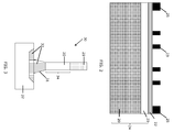
- the layer arranged for patterning the underlying layers may itself be patterned, e.g. via lithography, to form a nanometerscale temporary mask 23 that protects selected areas of the underlying layers 20, 21 during subsequent process steps. In the particular method illustrated, some of the selected areas protected by the mask 23 are the areas where later during the process nanowires will be formed. Other areas of the mask 23, indicated by features 25 in FIG. 2 , are provided to ensure proper flatness after CMP.
- the mask 23 is then used for processing the layers underneath the mask 23: the hard mask 22, the sacrificial layer 21 and the substrate 20.
- the hard mask 22 and the sacrificial layer 21 as well as part of the substrate 20 are removed by any suitable method from locations where no mask features 23 are present, for example by dry etching, thus forming at least one nanowire 30 on the remainder part of the substrate 20.
- the thus formed at least one nanowire 30 may have a sloped bottom profile 31, as illustrated in FIG. 3 . Such sloped bottom profile 31 may improve the stability of the nanowire 30.
- the diameter of the nanowire 30 may be between 1 and 500 nm, e.g. between 2 and 200 nm, and the length of the nanowire may be between 5 nm and 2 ⁇ m, e.g.
- a well 32 of a particular dopant type may be formed in the substrate 20.
- a well 32 of a first dopant type e.g. N-type well
- P-type second dopant type
- a well of a second dopant type e.g.
- P-type well may be provided in the substrate 20 where a nanowire 30 with a bottom junction 33 of a first type (N-type) is to be provided.
- Suitable masks and suitable dopant elements may be used for performing the well implantations, so that first one or more wells 32a of a first dopant type and thereafter one or more wells 32b of a second dopant type may be formed (or vice versa) ⁇ see also FIG. 4 .
- an anneal may take place for diffusing the dopant atoms into substitutional positions in the crystal lattice.
- a bottom junction implantation is performed (step 206) with a particular dopant type, for forming the bottom junction 33 of the nanowire 30.
- the dopant type is different from the dopant type of the well 32 in which the bottom junction 33 is formed.
- the dopant type used for the bottom junction 33 determines the device type (mode of operation).
- the dopant level of the bottom junction 33 is high, for example in the range of 10 18 /cc to 10 21 /cc. In particular embodiments, the doping level of the bottom junction 33 is in the range of 10 19 /cc to 5.10 20 /cc.
- Suitable masks and suitable dopant elements may be used for performing the bottom junction implantations. After the implantations have been performed, an anneal may take place for diffusing the dopant atoms into substitutional positions in the crystal lattice and under the nanowire.
- Both the well implantations and the bottom junction implantations may be performed under 0° tilt.
- the hard mask 22 and the sacrificial layer 21 protect the channel 34 formed by the substrate 20 material of the nanowire 30 during implantation.
- the implantations may be performed after the deposition of a protection layer, for example an oxide layer, on the channel 34 of the nanowire 30, to avoid implantation of species in the channel 34.
- a protection layer for example an oxide layer
- implantation may be performed in the presence of a post etch curing oxide.
- post etch curing oxide stops implantation of dopants into the channel 34, cures possible defects to get rid of etch damage and smoothes the sidewalls of the channel 34.
- the resulting structure is illustrated in FIG. 3 .
- the hard mask 22 is removed (step 207), for example by etching back or by resist stripping, e.g. in-situ removal takes place.
- a bottom insulating layer 40 is provided around the at least one nanowire 30, and between the nanowires 30 if a plurality of these have been provided. This way, the one or more nanowires 30 are embedded in the insulating layer 40.
- This insulating layer 40 insulates the nanowires 30 from one another.
- the bottom insulating layer 40 may comprise or consist of oxide, such as for example low-k oxide, HDP oxide or another suitable insulating material, for example conformally deposited insulating materials.
- the sloped bottom profile 31 of the nanowires 30a, 30b may be beneficial for trench filling, as it allows an easier filling of the space between the nanowires. Furthermore, the sloped bottom profile 31 of the nanowires 30a, 30b gives rise to good mechanical stability.
- the bottom insulating layer 40 is planarized, for example by CMP, stopping on the nanowires 30.
- the bottom insulating layer 40 may be planarized to a level above the nanowires 30, and further etched back down to the level of the top of the nanowires 30
- bottom insulating material 40 around the at least one nanowire and planarization thereof is illustrated in FIG.4 for a particular case of two nanowires 30a, 30b of different types, provided respectively above wells 32a, 32b of different types and having bottom junctions 33a, 33b of different types.
- FIG. 4 an embodiment is illustrated in which during previous steps a P-well 32a and an N-well 32b are provided.
- the formed bottom junctions are an N + -junction 33a at the bottom of the nanowire 30a on the P-well 32a, and a P + -junction 33b at the bottom of the nanowire 30b on the N-well 32b.
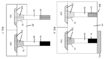
- this layer 40 may be opened (step 209) at the level of a first type of tunnel junction (in practice this may be at the level of one or more nanowires of a first type), in the embodiment illustrated at the level of the right hand nanowire 30a, provided above the N + -junction 33a in the P-well 32a.
- a protection material 50 for example a protection oxide
- resist patterning may be used, which may be based on a same reticle as the one for the bottom junction implantation for forming the bottom junction(s) 33a.
- the thus provided resist mask may be used for opening the insulating layer 40, as illustrated at the right hand side of FIG. 5 , at the level of one or more nanowires 30 of a particular type.
- the sacrificial layer 21 in the nanowire 30a which is revealed by opening the insulating layer 40 is removed by an appropriate selective removal mechanism, for example a selective etchback of the sacrificial layer material, e.g. ⁇ -SiGe, towards the material of the channel 34, e.g. i-Si, and the material of the insulating layer 40, e.g. oxide.
- the obtained hole is filed, e.g. by in-situ deposition, with suitable tunnel diode material 41 of a first type, e.g. P+ doped c-SiGe.
- the tunnel diode material 41 is Si 1-x Ge x with x>0.5.
- the steps of removal of the sacrificial layer 21 and provision of the tunnel diode material 41 can be performed in one step in an epireactor.
- the doping level of the tunnel diode material 41 is high, for example in the range of 10 18 /cc to 10 21 /cc. In particular embodiments of the present invention, the doping level may be in the range of 10 19 /cc to 5x10 20 /cc.
- the doping level of the tunnel diode material 41 may be higher than the doping level of the bottom junction 33a.
- a protection material 51 for example a protection oxide is provided, e.g. deposited, on this first tunnel junction 41.
- the insulating layer 40 is then opened at the level of a second type of tunnel junction, in the embodiment illustrated at the level of the left hand nanowire 30b, provided above the P + -junction 33b.
- resist patterning may be used, which may be based on a same reticle as the one for the bottom P + -junction implantation 33b.
- the thus provided resist mask may be used for opening the insulating layer 40, as illustrated at the left hand side of FIG. 6 , at the level of one or more nanowires 30 of a particular type.
- a next step 212 after opening the insulating layer 40, the sacrificial layer 21 in the nanowire 30b which is revealed by opening the insulating layer 40, is removed by an appropriate selective removal mechanism, for example a selective etchback of the sacrificial layer material, e.g. ⁇ -SiGe, towards the material of the channel 34, e.g. i-Si, and the insulating layer material 40, e.g. oxide.
- the obtained hole is filed, e.g. by in-situ deposition, with suitable tunnel diode material 52 of a second type, e.g. N+ doped c-III/V material, e.g.
- the steps of removal of the sacrificial layer 21 and provision of the tunnel diode material 52 can be performed in one step in an epireactor.
- the doping level of the tunnel diode material 52 is high, for example in the range of 10 18 /cc to 10 21 /cc. In particular embodiments of the present invention, the doping level may be in the range of 10 19 /cc to 5x10 20 /cc.
- the doping level of the tunnel diode material 52 may be higher than the doping level of the bottom junction 33b.
- first a first type of nanowires 30a can be opened and thereafter a second type of nanowires 30b. This way, different processing can be performed for different types of nanowires 30a, 30b. This is different from blanket type processing where no choice of different materials is possible.
- the bottom insulating layer 40 is partially removed (step 213), e.g. etched back. Such removal is selective towards the channel material 34, e.g. i-Si, and the P and N-type material 41, 52 of the top junction, e.g. c-SiGe and C-III/V material, respectively.
- the amount of insulating layer material 40 which is left after the partial removal forms the bottom insulation 60.
- the thickness of the bottom insulation 60 determines the intrinsic channel length outside the gate region which is needed to suppress the parasitic gate capacitance, to avoid gate leakage, to suppress the ambipolar behavior of the device, and to keep the intrinsic Si channel outside the gate region as short as possible for reduction of the sheet resistance.
- a thin crystalline shell 70 is grown (step 214) around the exposed nanowires, e.g. Si/SiGe nanowires, as illustrated in FIG. 8 .
- the shell 70 is provided on all free surfaces of the formed nanowires 30a, 30b and functions as a passivation layer for the heterojunction.
- the shell 70 can have a thickness of about 1 to 3 nm, preferably a thickness of only a few mono layers.
- the shell material depends on the channel and heterojunction materials, as the shell 70 has to be compatible with both.
- Si is a possible candidate material for the shell 70, in view of the channel being made from i-Si and the heterojunction being made from either c-SiGe or C-III/V material.
- An advantage of providing such shell 70 is that a regular and uniform layer may be grown on top thereof, over the junction.
- the shell 70 avoids surface dependent gate dielectric quality in the gate overlap region on the heterojunction.
- the shell 70 thickness may be optimized taking into account the consumption of the shell material during the next processing steps of the integration flow (the shell 70 has to withstand the next steps), and the electrical effect of its presence underneath the gate stack.
- a gate stack may be provided onto the sidewalls of the channel 34 of the nanowires 30a, 30b and patterned, as illustrated in FIG. 9 .
- Such gate stack may comprise a high-k dielectric layer 80, e.g. a high-k oxide such as hafnium oxide, which is provided on the shell 70 and optionally partly also on the bottom insulation 60.
- the thickness of the high-k dielectric layer 80 may be in the range of 0.5 nm to 20 nm.
- the gate dielectric 80 covers the outer walls of the channel 34.
- a metal gate 81 is provided on top of the high-k dielectric layer 80. This metal gate 81 determines the workfunction of the TFET.
- Suitable metals for forming the metal gate 81 may be Al, W, Ta, Ti, Ru, Pd, Rh, Re, Pt and alloys thereof.
- a layer of a suitable material for later on forming a low resistive metal contact is provided, e.g. an amorphous semiconductor layer, for example an ⁇ -Si layer 82, as used in CMOS for electrically contacting the metal gate 81.
- the thickness of the ⁇ -Si layer 82 is optimized for a pre-determined silicide thickness to be obtained later during the process.
- the complete gate stack, i.e. the high-k dielectric layer 80, the metal gate 81 and the ⁇ -Si layer 82 have a thickness such that the total stack thickness determines the minimum gate length.
- the gate stack 80, 81, 82 may optionally be patterned (step 216) for separating the different gate stacks from one another (not illustrated in the drawings).
- This patterning may be performed by means of a resist masked dry etch of the gate stack 80, 81, 82 in an isotropic way.
- the patterning is such that gate stacks of nanowires of different type are not electrically connected to each other.
- This patterning is such that the metal gate 81 does not extend over the dielectric layer 80, hence is not in direct contact with any of the shell 70 or the bottom insulation 60.
- the gate structure comprising gate dielectric 80 and metal gate 81 can be referred to as an all around gate structure.
- Patterning of the gate stack for separation of the gates does not need to be performed immediately after the gate stack deposition; it can also be done later. However, patterning the gate stack immediately after deposition thereof avoids problems near the dummy structures for CMP.
- a gate hard mask 90 is provided over the gate stack.
- This gate hard mask 90 may for example be an oxide layer, e.g. a HDP oxide.
- the material of the gate hard mask may be different from the material of the bottom insulation layer 60.
- the provided gate hard mask 90 is planarised, for example by a mechanical planarization method such as e.g. CMP, followed by an etch back step for removing part of the gate hard mask material around the nanowires, so as to reveal the top of the nanowires as illustrated in FIG. 9 .
- the thickness T HM of the remaining hard mask 90 must be sufficient to guarantee that the gate stack 80, 81, 82 after patterning using the hard mask 90 overlaps on the tunnel junction formed between the channel 34 and the tunnel diode material 41, 52.
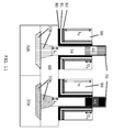
- the gate hard mask 90 is furthermore patterned so as to reveal parts of the gate stack 80, 81, 82 where gates of different nanowires need to be separated. This is illustrated in FIG. 10 .
- the gate hard mask 90 is used in a next step 218 as a hard mask to pattern the gate stack 80, 81, 82. This is illustrated in FIG. 11 .
- the patterning of the gate stack 80, 81, 82 comprises subsequent removal steps of the revealed part of a-Si layer 82, of the revealed part of the metal layer 81 and of the revealed part of the high-k dielectric layer 80.
- By patterning the gate stack 80, 81, 82 part of the shell 70 is revealed. If the shell 70 is a Si shell, standard CMOS recipes can be used during further processing.
- the gate length Lg is defined, which corresponds to the thickness T HM of the hard mask 90.
- the thickness T HM of the hard mask 90 defines the gate overlap Og, i.e. the length the gate overlaps the tunnel diode material 41, 52.
- the length of the gate overlap O g determines the amount of tunneling.
- the sloped bottom profile 31 of the nanowire 30 reduces the series resistance and the length Lc of the channel 34 between the gate stack 80, 81, 82 and bottom junctions 33a, 33b while maintaining sufficient distance between the gate stack 80, 81, 82 and the bottom junctions 33a, 33b in the substrate 20 or well 32, thus reducing the parasitic gate capacitance to the bottom junction 33.
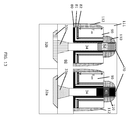
- the revealed part of the nanowires is insulated (step 219). This may optionally be done by first providing insulation spacers 110 against the sidewalls of the revealed parts of the nanowires, as illustrated in FIG. 12 . Further insulating spacers 112 may also be formed at the sidewalls of the gate hard mask 90.
- the spacers 110, 112 may for example be formed by blanket deposition of an insulation layer material, for example SiN, and removing a portion of the insulation layer material so that spacers 110 are formed on the sidewalls of the revealed part of the nanowire and spacers 112 are formed on the sidewalls of the gate hard mask 90.
- Removing a portion of the insulation layer material may be done by etching the insulation layer material.
- the insulating spacers 110 are not strictly necessary for insulating the revealed part of the nanowires. Top isolation without spacers 110 is possible in accordance with embodiments of the present invention. Nevertheless, the optional spacers 110 are advantageous for avoiding cross contamination of the metal gate. Furthermore, the insulation spacers 110 may also be used as a stressor layer for strain engineering. Strain engineering leads to bandgap variation, which may provide tunneling efficiency tuning.
- a further insulation layer 111 may be provided over the gate hard mask 90, the insulation spacers 110, 112 and the revealed parts of the nanowires.
- the further insulation layer 111 may be deposited. It may comprise or consist of for example HDP oxide. Once provided, e.g. deposited, the further insulation layer 111 may be planarized, for example in a mechanical planarization step such as CMP, and an insulating material etch back may be performed so as to reveal the top of the nanowires (step 220). This is illustrated in FIG. 13 .
- the further insulation material 111 may be different from the gate hard mask material 90, but should be compatible with etching and cleaning chemistry used during future opening of contact regions.
- the thickness of the insulation is determined by the insulating properties to be obtained, and should be sufficient to suppress leakage between source and drain, and to suppress a capacitance formed between gate and source.
- Tunnel diode routing material 130 may be applied (step 222), as illustrated in FIG. 15 , for electrically contacting to the tunnel diode material 41, 52 of the nanowires.
- the tunnel diode routing material 130 may be conductive material such as for example highly doped ⁇ -Si material, e.g. with a doping level in the range of 10 18 /cc to 10 21 /cc, which may for example be deposited.
- the diode routing material 130 may have an optimized thickness so that it can be silicided, optionally fully silicided, later on.
- a pre-treatment may be performed to ensure a good contact between the routing material 130 and the nanowire.
- the pre-treatment may for example be a HF-based pre-treatment.
- the tunnel diode routing material 130 may be patterned in a conventional way, e.g. by a resist based patterning step.
- the patterned tunnel diode routing material 130 provides a routing for electrically contacting the nanowires.
- the gate, junction and substrate contacts are opened (step 223). This is illustrated in FIG. 16 .
- a resist layer may be applied on top of the structure of FIG. 15 .
- This resist layer may be patterned so that it covers and protects the tunnel diode routing material 130, but provides the possibility to create openings towards the contact regions of the bottom junctions, the substrate and the gate. Only openings 140 towards the gate and partially towards a substrate contact region is demonstrated in the process scheme illustrated. Common gate/substrate or gate/junction openings do not form a problem since the bottom isolation will separate them.
- the resist layer (not illustrated in FIG. 16 ) is then used for creating the openings 140, for example by etching.
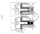
- the sidewalls of the openings 140 may be protected by forming protective spacers 141 on these sidewalls, as illustrated in FIG. 17 .
- This may be performed for example by deposition of protective material layer, for example SiN, and removing a portion of the protective material layer so that the spacers 141 are formed on the sidewalls of the formed openings 140. Removing a portion of the protective material layer may be done by etching the protective material layer.
- a thin conformal layer may be deposited of which the thickness is taken into account during a soft sputter etch. This latter solution is less complex than providing spacers.
- a silicidation step (step 224) is carried out for silicidation of the silicon material at the contact regions.
- the silicidation step may be performed by providing metal onto the revealed silicon contact regions and making both react with one another in a conventional way.
- FIG. 17 illustrates the device after silicide formation on the contact regions.
- the openings 140 may be refilled with filler material (not illustrated in FIG. 17 ), for example with an oxide or a conventional BEOL stack.
- the oxide may be deposited.
- the filler material may be planarized so as to obtain a planar structure.
- a method according to a second embodiment of the present invention is schematically illustrated in a flowchart shown in FIG. 18 and is described in detail below. It has, however, to be understood that this is only an example of a suitable method for forming a device according to the invention, and that the sequence of the process steps as described hereinafter is not limiting the invention.
- a number of steps of this method according to the second embodiment of the invention are as in the method according to the first embodiment of the invention, and are therefore not disclosed here in as much detail as above. Details which are lacking in the description of the second embodiment can be taken from the description of the first embodiment.
- a major difference between a method according to the first embodiment and a method according to the second embodiment is that in the first embodiment the heterojunction is formed at the beginning of the manufacturing method, while in the second embodiment the heterojunction is formed at the end of the manufacturing method.
- a substrate 20 is provided.
- said substrate 20 is a semiconductor substrate, e.g. a silicon substrate or a silicon on insulator (SOl) substrate.
- the semiconductor substrate 20 may be intrinsic to lowly doped with a particular dopant type, e.g. P-type doped, and with a doping level which may be in the range of intrinsic to 10 16 /cc doping.
- the semiconductor substrate 20 may have any suitable thickness for providing the nanowire channel and bottom junction region for the NW-TFET structure to be provided on the substrate 20, for example between 20 nm and 750 ⁇ m.
- a sacrificial layer 21 is provided (step 251).
- the sacrificial layer can be made of any suitable crystalline material which is selectively removable towards the underlying substrate 20, and towards a hardmask 22 to be provided on top thereof.
- the sacrificial layer 21 can for example comprise or consist of crystalline semiconductor material, for example crystalline SiGe. SiGe may be particularly good as a semiconductor material to be applied on a silicon substrate 20, in view of its being able to be manufactured on silicon wafers using conventional silicon processing toolsets.
- the sacrificial layer 21 may have a thickness which is at least sufficient to isolate the source contact from the gate and still have a gate overlap, for example a thickness of about 120 nm.
- the substrate 20 and the sacrificial layer 21 together form a stack 24.
- a hardmask layer 22 is provided (step 252) on the sacrificial layer 21.
- the hardmask layer 22 may for example consist of a material suitable for being used during lithography (patterning), such as for example a low temperature oxide or nitride.
- the hardmask layer 22 is provided for later on patterning the underlying substrate 20 and sacrificial layer 21.
- the hardmask 22 may have a thickness in the range of 1 nm up to 100 nm, for example in the range of 2 nm up to 10 nm.
- the hardmask layer 22, the sacrificial layer 21 and the substrate 20 are patterned. This may be obtained by, on the hard mask 22, providing a layer arranged for patterning the underlying layers forming a nanometerscale temporary mask 23 that protects selected areas of the underlying layers 20, 21 during subsequent process steps. In the particular method illustrated, some of the selected areas protected by the mask 23 are the areas where later during the process nanowires will be formed.
- the mask 23 is then used for processing the layers underneath the mask 23: the hard mask 22, the sacrificial layer 21 and the substrate 20.
- the hard mask 22 and the sacrificial layer 21 as well as part of the substrate 20 are removed by any suitable method from locations where no mask features 23 are present, for example by dry etching, thus forming at least one nanowire 30 on the remainder part of the substrate 20, as illustrated in FIG. 3 .
- the diameter of the nanowire 30 may be between 1 and 500 nm, e.g. between 2 and 200 nm, and the length of the nanowire may be between 5 nm and 2 ⁇ m, e.g. between 10 nm and 1 ⁇ m, depending on the thicknesses of the material layers and the depth of the etch in the substrate 20.
- well implantations may be performed underneath the at least one nanowire 30, so as to form in the substrate 20 a well 32 of a particular dopant type. Different types of wells 32 may be formed in the substrate 20. Suitable masks and suitable dopant elements may be used for performing the well implantations, so that first one or more wells 32a of a first dopant type and thereafter one or more wells 32b of a second dopant type may be formed (or vice versa) ⁇ see also FIG. 4 . After the well implantations have been performed, an anneal may take place for diffusing the dopant atoms into substitutional positions in the crystal lattice.
- a bottom junction implantation is performed (step 255) with a particular dopant type, for forming the bottom junction 33 of the nanowire 30.
- the dopant type is different from the dopant type of the well 32 in which the bottom junction 33 is formed.
- the dopant level of the bottom junction 33 is high, for example in the range of 10 18 /cc to 10 21 /cc, e.g. in the range of 10 19 /cc to 5.10 20 /cc.
- Suitable masks and suitable dopant elements may be used for performing the bottom junction implantations. After the implantations have been performed, an anneal may take place for diffusing the dopant atoms into substitutional positions in the crystal lattice.
- Both the well implantations and the bottom junction implantations may be performed under 0° tilt.
- the hard mask 22 and the sacrificial layer 21 protect the channel 34 formed by the substrate 20 material of the nanowire 30 during implantation.
- the implantations may be performed after the deposition of a protection layer, for example an oxide layer, on the channel 34 of the nanowire 30, to avoid implantation of species in the channel 34.
- a protection layer for example an oxide layer
- implantation may be performed in the presence of a post etch curing oxide. The resulting structure is illustrated in FIG. 3 .
- the hard mask 22 is removed (step 256), for example by etching back or by resist stripping, e.g. in-situ removal takes place.
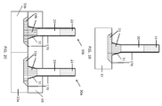
- the nanowire 30 is capped with a capping layer 170, as illustrated in FIG. 19 .
- the capping layer 170 is provided on all free surfaces of the nanowire 30.
- the capping layer material depends on the channel and heterojunction materials, as the capping layer 170 has to be compatible with both.
- Si is a possible candidate material for the capping layer 70, in view of the channel being made from i-Si and the sacrificial layer being made from crystalline material, e.g. c-SiGe.
- the capping layer 170 may be epitaxially grown. The thickness of the capping layer 170 may be in the range of 1 to 3 nm.
- the thickness of the capping layer 170 may be not more than a few atomic layers. This provision of the capping layer 170 is the reason why, in accordance with the second embodiment, the sacrificial material 21 needs to be crystalline material; otherwise a crystalline capping layer 170 cannot be grown onto it.
- the capping layer 170 thickness can be optimized taking into account the consumption of this capping layer 170 material during the next processing steps of the integration flow, and the electrical effect of its presence underneath the gate stack to be formed later.
- the capping layer 170 avoids surface dependent gate dielectric quality in the gate overlap region on the heterojunction.
- the capping layer 170 after provision of the bottom junction as in accordance with the second embodiment of the present invention is only possible in circumstances where the gate does not need to be contacted during opening of the contact areas. This means that in this case low resistive gate material is to be used with the desired work function. If not, the capping layer 170 blocks the etching during opening of the contact areas, as such etching needs to be selective towards the Si of the gate stack. Also during gate stack etching this capping layer cannot be removed because otherwise also the protection of the tunnel diodes would be etched away.
- a bottom insulation 60 is provided around the bottom part of the at least one nanowire 30, and between the nanowires 30 if a plurality of these have been provided, as illustrated in FIG. 20 .
- This insulating layer 60 insulates the nanowires 30 from one another.
- the bottom insulation 60 may comprise oxide, such as for example low-k oxide, HDP oxide or another suitable insulating material.
- a gate stack may be provided onto the sidewalls of the channel 34 of the nanowire 30 and patterned, as illustrated in FIG. 19 .
- Such gate stack comprises a high-k dielectric layer 80, e.g. a high-k oxide such as hafnium oxide, which is provided on the capping layer 170 and optionally partly also on the bottom insulation 60.
- the thickness of the high-k dielectric layer 80 may be in the range of 0.5 nm to 20 nm.
- the gate dielectric 80 covers the outer walls of the channel 34.
- a metal gate 81 is provided on top of the high-k dielectric layer 80. This metal gate 81 determines the workfunction of the TFET.
- Suitable metals for forming the metal gate 81 may be Al, W, Ta, Ti, Ru, Pd, Rh, Re, Pt and alloys thereof.
- a layer of a suitable material for later on forming a low resistive metal contact is provided, e.g. an amorphous semiconductor layer 82, e.g. ⁇ -Si, is provided, as used in CMOS for electrically contacting the metal gate 81.
- the thickness of the ⁇ -Si layer 82 is optimized for a pre-determined silicide thickness to be obtained later during the process.
- the complete gate stack, i.e. the high-k dielectric layer 80, the metal gate 81 and the ⁇ -Si layer 82 have a thickness such that the total stack thickness determines the minimum gate length.
- step 260 After providing the gate stack 80, 81, 82, it may optionally be patterned (step 260) for separating the different gate stacks from one another (not illustrated in the drawings).
- This patterning may be performed by means of a resist masked dry etch of the gate stack 80, 81, 82 in an isotropic way.
- the patterning is such that gate stacks of nanowires of different type are not electrically connected to each other.
- This patterning is such that the metal gate 81 does not extend over the dielectric layer 81, hence is not in direct contact with any of the shell 70 or the bottom insulation 60.
- the gate structure comprising gate dielectric 80 and metal gate 81 can be referred to as an all around gate structure.
- Patterning of the gate stack for separation of the gates does not need to be performed immediately after the gate stack deposition; it can also be done later. However, patterning the gate stack immediately after deposition thereof avoids problems near the dummy structures for CMP .
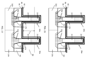
- a gate hard mask 90 is provided over the gate stack, as illustrated in FIG. 22 .
- This gate hard mask 90 may for example be an oxide layer, e.g. a HDP oxide.
- the material of the gate hard mask may be different from the material of the bottom insulation layer 60.
- the provided gate hard mask 90 is planarised, for example by a mechanical planarization method such as e.g. CMP, followed by an etch back step for removing part of the gate hard mask material around the nanowires, so as to reveal the top of the nanowires as illustrated in FIG. 22 .
- the thickness T HM of the remaining hard mask 90 must be sufficient to guarantee that the gate stack 80, 81, 82 after patterning using the hard mask 90 overlaps on the tunnel junction formed between the channel 34 and the tunnel diode material which will replace the sacrificial material 21.
- the gate hard mask 90 is furthermore patterned so as to reveal parts of the gate stack 80, 81, 82 where gates of different nanowires need to be separated. This is illustrated in FIG. 23 .
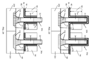
- the gate hard mask 90 is used in a next step 262 as a hard mask to pattern the gate stack 80, 81, 82. This is illustrated in FIG. 24 .
- the patterning of the gate stack 80, 81, 82 comprises subsequent removal steps of the revealed part of ⁇ -Si layer 82, of the revealed part of the metal layer 81 and of the revealed part of the high-k dielectric layer 80.
- By patterning the gate stack 80, 81, 82 part of the capping layer 170 is revealed. If the capping layer 170 is made from Si, standard CMOS recipes can be used during further processing.
- the gate length Lg is defined, which corresponds to the thickness T HM of the hard mask 90.
- the thickness T HM of the hard mask 90 defines the gate overlap Og, i.e. the length the gate overlaps the sacrificial layer 21, which later on will be replaced by tunnel diode material.
- the revealed part of the nanowire 30 is insulated (step 263). This may be done by first providing insulation spacers 110 against the sidewalls of the revealed parts of the nanowires . Further insulating spacers 112 may also be formed at the sidewalls of the gate hard mask 90.
- the spacers 110, 112 may for example be formed by blanket deposition of an insulation layer material, for example SiN, and removing a portion of the insulation layer material so that spacers 110 are formed on the sidewalls of the revealed part of the nanowire 30 and spacers 112 are formed on the sidewalls of the gate hard mask 90.
- Removing a portion of the insulation layer material may be done by etching the insulation layer material.
- the insulating spacers 110 are not strictly necessary for insulating the revealed part of the nanowires. Top isolation without spacers 110 is possible in accordance with embodiments of the present invention. Nevertheless, the optional spacers 110 are advantageous for avoiding cross contamination of the metal gate. Furthermore, the insulation spacers 110 may also be used as a stressor layer for strain engineering. Strain engineering leads to bandgap variation, which may provide tunneling efficiency tuning.
- a further insulation layer 111 may be provided over the gate hard mask 90 (step 262), the insulation spacers 110 and the revealed parts of the nanowires 30.
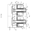
- the further insulation layer 111 may be deposited. It may comprise or consist of for example HDP oxide. Once provided, e.g. deposited, the further insulation layer 111 may be planarized, for example in a mechanical planarization step such as CMP, and an insulating material etch back may be performed so as to reveal the top of the nanowires 30 (step 264). This is illustrated in FIG. 25 .
- the further insulation material 111 may be different from the gate hard mask material 90, but should be compatible with etching and cleaning chemistry used during future opening of contact regions.
- the capping layer 170 is removed, e.g. etched back, from the top of the nanowires 30 (step 265), so as to reveal the sacrificial material 21 of the nanowires 30 ⁇ see FIG. 26 .
- This etching back of the capping layer 170 may be performed selectively for one type of nanowire 30 at a time; in FIG. 26 it is illustrated for the right hand nanowire 30a.
- resist patterning may be used, which may be based on a same reticle as the one for the bottom junction implantation for forming the bottom junction(s) 33a.
- the thus provided resist mask (not illustrated in the drawings), may be used for etching back the capping layer 170 at the level of one or more nanowires 30 of a particular type, while nanowires 30 of another type remain covered by the capping layer 170.
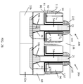
- the sacrificial layer 21 in the nanowire 30a which is revealed by etching back the capping layer 170 of that nanowire 30b, is removed (step 266) by an appropriate selective removal mechanism, for example a selective etchback of the sacrificial layer material 21, e.g. c-SiGe, towards the material of the channel 34, and the material of the capping layer 170.
- the obtained hole is filed, e.g. by in-situ deposition, with suitable tunnel diode material 41, e.g. P+ doped c-SiGe.
- the tunnel diode material 41 is Si 1-x Ge x with x>0.5.
- the steps of removal of the sacrificial layer 21 and provision of the tunnel diode material 41 can be performed in one step in an epireactor.
- the doping level of the tunnel diode material 41 is high, for example in the range of 10 18 /cc to 10 21 /cc. In particular embodiments of the present invention, the doping level may be in the range of 10 19 /cc to 5x10 20 /cc.
- the doping level of the tunnel diode material 41 may be higher than the doping level of the bottom junction 33a.
- a protection material for example a protection oxide may be provided, e.g. deposited, on this first tunnel junction 41 (not illustrated in the drawings).
- the capping layer 170 is then etched back at the level of a second type of tunnel junction, in the embodiment illustrated at the level of the left hand nanowire 30b.
- resist patterning may be used, which may be based on a same reticle as the one for the bottom P + -junction implantation 33b.
- the thus provided resist mask (not illustrated in the drawings), may be used for etching back the capping layer 170 at the level of one or more nanowires 30b of a second type.
- the sacrificial layer 21 in the nanowire 30b which is revealed by etching back the capping layer 170 is removed by an appropriate selective removal mechanism, for example a selective etchback of the sacrificial layer material 21, e.g. c-SiGe, towards the material of the channel 34, e.g. i-Si, and the material of the capping layer 170.
- the obtained hole is filed, e.g. by in-situ deposition, with suitable tunnel diode material 52 (step 267), e.g. N+ doped c-III/V material, e.g.
- the steps of removal of the sacrificial layer 21 and provision of the tunnel diode material 52 can be performed in one step in an epireactor.
- the doping level of the tunnel diode material 51 is high, for example in the range of 10 18 /cc to 10 21 /cc. In particular embodiments of the present invention, the doping level may be in the range of 10 19 /cc to 5x10 20 /cc.
- the doping level of the tunnel diode material 52 may be higher than the doping level of the bottom junction 33b.
- first a first type of nanowires 30a can be opened and thereafter a second type of nanowires 30b. This way, different processing can be performed for different types of nanowires 30a, 30b, although present on a same substrate area.
- the remainder of the processing is as described with respect to the first embodiment, and is not repeated here again. It may comprise some or all of the steps of providing and patterning tunnel diode routing material (step 268), opening the gate, junction and substrate contacts (step 269), providing protection to the sidewalls of the openings, silicidizing the revealed gate, junction and substrate contacts (step 270), and refilling the openings with filler material. Further processing of the semiconductor device thus obtained may be conform with the standard back end of line CMOS processing.
- defects may appear at the interface between the channel 34 and the heterojunction 41, 52 due to lattice mismatch, depending on the thickness of the heterojunction layer 41, 52 to be provided and diameter ⁇ NW of the nanowire 30a, 30b.
- This problem can be alleviated by growing a thin crystalline heterojunction, possibly a crystalline heterojunction comprising a plurality of crystalline layers 230, 231 as illustrated in FIG. 28 , and continuing the growth of the heterojunction with an amorphous layer 232.
- the crystalline layers 230, 231 may for example be a c-Ge and a c-SiGe layer. This avoids facet limited growth in small windows.
- a defect-free channel/heterojunction interface may be obtained by limiting the crystalline layer thickness with a maximum Ge content and doping concentration. Tunneling is not affected for a maximum bandgap lowering with an as abrupt as possible junction profile.
- a few atomic layers e.g. not more than 20 atomic layers, such as not more than 10 atomic layers or not more than 5 atomic layers, of pure Ge or SiGe (with an as high as possible Ge content) may be provided at the interface of the P-type tunnel junction with the channel 34 to avoid P-type dopant diffusion, e.g. B-diffusion, in the channel 34. This improves the junction abruptness.
- layers 231 and 232 may be B-doped layers.
- layers 231 and 232 may be B-doped layers.
- an n+ Si layer 233 may be provided under the diffusion barrier layer 230, e.g. a c-Ge layer.
- a limitation on the thermal budget is the consequence.
- n+ source e.g. III-V material
- a p+ layer is a good option for layer 233 an n+ region may be provided between a p+ tunnel diode 232 and an i-Si channel 34.
Landscapes
- Engineering & Computer Science (AREA)
- Chemical & Material Sciences (AREA)
- Nanotechnology (AREA)
- Physics & Mathematics (AREA)
- Mathematical Physics (AREA)
- Theoretical Computer Science (AREA)
- Crystallography & Structural Chemistry (AREA)
- Metal-Oxide And Bipolar Metal-Oxide Semiconductor Integrated Circuits (AREA)
- Thin Film Transistor (AREA)
Abstract
Description
- The present invention relates to the field of semiconductor devices and nanotechnology. More specifically, the invention relates to a nanostructure semiconductor device, more specifically a tunnel field effect transistor having a heterostructure nanowire, and a method for manufacturing such tunnel field effect transistor devices with integrated nanowires. In particular the present invention relates to a method for manufacturing complementary vertical TFETS, and to complementary TFETs thus obtained.
- Microelectronic devices are generally fabricated on semiconductor substrates as integrated circuits. A complementary metal-oxide-semiconductor (CMOS) field effect transistor is one of the core elements of the integrated circuits. Dimensions and operating voltages of CMOS transistors are continuously reduced, or scaled down, to obtain ever-higher performance and packaging density of the integrated circuits.
- One of the problems due to the scaling down of CMOS transistors, is that the power consumption keeps increasing. This is partly because leakage currents are increasing (e.g. due to short channel effects) and because it becomes difficult to decrease the supply voltage. The latter is mainly due to the fact that the subthreshold slope is limited to minimally about 60 mV/decade, such that switching the transistor from ON to OFF needs a certain voltage variation and therefore a minimum supply voltage.
- Tunnel field-effect transistors (TFETs) are typically advertised as successors of metal-oxide semiconductor field-effect transistors (MOSFETs), because of their absence of short-channel effects and because of their resulting low off-currents. Another advantage of TFETs is that the subthreshold slope can be less than 60 mV/dec, the physical limit of conventional MOSFETs, such that potentially lower supply voltages can be used. However, TFETs typically suffer from low on-currents, a drawback related to the large resistance of the tunnel barrier.
- Silicon-based TFETs are the most attractive because they allow for a full re-use of the existing expertise in fabricating high-quality silicon-compatible gate dielectrics. However, the small band-to-band tunneling efficiency in large-bandgap silicon results in low on-currents of the all-silicon TFETs. To improve the on-currents while maintaining a silicon-channel, the incorporation of heterostructures has been proposed.
- In
EP1900681 , a method of fabricating an improved TFET using nanowires is disclosed. The method comprises providing a source contact on a substrate, and growing on the source contact a nanowire structure having an integrated source region, a channel region, a heterosection, and a drain region. The source region, channel region and drain region are made from a first semiconductor material and the heterosection is made from a second material with a lattice constant which is different from the lattice constant of the first semiconductor material. The method further comprises selectively doping the source region, the channel region, the heterosection and the drain region to a desired doping level and dopant type, depositing on sidewalls of the nanowire structure a gate dielectric and a gate electrode, and forming a drain contact on top of the drain region of the nanowire. - Different TFET integration approaches exist. They can be classified on the one hand in top-down approaches, and on the other hand in bottom-up approaches. For the known top-down approaches, the bottom junction, the instrinsic doped Si and the top diode (in situ doped Si or heterostructures) are epitaxially grown before the nanowire patterning. Complementary devices need to have an epitaxial growth in two steps: one with P-top and one with N-top. An issue with known catalyst based bottom-up approaches is metal contamination. Therefore the nanowires can be selectively grown in an oxide template (growth in holes). This means selective growth of the intrinsic Si channel in situ, followed by the growth of the heterojunction which makes the integration scheme complex for complementary devices.
- It is an object of embodiments of the present invention to provide good method for manufacturing semiconductor device structures using elongate nanostructures as nanowires.
- The above objective is accomplished by a method according to the present invention. Corresponding devices are also provided.
- In a first aspect, the present invention provides a method for manufacturing at least one nanowire Tunnel Field Effect Transistor (TFET) semiconductor device. The method comprises providing a stack comprising a layer of channel material with on top thereof a layer of sacrificial material, removing material from the stack so as to form at least one nanowire from the layer of channel material and the layer of sacrificial material, and replacing the sacrificial material in the at least one nanowire by heterojunction material.
- The presence of heterojunction material in the at least one nanowire increases tunneling in the TFET device. A method according to embodiments of the present invention is advantageous as replacing the sacrificial material by heterojunction material as proposed makes the manufacturing process of the nanowire TFET semiconductor device independent from the dopant type of the nanowire.
- Furthermore, in embodiments of the present invention only small amounts of heterojunction material are grown, thinner than the mismatch, hence the devices obtained exhibit less mismatch compared to prior art devices.
- In a method according to embodiments of the present invention, providing a stack comprises providing a layer of crystalline channel material. Such crystalline material allows growing a capping layer later on.
- A method according to embodiments of the present invention may furthermore comprise, after forming the at least one nanowire, embedding the at least one nanowire in insulating material.
- A method according to embodiments of the present invention may furthermore comprise, before embedding the at least one nanowire in insulating material, covering the at least one nanowire with a capping layer. Such capping layer may provide a basis for forming a regular and uniform layer on top during further processing of the TFET device.
- Covering the at least one nanowire with a capping layer may comprise providing a few atomic layers of semiconductor material, such as for example silicon.
- In a method according to embodiments of the present invention, replacing the sacrificial material in the at least one nanowire by heterojunction material may comprise selectively etching back the sacrificial material. This is an easy and well-known process.
- A method according to embodiments of the present invention, furthermore comprising forming a gate stack around the nanowire. This way, an all around gate may be formed.
- In a method according to embodiments of the present invention, replacing the sacrificial material in the nanowire by heterojunction material may be performed before formation of the gate stack. This has the advantage that no gate dielectric is present at that moment in time yet, and that hence gate dielectric material is not degraded by the process of replacing the sacrificial material by heterojunction material.
- In alternative embodiments, however, replacing the sacrificial material in the nanowire by heterojunction material may be performed after formation of the gate stack. In this case, the final heterojunction is not subject to as much thermal budget as in the case of provision of heterojunction first; hence less diffusion of dopants out of the heterojunction takes place.
- A method according to embodiments of the present invention may be arranged for manufacturing at least one nanowire Tunnel Field Effect Transistor semiconductor device of a first dopant type and at least one nanowire Tunnel Field Effect Transistor semiconductor device of a second dopant type. In such case, replacing the sacrificial material in a nanowire by heterojunction material may first be performed for at least one nanowire of the first dopant type and thereafter for at least one nanowire of the second dopant type. The method according to such embodiments of the present invention allows for providing complementary NW-TFETs.
- In a second aspect, the present invention provides a semiconductor device as obtained by method embodiments according to the first aspect of the present invention.
- In a third aspect, the present invention provides a semiconductor device comprising at least one vertical TFET comprising a nanowire comprising channel material and a heterojunction. The nanowire is surrounded by a shell underneath the gate stack, at least at the interface between the channel material and the heterojunction. The shell may for example be a crystalline shell. The shell may for example be a silicon shell.
- In a semiconductor device according to embodiments of the present invention, at least two vertical TFETs may be provided, at least two of the at least two vertical TFETs being of different types. A first type may be an N-type of TFET and a second type may be a P-type of TFET. Such device is a complementary device.
- It is an advantage of a method for manufacturing a NW-TFET according to embodiments of the present invention that Si based materials and process knowledge can be used to create the NW-TFET such that the NW-TFET manufacturing can be easily processed an incorporated in current Si-based technology devices.
- A manufacturing method according to embodiments of the present invention is distinguished from prior art manufacturing methods in that it allows processing of different dopant types of NW-TFETs (complementary TFETs) on a same substrate area.
- Particular and preferred aspects of the invention are set out in the accompanying independent and dependent claims. Features from the dependent claims may be combined with features of the independent claims and with features of other dependent claims as appropriate and not merely as explicitly set out in the claims.
- For purposes of summarizing the invention and the advantages achieved over the prior art, certain objects and advantages of the invention have been described herein above. Of course, it is to be understood that not necessarily all such objects or advantages may be achieved in accordance with any particular embodiment of the invention. Thus, for example, those skilled in the art will recognize that the invention may be embodied or carried out in a manner that achieves or optimizes one advantage or group of advantages as taught herein without necessarily achieving other objects or advantages as may be taught or suggested herein.
-
-
FIG. 1 is a flow chart of a method for manufacturing complementary vertical TFETs according to a first embodiment of the present invention. -
FIG. 2 to FIG.17 illustrate subsequent process steps in a manufacturing method according to the first embodiment of the present invention. -
FIG. 18 is a flow chart of a method for manufacturing complementary vertical TFETs according to a second embodiment of the present invention. -
FIG. 19 to FIG. 27 illustrate subsequent process steps in a manufacturing method according to the second embodiment of the present invention. -
FIG.28 illustrates an alternative embodiment for the heterojunction, which may be implemented both in a method according to the first and to the second embodiment. - The drawings are only schematic and are non-limiting. In the drawings, the size of some of the elements may be exaggerated and not drawn on scale for illustrative purposes.
- In the different drawings, the same reference signs refer to the same or analogous elements. Any reference signs in the claims shall not be construed as limiting the scope.
- The present invention discloses a method for manufacturing at least one nanowire Tunnel Field Effect Transistor semiconductor device. A method according to embodiments of the present invention comprises providing a stack comprising a layer of channel material with on top thereof a layer of sacrificial material, removing material from the stack so as to form a nanowire from the layer of channel material and the layer of sacrificial material, and replacing the sacrificial material in the nanowire by heterojunction material. Heterojunction material is semiconductor material which is different from other semiconductor material in the nanowire.
- A method according to embodiments of the present invention thus comprises introduction of a sacrificial layer, and later on replacing this sacrificial layer by heterojunction material.
- According to one embodiment of the method, complementary TFETs are manufactured, i.e. TFETs having nanowires having different dopant types. In a method according to this embodiment, the sacrificial layer is replaced after a bottom isolation layer is polished and the sacrificial layer is exposed (after CMP or after wet etchback). Next the sacrificial layer can be replaced by the heterojunctions in two steps (one step for each dopant type of nanowires):
- Opening and etchback of the dummy P-tunnel diode and growth of the P-tunnel diode
- Opening and etchback of the dummy N-tunnel diode and growth of the N-tunnel diode
- According to another embodiment of the method, the TFET semiconductor devices comprising nanowires with a sacrificial layer are processed until the top isolation is defined. Next the sacrificial layer is replaced by the heterojunctions as mentioned before.
- Advantages of methods according to embodiments of the present invention are that nanowire patterning for different dopant types of nanowire TFETs, e.g. N-TFET and P-TFET, is the same. The nanowire height is controlled, so that a same stack may be obtained for both devices. As long as the diameter ΦNW of the nanowires is small enough, the bottom junction can be defined by masked implants and diffusion steps.
- Methods according to embodiments of the present invention provide a better control of the gate overlap (as much overlap as possible is best) on the tunnel junction. The channel length is controlled. A facet-free channel material may be provided to start from.
- Methods according to embodiments of the present invention provide epitaxial growth on a damage free wafer surface, e.g. Si surface. Methods according to embodiments of the present invention provide less relaxation. Less problems with defects occur at the junction/channel interface due to the small exposed growth surface. The smaller the diameter of the nanowires, the less problems occur with lattice mismatch. There is a possibility to start with a crystalline hetero junction and to continue the growth with an amorphous layer to reduce the growth rate dependence on window sizes.
- Whenever reference is made hereinafter to a particular dopant type, this is done for the ease of explanation only and is not intended to limit the invention. It is to be understood that in the examples given herein below, materials and dopant types may be replaced by other suitable materials and dopant types, without changing the invention.
- The invention will now be described by a detailed description of several embodiments of the invention. It is clear that other embodiments of the invention can be configured according to the knowledge of persons skilled in the art without departing from the true spirit or technical teaching of the invention, the invention being limited only by the terms of the appended claims. In particular, the embodiments of the invention will be described with reference to nanowires, however, this is not intended to limit the invention, and this wording is intended to encompass any example of an elongate nanostructure, which may include nanorods, nanowhiskers and other elongated substantially cylindrical or polygonal structures having a longitudinal axis.
- A method according to a first embodiment of the present invention is schematically illustrated in a flowchart shown in
FIG. 1 and is described in detail below. It has, however, to be understood that this is only an example of a suitable method for forming a device according to the invention, and that the sequence of the process steps as described hereinafter is not limiting the invention. - The method according to the first embodiment discloses the creation of a tunnel field effect transistor (TFET) having at least one nanowire (also referred to as NW-TFET), said nanowire comprising the channel region, source/drain regions, here called bottom and top junctions, and a heterosection. Said heterosection is situated in between the channel region and one of the source/drain regions.
- In a
first step 200, asubstrate 20 is provided. Preferably saidsubstrate 20 is a semiconductor substrate. In particular embodiments, the substrate can for example be a silicon substrate, a substrate of a group IV material, a substrate of a III/V material or a silicon on insulator (SOl) substrate. Thesemiconductor substrate 20, e.g. silicon substrate, may be intrinsic to lowly doped with a particular dopant type, e.g. p-type doped (for example B-doped). As an example, the doping level of thesubstrate 20 may be in the range of intrinsic to 1016/cc doping. In particular embodiments, the doping level of thesubstrate 20 may be in the range of intrinsic up to 1014/cc doping. Said doping can be performed during provision of the substrate material (e.g. by adding appropriate doping gases during growth of the substrate material), or after provision of the substrate material. Thesemiconductor substrate 20 may have any suitable thickness for providing the nanowire channel and bottom junction region for the NW-TFET structure to be provided on thesubstrate 20, for example between 20 nm and 750 µm. - On top of a major surface of the
substrate 20, asacrificial layer 21 is provided (step 201). The sacrificial layer can be made of any suitable material which is selectively removable towards the underlyingsubstrate 20, and towards ahardmask 22 to be provided on top thereof. Thesacrificial layer 21 may have a thickness which is at least sufficient to isolate the source contact from the gate and still have a gate overlap, for example a thickness of about 120 nm. Thesacrificial layer 21 can for example comprise or consist of amorphous semiconductor material, for example amorphous SiGe. SiGe may be particularly good as a semiconductor material to be applied on asilicon substrate 20, in view of its being able to be manufactured on silicon wafers using conventional silicon processing toolsets and its being able to be etched selectively towards Si and SiO2. - The
substrate 20 and thesacrificial layer 21 together form astack 24. - A
hardmask layer 22 is provided (step 202) on thestack 24. Thehardmask layer 22 may for example consist of a material suitable for being used during lithography (patterning), such as for example low temperature oxide or nitride. Thehardmask layer 22 may be deposited on thesacrificial layer 21. Thehardmask layer 22 is provided for later on patterning theunderlying substrate 20 andsacrificial layer 21. Thehardmask layer 22 may have a thickness suitable to protect the underlying sacrificial layer during further processing, hence a thickness which may depend on the thickness of the sacrificial layer, for example a thickness in the range of 1 nm up to 100 nm . - In a
next step 203, thehardmask layer 22, thesacrificial layer 21 and thesubstrate 20 are patterned. This may be obtained by, on thehard mask 22, providing a layer arranged for patterning the underlying layers, for example by spin-coating. The layer arranged for patterning the underlying layers may be a resist layer. The layer arranged for patterning the underlying layers may itself be patterned, e.g. via lithography, to form a nanometerscaletemporary mask 23 that protects selected areas of theunderlying layers mask 23 are the areas where later during the process nanowires will be formed. Other areas of themask 23, indicated byfeatures 25 inFIG. 2 , are provided to ensure proper flatness after CMP. - The
mask 23 is then used for processing the layers underneath the mask 23: thehard mask 22, thesacrificial layer 21 and thesubstrate 20. Thehard mask 22 and thesacrificial layer 21 as well as part of thesubstrate 20 are removed by any suitable method from locations where no mask features 23 are present, for example by dry etching, thus forming at least onenanowire 30 on the remainder part of thesubstrate 20. The thus formed at least onenanowire 30 may have a slopedbottom profile 31, as illustrated inFIG. 3 . Such slopedbottom profile 31 may improve the stability of thenanowire 30. The diameter of thenanowire 30 may be between 1 and 500 nm, e.g. between 2 and 200 nm, and the length of the nanowire may be between 5 nm and 2 µm, e.g. between 10 nm and 1 µm, depending on the thicknesses of the material layers and the depth of the etch in the substrate 20.After formation of the at least onenanowire 30, well implantations (step 205) may be performed underneath the at least onenanowire 30, so as to form in the substrate 20 a well 32 of a particular dopant type. Different types ofwells 32 may be formed in thesubstrate 20. For example, a well 32 of a first dopant type (e.g. N-type well) may be provided in thesubstrate 20 where ananowire 30 with a bottom junction of a second dopant type (P-type) is to be provided, or a well of a second dopant type (e.g. P-type well) may be provided in thesubstrate 20 where ananowire 30 with abottom junction 33 of a first type (N-type) is to be provided. Suitable masks and suitable dopant elements may be used for performing the well implantations, so that first one ormore wells 32a of a first dopant type and thereafter one ormore wells 32b of a second dopant type may be formed (or vice versa) ― see alsoFIG. 4 . After the well implantations have been performed, an anneal may take place for diffusing the dopant atoms into substitutional positions in the crystal lattice. - In the formed well 32 and at the bottom of the
nanowire 30 a bottom junction implantation is performed (step 206) with a particular dopant type, for forming thebottom junction 33 of thenanowire 30. The dopant type is different from the dopant type of the well 32 in which thebottom junction 33 is formed. The dopant type used for thebottom junction 33 determines the device type (mode of operation). The dopant level of thebottom junction 33 is high, for example in the range of 1018/cc to 1021/cc. In particular embodiments, the doping level of thebottom junction 33 is in the range of 1019/cc to 5.1020/cc. Suitable masks and suitable dopant elements may be used for performing the bottom junction implantations. After the implantations have been performed, an anneal may take place for diffusing the dopant atoms into substitutional positions in the crystal lattice and under the nanowire. - Both the well implantations and the bottom junction implantations may be performed under 0° tilt. In that case, the
hard mask 22 and thesacrificial layer 21 protect thechannel 34 formed by thesubstrate 20 material of thenanowire 30 during implantation. - Optionally, for increased protection, and not illustrated in the drawings, the implantations may be performed after the deposition of a protection layer, for example an oxide layer, on the
channel 34 of thenanowire 30, to avoid implantation of species in thechannel 34. Alternatively, implantation may be performed in the presence of a post etch curing oxide. Such post etch curing oxide stops implantation of dopants into thechannel 34, cures possible defects to get rid of etch damage and smoothes the sidewalls of thechannel 34. The resulting structure is illustrated inFIG. 3 . - After the implantations of the well 32 and the
bottom junction 33, thehard mask 22 is removed (step 207), for example by etching back or by resist stripping, e.g. in-situ removal takes place. - In a
next step 208, a bottom insulatinglayer 40 is provided around the at least onenanowire 30, and between thenanowires 30 if a plurality of these have been provided. This way, the one ormore nanowires 30 are embedded in the insulatinglayer 40. This insulatinglayer 40 insulates thenanowires 30 from one another. The bottom insulatinglayer 40 may comprise or consist of oxide, such as for example low-k oxide, HDP oxide or another suitable insulating material, for example conformally deposited insulating materials. The slopedbottom profile 31 of thenanowires bottom profile 31 of thenanowires - The bottom insulating
layer 40 is planarized, for example by CMP, stopping on thenanowires 30. Alternatively, the bottom insulatinglayer 40 may be planarized to a level above thenanowires 30, and further etched back down to the level of the top of thenanowires 30 - The result of provision of bottom insulating
material 40 around the at least one nanowire and planarization thereof is illustrated inFIG.4 for a particular case of twonanowires wells bottom junctions FIG. 4 , an embodiment is illustrated in which during previous steps a P-well 32a and an N-well 32b are provided. The formed bottom junctions are an N+-junction 33a at the bottom of thenanowire 30a on the P-well 32a, and a P+-junction 33b at the bottom of thenanowire 30b on the N-well 32b. - After planarization of the insulating
layer 40 and possible etchback, thislayer 40 may be opened (step 209) at the level of a first type of tunnel junction (in practice this may be at the level of one or more nanowires of a first type), in the embodiment illustrated at the level of theright hand nanowire 30a, provided above the N+-junction 33a in the P-well 32a. For this opening of the insulatinglayer 40, aprotection material 50, for example a protection oxide, may be provided and resist patterning may be used, which may be based on a same reticle as the one for the bottom junction implantation for forming the bottom junction(s) 33a. The thus provided resist mask may be used for opening the insulatinglayer 40, as illustrated at the right hand side ofFIG. 5 , at the level of one ormore nanowires 30 of a particular type. - In a
next step 210 after opening of the insulatinglayer 40, thesacrificial layer 21 in thenanowire 30a which is revealed by opening the insulatinglayer 40, is removed by an appropriate selective removal mechanism, for example a selective etchback of the sacrificial layer material, e.g. α-SiGe, towards the material of thechannel 34, e.g. i-Si, and the material of the insulatinglayer 40, e.g. oxide. The obtained hole is filed, e.g. by in-situ deposition, with suitabletunnel diode material 41 of a first type, e.g. P+ doped c-SiGe. In particular embodiments, thetunnel diode material 41 is Si1-xGex with x>0.5. In particular embodiments of the present invention, the steps of removal of thesacrificial layer 21 and provision of thetunnel diode material 41 can be performed in one step in an epireactor. The doping level of thetunnel diode material 41 is high, for example in the range of 1018/cc to 1021/cc. In particular embodiments of the present invention, the doping level may be in the range of 1019/cc to 5x10²⁰/cc. The doping level of thetunnel diode material 41 may be higher than the doping level of thebottom junction 33a. - In a
next step 211, after formation of thefirst tunnel junction 41, aprotection material 51, for example a protection oxide is provided, e.g. deposited, on thisfirst tunnel junction 41. The insulatinglayer 40 is then opened at the level of a second type of tunnel junction, in the embodiment illustrated at the level of theleft hand nanowire 30b, provided above the P+-junction 33b. For this opening of the insulatinglayer 40, resist patterning may be used, which may be based on a same reticle as the one for the bottom P+-junction implantation 33b. The thus provided resist mask may be used for opening the insulatinglayer 40, as illustrated at the left hand side ofFIG. 6 , at the level of one ormore nanowires 30 of a particular type. - In a
next step 212, after opening the insulatinglayer 40, thesacrificial layer 21 in thenanowire 30b which is revealed by opening the insulatinglayer 40, is removed by an appropriate selective removal mechanism, for example a selective etchback of the sacrificial layer material, e.g. α-SiGe, towards the material of thechannel 34, e.g. i-Si, and the insulatinglayer material 40, e.g. oxide. The obtained hole is filed, e.g. by in-situ deposition, with suitabletunnel diode material 52 of a second type, e.g. N+ doped c-III/V material, e.g. In, Ga, As, Sb, Al, P, B, N and binary, tertiary and quaternary compounds thereof. In particular embodiments of the present invention, the steps of removal of thesacrificial layer 21 and provision of thetunnel diode material 52 can be performed in one step in an epireactor. The doping level of thetunnel diode material 52 is high, for example in the range of 1018/cc to 1021/cc. In particular embodiments of the present invention, the doping level may be in the range of 1019/cc to 5x10²⁰/cc. The doping level of thetunnel diode material 52 may be higher than the doping level of thebottom junction 33b. - It is an advantage of embodiments of the present invention that, in case of complementary TFETs, first a first type of
nanowires 30a can be opened and thereafter a second type ofnanowires 30b. This way, different processing can be performed for different types ofnanowires - After provision of the
tunnel diode material nanowires 30, the bottom insulatinglayer 40 is partially removed (step 213), e.g. etched back. Such removal is selective towards thechannel material 34, e.g. i-Si, and the P and N-type material layer material 40 which is left after the partial removal forms thebottom insulation 60. The thickness of thebottom insulation 60 determines the intrinsic channel length outside the gate region which is needed to suppress the parasitic gate capacitance, to avoid gate leakage, to suppress the ambipolar behavior of the device, and to keep the intrinsic Si channel outside the gate region as short as possible for reduction of the sheet resistance. - After providing the suitable thickness of
bottom insulation 60, a thincrystalline shell 70 is grown (step 214) around the exposed nanowires, e.g. Si/SiGe nanowires, as illustrated inFIG. 8 . Theshell 70 is provided on all free surfaces of the formednanowires shell 70 can have a thickness of about 1 to 3 nm, preferably a thickness of only a few mono layers. The shell material depends on the channel and heterojunction materials, as theshell 70 has to be compatible with both. In the embodiments illustrated, Si is a possible candidate material for theshell 70, in view of the channel being made from i-Si and the heterojunction being made from either c-SiGe or C-III/V material. An advantage of providingsuch shell 70 is that a regular and uniform layer may be grown on top thereof, over the junction. Theshell 70 avoids surface dependent gate dielectric quality in the gate overlap region on the heterojunction. Theshell 70 thickness may be optimized taking into account the consumption of the shell material during the next processing steps of the integration flow (theshell 70 has to withstand the next steps), and the electrical effect of its presence underneath the gate stack. - In a
next step 215, a gate stack may be provided onto the sidewalls of thechannel 34 of thenanowires FIG. 9 . Such gate stack may comprise a high-k dielectric layer 80, e.g. a high-k oxide such as hafnium oxide, which is provided on theshell 70 and optionally partly also on thebottom insulation 60. The thickness of the high-k dielectric layer 80 may be in the range of 0.5 nm to 20 nm. Thegate dielectric 80 covers the outer walls of thechannel 34. On top of the high-k dielectric layer 80, ametal gate 81 is provided. Thismetal gate 81 determines the workfunction of the TFET. Suitable metals for forming themetal gate 81 may be Al, W, Ta, Ti, Ru, Pd, Rh, Re, Pt and alloys thereof. On top of themetal gate 81, a layer of a suitable material for later on forming a low resistive metal contact is provided, e.g. an amorphous semiconductor layer, for example an α-Si layer 82, as used in CMOS for electrically contacting themetal gate 81. The thickness of the α-Si layer 82 is optimized for a pre-determined silicide thickness to be obtained later during the process. The complete gate stack, i.e. the high-k dielectric layer 80, themetal gate 81 and the α-Si layer 82 have a thickness such that the total stack thickness determines the minimum gate length. - After providing the
gate stack gate stack metal gate 81 does not extend over thedielectric layer 80, hence is not in direct contact with any of theshell 70 or thebottom insulation 60. The gate structure comprisinggate dielectric 80 andmetal gate 81 can be referred to as an all around gate structure. - Patterning of the gate stack for separation of the gates does not need to be performed immediately after the gate stack deposition; it can also be done later. However, patterning the gate stack immediately after deposition thereof avoids problems near the dummy structures for CMP.
- In a
next step 217, a gatehard mask 90 is provided over the gate stack. This gatehard mask 90 may for example be an oxide layer, e.g. a HDP oxide. The material of the gate hard mask may be different from the material of thebottom insulation layer 60. The provided gatehard mask 90 is planarised, for example by a mechanical planarization method such as e.g. CMP, followed by an etch back step for removing part of the gate hard mask material around the nanowires, so as to reveal the top of the nanowires as illustrated inFIG. 9 . The thickness THM of the remaininghard mask 90 must be sufficient to guarantee that thegate stack hard mask 90 overlaps on the tunnel junction formed between thechannel 34 and thetunnel diode material - If the
gate stack step 216, the gatehard mask 90 is furthermore patterned so as to reveal parts of thegate stack FIG. 10 . - The gate
hard mask 90 is used in anext step 218 as a hard mask to pattern thegate stack FIG. 11 . The patterning of thegate stack a-Si layer 82, of the revealed part of themetal layer 81 and of the revealed part of the high-k dielectric layer 80. By patterning thegate stack shell 70 is revealed. If theshell 70 is a Si shell, standard CMOS recipes can be used during further processing. - By the patterning of the
gate stack hard mask 90, the gate length Lg is defined, which corresponds to the thickness THM of thehard mask 90. Moreover, the thickness THM of thehard mask 90 defines the gate overlap Og, i.e. the length the gate overlaps thetunnel diode material - The sloped
bottom profile 31 of thenanowire 30 reduces the series resistance and the length Lc of thechannel 34 between thegate stack bottom junctions gate stack bottom junctions substrate 20 or well 32, thus reducing the parasitic gate capacitance to thebottom junction 33. - After patterning the
gate stack insulation spacers 110 against the sidewalls of the revealed parts of the nanowires, as illustrated inFIG. 12 . Further insulatingspacers 112 may also be formed at the sidewalls of the gatehard mask 90. Thespacers spacers 110 are formed on the sidewalls of the revealed part of the nanowire andspacers 112 are formed on the sidewalls of the gatehard mask 90. Removing a portion of the insulation layer material may be done by etching the insulation layer material. The insulatingspacers 110 are not strictly necessary for insulating the revealed part of the nanowires. Top isolation withoutspacers 110 is possible in accordance with embodiments of the present invention. Nevertheless, theoptional spacers 110 are advantageous for avoiding cross contamination of the metal gate. Furthermore, theinsulation spacers 110 may also be used as a stressor layer for strain engineering. Strain engineering leads to bandgap variation, which may provide tunneling efficiency tuning. - On top of or instead of the
insulation spacers 110, 112 afurther insulation layer 111 may be provided over the gatehard mask 90, theinsulation spacers further insulation layer 111 may be deposited. It may comprise or consist of for example HDP oxide. Once provided, e.g. deposited, thefurther insulation layer 111 may be planarized, for example in a mechanical planarization step such as CMP, and an insulating material etch back may be performed so as to reveal the top of the nanowires (step 220). This is illustrated inFIG. 13 . Thefurther insulation material 111 may be different from the gatehard mask material 90, but should be compatible with etching and cleaning chemistry used during future opening of contact regions. - The thickness of the insulation is determined by the insulating properties to be obtained, and should be sufficient to suppress leakage between source and drain, and to suppress a capacitance formed between gate and source.
- After revealing the top of the
nanowires 30, theshell 70 is removed from the top of the nanowires 30 (step 221), e.g. etched back, so as to reveal thetunnel diode material FIG. 14 . Tunneldiode routing material 130 may be applied (step 222), as illustrated inFIG. 15 , for electrically contacting to thetunnel diode material diode routing material 130 may be conductive material such as for example highly doped α-Si material, e.g. with a doping level in the range of 1018/cc to 1021/cc, which may for example be deposited. Thediode routing material 130 may have an optimized thickness so that it can be silicided, optionally fully silicided, later on. - Before providing, e.g. depositing, the tunnel
diode routing material 130, a pre-treatment may be performed to ensure a good contact between therouting material 130 and the nanowire. The pre-treatment may for example be a HF-based pre-treatment. - The tunnel
diode routing material 130 may be patterned in a conventional way, e.g. by a resist based patterning step. The patterned tunneldiode routing material 130 provides a routing for electrically contacting the nanowires. - In the embodiment according to a first embodiment of the present invention which is illustrated in the drawings, after providing and patterning the tunnel
diode routing material 130, the gate, junction and substrate contacts are opened (step 223). This is illustrated inFIG. 16 . In order to open these contacts, a resist layer may be applied on top of the structure ofFIG. 15 . This resist layer may be patterned so that it covers and protects the tunneldiode routing material 130, but provides the possibility to create openings towards the contact regions of the bottom junctions, the substrate and the gate.Only openings 140 towards the gate and partially towards a substrate contact region is demonstrated in the process scheme illustrated. Common gate/substrate or gate/junction openings do not form a problem since the bottom isolation will separate them. - The resist layer (not illustrated in
FIG. 16 ) is then used for creating theopenings 140, for example by etching. The sidewalls of theopenings 140 may be protected by formingprotective spacers 141 on these sidewalls, as illustrated inFIG. 17 . This may be performed for example by deposition of protective material layer, for example SiN, and removing a portion of the protective material layer so that thespacers 141 are formed on the sidewalls of the formedopenings 140. Removing a portion of the protective material layer may be done by etching the protective material layer. Alternatively, rather than providingspacers 141, a thin conformal layer may be deposited of which the thickness is taken into account during a soft sputter etch. This latter solution is less complex than providing spacers. - After having provided the
openings 140 towards the contact regions of the bottom junctions, the substrate and the gate, a silicidation step (step 224) is carried out for silicidation of the silicon material at the contact regions. The silicidation step may be performed by providing metal onto the revealed silicon contact regions and making both react with one another in a conventional way.FIG. 17 illustrates the device after silicide formation on the contact regions. - After silicidation of the contact regions, the
openings 140 may be refilled with filler material (not illustrated inFIG. 17 ), for example with an oxide or a conventional BEOL stack. The oxide may be deposited. The filler material may be planarized so as to obtain a planar structure. - Further processing of the semiconductor device thus obtained may be conform with the standard back end of line CMOS processing.
- A method according to a second embodiment of the present invention is schematically illustrated in a flowchart shown in
FIG. 18 and is described in detail below. It has, however, to be understood that this is only an example of a suitable method for forming a device according to the invention, and that the sequence of the process steps as described hereinafter is not limiting the invention. - A number of steps of this method according to the second embodiment of the invention are as in the method according to the first embodiment of the invention, and are therefore not disclosed here in as much detail as above. Details which are lacking in the description of the second embodiment can be taken from the description of the first embodiment. A major difference between a method according to the first embodiment and a method according to the second embodiment is that in the first embodiment the heterojunction is formed at the beginning of the manufacturing method, while in the second embodiment the heterojunction is formed at the end of the manufacturing method.
- In a
first step 250, asubstrate 20 is provided. Reference is made toFIG.2 and the corresponding description above. Preferably saidsubstrate 20 is a semiconductor substrate, e.g. a silicon substrate or a silicon on insulator (SOl) substrate. Thesemiconductor substrate 20 may be intrinsic to lowly doped with a particular dopant type, e.g. P-type doped, and with a doping level which may be in the range of intrinsic to 1016/cc doping. Thesemiconductor substrate 20 may have any suitable thickness for providing the nanowire channel and bottom junction region for the NW-TFET structure to be provided on thesubstrate 20, for example between 20 nm and 750 µm. - On top of a major surface of the
substrate 20, asacrificial layer 21 is provided (step 251). The sacrificial layer can be made of any suitable crystalline material which is selectively removable towards the underlyingsubstrate 20, and towards ahardmask 22 to be provided on top thereof. Thesacrificial layer 21 can for example comprise or consist of crystalline semiconductor material, for example crystalline SiGe. SiGe may be particularly good as a semiconductor material to be applied on asilicon substrate 20, in view of its being able to be manufactured on silicon wafers using conventional silicon processing toolsets. Thesacrificial layer 21 may have a thickness which is at least sufficient to isolate the source contact from the gate and still have a gate overlap, for example a thickness of about 120 nm. - The
substrate 20 and thesacrificial layer 21 together form astack 24. - A
hardmask layer 22 is provided (step 252) on thesacrificial layer 21. Thehardmask layer 22 may for example consist of a material suitable for being used during lithography (patterning), such as for example a low temperature oxide or nitride. Thehardmask layer 22 is provided for later on patterning theunderlying substrate 20 andsacrificial layer 21. Thehardmask 22 may have a thickness in the range of 1 nm up to 100 nm, for example in the range of 2 nm up to 10 nm. - In a
next step 253, thehardmask layer 22, thesacrificial layer 21 and thesubstrate 20 are patterned. This may be obtained by, on thehard mask 22, providing a layer arranged for patterning the underlying layers forming a nanometerscaletemporary mask 23 that protects selected areas of theunderlying layers mask 23 are the areas where later during the process nanowires will be formed. - The
mask 23 is then used for processing the layers underneath the mask 23: thehard mask 22, thesacrificial layer 21 and thesubstrate 20. Thehard mask 22 and thesacrificial layer 21 as well as part of thesubstrate 20 are removed by any suitable method from locations where no mask features 23 are present, for example by dry etching, thus forming at least onenanowire 30 on the remainder part of thesubstrate 20, as illustrated inFIG. 3 . The diameter of thenanowire 30 may be between 1 and 500 nm, e.g. between 2 and 200 nm, and the length of the nanowire may be between 5 nm and 2 µm, e.g. between 10 nm and 1 µm, depending on the thicknesses of the material layers and the depth of the etch in thesubstrate 20. - After formation of the at least one
nanowire 30, well implantations (step 254) may be performed underneath the at least onenanowire 30, so as to form in the substrate 20 a well 32 of a particular dopant type. Different types ofwells 32 may be formed in thesubstrate 20. Suitable masks and suitable dopant elements may be used for performing the well implantations, so that first one ormore wells 32a of a first dopant type and thereafter one ormore wells 32b of a second dopant type may be formed (or vice versa) ― see alsoFIG. 4 . After the well implantations have been performed, an anneal may take place for diffusing the dopant atoms into substitutional positions in the crystal lattice. - In the formed well 32 and at the bottom of the
nanowire 30 a bottom junction implantation is performed (step 255) with a particular dopant type, for forming thebottom junction 33 of thenanowire 30. The dopant type is different from the dopant type of the well 32 in which thebottom junction 33 is formed. The dopant level of thebottom junction 33 is high, for example in the range of 1018/cc to 1021/cc, e.g. in the range of 1019/cc to 5.1020/cc. Suitable masks and suitable dopant elements may be used for performing the bottom junction implantations. After the implantations have been performed, an anneal may take place for diffusing the dopant atoms into substitutional positions in the crystal lattice. - Both the well implantations and the bottom junction implantations may be performed under 0° tilt. In that case, the
hard mask 22 and thesacrificial layer 21 protect thechannel 34 formed by thesubstrate 20 material of thenanowire 30 during implantation. - Optionally, for increased protection, and not illustrated in the drawings, the implantations may be performed after the deposition of a protection layer, for example an oxide layer, on the
channel 34 of thenanowire 30, to avoid implantation of species in thechannel 34. Alternatively, implantation may be performed in the presence of a post etch curing oxide. The resulting structure is illustrated inFIG. 3 . - After the implantations of the well 32 and the
bottom junction 33, thehard mask 22 is removed (step 256), for example by etching back or by resist stripping, e.g. in-situ removal takes place. - In a
next step 257, thenanowire 30 is capped with acapping layer 170, as illustrated inFIG. 19 . Thecapping layer 170 is provided on all free surfaces of thenanowire 30. The capping layer material depends on the channel and heterojunction materials, as thecapping layer 170 has to be compatible with both. In the embodiments illustrated, Si is a possible candidate material for thecapping layer 70, in view of the channel being made from i-Si and the sacrificial layer being made from crystalline material, e.g. c-SiGe. Thecapping layer 170 may be epitaxially grown. The thickness of thecapping layer 170 may be in the range of 1 to 3 nm. In particular embodiments, the thickness of thecapping layer 170 may be not more than a few atomic layers. This provision of thecapping layer 170 is the reason why, in accordance with the second embodiment, thesacrificial material 21 needs to be crystalline material; otherwise acrystalline capping layer 170 cannot be grown onto it. Thecapping layer 170 thickness can be optimized taking into account the consumption of thiscapping layer 170 material during the next processing steps of the integration flow, and the electrical effect of its presence underneath the gate stack to be formed later. Thecapping layer 170 avoids surface dependent gate dielectric quality in the gate overlap region on the heterojunction. - It has to be noted that provision of the
capping layer 170 after provision of the bottom junction as in accordance with the second embodiment of the present invention is only possible in circumstances where the gate does not need to be contacted during opening of the contact areas. This means that in this case low resistive gate material is to be used with the desired work function. If not, thecapping layer 170 blocks the etching during opening of the contact areas, as such etching needs to be selective towards the Si of the gate stack. Also during gate stack etching this capping layer cannot be removed because otherwise also the protection of the tunnel diodes would be etched away. - In a
next step 258, abottom insulation 60 is provided around the bottom part of the at least onenanowire 30, and between thenanowires 30 if a plurality of these have been provided, as illustrated inFIG. 20 . This insulatinglayer 60 insulates thenanowires 30 from one another. Thebottom insulation 60 may comprise oxide, such as for example low-k oxide, HDP oxide or another suitable insulating material. - In a
next step 259, a gate stack may be provided onto the sidewalls of thechannel 34 of thenanowire 30 and patterned, as illustrated inFIG. 19 . Such gate stack comprises a high-k dielectric layer 80, e.g. a high-k oxide such as hafnium oxide, which is provided on thecapping layer 170 and optionally partly also on thebottom insulation 60. The thickness of the high-k dielectric layer 80 may be in the range of 0.5 nm to 20 nm. Thegate dielectric 80 covers the outer walls of thechannel 34. On top of the high-k dielectric layer 80, ametal gate 81 is provided. Thismetal gate 81 determines the workfunction of the TFET. Suitable metals for forming themetal gate 81 may be Al, W, Ta, Ti, Ru, Pd, Rh, Re, Pt and alloys thereof. On top of themetal gate 81, a layer of a suitable material for later on forming a low resistive metal contact is provided, e.g. anamorphous semiconductor layer 82, e.g. α-Si, is provided, as used in CMOS for electrically contacting themetal gate 81. The thickness of the α-Si layer 82 is optimized for a pre-determined silicide thickness to be obtained later during the process. The complete gate stack, i.e. the high-k dielectric layer 80, themetal gate 81 and the α-Si layer 82 have a thickness such that the total stack thickness determines the minimum gate length. - After providing the
gate stack gate stack metal gate 81 does not extend over thedielectric layer 81, hence is not in direct contact with any of theshell 70 or thebottom insulation 60. The gate structure comprisinggate dielectric 80 andmetal gate 81 can be referred to as an all around gate structure. - Patterning of the gate stack for separation of the gates does not need to be performed immediately after the gate stack deposition; it can also be done later. However, patterning the gate stack immediately after deposition thereof avoids problems near the dummy structures for CMP .
- In a
next step 261, a gatehard mask 90 is provided over the gate stack, as illustrated inFIG. 22 . This gatehard mask 90 may for example be an oxide layer, e.g. a HDP oxide. The material of the gate hard mask may be different from the material of thebottom insulation layer 60. The provided gatehard mask 90 is planarised, for example by a mechanical planarization method such as e.g. CMP, followed by an etch back step for removing part of the gate hard mask material around the nanowires, so as to reveal the top of the nanowires as illustrated inFIG. 22 . The thickness THM of the remaininghard mask 90 must be sufficient to guarantee that thegate stack hard mask 90 overlaps on the tunnel junction formed between thechannel 34 and the tunnel diode material which will replace thesacrificial material 21. - If the
gate stack step 216, the gatehard mask 90 is furthermore patterned so as to reveal parts of thegate stack FIG. 23 . - The gate
hard mask 90 is used in anext step 262 as a hard mask to pattern thegate stack FIG. 24 . The patterning of thegate stack Si layer 82, of the revealed part of themetal layer 81 and of the revealed part of the high-k dielectric layer 80. By patterning thegate stack capping layer 170 is revealed. If thecapping layer 170 is made from Si, standard CMOS recipes can be used during further processing. - By the patterning of the
gate stack hard mask 90, the gate length Lg is defined, which corresponds to the thickness THM of thehard mask 90. Moreover, the thickness THM of thehard mask 90 defines the gate overlap Og, i.e. the length the gate overlaps thesacrificial layer 21, which later on will be replaced by tunnel diode material. - As illustrated in
FIG. 25 , after patterning thegate stack nanowire 30 is insulated (step 263). This may be done by first providinginsulation spacers 110 against the sidewalls of the revealed parts of the nanowires . Further insulatingspacers 112 may also be formed at the sidewalls of the gatehard mask 90. Thespacers spacers 110 are formed on the sidewalls of the revealed part of thenanowire 30 andspacers 112 are formed on the sidewalls of the gatehard mask 90. Removing a portion of the insulation layer material may be done by etching the insulation layer material. The insulatingspacers 110 are not strictly necessary for insulating the revealed part of the nanowires. Top isolation withoutspacers 110 is possible in accordance with embodiments of the present invention. Nevertheless, theoptional spacers 110 are advantageous for avoiding cross contamination of the metal gate. Furthermore, theinsulation spacers 110 may also be used as a stressor layer for strain engineering. Strain engineering leads to bandgap variation, which may provide tunneling efficiency tuning. - On top of or instead of the
insulation spacers 110, 112 afurther insulation layer 111 may be provided over the gate hard mask 90 (step 262), theinsulation spacers 110 and the revealed parts of thenanowires 30. Thefurther insulation layer 111 may be deposited. It may comprise or consist of for example HDP oxide. Once provided, e.g. deposited, thefurther insulation layer 111 may be planarized, for example in a mechanical planarization step such as CMP, and an insulating material etch back may be performed so as to reveal the top of the nanowires 30 (step 264). This is illustrated inFIG. 25 . Thefurther insulation material 111 may be different from the gatehard mask material 90, but should be compatible with etching and cleaning chemistry used during future opening of contact regions. - After revealing the top of the
nanowires 30, thecapping layer 170 is removed, e.g. etched back, from the top of the nanowires 30 (step 265), so as to reveal thesacrificial material 21 of thenanowires 30 ― seeFIG. 26 . This etching back of thecapping layer 170 may be performed selectively for one type ofnanowire 30 at a time; inFIG. 26 it is illustrated for theright hand nanowire 30a. - For such etching back of the
capping layer 170, resist patterning may be used, which may be based on a same reticle as the one for the bottom junction implantation for forming the bottom junction(s) 33a. The thus provided resist mask (not illustrated in the drawings), may be used for etching back thecapping layer 170 at the level of one ormore nanowires 30 of a particular type, whilenanowires 30 of another type remain covered by thecapping layer 170. - After etching back the
capping layer 170, thesacrificial layer 21 in thenanowire 30a which is revealed by etching back thecapping layer 170 of thatnanowire 30b, is removed (step 266) by an appropriate selective removal mechanism, for example a selective etchback of thesacrificial layer material 21, e.g. c-SiGe, towards the material of thechannel 34, and the material of thecapping layer 170. The obtained hole is filed, e.g. by in-situ deposition, with suitabletunnel diode material 41, e.g. P+ doped c-SiGe. In particular embodiments, thetunnel diode material 41 is Si1-xGex with x>0.5. In particular embodiments of the present invention, the steps of removal of thesacrificial layer 21 and provision of thetunnel diode material 41 can be performed in one step in an epireactor. The doping level of thetunnel diode material 41 is high, for example in the range of 1018/cc to 1021/cc. In particular embodiments of the present invention, the doping level may be in the range of 1019/cc to 5x10²⁰/cc. The doping level of thetunnel diode material 41 may be higher than the doping level of thebottom junction 33a. - After formation of the
first tunnel junction 41, a protection material, for example a protection oxide may be provided, e.g. deposited, on this first tunnel junction 41 (not illustrated in the drawings). Thecapping layer 170 is then etched back at the level of a second type of tunnel junction, in the embodiment illustrated at the level of theleft hand nanowire 30b. For this etching back of thecapping layer 170, resist patterning may be used, which may be based on a same reticle as the one for the bottom P+-junction implantation 33b. The thus provided resist mask (not illustrated in the drawings), may be used for etching back thecapping layer 170 at the level of one ormore nanowires 30b of a second type. - After etching back the
capping layer 170 at the level of thesecond type nanowires 30b, thesacrificial layer 21 in thenanowire 30b which is revealed by etching back thecapping layer 170, is removed by an appropriate selective removal mechanism, for example a selective etchback of thesacrificial layer material 21, e.g. c-SiGe, towards the material of thechannel 34, e.g. i-Si, and the material of thecapping layer 170. The obtained hole is filed, e.g. by in-situ deposition, with suitable tunnel diode material 52 (step 267), e.g. N+ doped c-III/V material, e.g. In, Ga, As, Sb, Al, P, B, N or binary, tertiary or quaternary compounds thereof. In particular embodiments of the present invention, the steps of removal of thesacrificial layer 21 and provision of thetunnel diode material 52 can be performed in one step in an epireactor. The doping level of thetunnel diode material 51 is high, for example in the range of 1018/cc to 1021/cc. In particular embodiments of the present invention, the doping level may be in the range of 1019/cc to 5x10²⁰/cc. The doping level of thetunnel diode material 52 may be higher than the doping level of thebottom junction 33b. - It is an advantage of embodiments of the present invention that, in case of complementary TFETs, first a first type of
nanowires 30a can be opened and thereafter a second type ofnanowires 30b. This way, different processing can be performed for different types ofnanowires - The remainder of the processing is as described with respect to the first embodiment, and is not repeated here again. It may comprise some or all of the steps of providing and patterning tunnel diode routing material (step 268), opening the gate, junction and substrate contacts (step 269), providing protection to the sidewalls of the openings, silicidizing the revealed gate, junction and substrate contacts (step 270), and refilling the openings with filler material. Further processing of the semiconductor device thus obtained may be conform with the standard back end of line CMOS processing.
- In both first and second embodiments as described above, defects may appear at the interface between the
channel 34 and theheterojunction heterojunction layer nanowire crystalline layers FIG. 28 , and continuing the growth of the heterojunction with anamorphous layer 232. The crystalline layers 230, 231 may for example be a c-Ge and a c-SiGe layer. This avoids facet limited growth in small windows. A defect-free channel/heterojunction interface may be obtained by limiting the crystalline layer thickness with a maximum Ge content and doping concentration. Tunneling is not affected for a maximum bandgap lowering with an as abrupt as possible junction profile. In a particular embodiment of the present invention, a few atomic layers, e.g. not more than 20 atomic layers, such as not more than 10 atomic layers or not more than 5 atomic layers, of pure Ge or SiGe (with an as high as possible Ge content) may be provided at the interface of the P-type tunnel junction with thechannel 34 to avoid P-type dopant diffusion, e.g. B-diffusion, in thechannel 34. This improves the junction abruptness. - In one embodiment, for a p+ source, layers 231 and 232 may be B-doped layers. Under the
diffusion barrier layer 230, e.g. a c-Ge layer, ann+ Si layer 233 may be provided. A limitation on the thermal budget is the consequence. - For an n+ source (e.g. III-V material) a p+ layer is a good option for
layer 233
an n+ region may be provided between ap+ tunnel diode 232 and an i-Si channel 34. - While the invention has been illustrated and described in detail in the drawings and foregoing description, such illustration and description are to be considered illustrative or exemplary and not restrictive. The invention is not limited to the disclosed embodiments.
- Variations to the disclosed embodiments can be understood and effected by those skilled in the art in practicing the claimed invention, from a study of the drawings, the disclosure and the appended claims. In the claims, the word "comprising" does not exclude other elements or steps, and the indefinite article "a" or "an" does not exclude a plurality. A single processor or other unit may fulfill the functions of several items recited in the claims. The mere fact that certain measures are recited in mutually different dependent claims does not indicate that a combination of these measures cannot be used to advantage. Any reference signs in the claims should not be construed as limiting the scope.
- It should be noted that the use of particular terminology when describing certain features or aspects of the invention should not be taken to imply that the terminology is being re-defined herein to be restricted to include any specific characteristics of the features or aspects of the invention with which that terminology is associated.
Claims (12)
- A method for manufacturing at least one nanowire Tunnel Field Effect Transistor semiconductor device, the method comprising
providing a stack (24) comprising a layer of channel material (20) with on top thereof a layer of sacrificial material (21),
removing material from the stack so as to form at least one nanowire (30) from the layer of channel material (20) and the layer of sacrificial material (21),
replacing the sacrificial material (21) in the at least one nanowire (30) by heterojunction material (41, 52). - A method according to claim 1, wherein providing a stack (24) comprises providing a layer of crystalline channel material (20).
- A method according to any of the previous claims, furthermore comprising after forming the at least one nanowire (30), embedding the at least one nanowire (30) in insulating material (40).
- A method according to claim 3, furthermore comprising, before embedding the at least one nanowire (30) in insulating material (40), covering the at least one nanowire (30) with a capping layer (170).
- A method according to claim 4, wherein covering the at least one nanowire (30) with a capping layer (170) comprises providing a few atomic layers of semiconductor material.
- A method according to any of the previous claims, wherein replacing the sacrificial material (21) in the at least one nanowire (30) by heterojunction material (41, 52) comprises selectively etching back the sacrificial material (21).
- A method according to any of the previous claims, furthermore comprising forming a gate stack (80, 81, 82) around the nanowire (30).
- A method according to claim 7, wherein replacing the sacrificial material (21) in the nanowire (30) by heterojunction material (41, 52) is performed before formation of the gate stack (80, 81, 82).
- A method according to claim 7, wherein replacing the sacrificial material (21) in the nanowire (30) by heterojunction material (41, 52) is performed after formation of the gate stack (80, 81, 82).
- A method according to any of the previous claims arranged for manufacturing at least one nanowire Tunnel Field Effect Transistor semiconductor device of a first dopant type and at least one nanowire Tunnel Field Effect Transistor semiconductor device of a second dopant type, wherein replacing the sacrificial material (21) in a nanowire (30) by heterojunction material (41, 52) is first performed for the least one nanowire (30) of the first dopant type and thereafter for at least one nanowire (30) of the second dopant type.
- A semiconductor device comprising at least one vertical TFET comprising a nanowire comprising channel material and a heterojunction, wherein the nanowire is surrounded by a shell, at least at the interface between the channel material and the heterojunction.
- A semiconductor device according to claim 11, wherein the semiconductor device comprises at least two vertical TFETs, at least two of the at least two vertical TFETs being of different types.
Priority Applications (3)
| Application Number | Priority Date | Filing Date | Title |
|---|---|---|---|
| EP10160382.7A EP2378557B1 (en) | 2010-04-19 | 2010-04-19 | Method of manufacturing a vertical TFET |
| US13/083,387 US8415209B2 (en) | 2010-04-19 | 2011-04-08 | Method of manufacturing a complementary nanowire tunnel field effect transistor semiconductor device |
| JP2011088783A JP5542728B2 (en) | 2010-04-19 | 2011-04-13 | Method for manufacturing vertical TFET |
Applications Claiming Priority (1)
| Application Number | Priority Date | Filing Date | Title |
|---|---|---|---|
| EP10160382.7A EP2378557B1 (en) | 2010-04-19 | 2010-04-19 | Method of manufacturing a vertical TFET |
Publications (2)
| Publication Number | Publication Date |
|---|---|
| EP2378557A1 true EP2378557A1 (en) | 2011-10-19 |
| EP2378557B1 EP2378557B1 (en) | 2015-12-23 |
Family
ID=42338418
Family Applications (1)
| Application Number | Title | Priority Date | Filing Date |
|---|---|---|---|
| EP10160382.7A Active EP2378557B1 (en) | 2010-04-19 | 2010-04-19 | Method of manufacturing a vertical TFET |
Country Status (3)
| Country | Link |
|---|---|
| US (1) | US8415209B2 (en) |
| EP (1) | EP2378557B1 (en) |
| JP (1) | JP5542728B2 (en) |
Cited By (14)
| Publication number | Priority date | Publication date | Assignee | Title |
|---|---|---|---|---|
| WO2015035028A1 (en) * | 2013-09-09 | 2015-03-12 | Qualcomm Incorporated | Vertical tunnel field effect transistor |
| US20150137079A1 (en) * | 2012-07-19 | 2015-05-21 | Taiwan Semiconductor Manufacturing Company Limited | Vertical tunnel field effect transistor (fet) |
| WO2016186947A1 (en) * | 2015-05-15 | 2016-11-24 | Qualcomm Incorporated | Tunnel field effect transistor and method of making the same |
| CN106663594A (en) * | 2014-06-23 | 2017-05-10 | 美商新思科技有限公司 | Memory cells and logic cells having transistors with different numbers of nanowires or 2D material strips |
| CN106663696A (en) * | 2014-09-24 | 2017-05-10 | 英特尔公司 | Scaled tfet transistor formed using nanowire with surface termination |
| EP3193374A4 (en) * | 2014-11-07 | 2017-08-23 | Huawei Technologies Co. Ltd. | Complementary tunneling field effect transistor and manufacturing method therefor |
| US20180090350A1 (en) * | 2016-09-28 | 2018-03-29 | Stmicroelectronics S.R.L. | Apparatus for manufacturing a silicon carbide wafer |
| GB2523929B (en) * | 2012-12-21 | 2018-05-16 | Intel Corp | Reduced scale resonant tunneling field effect transistor |
| US10153158B2 (en) | 2013-12-12 | 2018-12-11 | International Business Machines Corporation | Semiconductor nanowire fabrication |
| US10256223B2 (en) | 2014-06-23 | 2019-04-09 | Synopsys, Inc. | Cells having transistors and interconnects including nanowires or 2D material strips |
| US10312229B2 (en) | 2016-10-28 | 2019-06-04 | Synopsys, Inc. | Memory cells including vertical nanowire transistors |
| CN113474889A (en) * | 2018-12-28 | 2021-10-01 | 国立大学法人北海道大学 | Complementary switching element |
| US11830724B2 (en) | 2018-11-06 | 2023-11-28 | Stmicroelectronics S.R.L. | Apparatus and method for manufacturing a wafer |
| US11946158B2 (en) | 2019-09-03 | 2024-04-02 | Stmicroelectronics S.R.L. | Apparatus for growing a semiconductor wafer and associated manufacturing process |
Families Citing this family (81)
| Publication number | Priority date | Publication date | Assignee | Title |
|---|---|---|---|---|
| KR101539669B1 (en) * | 2008-12-16 | 2015-07-27 | 삼성전자주식회사 | Method of forming core-shell type structure and method of manufacturing transistor using the same |
| CN102184955B (en) * | 2011-04-07 | 2012-12-19 | 清华大学 | Complementary tunneling field effect transistor and forming method thereof |
| US8685823B2 (en) | 2011-11-09 | 2014-04-01 | International Business Machines Corporation | Nanowire field effect transistor device |
| US8872230B2 (en) * | 2011-12-21 | 2014-10-28 | Imec | Tunnel field-effect transistor and methods for manufacturing thereof |
| US9142400B1 (en) | 2012-07-17 | 2015-09-22 | Stc.Unm | Method of making a heteroepitaxial layer on a seed area |
| US8889564B2 (en) | 2012-08-31 | 2014-11-18 | International Business Machines Corporation | Suspended nanowire structure |
| US9159826B2 (en) * | 2013-01-18 | 2015-10-13 | Taiwan Semiconductor Manufacturing Company, Ltd. | Vertical tunneling field-effect transistor cell and fabricating the same |
| US9029940B2 (en) | 2013-01-18 | 2015-05-12 | Taiwan Semiconductor Manufacturing Company, Ltd. | Vertical tunneling field-effect transistor cell |
| US9536977B2 (en) * | 2013-01-18 | 2017-01-03 | Taiwan Semiconductor Manufacturing Company, Ltd. | Vertical tunneling field-effect transistor cell and fabricating the same |
| US8969145B2 (en) | 2013-01-19 | 2015-03-03 | International Business Machines Corporation | Wire-last integration method and structure for III-V nanowire devices |
| US8969949B2 (en) * | 2013-03-10 | 2015-03-03 | Taiwan Semiconductor Manufacturing Company, Ltd. | Structure and method for static random access memory device of vertical tunneling field effect transistor |
| US9406669B2 (en) * | 2013-03-11 | 2016-08-02 | Taiwan Semiconductor Manufacturing Company, Ltd. | Method and structure for vertical tunneling field effect transistor and planar devices |
| US9111780B2 (en) * | 2013-03-12 | 2015-08-18 | Taiwan Semiconductor Manufacturing Company, Ltd. | Structure and method for vertical tunneling field effect transistor with leveled source and drain |
| US9312344B2 (en) | 2013-03-13 | 2016-04-12 | Taiwan Semiconductor Manufacturing Company, Ltd. | Methods for forming semiconductor materials in STI trenches |
| JP2016115686A (en) * | 2013-04-01 | 2016-06-23 | 国立研究開発法人産業技術総合研究所 | Tunnel field effect transistor |
| EP2808897B1 (en) * | 2013-05-30 | 2021-06-30 | IMEC vzw | Tunnel field effect transistor and method for making thereof |
| CN105874574B (en) * | 2013-08-13 | 2019-12-06 | 国立研究开发法人科学技术振兴机构 | Tunnel field effect transistor, method for manufacturing same, and switching element |
| US11404325B2 (en) | 2013-08-20 | 2022-08-02 | Taiwan Semiconductor Manufacturing Co., Ltd. | Silicon and silicon germanium nanowire formation |
| US9184269B2 (en) * | 2013-08-20 | 2015-11-10 | Taiwan Semiconductor Manufacturing Company Limited | Silicon and silicon germanium nanowire formation |
| KR20150026066A (en) * | 2013-08-30 | 2015-03-11 | 삼성전자주식회사 | Tunneling field effect transistor |
| JP2015095492A (en) | 2013-11-08 | 2015-05-18 | 株式会社東芝 | Semiconductor device |
| CN104701374B (en) * | 2013-12-10 | 2017-11-03 | 中芯国际集成电路制造(上海)有限公司 | Tunneling field-effect transistor and forming method thereof |
| US9093387B1 (en) | 2014-01-08 | 2015-07-28 | International Business Machines Corporation | Metallic mask patterning process for minimizing collateral etch of an underlayer |
| KR102157825B1 (en) | 2014-01-16 | 2020-09-18 | 삼성전자주식회사 | Tunneling field effect transistor |
| US9419114B2 (en) | 2014-01-17 | 2016-08-16 | Imec Vzw | Tunnel field-effect transistor |
| US9853102B2 (en) * | 2014-04-30 | 2017-12-26 | Taiwan Semiconductor Manufacturing Co., Ltd. | Tunnel field-effect transistor |
| US9941394B2 (en) * | 2014-04-30 | 2018-04-10 | Taiwan Semiconductor Manufacturing Co., Ltd. | Tunnel field-effect transistor |
| US9577100B2 (en) | 2014-06-16 | 2017-02-21 | Globalfoundries Inc. | FinFET and nanowire semiconductor devices with suspended channel regions and gate structures surrounding the suspended channel regions |
| US9614091B2 (en) * | 2014-06-20 | 2017-04-04 | Taiwan Semiconductor Manufacturing Company, Ltd. | Gate structure and method for fabricating the same |
| US9496256B2 (en) * | 2014-07-18 | 2016-11-15 | Taiwan Semiconductor Manufacturing Company Limited | Semiconductor device including a vertical gate-all-around transistor and a planar transistor |
| US9397159B2 (en) | 2014-09-12 | 2016-07-19 | Taiwan Semiconductor Manufacturing Company, Ltd. | Silicide region of gate-all-around transistor |
| US9431517B2 (en) * | 2014-11-26 | 2016-08-30 | Taiwan Semiconductor Manufacturing Company, Ltd. | Semiconductor device and method |
| CN104576719B (en) * | 2014-12-03 | 2017-11-24 | 华为技术有限公司 | Tunneling field-effect transistor and preparation method thereof |
| US9472468B2 (en) * | 2014-12-11 | 2016-10-18 | Taiwan Semiconductor Manufacturing Company, Ltd. | Nanowire CMOS structure and formation methods |
| US9412817B2 (en) | 2014-12-19 | 2016-08-09 | Taiwan Semiconductor Manufacturing Company, Ltd. | Silicide regions in vertical gate all around (VGAA) devices and methods of forming same |
| US9653457B2 (en) | 2015-01-16 | 2017-05-16 | Taiwan Semiconductor Manufacturing Company, Ltd. | Stacked device and associated layout structure |
| US9520466B2 (en) * | 2015-03-16 | 2016-12-13 | Taiwan Semiconductor Manufacturing Company, Ltd. | Vertical gate-all-around field effect transistors and methods of forming same |
| US10084080B2 (en) * | 2015-03-31 | 2018-09-25 | Stmicroelectronics, Inc. | Vertical tunneling FinFET |
| WO2017023394A2 (en) * | 2015-05-13 | 2017-02-09 | Stu.Unm | NANOWIRE BENDING FOR PLANAR DEVICE PROCESS ON (001) Si SUBSTRATES |
| US9799776B2 (en) * | 2015-06-15 | 2017-10-24 | Stmicroelectronics, Inc. | Semi-floating gate FET |
| US10211338B2 (en) * | 2015-09-03 | 2019-02-19 | Globalfoundries Singapore Pte. Ltd. | Integrated circuits having tunnel transistors and methods for fabricating the same |
| US10032678B2 (en) | 2015-10-15 | 2018-07-24 | Qualcomm Incorporated | Nanowire channel structures of continuously stacked nanowires for complementary metal oxide semiconductor (CMOS) devices |
| WO2017153193A1 (en) * | 2016-03-11 | 2017-09-14 | Imec Vzw | Method for providing a target layer surrounding a vertical nanostructure |
| US11018254B2 (en) * | 2016-03-31 | 2021-05-25 | International Business Machines Corporation | Fabrication of vertical fin transistor with multiple threshold voltages |
| US9530863B1 (en) * | 2016-04-13 | 2016-12-27 | Globalfoundries Inc. | Methods of forming vertical transistor devices with self-aligned replacement gate structures |
| US9530866B1 (en) * | 2016-04-13 | 2016-12-27 | Globalfoundries Inc. | Methods of forming vertical transistor devices with self-aligned top source/drain conductive contacts |
| US9799751B1 (en) * | 2016-04-19 | 2017-10-24 | Globalfoundries Inc. | Methods of forming a gate structure on a vertical transistor device |
| US9640636B1 (en) | 2016-06-02 | 2017-05-02 | Globalfoundries Inc. | Methods of forming replacement gate structures and bottom and top source/drain regions on a vertical transistor device |
| US9799749B1 (en) * | 2016-08-18 | 2017-10-24 | International Business Machines Corporation | Vertical transport FET devices with uniform bottom spacer |
| US11088033B2 (en) * | 2016-09-08 | 2021-08-10 | International Business Machines Corporation | Low resistance source-drain contacts using high temperature silicides |
| US10170616B2 (en) | 2016-09-19 | 2019-01-01 | Globalfoundries Inc. | Methods of forming a vertical transistor device |
| US10347745B2 (en) | 2016-09-19 | 2019-07-09 | Globalfoundries Inc. | Methods of forming bottom and top source/drain regions on a vertical transistor device |
| US9882025B1 (en) * | 2016-09-30 | 2018-01-30 | Globalfoundries Inc. | Methods of simultaneously forming bottom and top spacers on a vertical transistor device |
| US9865730B1 (en) * | 2016-10-31 | 2018-01-09 | International Business Machines Corporation | VTFET devices utilizing low temperature selective epitaxy |
| US9966456B1 (en) | 2016-11-08 | 2018-05-08 | Globalfoundries Inc. | Methods of forming gate electrodes on a vertical transistor device |
| US9935018B1 (en) | 2017-02-17 | 2018-04-03 | Globalfoundries Inc. | Methods of forming vertical transistor devices with different effective gate lengths |
| US10229999B2 (en) | 2017-02-28 | 2019-03-12 | Globalfoundries Inc. | Methods of forming upper source/drain regions on a vertical transistor device |
| US10014370B1 (en) | 2017-04-19 | 2018-07-03 | Globalfoundries Inc. | Air gap adjacent a bottom source/drain region of vertical transistor device |
| US10957696B2 (en) | 2017-05-12 | 2021-03-23 | International Business Machines Corporation | Self-aligned metal gate with poly silicide for vertical transport field-effect transistors |
| US10147808B1 (en) * | 2017-12-04 | 2018-12-04 | International Business Machines Corporation | Techniques for forming vertical tunneling FETS |
| US10276687B1 (en) * | 2017-12-20 | 2019-04-30 | International Business Machines Corporation | Formation of self-aligned bottom spacer for vertical transistors |
| US10355046B1 (en) * | 2017-12-29 | 2019-07-16 | Spin Memory, Inc. | Steep slope field-effect transistor (FET) for a perpendicular magnetic tunnel junction (PMTJ) |
| US10418449B2 (en) * | 2018-01-10 | 2019-09-17 | Globalfoundries Inc. | Circuits based on complementary field-effect transistors |
| JP7027949B2 (en) | 2018-02-23 | 2022-03-02 | 富士通株式会社 | Manufacturing method of semiconductor devices, receivers and semiconductor devices |
| US10529850B2 (en) * | 2018-04-18 | 2020-01-07 | International Business Machines Corporation | Vertical field-effect transistor including a fin having sidewalls with a tapered bottom profile |
| US10461186B1 (en) * | 2018-05-31 | 2019-10-29 | Globalfoundries Inc. | Methods of forming vertical field effect transistors with self-aligned contacts and the resulting structures |
| US10644150B2 (en) * | 2018-06-04 | 2020-05-05 | International Business Machines Corporation | Tunnel field-effect transistor with reduced subthreshold swing |
| US10686009B2 (en) * | 2018-07-06 | 2020-06-16 | Spin Memory, Inc. | High density MRAM integration |
| US10879131B2 (en) * | 2018-07-31 | 2020-12-29 | Taiwan Semiconductor Manufacturing Company Ltd. | Semiconductor structure and manufacturing method for the same |
| US10600885B2 (en) * | 2018-08-20 | 2020-03-24 | International Business Machines Corporation | Vertical fin field effect transistor devices with self-aligned source and drain junctions |
| US10916638B2 (en) * | 2018-09-18 | 2021-02-09 | International Business Machines Corporation | Vertical fin field effect transistor devices with reduced top source/drain variability and lower resistance |
| US10629752B1 (en) * | 2018-10-11 | 2020-04-21 | Applied Materials, Inc. | Gate all-around device |
| EP3671859B1 (en) * | 2018-12-20 | 2025-04-30 | IMEC vzw | Method of manufacturing a vertical isolated gate field effect transistor integrated in a semiconductor chip |
| CN112309859B (en) * | 2019-07-30 | 2023-10-17 | 中芯国际集成电路制造(上海)有限公司 | Semiconductor structures and methods of forming them |
| KR102235782B1 (en) * | 2019-10-24 | 2021-04-02 | 가천대학교 산학협력단 | FABRICATION METHOD OF SEMICONDUCTOR DEVICE HAVING SiGe SHELL CHANNEL AND SEMICONDUCTOR DEVICE FABRICATED BY THE SAME |
| US11201246B2 (en) | 2019-11-12 | 2021-12-14 | International Business Machines Corporation | Field-effect transistor structure and fabrication method |
| US11621340B2 (en) | 2019-11-12 | 2023-04-04 | International Business Machines Corporation | Field-effect transistor structure and fabrication method |
| WO2021210095A1 (en) | 2020-04-15 | 2021-10-21 | 富士通株式会社 | Semiconductor device, reservoir computing system, and method for manufacturing semiconductor device |
| US11276679B2 (en) * | 2020-05-19 | 2022-03-15 | Micron Technology, Inc. | Semiconductor device and method of forming the same |
| TWI808745B (en) * | 2022-05-05 | 2023-07-11 | 力晶積成電子製造股份有限公司 | Vertical oxide-semiconductor transistor and method of manufacturing the same |
| US12550421B2 (en) * | 2022-07-15 | 2026-02-10 | International Business Machines Corporation | VTFET with reduced parasitic capacitance |
Citations (3)
| Publication number | Priority date | Publication date | Assignee | Title |
|---|---|---|---|---|
| EP1901355A1 (en) * | 2006-09-15 | 2008-03-19 | Interuniversitair Microelektronica Centrum | Tunnel effect transistors based on elongate monocrystalline nanostructures having a heterostructure |
| EP1900681A1 (en) | 2006-09-15 | 2008-03-19 | Interuniversitair Microelektronica Centrum | Tunnel effect transistors based on silicon nanowires |
| FR2923651A1 (en) * | 2007-11-13 | 2009-05-15 | Commissariat Energie Atomique | PN junction forming method for nanowire of e.g. LED, involves polarizing conductor element such that regions are created in nanowire, where regions comprise conductivity carriers provided with PN junction between them |
Family Cites Families (14)
| Publication number | Priority date | Publication date | Assignee | Title |
|---|---|---|---|---|
| US6914303B2 (en) * | 2003-08-28 | 2005-07-05 | International Business Machines Corporation | Ultra thin channel MOSFET |
| US6927104B2 (en) * | 2003-09-15 | 2005-08-09 | Chartered Semiconductor Manufacturing Ltd. | Method of forming double-gated silicon-on-insulator (SOI) transistors with corner rounding |
| US7217611B2 (en) * | 2003-12-29 | 2007-05-15 | Intel Corporation | Methods for integrating replacement metal gate structures |
| JP2006019609A (en) * | 2004-07-05 | 2006-01-19 | Hitachi Displays Ltd | Image display device |
| US7692179B2 (en) * | 2004-07-09 | 2010-04-06 | Hewlett-Packard Development Company, L.P. | Nanowire device with (111) vertical sidewalls and method of fabrication |
| KR100629264B1 (en) * | 2004-07-23 | 2006-09-29 | 삼성전자주식회사 | A semiconductor device having a gate through body contact and a method of manufacturing the same |
| US7230286B2 (en) * | 2005-05-23 | 2007-06-12 | International Business Machines Corporation | Vertical FET with nanowire channels and a silicided bottom contact |
| US20070228491A1 (en) | 2006-04-04 | 2007-10-04 | Micron Technology, Inc. | Tunneling transistor with sublithographic channel |
| US7494902B2 (en) * | 2006-06-23 | 2009-02-24 | Interuniversitair Microelektronica Centrum Vzw (Imec) | Method of fabricating a strained multi-gate transistor |
| US20080142786A1 (en) | 2006-12-13 | 2008-06-19 | Suman Datta | Insulated gate for group iii-v devices |
| JP5114968B2 (en) * | 2007-02-20 | 2013-01-09 | 富士通セミコンダクター株式会社 | Semiconductor device and manufacturing method thereof |
| JP2008252086A (en) | 2007-03-12 | 2008-10-16 | Interuniv Micro Electronica Centrum Vzw | Tunnel field effect transistor with gate tunnel barrier |
| US7812370B2 (en) | 2007-07-25 | 2010-10-12 | Taiwan Semiconductor Manufacturing Company, Ltd. | Tunnel field-effect transistor with narrow band-gap channel and strong gate coupling |
| JP2010093051A (en) * | 2008-10-08 | 2010-04-22 | Fujitsu Microelectronics Ltd | Field-effect semiconductor device |
-
2010
- 2010-04-19 EP EP10160382.7A patent/EP2378557B1/en active Active
-
2011
- 2011-04-08 US US13/083,387 patent/US8415209B2/en active Active
- 2011-04-13 JP JP2011088783A patent/JP5542728B2/en active Active
Patent Citations (3)
| Publication number | Priority date | Publication date | Assignee | Title |
|---|---|---|---|---|
| EP1901355A1 (en) * | 2006-09-15 | 2008-03-19 | Interuniversitair Microelektronica Centrum | Tunnel effect transistors based on elongate monocrystalline nanostructures having a heterostructure |
| EP1900681A1 (en) | 2006-09-15 | 2008-03-19 | Interuniversitair Microelektronica Centrum | Tunnel effect transistors based on silicon nanowires |
| FR2923651A1 (en) * | 2007-11-13 | 2009-05-15 | Commissariat Energie Atomique | PN junction forming method for nanowire of e.g. LED, involves polarizing conductor element such that regions are created in nanowire, where regions comprise conductivity carriers provided with PN junction between them |
Non-Patent Citations (1)
| Title |
|---|
| HEYNS M ET AL: "Shaping the future of nanoelectronics beyond the Si roadmap with new materials and devices", PROCEEDINGS OF THE INTERNATIONAL SOCIETY FOR OPTICAL ENGINEERING (SPIE), SPIE, USA LNKD- DOI:10.1117/12.852587, vol. 7640, 23 February 2010 (2010-02-23), pages 764003/1 - 15, XP009136734, ISSN: 0277-786X, [retrieved on 20100303] * |
Cited By (27)
| Publication number | Priority date | Publication date | Assignee | Title |
|---|---|---|---|---|
| US20200044063A1 (en) * | 2012-07-19 | 2020-02-06 | Taiwan Semiconductor Manufacturing Company Limited | Vertical tunnel field effect transistor (fet) |
| US10475907B2 (en) * | 2012-07-19 | 2019-11-12 | Taiwan Semiconductor Manufacturing Company Limited | Vertical tunnel field effect transistor (FET) |
| US20150137079A1 (en) * | 2012-07-19 | 2015-05-21 | Taiwan Semiconductor Manufacturing Company Limited | Vertical tunnel field effect transistor (fet) |
| US10872972B2 (en) * | 2012-07-19 | 2020-12-22 | Taiwan Semiconductor Manufacturing Company Limited | Vertical tunnel field effect transistor (FET) |
| US9647097B2 (en) * | 2012-07-19 | 2017-05-09 | Taiwan Semiconductor Manufacturing Company Limited | Vertical tunnel field effect transistor (FET) |
| US20170243961A1 (en) * | 2012-07-19 | 2017-08-24 | Taiwan Semiconductor Manufacturing Company Limited | Vertical tunnel field effect transistor (fet) |
| GB2523929B (en) * | 2012-12-21 | 2018-05-16 | Intel Corp | Reduced scale resonant tunneling field effect transistor |
| US9425296B2 (en) | 2013-09-09 | 2016-08-23 | Qualcomm Incorporated | Vertical tunnel field effect transistor |
| WO2015035028A1 (en) * | 2013-09-09 | 2015-03-12 | Qualcomm Incorporated | Vertical tunnel field effect transistor |
| US10153158B2 (en) | 2013-12-12 | 2018-12-11 | International Business Machines Corporation | Semiconductor nanowire fabrication |
| CN106663594A (en) * | 2014-06-23 | 2017-05-10 | 美商新思科技有限公司 | Memory cells and logic cells having transistors with different numbers of nanowires or 2D material strips |
| EP3158577A4 (en) * | 2014-06-23 | 2018-07-11 | Synopsys, Inc. | Memory cells and logic cells having transistors with different numbers of nanowires or 2d material strips |
| CN106663594B (en) * | 2014-06-23 | 2020-08-25 | 美商新思科技有限公司 | Memory cell and logic cell with transistor having different number of nanowires or 2D material strips |
| US10256223B2 (en) | 2014-06-23 | 2019-04-09 | Synopsys, Inc. | Cells having transistors and interconnects including nanowires or 2D material strips |
| CN106663696A (en) * | 2014-09-24 | 2017-05-10 | 英特尔公司 | Scaled tfet transistor formed using nanowire with surface termination |
| EP3198651A4 (en) * | 2014-09-24 | 2018-05-02 | Intel Corporation | Scaled tfet transistor formed using nanowire with surface termination |
| US10535770B2 (en) | 2014-09-24 | 2020-01-14 | Intel Corporation | Scaled TFET transistor formed using nanowire with surface termination |
| CN106663696B (en) * | 2014-09-24 | 2020-12-08 | 英特尔公司 | Scaled TFET transistors formed using nanowires with surface terminators |
| US10141434B2 (en) | 2014-11-07 | 2018-11-27 | Huawei Technologies Co., Ltd. | Complementary tunneling field effect transistor and manufacturing method therefor |
| EP3193374A4 (en) * | 2014-11-07 | 2017-08-23 | Huawei Technologies Co. Ltd. | Complementary tunneling field effect transistor and manufacturing method therefor |
| WO2016186947A1 (en) * | 2015-05-15 | 2016-11-24 | Qualcomm Incorporated | Tunnel field effect transistor and method of making the same |
| US10475673B2 (en) * | 2016-09-28 | 2019-11-12 | Stmicroelectronics S.R.L. | Apparatus for manufacturing a silicon carbide wafer |
| US20180090350A1 (en) * | 2016-09-28 | 2018-03-29 | Stmicroelectronics S.R.L. | Apparatus for manufacturing a silicon carbide wafer |
| US10312229B2 (en) | 2016-10-28 | 2019-06-04 | Synopsys, Inc. | Memory cells including vertical nanowire transistors |
| US11830724B2 (en) | 2018-11-06 | 2023-11-28 | Stmicroelectronics S.R.L. | Apparatus and method for manufacturing a wafer |
| CN113474889A (en) * | 2018-12-28 | 2021-10-01 | 国立大学法人北海道大学 | Complementary switching element |
| US11946158B2 (en) | 2019-09-03 | 2024-04-02 | Stmicroelectronics S.R.L. | Apparatus for growing a semiconductor wafer and associated manufacturing process |
Also Published As
| Publication number | Publication date |
|---|---|
| EP2378557B1 (en) | 2015-12-23 |
| JP2011238909A (en) | 2011-11-24 |
| US8415209B2 (en) | 2013-04-09 |
| JP5542728B2 (en) | 2014-07-09 |
| US20110253981A1 (en) | 2011-10-20 |
Similar Documents
| Publication | Publication Date | Title |
|---|---|---|
| EP2378557B1 (en) | Method of manufacturing a vertical TFET | |
| US11038036B2 (en) | Separate epitaxy layers for nanowire stack GAA device | |
| CN110718588B (en) | High performance MOSFET | |
| US8994108B2 (en) | Diode structure and method for wire-last nanomesh technologies | |
| CN107887440B (en) | Semiconductor device, method for manufacturing the same, and electronic equipment including the same | |
| US8871584B2 (en) | Replacement source/drain finFET fabrication | |
| US8658507B2 (en) | MOSFET structure and method of fabricating the same using replacement channel layer | |
| US9269792B2 (en) | Method and structure for robust finFET replacement metal gate integration | |
| US8722472B2 (en) | Hybrid CMOS nanowire mesh device and FINFET device | |
| US8877604B2 (en) | Device structure with increased contact area and reduced gate capacitance | |
| US8709888B2 (en) | Hybrid CMOS nanowire mesh device and PDSOI device | |
| US8629007B2 (en) | Method of improving replacement metal gate fill | |
| US20130026539A1 (en) | Replacement source/drain finfet fabrication | |
| US8835232B2 (en) | Low external resistance ETSOI transistors | |
| US20220278195A1 (en) | Nanosheet metal-oxide semiconductor field effect transistor with asymmetric threshold voltage | |
| US10079291B2 (en) | Fin-type field effect transistor structure and manufacturing method thereof | |
| CN103545208B (en) | Semiconductor device manufacturing method | |
| TW201729418A (en) | Substituted fin field effect transistor with improved junction distribution through gate self-aligned junction | |
| US10644157B2 (en) | Fin-type field effect transistors with uniform channel lengths and below-channel isolation on bulk semiconductor substrates and methods | |
| CN106328521A (en) | Nanowire semiconductor device structure and method of manufacturing | |
| US11038060B2 (en) | Semiconductor device with embedded sigma-shaped structure and method for preparing the same | |
| CN103985748B (en) | Semiconductor device and manufacturing method thereof | |
| US20210134995A1 (en) | Vertical channel device |
Legal Events
| Date | Code | Title | Description |
|---|---|---|---|
| 17P | Request for examination filed |
Effective date: 20110419 |
|
| AK | Designated contracting states |
Kind code of ref document: A1 Designated state(s): AT BE BG CH CY CZ DE DK EE ES FI FR GB GR HR HU IE IS IT LI LT LU LV MC MK MT NL NO PL PT RO SE SI SK SM TR |
|
| AX | Request for extension of the european patent |
Extension state: AL BA ME RS |
|
| PUAI | Public reference made under article 153(3) epc to a published international application that has entered the european phase |
Free format text: ORIGINAL CODE: 0009012 |
|
| 17Q | First examination report despatched |
Effective date: 20120824 |
|
| GRAP | Despatch of communication of intention to grant a patent |
Free format text: ORIGINAL CODE: EPIDOSNIGR1 |
|
| RIC1 | Information provided on ipc code assigned before grant |
Ipc: H01L 29/06 20060101ALI20150624BHEP Ipc: H01L 29/267 20060101ALN20150624BHEP Ipc: H01L 29/739 20060101AFI20150624BHEP Ipc: H01L 29/165 20060101ALN20150624BHEP Ipc: H01L 21/331 20060101ALI20150624BHEP |
|
| INTG | Intention to grant announced |
Effective date: 20150715 |
|
| RIC1 | Information provided on ipc code assigned before grant |
Ipc: H01L 21/331 20060101ALI20150706BHEP Ipc: H01L 29/267 20060101ALN20150706BHEP Ipc: H01L 29/165 20060101ALN20150706BHEP Ipc: H01L 29/06 20060101ALI20150706BHEP Ipc: H01L 29/739 20060101AFI20150706BHEP |
|
| RIN1 | Information on inventor provided before grant (corrected) |
Inventor name: VANDOOREN, ANNE Inventor name: VERHULST, ANNE Inventor name: LEONELLI, DANIELE Inventor name: LOO, ROGER Inventor name: ROOYACKERS, RITA Inventor name: DE GENDT, STEFAN |
|
| GRAS | Grant fee paid |
Free format text: ORIGINAL CODE: EPIDOSNIGR3 |
|
| GRAA | (expected) grant |
Free format text: ORIGINAL CODE: 0009210 |
|
| AK | Designated contracting states |
Kind code of ref document: B1 Designated state(s): AT BE BG CH CY CZ DE DK EE ES FI FR GB GR HR HU IE IS IT LI LT LU LV MC MK MT NL NO PL PT RO SE SI SK SM TR |
|
| REG | Reference to a national code |
Ref country code: GB Ref legal event code: FG4D |
|
| REG | Reference to a national code |
Ref country code: CH Ref legal event code: EP |
|
| REG | Reference to a national code |
Ref country code: IE Ref legal event code: FG4D |
|
| REG | Reference to a national code |
Ref country code: AT Ref legal event code: REF Ref document number: 766876 Country of ref document: AT Kind code of ref document: T Effective date: 20160115 |
|
| REG | Reference to a national code |
Ref country code: DE Ref legal event code: R096 Ref document number: 602010029638 Country of ref document: DE |
|
| REG | Reference to a national code |
Ref country code: FR Ref legal event code: PLFP Year of fee payment: 7 |
|
| REG | Reference to a national code |
Ref country code: LT Ref legal event code: MG4D |
|
| REG | Reference to a national code |
Ref country code: NL Ref legal event code: MP Effective date: 20151223 |
|
| PG25 | Lapsed in a contracting state [announced via postgrant information from national office to epo] |
Ref country code: LT Free format text: LAPSE BECAUSE OF FAILURE TO SUBMIT A TRANSLATION OF THE DESCRIPTION OR TO PAY THE FEE WITHIN THE PRESCRIBED TIME-LIMIT Effective date: 20151223 Ref country code: HR Free format text: LAPSE BECAUSE OF FAILURE TO SUBMIT A TRANSLATION OF THE DESCRIPTION OR TO PAY THE FEE WITHIN THE PRESCRIBED TIME-LIMIT Effective date: 20151223 Ref country code: NO Free format text: LAPSE BECAUSE OF FAILURE TO SUBMIT A TRANSLATION OF THE DESCRIPTION OR TO PAY THE FEE WITHIN THE PRESCRIBED TIME-LIMIT Effective date: 20160323 |
|
| REG | Reference to a national code |
Ref country code: AT Ref legal event code: MK05 Ref document number: 766876 Country of ref document: AT Kind code of ref document: T Effective date: 20151223 |
|
| PG25 | Lapsed in a contracting state [announced via postgrant information from national office to epo] |
Ref country code: GR Free format text: LAPSE BECAUSE OF FAILURE TO SUBMIT A TRANSLATION OF THE DESCRIPTION OR TO PAY THE FEE WITHIN THE PRESCRIBED TIME-LIMIT Effective date: 20160324 Ref country code: LV Free format text: LAPSE BECAUSE OF FAILURE TO SUBMIT A TRANSLATION OF THE DESCRIPTION OR TO PAY THE FEE WITHIN THE PRESCRIBED TIME-LIMIT Effective date: 20151223 Ref country code: SE Free format text: LAPSE BECAUSE OF FAILURE TO SUBMIT A TRANSLATION OF THE DESCRIPTION OR TO PAY THE FEE WITHIN THE PRESCRIBED TIME-LIMIT Effective date: 20151223 Ref country code: FI Free format text: LAPSE BECAUSE OF FAILURE TO SUBMIT A TRANSLATION OF THE DESCRIPTION OR TO PAY THE FEE WITHIN THE PRESCRIBED TIME-LIMIT Effective date: 20151223 Ref country code: NL Free format text: LAPSE BECAUSE OF FAILURE TO SUBMIT A TRANSLATION OF THE DESCRIPTION OR TO PAY THE FEE WITHIN THE PRESCRIBED TIME-LIMIT Effective date: 20151223 |
|
| PG25 | Lapsed in a contracting state [announced via postgrant information from national office to epo] |
Ref country code: ES Free format text: LAPSE BECAUSE OF FAILURE TO SUBMIT A TRANSLATION OF THE DESCRIPTION OR TO PAY THE FEE WITHIN THE PRESCRIBED TIME-LIMIT Effective date: 20151223 Ref country code: IT Free format text: LAPSE BECAUSE OF FAILURE TO SUBMIT A TRANSLATION OF THE DESCRIPTION OR TO PAY THE FEE WITHIN THE PRESCRIBED TIME-LIMIT Effective date: 20151223 Ref country code: CZ Free format text: LAPSE BECAUSE OF FAILURE TO SUBMIT A TRANSLATION OF THE DESCRIPTION OR TO PAY THE FEE WITHIN THE PRESCRIBED TIME-LIMIT Effective date: 20151223 |
|
| PG25 | Lapsed in a contracting state [announced via postgrant information from national office to epo] |
Ref country code: AT Free format text: LAPSE BECAUSE OF FAILURE TO SUBMIT A TRANSLATION OF THE DESCRIPTION OR TO PAY THE FEE WITHIN THE PRESCRIBED TIME-LIMIT Effective date: 20151223 Ref country code: SK Free format text: LAPSE BECAUSE OF FAILURE TO SUBMIT A TRANSLATION OF THE DESCRIPTION OR TO PAY THE FEE WITHIN THE PRESCRIBED TIME-LIMIT Effective date: 20151223 Ref country code: IS Free format text: LAPSE BECAUSE OF FAILURE TO SUBMIT A TRANSLATION OF THE DESCRIPTION OR TO PAY THE FEE WITHIN THE PRESCRIBED TIME-LIMIT Effective date: 20160423 Ref country code: EE Free format text: LAPSE BECAUSE OF FAILURE TO SUBMIT A TRANSLATION OF THE DESCRIPTION OR TO PAY THE FEE WITHIN THE PRESCRIBED TIME-LIMIT Effective date: 20151223 Ref country code: RO Free format text: LAPSE BECAUSE OF FAILURE TO SUBMIT A TRANSLATION OF THE DESCRIPTION OR TO PAY THE FEE WITHIN THE PRESCRIBED TIME-LIMIT Effective date: 20151223 Ref country code: BE Free format text: LAPSE BECAUSE OF NON-PAYMENT OF DUE FEES Effective date: 20160430 Ref country code: PT Free format text: LAPSE BECAUSE OF FAILURE TO SUBMIT A TRANSLATION OF THE DESCRIPTION OR TO PAY THE FEE WITHIN THE PRESCRIBED TIME-LIMIT Effective date: 20160426 Ref country code: PL Free format text: LAPSE BECAUSE OF FAILURE TO SUBMIT A TRANSLATION OF THE DESCRIPTION OR TO PAY THE FEE WITHIN THE PRESCRIBED TIME-LIMIT Effective date: 20151223 Ref country code: SM Free format text: LAPSE BECAUSE OF FAILURE TO SUBMIT A TRANSLATION OF THE DESCRIPTION OR TO PAY THE FEE WITHIN THE PRESCRIBED TIME-LIMIT Effective date: 20151223 |
|
| REG | Reference to a national code |
Ref country code: DE Ref legal event code: R097 Ref document number: 602010029638 Country of ref document: DE |
|
| PLBE | No opposition filed within time limit |
Free format text: ORIGINAL CODE: 0009261 |
|
| STAA | Information on the status of an ep patent application or granted ep patent |
Free format text: STATUS: NO OPPOSITION FILED WITHIN TIME LIMIT |
|
| PG25 | Lapsed in a contracting state [announced via postgrant information from national office to epo] |
Ref country code: DK Free format text: LAPSE BECAUSE OF FAILURE TO SUBMIT A TRANSLATION OF THE DESCRIPTION OR TO PAY THE FEE WITHIN THE PRESCRIBED TIME-LIMIT Effective date: 20151223 |
|
| 26N | No opposition filed |
Effective date: 20160926 |
|
| REG | Reference to a national code |
Ref country code: CH Ref legal event code: PL |
|
| GBPC | Gb: european patent ceased through non-payment of renewal fee |
Effective date: 20160419 |
|
| PG25 | Lapsed in a contracting state [announced via postgrant information from national office to epo] |
Ref country code: LU Free format text: LAPSE BECAUSE OF FAILURE TO SUBMIT A TRANSLATION OF THE DESCRIPTION OR TO PAY THE FEE WITHIN THE PRESCRIBED TIME-LIMIT Effective date: 20160419 Ref country code: BE Free format text: LAPSE BECAUSE OF FAILURE TO SUBMIT A TRANSLATION OF THE DESCRIPTION OR TO PAY THE FEE WITHIN THE PRESCRIBED TIME-LIMIT Effective date: 20151223 |
|
| REG | Reference to a national code |
Ref country code: IE Ref legal event code: MM4A |
|
| PG25 | Lapsed in a contracting state [announced via postgrant information from national office to epo] |
Ref country code: CH Free format text: LAPSE BECAUSE OF NON-PAYMENT OF DUE FEES Effective date: 20160430 Ref country code: LI Free format text: LAPSE BECAUSE OF NON-PAYMENT OF DUE FEES Effective date: 20160430 Ref country code: GB Free format text: LAPSE BECAUSE OF NON-PAYMENT OF DUE FEES Effective date: 20160419 |
|
| PG25 | Lapsed in a contracting state [announced via postgrant information from national office to epo] |
Ref country code: SI Free format text: LAPSE BECAUSE OF FAILURE TO SUBMIT A TRANSLATION OF THE DESCRIPTION OR TO PAY THE FEE WITHIN THE PRESCRIBED TIME-LIMIT Effective date: 20151223 |
|
| REG | Reference to a national code |
Ref country code: FR Ref legal event code: PLFP Year of fee payment: 8 |
|
| PG25 | Lapsed in a contracting state [announced via postgrant information from national office to epo] |
Ref country code: IE Free format text: LAPSE BECAUSE OF NON-PAYMENT OF DUE FEES Effective date: 20160419 |
|
| REG | Reference to a national code |
Ref country code: FR Ref legal event code: PLFP Year of fee payment: 9 |
|
| PG25 | Lapsed in a contracting state [announced via postgrant information from national office to epo] |
Ref country code: CY Free format text: LAPSE BECAUSE OF FAILURE TO SUBMIT A TRANSLATION OF THE DESCRIPTION OR TO PAY THE FEE WITHIN THE PRESCRIBED TIME-LIMIT Effective date: 20151223 Ref country code: HU Free format text: LAPSE BECAUSE OF FAILURE TO SUBMIT A TRANSLATION OF THE DESCRIPTION OR TO PAY THE FEE WITHIN THE PRESCRIBED TIME-LIMIT; INVALID AB INITIO Effective date: 20100419 |
|
| PG25 | Lapsed in a contracting state [announced via postgrant information from national office to epo] |
Ref country code: MC Free format text: LAPSE BECAUSE OF FAILURE TO SUBMIT A TRANSLATION OF THE DESCRIPTION OR TO PAY THE FEE WITHIN THE PRESCRIBED TIME-LIMIT Effective date: 20151223 Ref country code: TR Free format text: LAPSE BECAUSE OF FAILURE TO SUBMIT A TRANSLATION OF THE DESCRIPTION OR TO PAY THE FEE WITHIN THE PRESCRIBED TIME-LIMIT Effective date: 20151223 Ref country code: MT Free format text: LAPSE BECAUSE OF NON-PAYMENT OF DUE FEES Effective date: 20160430 Ref country code: MK Free format text: LAPSE BECAUSE OF FAILURE TO SUBMIT A TRANSLATION OF THE DESCRIPTION OR TO PAY THE FEE WITHIN THE PRESCRIBED TIME-LIMIT Effective date: 20151223 |
|
| PG25 | Lapsed in a contracting state [announced via postgrant information from national office to epo] |
Ref country code: BG Free format text: LAPSE BECAUSE OF FAILURE TO SUBMIT A TRANSLATION OF THE DESCRIPTION OR TO PAY THE FEE WITHIN THE PRESCRIBED TIME-LIMIT Effective date: 20151223 |
|
| P01 | Opt-out of the competence of the unified patent court (upc) registered |
Effective date: 20230513 |
|
| REG | Reference to a national code |
Ref country code: DE Ref legal event code: R079 Ref document number: 602010029638 Country of ref document: DE Free format text: PREVIOUS MAIN CLASS: H01L0029739000 Ipc: H10D0012000000 |
|
| PGFP | Annual fee paid to national office [announced via postgrant information from national office to epo] |
Ref country code: DE Payment date: 20250319 Year of fee payment: 16 |
|
| PGFP | Annual fee paid to national office [announced via postgrant information from national office to epo] |
Ref country code: FR Payment date: 20260320 Year of fee payment: 17 |