EP2375868A2 - Appareil de prémontage électronique doté d'un dispositif d'interfaces - Google Patents
Appareil de prémontage électronique doté d'un dispositif d'interfaces Download PDFInfo
- Publication number
- EP2375868A2 EP2375868A2 EP11159492A EP11159492A EP2375868A2 EP 2375868 A2 EP2375868 A2 EP 2375868A2 EP 11159492 A EP11159492 A EP 11159492A EP 11159492 A EP11159492 A EP 11159492A EP 2375868 A2 EP2375868 A2 EP 2375868A2
- Authority
- EP
- European Patent Office
- Prior art keywords
- signal
- control
- interface device
- signal path
- control information
- Prior art date
- Legal status (The legal status is an assumption and is not a legal conclusion. Google has not performed a legal analysis and makes no representation as to the accuracy of the status listed.)
- Granted
Links
Images

Classifications
-
- H—ELECTRICITY
- H05—ELECTRIC TECHNIQUES NOT OTHERWISE PROVIDED FOR
- H05B—ELECTRIC HEATING; ELECTRIC LIGHT SOURCES NOT OTHERWISE PROVIDED FOR; CIRCUIT ARRANGEMENTS FOR ELECTRIC LIGHT SOURCES, IN GENERAL
- H05B47/00—Circuit arrangements for operating light sources in general, i.e. where the type of light source is not relevant
- H05B47/10—Controlling the light source
- H05B47/175—Controlling the light source by remote control
- H05B47/18—Controlling the light source by remote control via data-bus transmission
- H05B47/183—Controlling the light source by remote control via data-bus transmission using digital addressable lighting interface [DALI] communication protocols
Definitions
- the invention relates to an electronic ballast for operating a lamp, with an interface device, which has on the input side a connection device for receiving externally supplied brightness control information in the form of external control signals, and with a control device which is connected to the interface device for receiving brightness control information and configured to drive the brightness of the lamp in response to the received brightness control information, and a method of operating such a ballast.
- Such electronic ballasts are particularly suitable for the operation of gas discharge lamps, high-pressure discharge lamps or light-emitting diodes (LED), where they can be used flexibly due to the provision of the interface device.
- ECGs both as an independent light control device and as a ballast as a single component of a lighting system for operation one or more lamps are used.
- the brightness control information is usually generated by means of a switch or a button and transmitted to the TOE;
- the ECG can, for example, from a central system control digital control signals, in particular Receive signals according to the DALI (digital addressable lighting interface) standard and control the brightness of the lamp in response to this brightness control information.
- DALI digital addressable lighting interface
- Such a known electronic ballast is for example in the German patent application DE 197 57 295 A1 described.
- the interface device is designed to supply both control signals generated via a switch or pushbutton and digital control signals as external brightness control information to the same terminals of the control device.
- this increases the requirement on the functionality of the control device of the electronic ballast used, furthermore, despite increased functionality of the control device, it is not ensured in each case that the respective control signal is allocated and processed without error in the control device.
- the present invention has for its object to at least partially overcome the existing disadvantages of conventional electronic ballasts.
- the ECG according to the invention is characterized in that the interface device has a first signal path for guiding brightness control information, which is assigned to external digital control signals to a first input signal terminal of the control device and a second, from the first at least partially different signal path for guiding brightness control information, which external control signals designed as switching signals to a second, the first different input signal terminal of the control device, and that the interface device comprises means for detecting the control signal structure the externally supplied control signal and to open the signal path, which is associated with the detected signal structure, and / or blocking a signal path which is not associated with the detected signal structure.
- the received external control signal which is assigned to a brightness control information, i. represents such, is applied to an associated input port of the control device and subsequently with knowledge of the signal structure of the applied control signal, the processing of the associated control information can be performed.
- Control signals of a specific signal structure are thereby supplied to the associated input port of the control device, so that it no longer has to be designed to differentiate the various control signal structures.
- the interface device has means for detecting the different control signal structures of the externally supplied control signal, because in each case a signal structure is assigned to a specific signal path within the interface device. After the signal structure has been detected, the respective control signal can be guided in a targeted manner on the assigned and predetermined signal path and thus supplied to the assigned and predetermined input signal connection of the control device.
- the interface device of the electronic ballast according to the invention is not limited to two signal paths for external control signals, which are each assigned to a signal structure. It is also possible to include further such signal paths for differentiating different structures from external control signals, wherein the control device can then have a number of control inputs adapted to the number of signal paths.
- the assignment of brightness control information to the respective external control signals can be achieved, for example be realized that this control information is encoded in a predetermined manner in the associated external control signal. Accordingly, the associated brightness control information can be decoded from such a control signal or the control information can be derived from the control signal. Preferably, the brightness control information content of the signal is completely retained when it is carried on the associated, ie associated signal path within the interface device, wherein on this signal path, for example, a conversion or conversion of the signal can take place.
- the input-side connection device of the interface device for receiving externally supplied brightness control information i. for receiving the externally supplied control signals is designed as a two-wire connection, which simplifies the connection to the external control signal provision.
- both the control signals generated by a switch or a button and the digital control signals via the same input terminals of the terminal device, in particular via said two-wire connection to the ECG can be applied.
- either the control signals generated by a switch or a push button and thus designed as switching signals or the digital control signals are applied to the two-wire connection, depending on whether the inventive ballast used, for example, as an independent light control device or as a component in a lighting system is.
- the control signal received by the interface device is examined within the device with respect to its structure and assigned to one of the possible structures.
- the interface device on the said means for detecting the control signal structure of the externally supplied control signal is suitable to detect and differentiate in principle any parameter of the signal, for example the frequency response and / or the amplitude of the signal.
- the means for detecting the control signal structure of the externally supplied control signal and for opening the signal path which is associated with the detected signal structure, a device for threshold detection with associated switch, a microcontroller device for signal evaluation with associated and controlled by this switch device and / or a crossover, whereby the control signal can be passed via the associated signal path to the corresponding input signal terminal of the control device.
- the means for detecting the control signal structure of the externally supplied control signal and for opening the signal path associated with the control signal may comprise a zener diode which changes to the conducting state when a predetermined threshold voltage is present.
- a zener diode which changes to the conducting state when a predetermined threshold voltage is present.
- the interface device can have at least one switch which switches the respective signal path to the associated input port of the control device.
- a switch can be self-controlled, as in the described example of the zener diode. It is also possible to use a switch with a control input, which can be controlled in particular via the external control input signal of the interface device or via a signal derived therefrom.
- At least one switch is included for both the first and the second signal path, wherein both switches are in a non-conducting state in the idle state, in particular after an operational initialization of the ballast. This ensures that no signal path is opened before the detection of the signal structure of the external control signal, which in turn can ensure that not accidentally an external control signal at the wrong control signal input of the control device comes to rest.
- the delay element may be formed, for example, as an RC element, wherein the capacitor is charged by the applied external control signal or a signal derived therefrom and the voltage on the capacitor is used as a switching voltage for opening a signal path.
- ballast according to the invention is designed so that after opening one of the two signal paths of the other signal path is automatically blocked.
- At least one of the signal paths in the interface device has electronic components for transforming the control signal carried on this signal path.
- it may be provided to provide an optocoupler or a DC / DC converter for galvanic decoupling.
- a signal path signal shaping components such as an A / D converter or a V / f converter with subsequent digitization, so that, for example, an analogue probe signal, which is received by the interface device and which due Its signal structure one of the two signal paths in the interface device, so that a particular input signal terminal of the interface device is assigned and this is supplied, is converted in the course of its signal transmission by the interface device into a digital signal, which, however, with respect to its control information corresponds to the button signal of the switch.
- a signal path signal shaping components such as an A / D converter or a V / f converter with subsequent digitization
- both input signal connections to be set up on the control device for receiving digital control signals, wherein the digitized control signal is applied to the second input signal connection of the control device via the second signal path.
- the external control signals can be adapted to the respective control device.
- the switches used in the invention may be formed as semiconductor switches such as transistors.
- the invention solves the above object with a method for operating an electronic ballast for driving a lamp, with an interface device receiving externally supplied brightness control information on the input side in the form of control signals, and with a control device to which brightness control information is forwarded and which controls the brightness of the lamp in response to the received control information.
- the inventive method is characterized in that the control device at a first input signal terminal brightness control information, which external digital control signals is assigned via a first signal path of the interface device for processing and further at a second input signal terminal via a second signal path of the interface device brightness control information , which is associated with control signals designed as external switching signals, the signal structure of an external control signal being detected in the interface device and opened depending on the detected signal structure of the signal path associated with this signal structure and / or blocking a signal path which does not block the detected signal structure assigned.
- control signal over a first signal path means not only the original external digital control signal received from the interface device but also any derived, derived or converted signal from that external digital control signal. Such a conversion can be carried out, for example, via an A / D converter, a D / A converter, a DC / DC converter and / or via an optocoupler.
- control signal via a second signal path not only describes that at the interface device On the input side received, designed as a switching signal control signal, but also in the course of leadership on the second signal path, possibly derived therefrom control signal, which is guided over the second signal path to the associated second input signal terminal of the control device.
- the terms used in this context such as “first” and “second”, respectively, are for the purpose of differentiation only, but are not intended to limit the order or the like.
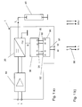
- Fig. 1a shows an inventively designed electronic ballast 1 in a schematic diagram.
- a mains-powered rectifier 10 which the mains voltage in a rectified DC link voltage converts and outputs to an inverter 20.
- the inverter 20 may be formed, for example, as a half-bridge with two switches connected in series between a positive supply voltage and ground, which are controlled via the control device designed as a microcontroller 30 alternately for closing and opening via the control line S.
- the load circuit connected to the inverter 20 has a discharge lamp 40 through which a lamp current i L flows after the ignition process.
- Essential to the present invention is the supply of external brightness control information to the microcontroller 30 via an interface device 50.
- the interface device 50 has an input port 51, which in the described embodiment is designed as a two-wire connection to the connections 51a, 51b. In an embodiment not shown, an input port may be provided with more than two ports.
- the interface device 50 is designed such that brightness control information can be applied to the input port 51 both in the form of control signals which are generated by means of a switch or a pushbutton and in the form of external digital control signals.
- Fig. 1b shows in a schematic diagram symbolizes two examples of the provision of such external control signals that can be applied to the port 51.
- a switch 60 connected to mains voltage N, L, external control signals are generated, i. for the duration of the closing of the switch 60, a sinusoidal mains current is emitted.
- a push-button instead of a switch, a push-button may be used, and the push-button or switch may also switch another voltage such as a constant voltage.
- the external control signal generated in this way is generally used in the electronic ballast according to the invention in those cases in which the electronic ballast is used as an independent light control device.
- the supplied external control signals are interpreted by the microcontroller 30 as brightness control information, for example for switching on or off or for dimming the lamp.
- Fig. 1b Right side, the application of an external digital control signal in the form of a DALI (digitally addressable lighting interface) signal indicated symbolized, via which the microcontroller 30 in such applications receives control information, for example, from a central light control device when the ECG as a single component in a lighting system is integrated.
- DALI signals may include, for example, the information for switching on or dimming the lamp or lamps connected to the ECG.
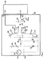
- the interface device 50 of the electronic ballast 10 is embodied such that the control information associated with the external digital control signals is fed to an input port 31 with corresponding input signal terminals 31a, b and the control information associated with the external switching signals is sent to another input port with other input signal terminals 32a, b of the control device 30 be guided.
- the interface device 50 has a first signal path for guiding the control information associated with the external digital control signals from the input port 51 to a first output port 52 having output ports 52a, b and further a second signal path for guiding the control information associated with the external switching signals from the input port 51 to a second output port 53 having output ports 53a, b.
- Each of these output ports 52, 53 is connected to an associated input port or input port 31, 32 of the microcontroller 30. This ensures that at one input port 31, the control information is present for further processing, which corresponds to the external digital control signals and at the other input signal port 32 of the microcontroller 30, the control information is applied, which is associated with the external switching signals, ie corresponding thereto.
- the signal associated with the external DALI signal passes through the phototransistor of the opto-coupler 72 after passing through a signal matching, which by the two resistors 75, 76, the transistor 77 and the diode 78 is realized, on the associated input port 31 of the microcontroller 30.
- the signal waveform described corresponds to the signal path within the interface device 50 on which the control signal is passed, which is the external digital control signal, which is applied to the input port 51 , corresponds.
- the zener diode 80 is designed so that its threshold voltage is greater than the maximum voltage amplitude of the digital signal applied to the input port 51, so that the diode blocks the other signal path for control signals. In the example described, the threshold voltage of the Zener diode is 24V.
- this signal is rectified via the component 70 and can open the second signal path on reaching the threshold voltage at the Zener diode 80, the further via the resistor 81, the photodiode of the optocoupler 82 and the resistor 74 runs.
- the signal associated with the external control signal passes via the phototransistor of the optocoupler 82 to the input port 32 of the microcontroller 30.
- the control information which is assigned to the external control signal and applied to the input port 51 of the interface device 50 is thus fed to the assigned input port 32 of the controller.
- the transistor 79 is turned on, whereby the transistor 71 blocks, so that the first-described signal path is interrupted is. If the external control signal has a sequence of rectangular voltage pulses with an amplitude which is greater than the threshold voltage of the zener diode 80, it is ensured at any time that only one of the two described signal paths to the input port 32 or to the input port 31 is opened.
- Fig. 3 illustrated embodiment of an electronic ballast according to the invention are used, wherein also in FIG. 3 For clarity of illustration only the components microcontroller 30 and the interface device 50 'are shown. Regarding Fig. 2 same components are in Fig. 3 provided with the same reference numerals.
- a normally-off transistor 90 is arranged in the current path which carries the signal associated with the external digital control signal.
- This transistor 90 is switched by a delay element, which is arranged parallel to the input port 51 and the resistor 92, the diode 93 and the integrator capacitor 94 includes, which can transfer the self-locking transistor 90 in the conductive state after a corresponding charge.
- both signal paths of the interface device 50 are initially locked.
- the signal path for the signal which is assigned to a switching signal in turn via the components 70, 80, 81, 82 and 74,79 or from the optocoupler 82 to the associated second Input signal port 32 of the microcontroller 30.
- the latter designates the signal path relevant here to the microcontroller for the brightness control information which is assigned to the external switching signals.
- the input signal received at the port 32 is guided via corresponding components to the reference ground.
- the signal path for the signal passes via the components 70, 90, 72, 73 and 74 or from the phototransistor of the opto-coupler 72 via the level adaptation formed by the components 75-78 to the first input port 31 of FIG Mikrocontrollers 30.
- the latter denotes the signal path relevant here to the microcontroller for the brightness control information, which is assigned to the external digital control signals.
- the signal received at the first input port 31 is internally guided via corresponding components to the reference ground within the controller.
- an external digital control signal for example a DALI signal
- the zener diode 80 blocks the non-normally-off switch 90 because the capacitor C1 initially has no voltage.
- the bridge rectifier 70 outputs an average positive voltage at which the capacitor C1 is charged. After the voltage across the capacitor has been reached in order to drive the transistor 90 for conduction, the signal path for the digital signal is enabled, ie opened, and thus lies against the input port 31 of the microcontroller 30.
- the amount of time necessary to turn on the normally-off transistor 90 depends on the time constant of the RC element and the structure of the digital signal itself. Also at the in Fig. 3 illustrated embodiment is as with reference to Fig. 2 explains, the threshold of the zener diode 80 is set so that it can not be reached when applying an external digital signal at the input port 51, so that the signal path associated with a switching signal is not open.
- the control signals input to the ECG at the input port 51 are switching signals. Will these switching signals as related to Fig. 1b described by switching mains voltage generated, thus is a network pulse train with a frequency of 50 Hz at the input port 51 at.
- This pulse sequence is rectified by means of the bridge 70.
- the capacitor 94 is charged via the resistor 92 and the diode 93.
- the time constant of the delay element is set accordingly.
- the switch 90 It is determined by the resistor 92 and the capacitor 94, and adjusted so that the switch 90 can not go into the conductive state before the threshold voltage of the zener diode 80 is reached and thus the signal path for the external switching signals associated signal is open. Due to the current flow through the resistor 74, the transistor 79 is turned on and thus discharges the capacitor 94, so that the transistor 90 can not go into the conductive state. In the manner described it is ensured that the switch 90 remains locked in any case when the described external switching signal is present at the input port 51. Thus it can be achieved that at no time a signal at the input port 31 of the microcontroller 30 is applied, so that undetermined states can be avoided in the controller.
- an AD converter can also be provided in the signal path which includes the optocoupler 82, so that the input port 32 of the microcontroller 30 in this case is designed to process digital signals.
Landscapes
- Circuit Arrangement For Electric Light Sources In General (AREA)
- Discharge-Lamp Control Circuits And Pulse- Feed Circuits (AREA)
Applications Claiming Priority (1)
| Application Number | Priority Date | Filing Date | Title |
|---|---|---|---|
| DE102010014442A DE102010014442A1 (de) | 2010-04-09 | 2010-04-09 | Elektronisches Vorschaltgerät mit Schnittstellenvorrichtung |
Publications (3)
| Publication Number | Publication Date |
|---|---|
| EP2375868A2 true EP2375868A2 (fr) | 2011-10-12 |
| EP2375868A3 EP2375868A3 (fr) | 2014-12-10 |
| EP2375868B1 EP2375868B1 (fr) | 2016-06-15 |
Family
ID=44343757
Family Applications (1)
| Application Number | Title | Priority Date | Filing Date |
|---|---|---|---|
| EP11159492.5A Active EP2375868B1 (fr) | 2010-04-09 | 2011-03-24 | Appareil de prémontage électronique doté d'un dispositif d'interfaces |
Country Status (4)
| Country | Link |
|---|---|
| EP (1) | EP2375868B1 (fr) |
| AU (1) | AU2011201614B2 (fr) |
| BR (1) | BRPI1101876A2 (fr) |
| DE (1) | DE102010014442A1 (fr) |
Cited By (2)
| Publication number | Priority date | Publication date | Assignee | Title |
|---|---|---|---|---|
| CN109462395A (zh) * | 2018-12-28 | 2019-03-12 | 常州朗奇威电器有限公司 | 接口多路复用转换电路及多路复用转换方法 |
| EP3764746A1 (fr) * | 2019-07-12 | 2021-01-13 | ERCO GmbH | Appareil de commande |
Families Citing this family (1)
| Publication number | Priority date | Publication date | Assignee | Title |
|---|---|---|---|---|
| DE102019125445A1 (de) * | 2019-07-12 | 2021-01-14 | Erco Gmbh | Betriebsgerät |
Citations (1)
| Publication number | Priority date | Publication date | Assignee | Title |
|---|---|---|---|---|
| DE19757295A1 (de) | 1997-03-04 | 1998-09-10 | Tridonic Bauelemente | Elektronisches Vorschaltgerät |
Family Cites Families (5)
| Publication number | Priority date | Publication date | Assignee | Title |
|---|---|---|---|---|
| US5225765A (en) * | 1984-08-15 | 1993-07-06 | Michael Callahan | Inductorless controlled transition and other light dimmers |
| FI95985C (fi) * | 1994-11-24 | 1996-04-10 | Helvar Oy | Menetelmä ja piirijärjestely valaistusteknisen elektroniikkalaitteen ohjaamiseksi |
| US5751118A (en) * | 1995-07-07 | 1998-05-12 | Magnetek | Universal input dimmer interface |
| DE50110394D1 (de) * | 2000-01-14 | 2006-08-17 | Patent Treuhand Ges Fuer Elektrische Gluehlampen Mbh | Vorrichtung und verfahren zur steuerung von betriebsmitteln für mindestens ein elektrisches leuchtmittel |
| DE10319514A1 (de) * | 2003-04-30 | 2004-11-18 | Tridonicatco Gmbh & Co. Kg | Schnittstelle für Digital- und Netzspannungssignale |
-
2010
- 2010-04-09 DE DE102010014442A patent/DE102010014442A1/de not_active Ceased
-
2011
- 2011-03-24 EP EP11159492.5A patent/EP2375868B1/fr active Active
- 2011-04-08 AU AU2011201614A patent/AU2011201614B2/en active Active
- 2011-04-08 BR BRPI1101876-3A patent/BRPI1101876A2/pt not_active IP Right Cessation
Patent Citations (1)
| Publication number | Priority date | Publication date | Assignee | Title |
|---|---|---|---|---|
| DE19757295A1 (de) | 1997-03-04 | 1998-09-10 | Tridonic Bauelemente | Elektronisches Vorschaltgerät |
Cited By (3)
| Publication number | Priority date | Publication date | Assignee | Title |
|---|---|---|---|---|
| CN109462395A (zh) * | 2018-12-28 | 2019-03-12 | 常州朗奇威电器有限公司 | 接口多路复用转换电路及多路复用转换方法 |
| CN109462395B (zh) * | 2018-12-28 | 2023-08-15 | 常州朗奇威电器有限公司 | 接口多路复用转换电路及多路复用转换方法 |
| EP3764746A1 (fr) * | 2019-07-12 | 2021-01-13 | ERCO GmbH | Appareil de commande |
Also Published As
| Publication number | Publication date |
|---|---|
| AU2011201614A1 (en) | 2011-10-27 |
| AU2011201614B2 (en) | 2013-08-29 |
| BRPI1101876A2 (pt) | 2012-10-02 |
| EP2375868B1 (fr) | 2016-06-15 |
| DE102010014442A1 (de) | 2011-10-13 |
| EP2375868A3 (fr) | 2014-12-10 |
Similar Documents
| Publication | Publication Date | Title |
|---|---|---|
| WO2011121011A1 (fr) | Branche émettrice de tension de réseau d'une interface d'un appareil de commande pour moyen d'éclairage | |
| EP2375868B1 (fr) | Appareil de prémontage électronique doté d'un dispositif d'interfaces | |
| EP2154935B1 (fr) | Circuit d'interface pour la transmission de donnée dans un appareil d'eclairage | |
| DE102013219153A1 (de) | Treibermodul mit sekundärseitiger Erkennung einer primärseitigen elektrischen Versorgung | |
| DE3428444C2 (fr) | ||
| EP2638783B1 (fr) | Commande d'un luminaire protégée contre les perturbations | |
| EP1954104B1 (fr) | Interface pour signaux de capteur et signaux numériques dotés d'un circuit protecteur | |
| DE10319514A1 (de) | Schnittstelle für Digital- und Netzspannungssignale | |
| DE10312704A1 (de) | Verfahren zur Ansteuerung und Funktionsüberwachung eines Leistungshalbleiterschalters und Vorrichtung zur Durchführung des Verfahrens | |
| EP1494507B1 (fr) | Interface numérique avec un potentiomètre | |
| DE102007009520B4 (de) | Schnittstelle für Digitalsignale und Netzspannungssignale, mit schaltbarer Konstantstromquelle | |
| EP3895642B1 (fr) | Dispositif de coagulation et/ou de dissection des tissus biologiques et une méthode de fonctionnement d'un dispositif. | |
| AT408392B (de) | Steuereinrichtung für ein elektronisches installationsgerät | |
| EP3123821B1 (fr) | Circuit d'alimentation en tension pour faire fonctionner des led | |
| EP2702838B1 (fr) | Ballast électronique pour un appareil d'éclairage | |
| EP3603345B1 (fr) | Ensemble de circuits et procédé pour faire fonctionner des moyens d'éclairage | |
| AT508809A1 (de) | Schnittstelle für ein betriebsgerät für leuchtmittel | |
| DE102007013758A1 (de) | Schnittstelle mit temperaturkompensiertem Sendezweig | |
| DE102015118725B3 (de) | Betriebsgerät für Gruppenschaltung und Verfahren zum Steuern einer solchen Gruppenschaltung | |
| DE102010028098B4 (de) | Schnittstelle für digitale Niederspannungs- und Netzspannungssignale | |
| DE202012008421U1 (de) | Steuerbares Betriebsgerät | |
| EP0855035B1 (fr) | Procede permettant de faire fonctionner un circuit d'entree et circuit d'entree correspondant | |
| EP2156455A1 (fr) | Dispositif et procédé de détection du mode de commande pour un commutateur à déclenchement de tension ou d'intensité | |
| WO2011038438A1 (fr) | Interface pour un appareil destiné à faire fonctionner des éléments lumineux | |
| AT14758U1 (de) | Treibermodul mit sekundärseitiger Erkennung einer primärseitigen elektrischen Versorgung |
Legal Events
| Date | Code | Title | Description |
|---|---|---|---|
| PUAI | Public reference made under article 153(3) epc to a published international application that has entered the european phase |
Free format text: ORIGINAL CODE: 0009012 |
|
| AK | Designated contracting states |
Kind code of ref document: A2 Designated state(s): AL AT BE BG CH CY CZ DE DK EE ES FI FR GB GR HR HU IE IS IT LI LT LU LV MC MK MT NL NO PL PT RO RS SE SI SK SM TR |
|
| AX | Request for extension of the european patent |
Extension state: BA ME |
|
| PUAL | Search report despatched |
Free format text: ORIGINAL CODE: 0009013 |
|
| AK | Designated contracting states |
Kind code of ref document: A3 Designated state(s): AL AT BE BG CH CY CZ DE DK EE ES FI FR GB GR HR HU IE IS IT LI LT LU LV MC MK MT NL NO PL PT RO RS SE SI SK SM TR |
|
| AX | Request for extension of the european patent |
Extension state: BA ME |
|
| RIC1 | Information provided on ipc code assigned before grant |
Ipc: H05B 37/02 20060101AFI20141104BHEP |
|
| 17P | Request for examination filed |
Effective date: 20150610 |
|
| RBV | Designated contracting states (corrected) |
Designated state(s): AL AT BE BG CH CY CZ DE DK EE ES FI FR GB GR HR HU IE IS IT LI LT LU LV MC MK MT NL NO PL PT RO RS SE SI SK SM TR |
|
| GRAP | Despatch of communication of intention to grant a patent |
Free format text: ORIGINAL CODE: EPIDOSNIGR1 |
|
| INTG | Intention to grant announced |
Effective date: 20160107 |
|
| GRAP | Despatch of communication of intention to grant a patent |
Free format text: ORIGINAL CODE: EPIDOSNIGR1 |
|
| INTG | Intention to grant announced |
Effective date: 20160318 |
|
| GRAS | Grant fee paid |
Free format text: ORIGINAL CODE: EPIDOSNIGR3 |
|
| GRAA | (expected) grant |
Free format text: ORIGINAL CODE: 0009210 |
|
| AK | Designated contracting states |
Kind code of ref document: B1 Designated state(s): AL AT BE BG CH CY CZ DE DK EE ES FI FR GB GR HR HU IE IS IT LI LT LU LV MC MK MT NL NO PL PT RO RS SE SI SK SM TR |
|
| REG | Reference to a national code |
Ref country code: CH Ref legal event code: EP Ref country code: GB Ref legal event code: FG4D Free format text: NOT ENGLISH |
|
| REG | Reference to a national code |
Ref country code: IE Ref legal event code: FG4D Free format text: LANGUAGE OF EP DOCUMENT: GERMAN |
|
| REG | Reference to a national code |
Ref country code: AT Ref legal event code: REF Ref document number: 807079 Country of ref document: AT Kind code of ref document: T Effective date: 20160715 |
|
| REG | Reference to a national code |
Ref country code: DE Ref legal event code: R096 Ref document number: 502011009959 Country of ref document: DE |
|
| REG | Reference to a national code |
Ref country code: LT Ref legal event code: MG4D |
|
| REG | Reference to a national code |
Ref country code: NL Ref legal event code: MP Effective date: 20160615 |
|
| PG25 | Lapsed in a contracting state [announced via postgrant information from national office to epo] |
Ref country code: FI Free format text: LAPSE BECAUSE OF FAILURE TO SUBMIT A TRANSLATION OF THE DESCRIPTION OR TO PAY THE FEE WITHIN THE PRESCRIBED TIME-LIMIT Effective date: 20160615 Ref country code: NO Free format text: LAPSE BECAUSE OF FAILURE TO SUBMIT A TRANSLATION OF THE DESCRIPTION OR TO PAY THE FEE WITHIN THE PRESCRIBED TIME-LIMIT Effective date: 20160915 Ref country code: LT Free format text: LAPSE BECAUSE OF FAILURE TO SUBMIT A TRANSLATION OF THE DESCRIPTION OR TO PAY THE FEE WITHIN THE PRESCRIBED TIME-LIMIT Effective date: 20160615 |
|
| PG25 | Lapsed in a contracting state [announced via postgrant information from national office to epo] |
Ref country code: LV Free format text: LAPSE BECAUSE OF FAILURE TO SUBMIT A TRANSLATION OF THE DESCRIPTION OR TO PAY THE FEE WITHIN THE PRESCRIBED TIME-LIMIT Effective date: 20160615 Ref country code: RS Free format text: LAPSE BECAUSE OF FAILURE TO SUBMIT A TRANSLATION OF THE DESCRIPTION OR TO PAY THE FEE WITHIN THE PRESCRIBED TIME-LIMIT Effective date: 20160615 Ref country code: SE Free format text: LAPSE BECAUSE OF FAILURE TO SUBMIT A TRANSLATION OF THE DESCRIPTION OR TO PAY THE FEE WITHIN THE PRESCRIBED TIME-LIMIT Effective date: 20160615 Ref country code: HR Free format text: LAPSE BECAUSE OF FAILURE TO SUBMIT A TRANSLATION OF THE DESCRIPTION OR TO PAY THE FEE WITHIN THE PRESCRIBED TIME-LIMIT Effective date: 20160615 Ref country code: GR Free format text: LAPSE BECAUSE OF FAILURE TO SUBMIT A TRANSLATION OF THE DESCRIPTION OR TO PAY THE FEE WITHIN THE PRESCRIBED TIME-LIMIT Effective date: 20160916 Ref country code: NL Free format text: LAPSE BECAUSE OF FAILURE TO SUBMIT A TRANSLATION OF THE DESCRIPTION OR TO PAY THE FEE WITHIN THE PRESCRIBED TIME-LIMIT Effective date: 20160615 |
|
| PG25 | Lapsed in a contracting state [announced via postgrant information from national office to epo] |
Ref country code: IT Free format text: LAPSE BECAUSE OF FAILURE TO SUBMIT A TRANSLATION OF THE DESCRIPTION OR TO PAY THE FEE WITHIN THE PRESCRIBED TIME-LIMIT Effective date: 20160615 Ref country code: RO Free format text: LAPSE BECAUSE OF FAILURE TO SUBMIT A TRANSLATION OF THE DESCRIPTION OR TO PAY THE FEE WITHIN THE PRESCRIBED TIME-LIMIT Effective date: 20160615 Ref country code: IS Free format text: LAPSE BECAUSE OF FAILURE TO SUBMIT A TRANSLATION OF THE DESCRIPTION OR TO PAY THE FEE WITHIN THE PRESCRIBED TIME-LIMIT Effective date: 20161015 Ref country code: EE Free format text: LAPSE BECAUSE OF FAILURE TO SUBMIT A TRANSLATION OF THE DESCRIPTION OR TO PAY THE FEE WITHIN THE PRESCRIBED TIME-LIMIT Effective date: 20160615 Ref country code: CZ Free format text: LAPSE BECAUSE OF FAILURE TO SUBMIT A TRANSLATION OF THE DESCRIPTION OR TO PAY THE FEE WITHIN THE PRESCRIBED TIME-LIMIT Effective date: 20160615 Ref country code: SK Free format text: LAPSE BECAUSE OF FAILURE TO SUBMIT A TRANSLATION OF THE DESCRIPTION OR TO PAY THE FEE WITHIN THE PRESCRIBED TIME-LIMIT Effective date: 20160615 |
|
| PG25 | Lapsed in a contracting state [announced via postgrant information from national office to epo] |
Ref country code: PL Free format text: LAPSE BECAUSE OF FAILURE TO SUBMIT A TRANSLATION OF THE DESCRIPTION OR TO PAY THE FEE WITHIN THE PRESCRIBED TIME-LIMIT Effective date: 20160615 Ref country code: SM Free format text: LAPSE BECAUSE OF FAILURE TO SUBMIT A TRANSLATION OF THE DESCRIPTION OR TO PAY THE FEE WITHIN THE PRESCRIBED TIME-LIMIT Effective date: 20160615 Ref country code: ES Free format text: LAPSE BECAUSE OF FAILURE TO SUBMIT A TRANSLATION OF THE DESCRIPTION OR TO PAY THE FEE WITHIN THE PRESCRIBED TIME-LIMIT Effective date: 20160615 Ref country code: PT Free format text: LAPSE BECAUSE OF FAILURE TO SUBMIT A TRANSLATION OF THE DESCRIPTION OR TO PAY THE FEE WITHIN THE PRESCRIBED TIME-LIMIT Effective date: 20161017 |
|
| REG | Reference to a national code |
Ref country code: DE Ref legal event code: R097 Ref document number: 502011009959 Country of ref document: DE |
|
| REG | Reference to a national code |
Ref country code: FR Ref legal event code: PLFP Year of fee payment: 7 |
|
| PLBE | No opposition filed within time limit |
Free format text: ORIGINAL CODE: 0009261 |
|
| STAA | Information on the status of an ep patent application or granted ep patent |
Free format text: STATUS: NO OPPOSITION FILED WITHIN TIME LIMIT |
|
| 26N | No opposition filed |
Effective date: 20170316 |
|
| PG25 | Lapsed in a contracting state [announced via postgrant information from national office to epo] |
Ref country code: DK Free format text: LAPSE BECAUSE OF FAILURE TO SUBMIT A TRANSLATION OF THE DESCRIPTION OR TO PAY THE FEE WITHIN THE PRESCRIBED TIME-LIMIT Effective date: 20160615 |
|
| PG25 | Lapsed in a contracting state [announced via postgrant information from national office to epo] |
Ref country code: SI Free format text: LAPSE BECAUSE OF FAILURE TO SUBMIT A TRANSLATION OF THE DESCRIPTION OR TO PAY THE FEE WITHIN THE PRESCRIBED TIME-LIMIT Effective date: 20160615 |
|
| REG | Reference to a national code |
Ref country code: CH Ref legal event code: PL |
|
| PG25 | Lapsed in a contracting state [announced via postgrant information from national office to epo] |
Ref country code: MC Free format text: LAPSE BECAUSE OF FAILURE TO SUBMIT A TRANSLATION OF THE DESCRIPTION OR TO PAY THE FEE WITHIN THE PRESCRIBED TIME-LIMIT Effective date: 20160615 |
|
| REG | Reference to a national code |
Ref country code: IE Ref legal event code: MM4A |
|
| PG25 | Lapsed in a contracting state [announced via postgrant information from national office to epo] |
Ref country code: LU Free format text: LAPSE BECAUSE OF NON-PAYMENT OF DUE FEES Effective date: 20170324 |
|
| PG25 | Lapsed in a contracting state [announced via postgrant information from national office to epo] |
Ref country code: IE Free format text: LAPSE BECAUSE OF NON-PAYMENT OF DUE FEES Effective date: 20170324 Ref country code: LI Free format text: LAPSE BECAUSE OF NON-PAYMENT OF DUE FEES Effective date: 20170331 Ref country code: CH Free format text: LAPSE BECAUSE OF NON-PAYMENT OF DUE FEES Effective date: 20170331 |
|
| REG | Reference to a national code |
Ref country code: BE Ref legal event code: MM Effective date: 20170331 |
|
| REG | Reference to a national code |
Ref country code: FR Ref legal event code: PLFP Year of fee payment: 8 |
|
| REG | Reference to a national code |
Ref country code: AT Ref legal event code: MM01 Ref document number: 807079 Country of ref document: AT Kind code of ref document: T Effective date: 20170324 |
|
| PG25 | Lapsed in a contracting state [announced via postgrant information from national office to epo] |
Ref country code: BE Free format text: LAPSE BECAUSE OF NON-PAYMENT OF DUE FEES Effective date: 20170331 |
|
| PG25 | Lapsed in a contracting state [announced via postgrant information from national office to epo] |
Ref country code: AT Free format text: LAPSE BECAUSE OF NON-PAYMENT OF DUE FEES Effective date: 20170324 |
|
| PG25 | Lapsed in a contracting state [announced via postgrant information from national office to epo] |
Ref country code: MT Free format text: LAPSE BECAUSE OF FAILURE TO SUBMIT A TRANSLATION OF THE DESCRIPTION OR TO PAY THE FEE WITHIN THE PRESCRIBED TIME-LIMIT Effective date: 20160615 |
|
| PG25 | Lapsed in a contracting state [announced via postgrant information from national office to epo] |
Ref country code: AL Free format text: LAPSE BECAUSE OF FAILURE TO SUBMIT A TRANSLATION OF THE DESCRIPTION OR TO PAY THE FEE WITHIN THE PRESCRIBED TIME-LIMIT Effective date: 20160615 |
|
| PG25 | Lapsed in a contracting state [announced via postgrant information from national office to epo] |
Ref country code: HU Free format text: LAPSE BECAUSE OF FAILURE TO SUBMIT A TRANSLATION OF THE DESCRIPTION OR TO PAY THE FEE WITHIN THE PRESCRIBED TIME-LIMIT; INVALID AB INITIO Effective date: 20110324 |
|
| PG25 | Lapsed in a contracting state [announced via postgrant information from national office to epo] |
Ref country code: BG Free format text: LAPSE BECAUSE OF FAILURE TO SUBMIT A TRANSLATION OF THE DESCRIPTION OR TO PAY THE FEE WITHIN THE PRESCRIBED TIME-LIMIT Effective date: 20160615 |
|
| PG25 | Lapsed in a contracting state [announced via postgrant information from national office to epo] |
Ref country code: CY Free format text: LAPSE BECAUSE OF NON-PAYMENT OF DUE FEES Effective date: 20160615 |
|
| PG25 | Lapsed in a contracting state [announced via postgrant information from national office to epo] |
Ref country code: MK Free format text: LAPSE BECAUSE OF FAILURE TO SUBMIT A TRANSLATION OF THE DESCRIPTION OR TO PAY THE FEE WITHIN THE PRESCRIBED TIME-LIMIT Effective date: 20160615 |
|
| PG25 | Lapsed in a contracting state [announced via postgrant information from national office to epo] |
Ref country code: TR Free format text: LAPSE BECAUSE OF FAILURE TO SUBMIT A TRANSLATION OF THE DESCRIPTION OR TO PAY THE FEE WITHIN THE PRESCRIBED TIME-LIMIT Effective date: 20160615 |
|
| REG | Reference to a national code |
Ref country code: GB Ref legal event code: 732E Free format text: REGISTERED BETWEEN 20230316 AND 20230322 |
|
| REG | Reference to a national code |
Ref country code: DE Ref legal event code: R081 Ref document number: 502011009959 Country of ref document: DE Owner name: OPTOTRONIC GMBH, DE Free format text: FORMER OWNER: BAG ELECTRONICS GMBH, 59759 ARNSBERG, DE Ref country code: DE Ref legal event code: R082 Ref document number: 502011009959 Country of ref document: DE Ref country code: DE Ref legal event code: R081 Ref document number: 502011009959 Country of ref document: DE Owner name: INVENTRONICS GMBH, DE Free format text: FORMER OWNER: BAG ELECTRONICS GMBH, 59759 ARNSBERG, DE |
|
| REG | Reference to a national code |
Ref country code: DE Ref legal event code: R081 Ref document number: 502011009959 Country of ref document: DE Owner name: INVENTRONICS GMBH, DE Free format text: FORMER OWNER: OPTOTRONIC GMBH, 85748 GARCHING, DE |
|
| PGFP | Annual fee paid to national office [announced via postgrant information from national office to epo] |
Ref country code: DE Payment date: 20250319 Year of fee payment: 15 |
|
| PGFP | Annual fee paid to national office [announced via postgrant information from national office to epo] |
Ref country code: FR Payment date: 20250324 Year of fee payment: 15 |
|
| PGFP | Annual fee paid to national office [announced via postgrant information from national office to epo] |
Ref country code: GB Payment date: 20250324 Year of fee payment: 15 |