EP2375496A1 - Absorber für elektromagnetische Strahlung - Google Patents
Absorber für elektromagnetische Strahlung Download PDFInfo
- Publication number
- EP2375496A1 EP2375496A1 EP10003849A EP10003849A EP2375496A1 EP 2375496 A1 EP2375496 A1 EP 2375496A1 EP 10003849 A EP10003849 A EP 10003849A EP 10003849 A EP10003849 A EP 10003849A EP 2375496 A1 EP2375496 A1 EP 2375496A1
- Authority
- EP
- European Patent Office
- Prior art keywords
- substrate
- absorber
- metallic layer
- openings
- recesses
- Prior art date
- Legal status (The legal status is an assumption and is not a legal conclusion. Google has not performed a legal analysis and makes no representation as to the accuracy of the status listed.)
- Withdrawn
Links
Images


Classifications
-
- H—ELECTRICITY
- H01—ELECTRIC ELEMENTS
- H01Q—ANTENNAS, i.e. RADIO AERIALS
- H01Q17/00—Devices for absorbing waves radiated from an antenna; Combinations of such devices with active antenna elements or systems
-
- H—ELECTRICITY
- H01—ELECTRIC ELEMENTS
- H01Q—ANTENNAS, i.e. RADIO AERIALS
- H01Q15/00—Devices for reflection, refraction, diffraction or polarisation of waves radiated from an antenna, e.g. quasi-optical devices
- H01Q15/0006—Devices acting selectively as reflecting surface, as diffracting or as refracting device, e.g. frequency filtering or angular spatial filtering devices
- H01Q15/0013—Devices acting selectively as reflecting surface, as diffracting or as refracting device, e.g. frequency filtering or angular spatial filtering devices said selective devices working as frequency-selective reflecting surfaces, e.g. FSS, dichroic plates, surfaces being partly transmissive and reflective
-
- H—ELECTRICITY
- H05—ELECTRIC TECHNIQUES NOT OTHERWISE PROVIDED FOR
- H05K—PRINTED CIRCUITS; CASINGS OR CONSTRUCTIONAL DETAILS OF ELECTRIC APPARATUS; MANUFACTURE OF ASSEMBLAGES OF ELECTRICAL COMPONENTS
- H05K9/00—Screening of apparatus or components against electric or magnetic fields
- H05K9/0073—Shielding materials
- H05K9/0081—Electromagnetic shielding materials, e.g. EMI, RFI shielding
- H05K9/0088—Electromagnetic shielding materials, e.g. EMI, RFI shielding comprising a plurality of shielding layers; combining different shielding material structure
Definitions
- the invention relates to an absorber for electromagnetic radiation as well as to a method for manufacturing such an absorber.
- Absorbers for electromagnetic radiation are usually layers that cover a device and minimize the reflection of incident electromagnetic waves. They have attracted much interest due to numerous applications in different domains [1]. In tracking applications and the so-called stealth technology, radar absorbers can be used to reduce the radar cross section (RCS) of an object [2]. They are also of interest for shielding electronic circuits and equipments protecting living beings from electromagnetic radiation. In electromagnetic measurement systems, absorbers are indispensable to obtain reliable results. Measurements of electromagnetic compatibility (EMC) and antenna radiation patterns require that spurious signals arising from the test setup and reflections are negligible. This necessitates carrying out the measurements in anechoic chambers.
- EMC electromagnetic compatibility
- antenna radiation patterns require that spurious signals arising from the test setup and reflections are negligible. This necessitates carrying out the measurements in anechoic chambers.
- One of the most effective types of radar absorbers comprises arrays of pyramid shaped pieces made out of a lossy material. [1]-[4].
- An alternative type comprises flat plates of ferrite material in the form of flat tiles fixed to all interior surfaces of the chamber [5].
- Another approach for making absorbers is taking advantage of Salisbury screens which is mainly a resistive sheet in the distance of ⁇ 0 /4 from a ground plane [6]. These kinds of absorbers are usually narrow band devices and they are quite bulky for operating in lower frequencies [7].
- Jaumann absorbers were developed, which are in principle multilayer structures designed to absorb radiation with broader bandwidth [8]. However, these absorbers still suffer from large thickness.
- FSS S frequency selective surfaces
- planar periodic material blocks can also exhibit frequency selective properties
- electromagnetic absorbers based on textured substrates have been proposed.
- an optimization scheme is applied to obtain the best configuration of the textured substrate.
- the resulting substrates are not easily manufacturable. The reason is mainly the need for an intricate texturizing of the substrate in each unit cell.
- the problem to be solved by the present invention is therefore to provide an alternative absorber of this type that has potentially good absorptive properties.
- the absorber of claim 1 comprises a lossy substrate, a first, structured metallic layer arranged on a first side of the substrate and a second metallic layer arranged on a second side of the substrate.
- a plurality of holes in the form of openings or recesses is arranged in the substrate.
- This design has the advantage that the openings or recesses in the substrate affect the resonance properties of the structured metallic layer and the spectral absorption of the whole device. Hence, the presence of the openings or recesses in the substrate allows broadening the spectral response of the absorber.
- Another advantage lies in the fact that a simple structure can be used in the substrate, while the first metallic layer can be structured in more complex manner. Since the substrate is typically perforated or recessed using mechanical methods (such as drilling or punching), a simple structure for the recesses is able to enhance the properties considerably.
- openings extending through the substrate are used. If recesses are used, such recesses advantageously extend from the first side (i.e. the side of the structured metallic layer) into the substrate thus that they have an influence on the resonant properties of the structured first metallic layer.
- manufacturing the recesses requires an accurately controlled process for drilling the substrate and consequently adds to the fabrication cost.
- the absorber further comprises a lossless carrier layer, wherein the first metallic layer is arranged on a surface of this carrier layer.
- a carrier layer mechanically stabilizes the first metallic layer, in particular at the locations of the recesses or openings of the substrate. In addition, it further simplifies the total fabrication process.
- the invention also relates to a method for manufacturing such an absorber.
- Such a method comprises the steps of providing the substrate, mounting the first metallic layer to the substrate, and mounting the second metallic layer to the substrate.
- the absorber comprises a lossless carrier layer, with the first (structured) metallic layer arranged on a surface thereof.
- This design provides mechanical support for the first metallic layer where it extends over the openings or recesses of the substrate.
- the metallic layer is advantageously mounted to a surface of the carrier layer and then the carrier layer and the first metallic layer are mounted to the substrate.
- the carrier layer provides mechanical support for the first metallic layer during the manufacturing process.
- Section 1 the basic geometry of an absorber is described in Section 1.
- Section II a design procedure for such an absorber is described.
- Section III discusses a possible fabrication process and the measurement setup.
- the resulting absorbers are presented in Section IV.
- Some final notes are added in Section V.
- the permittivity and permeability are such that 1 > ⁇ ⁇ ⁇ / ⁇ ⁇ ⁇ > 10 - 2 .
- a “lossless” layer refers to a layer where ⁇ ⁇ ⁇ / ⁇ ⁇ ⁇ ⁇ 10 - 4
- Fig. 1 shows an absorber having a substrate 1 of a lossy material.
- Substrate I is planar and has a width and length much larger than its thickness. Openings or recesses 2 are arranged in substrate 1.
- a structured metallic layer 4 is provided, and on a second side 5 a typically unstructured (i.e. continuous, without any openings) and grounded second metallic layer 6 is mounted.
- Lossy substrate 1 is advantageously of a slightly conducting material having a relative permittivity ⁇ and relative permeability ⁇ in the range defined above. It is e.g. a conducting polymer or a semiconductor. It is typically not a metal because the imaginary parts of the electric permittivity ⁇ of a metal are generally too high.
- openings 2 extending all the way through the substrate I are used.
- recesses as denoted in dotted lines 7 could be used as well.
- the recesses 7 or openings 2 can be empty or they can be filled with a gas or with any other lossless material. However, it is better not to fill with lossy materials since they may reduce the strength of the resonance in the substrate.
- the recesses or openings 2 in substrate 1 are advantageously arranged at regular intervals.
- the recesses or openings 2 have circular cross section, which simplifies the manufacturing process.
- first metallic layer 4 has a lattice structure which is periodic along the two dimensions of the surfaces of substrate 1 with a geometry built up from identical lattice unit cells, with each unit cell covering an identical arrangement of recesses or openings 2.
- a typical periodicity i.e. the unit cell width and height
- c being the speed of light
- ⁇ max a maximum desired absorption frequency of the absorber.
- the size of the unit cells is e.g. 1 cm ⁇ 1 cm.
- each unit cell has mirror symmetry with respect to the directions x and y withe and y being two directions parallel to the surface of absorber 1 and y being perpendicular to x .
- each unit cell has mirror symmetry with respect to the bisectrix of x and y. This results in a substantially isotropic response of the spectral reflectance under 90° rotations of the absorber about an axis perpendicular to its surface.
- the goal of the design of radar absorbers is to obtain very small values of the reflection coefficient. Because of numerical cancelations in the computation of small values, a high accuracy of the analysis method is advantageous. Additionally, the method should be efficient enough to make numerical optimizations possible.
- the periodic method of moments meets the above requirements [15] for the analysis of FSS structures on unperforated substrates. In order to handle the perforations, it is combined with the transmission line method (MoM/TL) [14].
- MoM/TL transmission line method
- MoM basis functions There are two choices for the MoM basis functions, namely rooftop [16] and entire domain basis functions [17]. Because of the existence of several patches (metallic regions) in the unit cell, using entire domain basis functions results in high computation costs. Therefore, rooftop basis functions are the superior choice for our purpose.
- model based parameter estimation MBPE is used to efficiently obtain the reflection spectrum [ 18].
- RHC binary hill climbing
- the RHC algorithm may be described as follows: (1) Perform random initialization and fitness evaluation of the first generation with N pop individuals. (2) Perform bit-fitness value evaluation. (3) Select the best individual (strict elitism) as the parent for the next generation with N (length of the bit string) indivduals. (4) Generate child number n by flipping bit number n of the parent. (5) Repeat step 2 until the parent is better than all of its N children. When this happens, (6) reinitialize the first population using bit fitness proportional (BFP) mutation and continue with step 2 until the stopping criterion is met.
- BFP bit fitness proportional
- a thin, planar absorber which has an optimum bandwidth and angular stability within the intervals 0 GHz ⁇ f ⁇ 30 GHz and 0° ⁇ ⁇ ⁇ 90° is to be obtained.
- similar characteristics for ⁇ and - ⁇ (mirror symmetry) as well as x and y directions (azimuthal symmetry) are desired, with x and y denoting two orthogonal directions parallel to first surface 3 of substrate 1.
- the thickness of the substrate is fixed and needs no optimization. The reasons are the interest in thin radar absorbers, which delimits the thickness to small values, and the commercial availability of substrates with certain thicknesses.
- the periodicity of the substrate is fixed, based on the desired operation frequency.
- the lattice constant for the periodic structure is presumed to be 1 cm.
- a bit string with 28 bits encodes the whole patch unit cell. Since we decided to keep substrate thickness and periodicity constant, there is no variable regarding the substrate that should be optimized, as long as no perforations of the substrate are considered. Thus, the optimization domain is fully defined by a bit string of 28 bits.
- the recesses or openings 2 in substrate 1 need to be optimized as well. For the following, it is assumed that they are in the form of openings extending all the way through substrate 1, even though similar computational methods can be used for modelling recesses as well. Further, it is assumed that the openings are in the form of circular cylindrical holes in order to be easily manufactured. Second, the holes are not manufactured so easily as the patch layer. Therefore, a low number of holes per unit cell area is desirable.
- One way is to analogously subdivide the substrate unit cell by a grid and encode it with a second bit string, in which one indicates the existence of a hole in the pixel center.
- a 6 ⁇ 6 grid is considered in our study (a string of 6 bits) and the hole diameters are fixed to 1 mm ( Fig. 2(b) ).
- Another approach is to assume only one hole per unit cell and optimize its radius and position. Due to the symmetry constraints, the position can be either in the center or on the corners of the unit cell. This is encoded by 1 bit and the radius is chosen by the optimizer among a discrete set of values, namely r ⁇ ⁇ 0.5, 1, 1.5, 2, 2.5, 3, 3.5, 4 ⁇ mm ( Fig. 2(c) ).
- the second approach is the superior choice because-it leads to better results. It should be mentioned that there is room for refinement of the optimization of both types of perforations. In principle, one might combine and generalize these approaches by considering several perforations with diameters and locations to be optimized. This could provide better radar absorbers, but it leads to large bit strings and long computation times and finally to a more demanding manufacturing process.
- the challenging part is to define a compound function that maximizes the above criteria properly.
- a simple possibility is to define a weighted sum of the above function. However, this may incur one function to have a large value and the other one to have a value even below an acceptable limit. For example, the bandwidth which is the most important measure of an absorber may decrease drastically.
- the second term in ⁇ is simply the addition of the normalized functions. The first term gives a large weight to the cases with bandwidths of more than 90% of the maximum bandwidth and a low weight to the ones with narrower bandwidths.
- the optimization process begins with running the optimizer for each of the definitions (1) and (2). This returns ⁇ ⁇ max and f ⁇ max as the result. Subsequently, the optimizer is run again for the compound function. To assist the optimizer to find the optimum faster, one can use the results of the previous runs as initial guesses for the last one.
- first metallic layer 4 can be applied to carrier layer 10 before metallic layer 4 is structured. Then, metallic layer 4 is structured, e.g. by covering it with an etch mask, e.g. using photolithographic or printing techniques. Etching is then used to structure metallic layer 4.
- the recesses or openings 2 in substrate 1 are advantageously formed prior to mounting carrier layer 10 and first metallic layer 4 to substrate 1, thereby simplifying the manufacturing process for substrate 1.
- the optimized absorber is operating based on resonance effects.
- inserting a carrier layer 10 in between the first metallic layer 4 and lossy substrate 1, such as shown in Fig. 3(a) can deteriorate the performance drastically.
- a solution is to paste carrier layer 10 and first metallic layer 4 in upside-down orientation on lossy substrate 1, i.e., in such a way that first metallic layer 4 is arranged between carrier layer 10 and substrate 1, as shown in Fig. 3(b) .
- the thickness of carrier layer 10 is advantageously at least 100 ⁇ m (depending on the operation wavelength) such that it has good mechanical stability for supporting first metallic layer 4 and in addition it is thin enough to have a negligible effect on the whole performance.
- Lossy substrate 1 is the MF-112 absorber material from the ECCOSORB ® MF series with thickness 1.87mm. A measurement was carried out for obtaining the complex relative permittivity ⁇ and relative permeability of the material. The results of this measurement are shown in Fig. 4 .
- Fig. 5 schematically illustrates the measurement setup for characterizing the absorbers.
- the manufactured absorber is placed in front of two horn antennas 11, 12, which are located very close to each other and far from the absorber. Since the experiment is carried out in an anechoic chamber, the two antennas are communicating only through the absorber.
- the transmitted energy between the two antennas is measured once with the absorber and then with a perfect electric conductor (PEC) plane of the same size. Subtracting the obtained two values extracts the reflected energy from the absorber under test.
- PEC perfect electric conductor
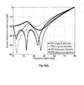
- Fig. 6 the absorption properties of a homogeneous layer with a ground plane on one side is illustrated in Fig. 6 .
- the power reflection coefficient is sketched in terms of the frequency for normal incidence of a plane wave.
- the maximum absorption achieved by this absorber is 12 dB.
- the antenna and its feeding system fail to perform well at low frequencies.
- the measurement results at low frequencies are not reliable.
- there are some sources of errors in the measurement procedure which lead to the observed discrepancies in Fig. 6 . For instance, diffraction from the edges, errors in the measurement of dielectric and magnetic constants using NRW technique, and the small incidence angle in the setup are some of these sources.
- the RHC optimizer is run for the three unit cell configurations shown in Fig. 2 .
- Two different values of R l namely 15 dB and 20 dB, in the fitness functions f ⁇ (BW max ), ⁇ ⁇ (AS max ) and ⁇ are assumed. Since listing the values of ⁇ may not be meaningful, the corresponding values of ⁇ ⁇ and ⁇ 0 that result in the maximum value of ⁇ are presented.
- a better fitness definition - which might result in longer computation times - should result in structures with better angular stability. For instance, if the angular stability would be calculated at the center frequency or averaged over different frequencies, this problem might be solved.
- the fitness definition is highly determined by the particular application for which the absorber is designed.
- the thin lossless carrier layer 10 has a small effect on the absorption properties.
- optimizing without assuming carrier layer 10 seems reasonable.
- a fairly good agreement is observed between the results.
- An important source of error in the measurements is a thin glue layer between first metallic layer 4 and lossy substrate 1.
- the absorbers are resonating structures this small perturbation can incur tangible distortions in the reflection properties.
- Measurement of the oblique incidence needed a larger anechoic chamber than the available one. Hence, measurements are only accomplished for normal incidence.
- Fig. 9(a) there are some gray areas shown in the unit cell of first metallic layer 4. The optimum result indeed included these patches. However, they cause difficulties in the fabrication process since they are placed in close proximity without being electrically connected. In addition, omitting these patches decreases the normalized bandwidth by a negligible value (from 0.5033 to 0.4983). Therefore, the manufactured absorber does not contain the gray patches in Fig. 9(a) .
- a 100% improvement in the bandwidth and 50% enhancement in the relative bandwidth are observed.
- the main reason for the large bandwidth is the appearance of additional resonances when substrate 1 is perforated. This is the main reason for achieving better performance when only one opening 2 in the substrate 1 is presumed. Drilling several smaller openings 2 in substrate 1 pushes the resonances to undesired high frequencies. As a consequence, the absorber can hardly benefit from additional resonances in this case.
- first metallic layer with first metallic structures (denoted in Fig. 9(a) by reference number 14) arranged vertically over one of the recesses or openings 2 and second metallic structures (reference number 15) not arranged over the recesses or openings 2 but rather over the solid bulk of substrate 1.
- the reflected power from the designed absorber at the frequency with maximum absorption remains lower than -15 dB for the incidence angles smaller than 50°.
- this interval calculated at the center frequency is ⁇ ⁇ 52°.
- The.design procedure comprised the following four steps:
Priority Applications (2)
| Application Number | Priority Date | Filing Date | Title |
|---|---|---|---|
| EP10003849A EP2375496A1 (de) | 2010-04-12 | 2010-04-12 | Absorber für elektromagnetische Strahlung |
| PCT/EP2011/001690 WO2011128036A1 (en) | 2010-04-12 | 2011-04-06 | Absorber for electromagnetic radiation |
Applications Claiming Priority (1)
| Application Number | Priority Date | Filing Date | Title |
|---|---|---|---|
| EP10003849A EP2375496A1 (de) | 2010-04-12 | 2010-04-12 | Absorber für elektromagnetische Strahlung |
Publications (1)
| Publication Number | Publication Date |
|---|---|
| EP2375496A1 true EP2375496A1 (de) | 2011-10-12 |
Family
ID=42224192
Family Applications (1)
| Application Number | Title | Priority Date | Filing Date |
|---|---|---|---|
| EP10003849A Withdrawn EP2375496A1 (de) | 2010-04-12 | 2010-04-12 | Absorber für elektromagnetische Strahlung |
Country Status (2)
| Country | Link |
|---|---|
| EP (1) | EP2375496A1 (de) |
| WO (1) | WO2011128036A1 (de) |
Cited By (2)
| Publication number | Priority date | Publication date | Assignee | Title |
|---|---|---|---|---|
| CN103296486A (zh) * | 2012-02-29 | 2013-09-11 | 深圳光启创新技术有限公司 | 一种偏馈微波天线系统 |
| CN107706538A (zh) * | 2016-08-08 | 2018-02-16 | 航天特种材料及工艺技术研究所 | 一种耗散型宽频带吸波fss结构及制备方法 |
Families Citing this family (3)
| Publication number | Priority date | Publication date | Assignee | Title |
|---|---|---|---|---|
| CN108738290B (zh) * | 2018-04-20 | 2019-10-22 | 西北工业大学 | 一种超材料吸波器及设计方法 |
| CN112563759B (zh) * | 2020-11-30 | 2022-06-10 | 合肥工业大学 | 一种双频超宽带超材料吸波单元及吸波体 |
| CN113597246A (zh) * | 2021-07-28 | 2021-11-02 | 维沃移动通信有限公司 | 屏蔽罩和电子设备 |
Citations (2)
| Publication number | Priority date | Publication date | Assignee | Title |
|---|---|---|---|---|
| US2599944A (en) | 1943-05-11 | 1952-06-10 | Us Navy | Absorbent body for electromagnetic waves |
| WO2007080368A1 (en) * | 2006-01-13 | 2007-07-19 | The University Of Sheffield | Absorber |
-
2010
- 2010-04-12 EP EP10003849A patent/EP2375496A1/de not_active Withdrawn
-
2011
- 2011-04-06 WO PCT/EP2011/001690 patent/WO2011128036A1/en active Application Filing
Patent Citations (2)
| Publication number | Priority date | Publication date | Assignee | Title |
|---|---|---|---|---|
| US2599944A (en) | 1943-05-11 | 1952-06-10 | Us Navy | Absorbent body for electromagnetic waves |
| WO2007080368A1 (en) * | 2006-01-13 | 2007-07-19 | The University Of Sheffield | Absorber |
Non-Patent Citations (27)
| Title |
|---|
| "Frequency Selective Surface and Grid Array. New York", 1995, JOHN WILEY AND SONS |
| "Magnetic loading of EBG AMC ground planes and ultrathin absorbers for improved bandwidth performance and reduced size", MICROWAVE AND OPTICAL TECHNOLOGY LETTERS, vol. 48, no. 12, December 2006 (2006-12-01), pages 2468 - 2471 |
| A. FALLAHI; M. MISHRIKEY; C. HAFNER; R. VAHLDIECK: "Analysis of multilayer frequency selective surfaces on periodic and anisotropic substrates", METAMATE- RIALS, vol. 3, no. 2, October 2009 (2009-10-01), pages 63 - 74 |
| A. FALLAHI; M. MISHRIKEY; C. HAFNER; R. VAHLDIECK: "Efficient procedures for the optimization of frequency selective surfaces", ANTENNAS AND PROPAGATION, IEEE TRANSACTIONS ON, vol. 56, no. 5, May 2008 (2008-05-01), pages 1340 - 1349, XP011214339 |
| A. M. NICOLSON; G. F. ROSS: "Measurement of the intrinsic properties of materials by time-domain techniques", INSTRUMENTATION AND MEASUREMENT, IEEE TRANSACTIONS ON, vol. 19, no. 4, 1970, pages 377 - 382, XP001424320 |
| A. N. YUSOFF; M. H. ABDULLAH: "Microwave electromagnetic and absorption properties of some LiZn ferrites", JOURNAL OF MAGNETISM AND MAGNETIC MATERIALS, vol. 269, no. 2, 2004, pages 271 - 280, XP004482353, DOI: doi:10.1016/S0304-8853(03)00617-6 |
| ARYA FALLAHI ET AL: "MoM/RCWA analysis of frequency selective surfaces with inhomogeneous, periodic substrates", ELECTROMAGNETIC COMPATIBILITY, 2007. EMC ZURICH 2007. 18TH INTERNATION AL ZURICH SYMPOSIUM ON, IEEE, PI, 1 September 2007 (2007-09-01), pages 309 - 312, XP031164456, ISBN: 978-3-9523286-1-3 * |
| B. A. MUNK: "Frequency Selective Surfaces Theory and Design.", 2000, JOHN WILEY AND SONS |
| B. DEWITT; W. BURNSIDE: "Electromagnetic scattering by pyramidal and wedge absorber", ANTENNAS AND PROPAGATION, IEEE TRANSACTIONS ON, vol. 36, no. 7, 1988, pages 971 - 984, XP011480694, DOI: doi:10.1109/8.7202 |
| C. CHAN; R. MITTRA: "On the analysis of frequency-selective surfaces using subdomain basis functions", ANTENNAS AND PROPAGATION, IEEE TRANSACTIONS ON, vol. 38, no. I, January 1990 (1990-01-01), pages 40 - 50, XP000135260, DOI: doi:10.1109/8.56991 |
| CHAKRAVARTY S ET AL: "Application of a microgenetic algorithm (MGA) to the design of broadband microwave absorbers using multiple frequency selective surface screens buried in dielectrics", IEEE TRANSACTIONS ON ANTENNAS AND PROPAGATION IEEE USA, vol. 50, no. 3, March 2002 (2002-03-01), pages 284 - 296, XP002601220, ISSN: 0018-926X * |
| CUI S ET AL: "Novel planar electromagnetic absorber designs using genetic algorithms", IEEE TRANSACTIONS ON ANTENNAS AND PROPAGATION IEEE USA, vol. 54, no. 6, June 2006 (2006-06-01), pages 1811 - 1817, XP002601221, ISSN: 0018-926X * |
| D. J. KERN; D. H. WERNER: "A genetic algorithm approach to the design of ultra-thin electromagnetic bandgap absorbers", MICROWAVE AND OPTICAL TECHNOLOGY LETTERS, vol. 38, no. 1, May 2003 (2003-05-01), pages 61 - 64 |
| E. F. KNOTT; J. F. SHAEFFER; M. T. TULEY: "Radar Cross Section.", 1985, ARTECH HOUSE |
| E. MILLER: "Model-based parameter estimation in electromagnetics. i. background and theoretical development", ANTENNAS AND PROPAGATION MAGAZINE. IEEE, vol. 40, no. 1, February 1998 (1998-02-01), pages 42 - 52 |
| FALLAHI A ET AL: "Analysis and optimization of frequency selective surfaces with inhomogeneous periodic substrates", PROCEEDINGS OF THE SPIE - THE INTERNATIONAL SOCIETY FOR OPTICAL ENGINEERING SPIE - THE INTERNATIONAL SOCIETY FOR OPTICAL ENGINEERING USA, vol. 6717, no. 1, 8 October 2007 (2007-10-08), pages 1 - 11, XP002601219, ISSN: 0277-786X * |
| FALLAHI A ET AL: "Analysis of multilayer frequency selective surfaces on periodic and anisotropic substrates", METAMATERIALS OCTOBER 2009 ELSEVIER NLD, vol. 3, no. 2, October 2009 (2009-10-01), pages 63 - 74, XP002601218, DOI: 10.1016/J.METMAT.2009.04.001 * |
| FALLAHI A ET AL: "Radar absorbers based on frequency selective surfaces on perforated substrates", JOURNAL OF COMPUTATIONAL AND THEORETICAL NANOSCIENCE APRIL 2008 AMERICAN SCIENTIFIC PUBLISHERS US, vol. 5, no. 4, April 2008 (2008-04-01), pages 704 - 710, XP009138869, DOI: 10.1166/JCTN.2008.041 * |
| J. WILLIAMS; H. DELGADO; S. LONG: "An antenna pattern measurement technique for eliminating the fields scattered from the edges of a finite ground plane", ANTENNAS AND PROPAGATION, IEEE TRANSACTIONS ON, vol. 38, no. 11, 1990, pages 1815 - 1822, XP000161348, DOI: doi:10.1109/8.102744 |
| L. DU TOIT; J. CLOETE: "Electric screen jauman absorber design algorithms", MICROWAVE THEORY AND TECHNIQUES, IEEE TRANSACTIONS ON, vol. 44, no. 12, 1996, pages 2238 - 2245, XP000636404, DOI: doi:10.1109/22.556452 |
| M. BOZZI; L. PERREGRINI: "Analysis of multilayered printed frequency selective surfaces by the MoM/BI-RME method", ANTENNAS AND PROPAGATION, IEEE TRANSACTIONS ON, vol. 51, no. 10, October 2003 (2003-10-01), pages 2830 - 2836, XP011102040, DOI: doi:10.1109/TAP.2003.817996 |
| N. ENGHETA: "Thin absorbing screens using metamaterial surfaces", PROC. IEEE ANTENNAS AND PROPAGATION SOCIETY INT. SYMP., 2002, pages 392 - 395, XP010591721, DOI: doi:10.1109/APS.2002.1016106 |
| O. BUCCI; G. FRANCESCHETTI: "Scattering from wedge-tapered absorbers", ANTENNAS AND PROPAGATION, IEEE TRANSACTIONS ON, vol. 19, no. 1, 1971, pages 96 - 104 |
| R. FANTE; M. MCCORMACK: "Reflection properties of the salisbury screen", ANTENNAS AND PROPAGATION, IEEE TRANSACTIONS ON, vol. 36, no. 10, 1988, pages 1443 - 1454, XP001382226 |
| S. CUI; D. WEILE; J. VOLAKIS: "Novel planar electromagnetic absorber designs using genetic algorithms", ANTENNAS AND PROPAGATION, IEEE TRANSACTIONS ON, vol. 54, no. 6, 2006, pages 1811 - 1817, XP002601221, DOI: doi:10.1109/TAP.2006.875460 |
| W. H. EMERSON: "Electromagnetic wave absorbers and anechoic chambers through the years", ANTENNAS AND PROPAGATION, IEEE TRANSACTIONS ON, vol. 23, no. 4, 1973, pages 484 - 490, XP001382202 |
| W. WEIR: "Automatic measurement of complex dielectric constant and permeability at microwave frequencies", PROCEEDINGS OF THE IEEE, vol. 62, no. 1, 1974, pages 33 - 36 |
Cited By (4)
| Publication number | Priority date | Publication date | Assignee | Title |
|---|---|---|---|---|
| CN103296486A (zh) * | 2012-02-29 | 2013-09-11 | 深圳光启创新技术有限公司 | 一种偏馈微波天线系统 |
| CN103296486B (zh) * | 2012-02-29 | 2017-07-28 | 深圳光启创新技术有限公司 | 一种偏馈微波天线系统 |
| CN107706538A (zh) * | 2016-08-08 | 2018-02-16 | 航天特种材料及工艺技术研究所 | 一种耗散型宽频带吸波fss结构及制备方法 |
| CN107706538B (zh) * | 2016-08-08 | 2019-11-22 | 航天特种材料及工艺技术研究所 | 一种耗散型宽频带吸波fss结构及制备方法 |
Also Published As
| Publication number | Publication date |
|---|---|
| WO2011128036A1 (en) | 2011-10-20 |
Similar Documents
| Publication | Publication Date | Title |
|---|---|---|
| Fallahi et al. | Thin wideband radar absorbers | |
| Sheokand et al. | An optically transparent broadband microwave absorber using interdigital capacitance | |
| US7256753B2 (en) | Synthesis of metamaterial ferrites for RF applications using electromagnetic bandgap structures | |
| Misran et al. | Design optimisation of ring elements for broadband reflectarray antennas | |
| EP2019447B1 (de) | Elektromagnetischer Bildschirm | |
| Ghosh et al. | Polarisation‐insensitive and wide‐angle multi‐layer metamaterial absorber with variable bandwidths | |
| US20090058746A1 (en) | Evanescent wave-coupled frequency selective surface | |
| Unal et al. | Effective electromagnetic shielding | |
| US20070069940A1 (en) | Method and arrangement for reducing the radar cross section of integrated antennas | |
| Bakir et al. | U‐shaped frequency selective surfaces for single‐and dual‐band applications together with absorber and sensor configurations | |
| Li et al. | Broadband RCS reduction and gain enhancement microstrip antenna using shared aperture artificial composite material based on quasi‐fractal tree | |
| EP2375496A1 (de) | Absorber für elektromagnetische Strahlung | |
| WO2007080368A1 (en) | Absorber | |
| Li et al. | Dual‐polarised and ultra‐thin broadband AAMCs for both P and L bands applications | |
| Kiani‐Kharaji et al. | Wide scan phased array patch antenna with mutual coupling reduction | |
| Inam et al. | Design and characterization of millimeter wave planar reflectarray antenna for 5G communication systems | |
| Varikuntla et al. | Design and development of angularly stable and polarisation rotating FSS radome based on substrate‐integrated waveguide technology | |
| GB2378820A (en) | Electromagnetic filter | |
| Varikuntla et al. | Design of SIW cavity models to control the bandwidth of frequency selective surface | |
| Yu et al. | Miniaturised band‐absorptive frequency selective rasorbers with wide absorption band | |
| Jiang et al. | Design of miniaturised frequency selective rasorber using parallel LC resonators | |
| Sim et al. | Design of electromagnetic wave absorber using periodic structure and method to broaden its bandwidth based on equivalent circuit‐based analysis | |
| Wang et al. | Absorptive/transmissive integrated frequency selective structure based on lumped resistance elements | |
| Hu et al. | Low windage resistance frequency‐selective rasorber based on windmill‐shape coupling line arrays | |
| Jha et al. | Design of a compact microwave absorber using parameter retrieval method for wireless communication applications |
Legal Events
| Date | Code | Title | Description |
|---|---|---|---|
| PUAI | Public reference made under article 153(3) epc to a published international application that has entered the european phase |
Free format text: ORIGINAL CODE: 0009012 |
|
| AK | Designated contracting states |
Kind code of ref document: A1 Designated state(s): AT BE BG CH CY CZ DE DK EE ES FI FR GB GR HR HU IE IS IT LI LT LU LV MC MK MT NL NO PL PT RO SE SI SK SM TR |
|
| AX | Request for extension of the european patent |
Extension state: AL BA ME RS |
|
| STAA | Information on the status of an ep patent application or granted ep patent |
Free format text: STATUS: THE APPLICATION IS DEEMED TO BE WITHDRAWN |
|
| 18D | Application deemed to be withdrawn |
Effective date: 20120413 |